JP5018028B2 - Reference voltage supply circuit, analog circuit and electronic equipment - Google Patents
Reference voltage supply circuit, analog circuit and electronic equipment Download PDFInfo
- Publication number
- JP5018028B2 JP5018028B2 JP2006305154A JP2006305154A JP5018028B2 JP 5018028 B2 JP5018028 B2 JP 5018028B2 JP 2006305154 A JP2006305154 A JP 2006305154A JP 2006305154 A JP2006305154 A JP 2006305154A JP 5018028 B2 JP5018028 B2 JP 5018028B2
- Authority
- JP
- Japan
- Prior art keywords
- circuit
- reference voltage
- operational amplifier
- supply circuit
- frequency
- Prior art date
- Legal status (The legal status is an assumption and is not a legal conclusion. Google has not performed a legal analysis and makes no representation as to the accuracy of the status listed.)
- Expired - Fee Related
Links
Images


Classifications
-
- H—ELECTRICITY
- H04—ELECTRIC COMMUNICATION TECHNIQUE
- H04B—TRANSMISSION
- H04B1/00—Details of transmission systems, not covered by a single one of groups H04B3/00 - H04B13/00; Details of transmission systems not characterised by the medium used for transmission
- H04B1/06—Receivers
- H04B1/16—Circuits
- H04B1/1607—Supply circuits
Landscapes
- Engineering & Computer Science (AREA)
- Computer Networks & Wireless Communication (AREA)
- Signal Processing (AREA)
- Amplifiers (AREA)
- Semiconductor Integrated Circuits (AREA)
- Gyroscopes (AREA)
Description
本発明は、基準電圧供給回路、アナログ回路及び電子機器に関する。 The present invention relates to a reference voltage supply circuit, an analog circuit, and an electronic device.
アナログ回路を構成するトランジスタのノイズには、熱ノイズとフリッカノイズがある。このうち熱ノイズは、高い周波数帯域で支配的なノイズであり、絶対温度に比例する。一方、フリッカノイズは、低い周波数領域で支配的なノイズであり、信号周波数が低くなるにつれてノイズレベルが大きくなる。 The noise of the transistors constituting the analog circuit includes thermal noise and flicker noise. Of these, thermal noise is dominant noise in a high frequency band, and is proportional to absolute temperature. On the other hand, flicker noise is dominant noise in a low frequency region, and the noise level increases as the signal frequency decreases.
一方、電波時計の受信装置やジャイロセンサの検出装置などのアナログ回路では、ミキサ等により周波数の変換が行われる。具体的には、例えばキャリア信号の周波数から所望信号の周波数への変換が行われる。このため、アナログ回路を構成するオペアンプの小振幅増幅の対象となる信号周波数として、高い信号周波数と低い信号周波数が混在する。 On the other hand, in an analog circuit such as a radio clock receiver or a gyro sensor detector, frequency conversion is performed by a mixer or the like. Specifically, for example, conversion from the frequency of the carrier signal to the frequency of the desired signal is performed. For this reason, a high signal frequency and a low signal frequency are mixed as signal frequencies to be subjected to small amplitude amplification of the operational amplifier constituting the analog circuit.
ところが、これまでは、電波時計の受信装置やジャイロセンサの検出装置などのアナログ回路に対してアナログ基準電圧を供給する基準電圧供給回路では、このような信号周波数の違いを考慮したオペアンプの最適なサイジング設計は行われていなかった。また低ノイズと低消費電力の両立に関しても、考慮されていなかった。
本発明は、以上のような技術的課題に鑑みてなされたものであり、その目的とするところは、低ノイズと低消費電力を両立できる基準電圧供給回路、アナログ回路及び電子機器を提供することにある。 The present invention has been made in view of the above technical problems, and an object of the present invention is to provide a reference voltage supply circuit, an analog circuit, and an electronic device that can achieve both low noise and low power consumption. It is in.
本発明は、基準電圧用の第1型のオペアンプを有し、第1のアナログ基準電圧線に対してアナログ基準電圧を供給する第1の供給回路と、基準電圧用の第2型のオペアンプを有し、第2のアナログ基準電圧線に対してアナログ基準電圧を供給する第2の供給回路とを含み、前記基準電圧用の第1型のオペアンプの差動部の差動段トランジスタのチャネル幅をW1aとし、チャネル長をL1aとし、前記基準電圧用の第1型のオペアンプの差動部に流れるバイアス電流をIaとし、前記基準電圧用の第2型のオペアンプの差動部の差動段トランジスタのチャネル幅をW1bとし、チャネル長をL1bとし、前記基準電圧用の第2型のオペアンプの差動部に流れるバイアス電流をIbとした場合に、W1b×L1b>W1a×L1a、Ia>Ibである基準電圧供給回路に関係する。 The present invention includes a first supply circuit for supplying an analog reference voltage to a first analog reference voltage line, and a second type operational amplifier for a reference voltage. And a second supply circuit for supplying an analog reference voltage to a second analog reference voltage line, and a channel width of a differential stage transistor of a differential section of the first-type operational amplifier for the reference voltage Is W1a, the channel length is L1a, the bias current flowing in the differential part of the first-type operational amplifier for the reference voltage is Ia, and the differential stage of the differential part of the second-type operational amplifier for the reference voltage When the channel width of the transistor is W1b, the channel length is L1b, and the bias current flowing through the differential section of the second-type operational amplifier for the reference voltage is Ib, W1b × L1b> W1a × L1a, Ia> Ib so It relates to a reference voltage supply circuit.
本発明によれば、基準電圧供給回路の第1の供給回路は、第1型のオペアンプを用いて、第1のアナログ基準電圧線に対してアナログ基準電圧を供給する。一方、第2の供給回路は、第2型のオペアンプを用いて、第2のアナログ基準電圧線に対して、アナログ基準電圧を供給する。 According to the present invention, the first supply circuit of the reference voltage supply circuit supplies the analog reference voltage to the first analog reference voltage line using the first-type operational amplifier. On the other hand, the second supply circuit supplies an analog reference voltage to the second analog reference voltage line using a second-type operational amplifier.
そして第1型のオペアンプの差動段トランジスタのWL積W1a×L1aと、第2型のオペアンプの差動段トランジスタのWL積W1b×L1bの間には、W1b×L1b>W1a×L1aの関係が成り立つ。従って、第2型のオペアンプのWL積W1b×L1bを大きくできるため、第2型のオペアンプのフリッカノイズを低減できる。これにより、第2の供給回路から供給されるアナログ基準電圧に重畳されるフリッカノイズを最小限に抑えることができる。一方、第1型のオペアンプのWL積W1a×L1aについては小さくできるため、第1型のオペアンプの回路面積が無駄に大きくなる事態を防止できる。 Between the WL product W1a × L1a of the differential stage transistor of the first type operational amplifier and the WL product W1b × L1b of the differential stage transistor of the second type operational amplifier, there is a relationship of W1b × L1b> W1a × L1a. It holds. Therefore, since the WL product W1b × L1b of the second-type operational amplifier can be increased, the flicker noise of the second-type operational amplifier can be reduced. Thereby, the flicker noise superimposed on the analog reference voltage supplied from the second supply circuit can be minimized. On the other hand, since the WL product W1a × L1a of the first-type operational amplifier can be reduced, it is possible to prevent a situation where the circuit area of the first-type operational amplifier becomes unnecessarily large.
また第1型のオペアンプの差動部のバイアス電流Iaと第2型のオペアンプの差動部のバイアス電流Ibの間には、Ia>Ibの関係が成り立つ。従って、第1型オペアンプのバイアス電流Iaを大きくできるため、第1型のオペアンプの熱ノイズを低減できる。従って、第1の供給回路から供給されるアナログ基準電圧に重畳される熱ノイズを最小限に抑えることができる。一方、第2型のオペアンプのバイアス電流Ibについては小さくできるため、第2型のオペアンプの消費電流が無駄に大きくなる事態を防止できる。 Further, a relationship of Ia> Ib is established between the bias current Ia of the differential section of the first-type operational amplifier and the bias current Ib of the differential section of the second-type operational amplifier. Therefore, since the bias current Ia of the first type operational amplifier can be increased, the thermal noise of the first type operational amplifier can be reduced. Therefore, thermal noise superimposed on the analog reference voltage supplied from the first supply circuit can be minimized. On the other hand, since the bias current Ib of the second-type operational amplifier can be reduced, it is possible to prevent the consumption current of the second-type operational amplifier from becoming unnecessarily large.
また本発明では、前記第1の供給回路からアナログ基準電圧が供給される第1の回路における増幅対象信号の周波数をf1とし、前記第2の供給回路からアナログ基準電圧が供給される第2の回路における増幅対象信号の周波数をf2とし、周波数−ノイズ特性におけるフリッカノイズと熱ノイズのコーナ周波数をfcrとした場合に、前記基準電圧用の第1型のオペアンプでは、f1−fcr<fcr−f2であり、前記基準電圧用の第2型のオペアンプでは、fcr−f2<f1−fcrであってもよい。 In the present invention, the frequency of the amplification target signal in the first circuit to which the analog reference voltage is supplied from the first supply circuit is f1, and the second reference circuit is supplied with the analog reference voltage from the second supply circuit. When the frequency of the signal to be amplified in the circuit is f2 and the corner frequency of flicker noise and thermal noise in the frequency-noise characteristic is fcr, in the first-type operational amplifier for the reference voltage, f1−fcr <fcr−f2 In the second-type operational amplifier for the reference voltage, fcr−f2 <f1−fcr may be satisfied.
このようにf1−fcr<fcr−f2の関係が成り立てば、周波数f1側にコーナ周波数fcrを近づけることができ、オペアンプの低ノイズ化と低消費電力化を両立できる。またfcr−f2<f1−fcrの関係が成り立てば、周波数f2側にコーナ周波数fcrを近づけることができ、オペアンプの低ノイズ化と小面積化を両立できる。 Thus, if the relationship of f1−fcr <fcr−f2 is established, the corner frequency fcr can be brought closer to the frequency f1 side, and both noise reduction and power consumption reduction of the operational amplifier can be achieved. If the relationship of fcr−f2 <f1−fcr is established, the corner frequency fcr can be made closer to the frequency f2 side, and both the noise reduction and the area reduction of the operational amplifier can be achieved.
また本発明では、前記基準電圧用の第2型のオペアンプの差動部の能動負荷段トランジスタのチャネル長をL3bとした場合に、L1b<L3bであってもよい。 In the present invention, when the channel length of the active load stage transistor of the differential section of the second-type operational amplifier for the reference voltage is L3b, L1b <L3b may be satisfied.
このようにすれば、第2型のオペアンプでのフリッカノイズを更に低減できる。 In this way, flicker noise in the second-type operational amplifier can be further reduced.
また本発明では、前記基準電圧用の第1型のオペアンプの前記差動段トランジスタのWL比をRT1aとし、前記基準電圧用の第1型のオペアンプの能動負荷段トランジスタのWL比をRT3aとした場合に、RT1a>RT3aであってもよい。 In the present invention, the WL ratio of the differential stage transistor of the first type operational amplifier for the reference voltage is RT1a, and the WL ratio of the active load stage transistor of the first type operational amplifier for the reference voltage is RT3a. In some cases, RT1a> RT3a may be satisfied.
このようにすれば、第1型のオペアンプでの熱ノイズを更に低減できる。 In this way, thermal noise in the first-type operational amplifier can be further reduced.
また本発明では、前記基準電圧用の第2型のオペアンプの前記差動段トランジスタの実効ゲート電圧をVeffとし、ドレイン・ソース間に流れる電流をIdsとし、移動度をμとし、単位面積あたりのゲート容量をCoxとし、WL比をRT1bとし、ボルツマン定数をkとし、絶対温度をTとし、電子電荷量をqとし、プロセス変動パラメータをP(P>1)とした場合に、P×(k×T/q)>Veff={2×Ids/(μ×Cox×RT1b)}1/2>k×T/qの関係を満たす比に、前記WL比RT1bが設定されていてもよい。 In the present invention, the effective gate voltage of the differential stage transistor of the second-type operational amplifier for the reference voltage is Veff, the current flowing between the drain and the source is Ids, the mobility is μ, and the per unit area When the gate capacitance is Cox, the WL ratio is RT1b, the Boltzmann constant is k, the absolute temperature is T, the electronic charge is q, and the process variation parameter is P (P> 1), P × (k × T / q)> Veff = {2 × Ids / (μ × Cox × RT1b)} 1/2 > k × T / q may be set as the WL ratio RT1b.
このようにすれば、第2型のオペアンプの差動段トランジスタが弱反転領域や弱反転領域と強反転領域の境界で動作するのを防止できるため、WL比RT1bを大きくしすぎることによるフリッカノイズの増加を最小限に抑えることができる。 In this way, the differential stage transistor of the second-type operational amplifier can be prevented from operating at the weak inversion region or the boundary between the weak inversion region and the strong inversion region, so flicker noise caused by making the WL ratio RT1b too large. The increase of can be minimized.
また本発明では、前記基準電圧用の第2型のオペアンプを構成する素子のうち前記差動段トランジスタの配置領域の面積をSdfとし、前記基準電圧用の第2型のオペアンプを構成する素子のうち前記差動段トランジスタ以外の素子の配置領域の面積をSreとした場合に、Sdf>Sreであってもよい。 According to the present invention, among the elements constituting the second type operational amplifier for the reference voltage, the area of the arrangement region of the differential stage transistor is Sdf, and the elements constituting the second type operational amplifier for the reference voltage Of these, Sdf> Sre may be satisfied when the area of the arrangement region of elements other than the differential stage transistors is Sre.
このようにすれば、WL積が大きな差動段トランジスタを、Sdfの面積の配置領域に配置することができ、フリッカノイズを低減できる。 In this way, the differential stage transistor having a large WL product can be arranged in the arrangement region having the area of Sdf, and flicker noise can be reduced.
また本発明では、前記基準電圧用の第2型のオペアンプの前記差動段トランジスタは並列接続されたJ個(J>2)のトランジスタにより構成され、前記差動段トランジスタの前記配置領域には、並列接続された前記J個のトランジスタが配置されていてもよい。 In the present invention, the differential stage transistor of the second-type operational amplifier for the reference voltage is composed of J transistors (J> 2) connected in parallel, and the arrangement region of the differential stage transistor is in the arrangement region. The J transistors connected in parallel may be arranged.
このようにすれば、差動段トランジスタのWL積を大きくしながらWL比も大きくできるようになり、フリッカノイズを効率的に低減できる。 In this way, the WL ratio can be increased while increasing the WL product of the differential stage transistor, and flicker noise can be reduced efficiently.
また本発明では、前記基準電圧用の第2型のオペアンプの前記能動負荷段トランジスタは並列接続されたI個(J>I>2)のトランジスタにより構成され、前記差動負荷段トランジスタを構成する前記J個のトランジスタがX方向に沿って並んで配置されると共に、前記J個のトランジスタのY方向側には、前記能動負荷段トランジスタを構成する前記I個のトランジスタがX方向に沿って並んで配置されていてもよい。 In the present invention, the active load stage transistor of the second-type operational amplifier for the reference voltage is composed of I (J> I> 2) transistors connected in parallel to constitute the differential load stage transistor. The J transistors are arranged side by side along the X direction, and the I transistors constituting the active load stage transistor are arranged along the X direction on the Y direction side of the J transistors. May be arranged.
このようにすれば、差動段トランジスタを構成するJ個のトランジスタや能動負荷段トランジスタを構成するI個のトランジスタを、効率良く対称配置できるため、レイアウト効率を向上できる。 In this way, the J transistors constituting the differential stage transistors and the I transistors constituting the active load stage transistors can be efficiently arranged symmetrically, so that the layout efficiency can be improved.
また本発明では、前記第1の供給回路は、前記基準電圧用の第1型のオペアンプを用いて、電圧のインピーダンス変換を行う回路であり、前記第2の供給回路は、前記基準電圧用の第2型のオペアンプを用いて、電圧のインピーダンス変換を行う回路であってもよい。 In the present invention, the first supply circuit is a circuit that performs voltage impedance conversion using a first-type operational amplifier for the reference voltage, and the second supply circuit is for the reference voltage. A circuit that performs voltage impedance conversion using a second-type operational amplifier may be used.
このようにすれば、安定した電位のアナログ基準電圧を供給できるようになる。 In this way, an analog reference voltage having a stable potential can be supplied.
また本発明では、前記第1、第2の供給回路の前段側に設けられ、基準電圧用の第3型のオペアンプを有し、前記第1、第2の供給回路に対して電圧を供給する第3の供給回路を含み、前記基準電圧用の第3型のオペアンプの差動部の差動段トランジスタのチャネル幅をW1cとし、チャネル長をL1cとし、前記基準電圧用の第3型のオペアンプの差動部に流れるバイアス電流をIcとした場合に、W1c×L1c>W1a×L1a、Ic>Ibであってもよい。 In the present invention, a third-type operational amplifier for a reference voltage is provided on the front side of the first and second supply circuits, and supplies a voltage to the first and second supply circuits. A third supply circuit including a third supply circuit, wherein a channel width of the differential stage transistor of the differential section of the third-type operational amplifier for the reference voltage is W1c, a channel length is L1c, and the third-type operational amplifier for the reference voltage W1c × L1c> W1a × L1a and Ic> Ib may be satisfied when the bias current flowing through the differential portion is Ic.
このようにすれば、第3の供給回路の出力電圧の熱ノイズやフリッカノイズを最小限に抑えることができる。従って、出力電圧の熱ノイズが第1の供給回路を介して第1のアナログ基準電圧線に伝達したり、出力電圧のフリッカノイズが第2の供給回路を介して第2のアナログ基準電圧線に伝達する事態を、最小限に抑えることが可能になる。 In this way, thermal noise and flicker noise in the output voltage of the third supply circuit can be minimized. Therefore, thermal noise of the output voltage is transmitted to the first analog reference voltage line via the first supply circuit, or flicker noise of the output voltage is transmitted to the second analog reference voltage line via the second supply circuit. It is possible to minimize the situation of transmission.
また本発明では、W1c×L1c>W1b×L1b、Ic>Iaであってもよい。 In the present invention, W1c × L1c> W1b × L1b and Ic> Ia may be satisfied.
また本発明は、上記のいずれかに記載の基準電圧供給回路と、前記基準電圧供給回路の前記第1の供給回路から、前記第1のアナログ基準電圧線を介してアナログ基準電圧が供給される第1の回路と、前記基準電圧供給回路の前記第2の供給回路から、前記第2のアナログ基準電圧線を介してアナログ基準電圧が供給される第2の回路とを含むアナログ回路に関係する。 According to the present invention, an analog reference voltage is supplied from the reference voltage supply circuit according to any one of the above and the first supply circuit of the reference voltage supply circuit via the first analog reference voltage line. The present invention relates to an analog circuit including a first circuit and a second circuit to which an analog reference voltage is supplied from the second supply circuit of the reference voltage supply circuit via the second analog reference voltage line. .
本発明によれば、第1の供給回路から第1の回路に対して供給されるアナログ基準電圧の熱ノイズを低減できると共に、第2の供給回路から第2の回路に対して供給されるアナログ基準電圧のフリッカノイズを低減できる。従って、第1、第2の回路の熱ノイズ、フリッカノイズを低減でき、アナログ回路のSNR(Signal-to-Nose Ratio)を向上できる。 According to the present invention, the thermal noise of the analog reference voltage supplied from the first supply circuit to the first circuit can be reduced, and the analog supplied from the second supply circuit to the second circuit. Reference voltage flicker noise can be reduced. Therefore, the thermal noise and flicker noise of the first and second circuits can be reduced, and the SNR (Signal-to-Nose Ratio) of the analog circuit can be improved.
また本発明では、所望信号を含む信号に対して所与の周波数の信号をミキシングするミキサを含み、前記第1の回路は、前記ミキサの前段側に設けられる回路であり、前記第2の回路は、前記ミキサの後段側に設けられる回路であってもよい。 The present invention further includes a mixer that mixes a signal having a given frequency with a signal including a desired signal, wherein the first circuit is a circuit provided on the front side of the mixer, and the second circuit May be a circuit provided on the subsequent stage side of the mixer.
このようなミキサを設けると、ミキサの前段側の第1の回路での信号周波数とミキサの後段側の第2の回路での信号周波数が異なるようになる。この場合にも本発明によれば、第1、第2の回路にアナログ基準電圧を供給する基準電圧供給回路において、第1型のオペアンプと第2型のオペアンプを使い分けることで、低ノイズ化と低消費電力化を両立できる。 When such a mixer is provided, the signal frequency in the first circuit on the front stage side of the mixer is different from the signal frequency in the second circuit on the rear stage side of the mixer. Also in this case, according to the present invention, in the reference voltage supply circuit for supplying the analog reference voltage to the first and second circuits, the first-type operational amplifier and the second-type operational amplifier are selectively used to reduce noise. Both low power consumption can be achieved.
また本発明では、前記第1の回路は、入力信号を増幅する第1の増幅回路であり、前記基準電圧供給回路は、前記第1の増幅回路に対して前記第1のアナログ基準電圧線を介してアナログ基準電圧を供給するようにしてもよい。 In the present invention, the first circuit is a first amplifier circuit that amplifies an input signal, and the reference voltage supply circuit connects the first analog reference voltage line to the first amplifier circuit. An analog reference voltage may be supplied through the interface.
このようにすれば、第1の増幅回路での熱ノイズを低減でき、アナログ回路のノイズを低減できる。 In this way, thermal noise in the first amplifier circuit can be reduced, and noise in the analog circuit can be reduced.
また本発明では、前記第2の回路は、前記ミキサからのミキシング後の信号を増幅する第2の増幅回路又はミキシング後の信号のフィルタ処理を行うフィルタ部であり、前記基準電圧供給回路は、前記第2の増幅回路又は前記フィルタ部に対して前記第2のアナログ基準電圧線を介してアナログ基準電圧を供給するようにしてもよい。 Further, in the present invention, the second circuit is a second amplifier circuit that amplifies the signal after mixing from the mixer or a filter unit that performs filtering processing of the signal after mixing, and the reference voltage supply circuit includes: An analog reference voltage may be supplied to the second amplifier circuit or the filter unit via the second analog reference voltage line.
このようにすれば、第2の増幅回路又はフィルタ部でのフリッカノイズを低減でき、アナログ回路のノイズを低減できる。 In this way, flicker noise in the second amplifier circuit or filter unit can be reduced, and noise in the analog circuit can be reduced.
また本発明は、上記のいずれかに記載のアナログ回路と、前記検出装置の検出情報に基づいて処理を行う処理部とを含む電子機器に関係する。 The present invention also relates to an electronic device including any one of the analog circuits described above and a processing unit that performs processing based on detection information of the detection device.
以下、本発明の好適な実施の形態について詳細に説明する。なお以下に説明する本実施形態は特許請求の範囲に記載された本発明の内容を不当に限定するものではなく、本実施形態で説明される構成の全てが本発明の解決手段として必須であるとは限らない。例えば以下では、本発明が適用される基準電圧供給回路として、電波時計の受信装置やジャイロセンサの検出装置のアナログ回路にアナログ基準電圧を供給する回路を例にとり説明するが、本発明はこれに限定されない。 Hereinafter, preferred embodiments of the present invention will be described in detail. The present embodiment described below does not unduly limit the contents of the present invention described in the claims, and all the configurations described in the present embodiment are indispensable as means for solving the present invention. Not necessarily. For example, in the following, a reference voltage supply circuit to which the present invention is applied will be described by taking, as an example, a circuit that supplies an analog reference voltage to an analog circuit of a radio clock receiver or a gyro sensor detector. It is not limited.
1.基準電圧供給回路、アナログ回路の構成
図1に本実施形態の基準電圧供給回路20や、この基準電圧供給回路20を含むアナログ回路(アナログフロントエンド回路)300の構成例を示す。アナログ回路300は、第1の回路310と第2の回路320を含む。
1. Configuration of Reference Voltage Supply Circuit and Analog Circuit FIG. 1 shows a configuration example of the reference
ここで第1の回路310は、増幅対象信号(オペアンプの小信号増幅の対象となる信号)の周波数が第1の周波数となる回路である。また第2の回路320は、増幅対象信号の周波数が第1の周波数よりも低い第2の周波数となる回路である。
Here, the
例えば第1の回路310には、アンテナ、センサ等からの第1の周波数の入力信号(受信信号、センサ信号)が入力される。第1の回路310は、例えば増幅回路を含み、この増幅回路が入力信号の増幅を行う。この場合、増幅対象信号である入力信号(キャリア信号)は、高い第1の周波数の信号となる。
For example, a first frequency input signal (received signal, sensor signal) from an antenna, a sensor, or the like is input to the
第1の回路310と第2の回路320の間には、ミキサ(周波数変換回路)322を設けることができる。即ち第1の回路310は、ミキサ322の前段側に設けられる回路とすることができ、第2の回路320は、ミキサ322の後段側に設けられる回路とすることができる。そしてミキサ322は、所望信号を含む信号に対して所与の周波数の信号(例えば局周波数信号、同期信号)をミキシングする。
A mixer (frequency conversion circuit) 322 can be provided between the
第2の回路320には、ミキサ322によるミキシング(周波数変換)により第2の周波数に変換された信号が入力される。第2の回路320の増幅回路、フィルタ部又は出力回路は、増幅対象信号である第2の周波数の信号についての小振幅増幅を行う。
The signal converted to the second frequency by mixing (frequency conversion) by the
基準電圧供給回路20は、第1の回路310や第2の回路320に対してAGND(広義にはアナログ基準電圧)を供給する。この基準電圧供給回路20は第1の供給回路21と第2の供給回路22を含む。第1の供給回路21は、第1の回路310に対してAGND(アナロググランド)を供給する。第2の供給回路22は、第2の回路320に対してAGNDを供給する。また第1の供給回路21は、基準電圧用の第1型のオペアンプOP1を有し、第2の供給回路22は、基準電圧用の第2型のオペアンプOP2を有する。
The reference
ここで基準電圧用の第1型のオペアンプOP1は、例えば第2型のオペアンプOP2に比べて第1の周波数(例えばキャリア周波数、変調周波数、共振周波数)での熱ノイズが低いオペアンプとなっている。一方、基準電圧用の第2型のオペアンプOP2は、第1型のオペアンプOP1に比べて第2の周波数(例えばキャリア信号により搬送される所望信号の周波数、所望信号の周波数帯域の最大周波数)でのフリッカノイズが低いオペアンプとなっている。 Here, the first-type operational amplifier OP1 for the reference voltage is an operational amplifier with lower thermal noise at the first frequency (for example, carrier frequency, modulation frequency, resonance frequency) than the second-type operational amplifier OP2, for example. . On the other hand, the second-type operational amplifier OP2 for the reference voltage has a second frequency (for example, the frequency of the desired signal carried by the carrier signal, the maximum frequency in the frequency band of the desired signal) as compared with the first-type operational amplifier OP1. The operational amplifier has low flicker noise.
具体的には、第1の回路310における増幅対象信号(第1の回路310が含むオペアンプの増幅対象信号)の周波数(例えば数十KHz〜数百KHz)をf1とし、第2の回路320における増幅対象信号(第1の回路320が含むオペアンプの増幅対象信号)の周波数(例えば数Hz〜数百Hz)をf2とし、フリッカノイズと熱ノイズのコーナ周波数をfcrとしたとする。この場合に、第1型のオペアンプOP1では、例えばf1−fcr<fcr−f2の関係が成り立つようになっている。即ちコーナ周波数fcrの近傍の周波数にf1が設定されるように、第1型のオペアンプOP1のサイジングが行われる。また第2型のオペアンプOP2では、例えばfcr−f2<f1−fcrの関係が成り立つようになっている。即ちコーナ周波数fcrの近傍の周波数にf2が設定されるように、第2型のオペアンプOP2のサイジングが行われる。
Specifically, the frequency (for example, several tens KHz to several hundred KHz) of the signal to be amplified in the first circuit 310 (the signal to be amplified by the operational amplifier included in the first circuit 310) is f1, and the
また、第1型のオペアンプOP1の差動部の差動段トランジスタのチャネル幅をW1aとし、チャネル長をL1aとし、差動部に流れるバイアス電流(電流値)をIaとしたとする。また第2型のオペアンプOP2の差動部の差動段トランジスタのチャネル幅をW1bとし、チャネル長をL1bとし、差動部に流れるバイアス電流をIbとしたとする。この場合に、例えばW1b×L1b>W1a×L1a、Ia>Ibの関係が成り立つようになっている。 Further, the channel width of the differential stage transistor in the differential section of the first-type operational amplifier OP1 is W1a, the channel length is L1a, and the bias current (current value) flowing through the differential section is Ia. Further, it is assumed that the channel width of the differential stage transistor in the differential section of the second-type operational amplifier OP2 is W1b, the channel length is L1b, and the bias current flowing in the differential section is Ib. In this case, for example, the relationship of W1b × L1b> W1a × L1a and Ia> Ib is established.
また図1に示すように基準電圧供給回路20は第3の供給回路23を含むことができる。この第3の供給回路23は、第1、第2の供給回路21、22の前段側に設けられ、第1、第2の供給回路21、22に対して出力電圧V3Qを供給する。第1、第2の供給回路21、22は、第3の供給回路23からの出力電圧V3Qのインピーダンス変換を行って、AGNDを出力する。
As shown in FIG. 1, the reference
そして第3の供給回路23は、基準電圧用の第3型のオペアンプOP3を含む。この基準電圧用の第3型のオペアンプOP3は、第2型のオペアンプOP2(或いはOP1)に比べてキャリア信号の周波数での熱ノイズが低く、第1型のオペアンプOP1(或いはOP2)に比べて所望信号の周波数でのフリッカノイズが低いオペアンプとなっている。例えば第3型のオペアンプOP3の差動部の差動段トランジスタのチャネル幅をW1cとし、チャネル長をL1cとし、差動部に流れるバイアス電流をIcとした場合に、W1c×L1c>W1a×L1a、Ic>Ibの関係が成り立つ。或いはW1c×L1c>W1b×L1b、Ic>Iaの関係が成り立ってもよい。
The
図2、図3にアナログ回路300の例として電波時計の受信装置の構成例を示す。なお受信装置は図2、図3の構成に限定されず、その構成要素の一部を省略したり、他の構成要素を追加するなどの種々の変形実施が可能である。
2 and 3 show configuration examples of a radio clock receiver as an example of the
図2の受信装置はダイレクトコンバージョン方式の例である。現在、各国(日本、ドイツ、イギリス等)において、時刻データであるタイムコード入りの長波標準電波が送出されている。日本では、2つの送信所から、タイムコードで振幅変調された40KHz及び60KHzの長波標準電波が送出されている。即ち60秒を1サイクルとして時刻データがバイナリデータとして送出される。電波時計は、このようなタイムコードの電波を受信し、計時回路の時刻データを修正する。このため電波時計の受信装置は、受信した電波を検波及び復調することで、所望の周波数の信号を抽出して、タイムコードを取得する。 The receiving apparatus in FIG. 2 is an example of a direct conversion method. Currently, in each country (Japan, Germany, UK, etc.), a long wave standard radio wave including a time code as time data is transmitted. In Japan, 40 KHz and 60 KHz long-wave standard radio waves modulated with time codes are transmitted from two transmitting stations. That is, time data is transmitted as binary data with 60 seconds as one cycle. The radio timepiece receives the radio wave of such a time code and corrects the time data of the clock circuit. For this reason, the receiving device of the radio timepiece extracts a signal of a desired frequency by detecting and demodulating the received radio wave, and acquires a time code.
具体的には図2において、バーアンテナ等で構成されるアンテナ330が長波標準電波を受信し、受信された電波は電気信号に変換されて出力される。増幅回路(RF増幅回路)332は、アンテナ330からの信号を増幅して出力する。フィルタ部334は、例えばハイパスフィルタの周波数特性を有し、増幅回路332からの信号のフィルタ処理を行う。
Specifically, in FIG. 2, an
ミキサ(周波数変換回路)336は、フィルタ部334からの信号に対して、局部発振回路344からの局部発振周波数の信号をミキシングすることで、直接にベースバンド信号(数Hz)に変換するダイレクトコンバージョンを行う。
The mixer (frequency conversion circuit) 336 directly converts the signal from the
増幅回路338は、ミキサ336からの信号を増幅する。フィルタ部340は、例えばローパスフィルタの周波数特性を有し、増幅回路338からの信号のフィルタ処理を行う。復調部342は、フィルタ部340からの信号の復調を行い、復調により得られたタイムコードを出力する。電波時計では、このタイムコードにより時刻データの修正が行われる。
The
図3の受信装置はスーパーヘテロダイン方式の例である。増幅回路352はアンテナ350からの信号を増幅する。フィルタ部354は、例えばバンドパスフィルタの周波数特性を有し、増幅回路352からの信号のフィルタ処理を行う。
The receiving apparatus in FIG. 3 is an example of a superheterodyne system. The
ミキサ356は、フィルタ部354からの信号に対して、局部発振回路364からの局部発振周波数の信号をミキシングすることで、中間周波数(数百Hz)の信号を生成するスーパーヘテロダイン方式の変換を行う。
The
フィルタ部358は、例えばバンドパスフィルタの周波数特性を有し、ミキサ356からの信号に対して中間周波数を中心とした所定範囲の周波数成分を通過させて、範囲外の周波数成分を遮断する。検波回路360は、フィルタ部358からの信号の検波(例えば包絡線検波)を行う。復調部362は、検波回路360からの検波信号の復調を行い、復調により得られたタイムコードを出力する。
The
そして図2では、例えば増幅回路332(第1の増幅回路)やフィルタ部334が図1の第1の回路310になり、第1の供給回路21は、この増幅回路332やフィルタ部334に対してAGND線(アナログ基準電圧線)AGL1を介してAGND(アナログ基準電圧)を供給することができる。
In FIG. 2, for example, the amplifier circuit 332 (first amplifier circuit) and the
また図2では、例えば増幅回路338(第2の増幅回路)やフィルタ部340が図1の第2の回路320になり、第2の供給回路22は、この増幅回路338やフィルタ部340に対してAGND線AGL2を介してAGNDを供給することができる。
In FIG. 2, for example, the amplifier circuit 338 (second amplifier circuit) and the
また図3では、例えば増幅回路352やフィルタ部354が図1の第1の回路310になり、第1の供給回路21は、この増幅回路352やフィルタ部354に対してAGND線AGL1を介してAGNDを供給することができる。
In FIG. 3, for example, the
また図3では、例えばフィルタ部358や検波回路360が図1の第2の回路320になり、第2の供給回路22は、このフィルタ部358や検波回路360に対してAGND線AGL2を介してAGNDを供給することができる。
In FIG. 3, for example, the
なお本実施形態の基準電圧供給回路20によりAGND(アナログ基準電圧)が供給されるアナログ回路300は、図2、図3のような電波時計の受信装置に限定されない。例えば赤外線リモコンにおける受信装置に適用したり、後述するジャイロセンサなどの各種センサの検出装置に適用してもよい。
The
また図1の第1の回路310は前述した第1型のオペアンプOP1を含むことができ、第2の回路320は前述した第2型のオペアンプOP2を含むことができる。同様に図2の増幅回路332、フィルタ部334や、図3の増幅回路352、フィルタ部354は、第1型のオペアンプOP1を含むことができる。また図2の増幅回路338、フィルタ部340や、図3のフィルタ部358、検波回路360は、第2型のオペアンプOP2を含むことできる。これにより、これらの回路での熱ノイズやフリッカノイズを低減でき、SNRを更に向上できる。
1 may include the first-type operational amplifier OP1 described above, and the
2.低ノイズ化手法
2.1 ノイズ解析
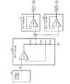
図4(A)に本実施形態で使用されるオペアンプの構成例を示す。このオペアンプは差動部200と出力部210を含む。
2. 2. Noise Reduction Technique 2.1 Noise Analysis FIG. 4A shows a configuration example of an operational amplifier used in this embodiment. This operational amplifier includes a
差動部200は、差動段トランジスタM1、M2と能動負荷段トランジスタM3、M4を含む。またバイアス段トランジスタM5を含む。差動段トランジスタM1、M2は、ノードN1とノードN2、N3との間に設けられ、そのゲートに差動の入力信号IM、IPが入力される。能動負荷段M3、M4は、ノードN2、N3と第1の電源との間に設けられ、そのゲートにノードN2が接続される。バイアス段トランジスタM5は、VDD(第2の電源)とノードN1との間に設けられる。このバイアス段トランジスタM5のゲートには、トランジスタM8及び電流源ISにより構成されるバイアス回路212のバイアスノードN4が接続される。これにより、バイアス回路212のバイアス電流IBSに応じたバイアス電流IBDが差動部200に流れる。
The
出力部210は、第2の電源(VDD)と第1の電源の間に設けられる駆動段トランジスタM6とバイアス段トランジスタM7を含む。駆動段トランジスタM6のゲートには差動部200の出力ノードN3が接続され、バイアス段トランジスタM7のゲートにはバイアスノードN4が接続される。またノードN3、N5間には位相補償用キャパシタCFや抵抗RFが設けられる。
The
なお本実施形態のオペアンプの構成は図4(A)に限定されない。例えば図4(A)では差動段トランジスタM1、M2やバイアス段トランジスタM5がP型トランジスタであり、能動負荷段トランジスタM3、M4がN型トランジスタである場合の例を示しているが、M1、M2、M5がN型トランジスタとなり、M3、M4がP型トランジスタとなる構成であってもよい。また図4(A)の素子(トランジスタ、キャパシタ)の一部を省略したり、他の素子を追加するなどの変形実施も可能である。 Note that the configuration of the operational amplifier according to this embodiment is not limited to that shown in FIG. For example, FIG. 4A shows an example in which the differential stage transistors M1 and M2 and the bias stage transistor M5 are P-type transistors and the active load stage transistors M3 and M4 are N-type transistors. M2 and M5 may be N-type transistors, and M3 and M4 may be P-type transistors. Also, modifications such as omitting a part of the elements (transistors and capacitors) in FIG. 4A and adding other elements are possible.
次に図4(A)のオペアンプのノイズ解析について説明する。図4(B)にトランジスタ単体の小信号振幅の等価回路を示す。ノイズはV2の単位(V2/Hz)で扱われるため、図4(B)の等価回路もV2の単位で扱うことにする。図4(B)の等価回路では、トランジスタの入力換算ノイズ(ゲート換算ノイズ)を計算するために、トランジスタのゲートにノイズSvg=Vn2の電圧源が設けられている。またドレイン・ソース間には、gm2(Vgs2+Vn2)の電流源や1/gds2の抵抗が設けられている。 Next, noise analysis of the operational amplifier in FIG. FIG. 4B shows an equivalent circuit of a small signal amplitude of a single transistor. Noise because it is handled in units of V 2 (V 2 / Hz), it will be handled in units of equivalent circuits V 2 in FIG. 4 (B). In the equivalent circuit of FIG. 4B, in order to calculate the input conversion noise (gate conversion noise) of the transistor, a voltage source of noise Svg = Vn 2 is provided at the gate of the transistor. Between the drain and the source, a current source of gm 2 (Vgs 2 + Vn 2 ) and a resistance of 1 / gds 2 are provided.
図5(A)に示すようにノイズにはフリッカノイズ(1/fノイズ)と熱ノイズがある。フリッカノイズは、ゲート酸化膜とシリコン基板の界面にあるダングリングボンドに電子が捕獲・放出されることで生じるノイズであり、周波数が低くなるほど大きくなる。一方、熱ノイズは、トランジスタのチャネル領域を抵抗と見なした場合に、電子のランダムな動きにより生じるノイズであり、絶対温度に比例する。 As shown in FIG. 5A, noise includes flicker noise (1 / f noise) and thermal noise. Flicker noise is noise that occurs when electrons are captured and emitted from dangling bonds at the interface between the gate oxide film and the silicon substrate, and increases as the frequency decreases. On the other hand, thermal noise is noise generated by random movement of electrons when the channel region of a transistor is regarded as a resistance, and is proportional to absolute temperature.
図4(B)の入力換算ノイズの等価回路において、フリッカノイズ、熱ノイズは、各々、下式(1)(2)のように求められる。 In the equivalent circuit of the input conversion noise in FIG. 4B, flicker noise and thermal noise are obtained as shown in the following equations (1) and (2), respectively.

上式(1)において、Coxはトランジスタの単位面積あたりのゲート容量、Wはチャネル幅、Lはチャネル長、fは周波数、Kは製造プロセスに依存したフリッカノイズの定数である。また上式(2)において、gmはトランス(相互)コンダクタンス、kはボルツマン定数、Tは絶対温度である。 In the above equation (1), Cox is the gate capacitance per unit area of the transistor, W is the channel width, L is the channel length, f is the frequency, and K is a flicker noise constant depending on the manufacturing process. In the above equation (2), gm is a trans (mutual) conductance, k is a Boltzmann constant, and T is an absolute temperature.
本実施形態では、図4(A)のオペアンプの回路を図4(B)の等価回路で置換して、伝達関数を算出する。その際に、オペアンプの全トランジスタのサイズ(W、L)、ノイズレベル、ドレイン・ソース間電流が同じであると仮定し、数値解析により全体の99パーセントを占める上位の項だけを導き出す。すると、オペアンプのノイズSvg(ノイズスペクトラム)は下式(3)のように求められる。 In this embodiment, the transfer function is calculated by replacing the operational amplifier circuit of FIG. 4A with the equivalent circuit of FIG. At that time, assuming that the size (W, L), noise level, and drain-source current of all the transistors of the operational amplifier are the same, only the upper term that accounts for 99% of the whole is derived by numerical analysis. Then, the noise Svg (noise spectrum) of the operational amplifier is obtained as in the following equation (3).
上式(3)において、Vn1、Vn2、Vn3、Vn4は、図4(A)のトランジスタM1、M2、M3、M4のゲート・ノイズ電圧であり、gm1、gm2、gm3、gm4は、トランジスタM1、M2、M3、M4のトランスコンダクタンスである。 In the above equation (3), Vn1, Vn2, Vn3, and Vn4 are gate noise voltages of the transistors M1, M2, M3, and M4 in FIG. 4A, and gm1, gm2, gm3, and gm4 are the transistors M1, This is the transconductance of M2, M3, and M4.
上式(3)の数値解析の結果から明らかなように、オペアンプのノイズSvgは、図4(A)の差動部200の差動段トランジスタM1、M2と能動負荷段トランジスタM3、M4のノイズにより、全体のほとんどが占められていることが理解される。従って、オペアンプのサイジングの際には、これらのトランジスタM1、M2、M3、M4についてのチャネル幅W、チャネル長Lの適正化を図ればよい。
As is apparent from the numerical analysis result of the above equation (3), the noise Svg of the operational amplifier is the noise of the differential stage transistors M1 and M2 and the active load stage transistors M3 and M4 of the
まず、フリッカノイズについて解析する。フリッカノイズについてのゲート・ノイズ電圧Vn1、Vn2、Vn3、Vn4は、上式(1)より下式(4)(5)(6)(7)のように求められる。 First, flicker noise is analyzed. The gate noise voltages Vn1, Vn2, Vn3, and Vn4 for flicker noise are obtained from the above equation (1) as in the following equations (4), (5), (6), and (7).
上式(4)〜(7)において、W1、L1は差動段トランジスタM1、M2のチャネル幅、チャネル長であり、W3、L3は能動負荷段トランジスタM3、M4のチャネル幅、チャネル長である。ここでM2のチャネル幅W2、チャネル長L2は、M1のW1、L1と同じであり、M4のチャネル幅W4、チャネル長L4は、M3のW3、L3と同じであるとしている。またKp,Knは、P型トランジスタ、N型トランジスタのプロセス依存定数である。 In the above equations (4) to (7), W1 and L1 are the channel width and channel length of the differential stage transistors M1 and M2, and W3 and L3 are the channel width and channel length of the active load stage transistors M3 and M4. . Here, the channel width W2 and channel length L2 of M2 are the same as W1 and L1 of M1, and the channel width W4 and channel length L4 of M4 are the same as W3 and L3 of M3. Kp and Kn are process-dependent constants of the P-type transistor and the N-type transistor.
また差動段トランジスタM1、M2のトランスコンダクタンスgm1(=gm2)、能動負荷段トランジスタM3、M4のトランスコンダクタンスgm3(=gm4)は、下式(8)(9)のように求められる。 Further, the transconductance gm1 (= gm2) of the differential stage transistors M1 and M2 and the transconductance gm3 (= gm4) of the active load stage transistors M3 and M4 are obtained by the following equations (8) and (9).
上式(8)(9)において、μp、μnはP型トランジスタ、N型トランジスタの移動度であり、Idsはトランジスタのドレイン・ソース間電流であり、全てのトランジスタM1〜M4においてIdsは同じであるとしている。 In the above equations (8) and (9), μp and μn are the mobility of the P-type transistor and the N-type transistor, Ids is the drain-source current of the transistor, and Ids is the same in all the transistors M1 to M4. There is.
上式(4)〜(9)を上式(3)に代入することで、オペアンプのフリッカノイズSvgFlcは下式(10)のように求められる。 By substituting the above equations (4) to (9) into the above equation (3), the flicker noise SvgFlc of the operational amplifier is obtained as the following equation (10).
次に、熱ノイズについて解析する。熱ノイズについてのゲート・ノイズ電圧Vn1、Vn2、Vn3、Vn4は、上式(2)より下式(11)(12)(13)(14)のように求められる。 Next, thermal noise is analyzed. The gate noise voltages Vn1, Vn2, Vn3, and Vn4 for thermal noise are obtained from the above equation (2) as in the following equations (11), (12), (13), and (14).
上式(11)〜(14)を上式(3)に代入すると、オペアンプの熱ノイズSvgThmは下式(15)のようになる。 When the above equations (11) to (14) are substituted into the above equation (3), the thermal noise SvgThm of the operational amplifier is represented by the following equation (15).
上式(15)に上式(8)(9)を代入することで、オペアンプの熱ノイズSvgThmは下式(16)のように求められる。 By substituting the above equations (8) and (9) into the above equation (15), the thermal noise SvgThm of the operational amplifier is obtained as the following equation (16).
フリッカノイズSvgFlcに関する上式(10)や熱ノイズSvgThmに関する上式(16)において、自然界で決定される定数や、プロセスのみに依存する定数を排除すると、W1、W3、L1、L3、Idsが、設計上管理できる変数になる。従って上式(10)より、フリッカノイズSvgFlcを低減するためには、下記が成り立つ。
(P1)差動段トランジスタM1、M2のWL積W1×L1(ゲート面積)をできるだけ大きくする。これにより上式(10)の第1項が小さくなり、SvgFlcが小さくなる。
(P2)L1/L3の比率をなるべく小さくする。即ち例えばL1<L3とする。これにより、上式(10)の第2項が小さくなり、SvgFlcが小さくなる。また結果的に、能動負荷段トランジスタM3、M4のWL積W3×L3も大きくなる。
(P3)フリッカノイズSvgFlcはIdsには依存しない。従って、フリッカノイズだけを考慮するならば、Idsを小さくすることで、低消費電力化を図れる。
When constants determined in the natural world and constants that depend only on the process are excluded from the above expression (10) regarding the flicker noise SvgFlc and the above expression (16) regarding the thermal noise SvgThm, W1, W3, L1, L3, and Ids are It becomes a variable that can be managed by design. Therefore, from the above equation (10), in order to reduce the flicker noise SvgFlc, the following holds.
(P1) The WL product W1 × L1 (gate area) of the differential stage transistors M1 and M2 is increased as much as possible. As a result, the first term of the above equation (10) becomes small, and SvgFlc becomes small.
(P2) The ratio of L1 / L3 is made as small as possible. That is, for example, L1 <L3. As a result, the second term of the above equation (10) is reduced, and SvgFlc is reduced. As a result, the WL product W3 × L3 of the active load stage transistors M3 and M4 also increases.
(P3) Flicker noise SvgFlc does not depend on Ids. Therefore, if only flicker noise is taken into account, the power consumption can be reduced by reducing Ids.
以上より、フリッカノイズSvgFlcの低減と低消費電力化を両立するためには、差動段トランジスタのWL積W1×L1を大きくすると共に、差動部に流れるバイアス電流IBD(Ids)を小さくすればよいことがわかる。 From the above, in order to achieve both reduction of flicker noise SvgFlc and low power consumption, it is necessary to increase the WL product W1 × L1 of the differential stage transistor and reduce the bias current IBD (Ids) flowing in the differential section. I know it ’s good.
また上式(16)より、熱ノイズSvgThmを低減するためには、下記が成り立つ。
(Q1)電流Ids(IBD)をできるだけ大きくする。これにより上式(16)の第1項及び第2項が小さくなり、SvgThmが小さくなる。
(Q2)差動段トランジスタM1、M2のWL比RT1=W1/L1をできるだけ大きくし、能動負荷段トランジスタM3、M4のWL比RT3=W3/L3をできるだけ小さくする。即ち例えばRT1>RT3とする。
(Q3)熱ノイズSvgThmはWL積W1×L1やW3×L3には依存しない。従って、熱ノイズだけを考慮するならば、W1×L1やW3×L3を小さくすることで、オペアンプの小面積化を図れる。
Further, from the above equation (16), the following holds in order to reduce the thermal noise SvgThm.
(Q1) Increase the current Ids (IBD) as much as possible. As a result, the first term and the second term of the above equation (16) are reduced, and SvgThm is reduced.
(Q2) The WL ratio RT1 = W1 / L1 of the differential stage transistors M1 and M2 is made as large as possible, and the WL ratio RT3 = W3 / L3 of the active load stage transistors M3 and M4 is made as small as possible. That is, for example, RT1> RT3.
(Q3) The thermal noise SvgThm does not depend on the WL product W1 × L1 or W3 × L3. Therefore, if only thermal noise is considered, the area of the operational amplifier can be reduced by reducing W1 × L1 and W3 × L3.
以上より、熱ノイズSvgThmの低減とオペアンプの小面積化を両立するためには、差動部に流れるバイアス電流IBDを大きくすると共に、W1×L1やW3×L3を小さくしてサイズを抑えたオペアンプを設計すればよいことがわかる。 As described above, in order to achieve both the reduction of the thermal noise SvgThm and the reduction of the area of the operational amplifier, the operational amplifier whose size is reduced by increasing the bias current IBD flowing through the differential unit and reducing W1 × L1 and W3 × L3. It can be seen that it should be designed.
2.2 オペアンプの使い分け
上述の(P1)(Q1)から明らかなように、オペアンプのノイズを低減するためには、差動段トランジスタのWL積W1×L1を大きくしてフリッカノイズを低減し、差動部のバイアス電流IBDを大きくして熱ノイズを低減すればよい。
2.2 Use of operational amplifier As is clear from the above (P1) and (Q1), in order to reduce the noise of the operational amplifier, the WL product W1 × L1 of the differential stage transistor is increased to reduce the flicker noise. The thermal noise can be reduced by increasing the bias current IBD of the differential section.
しかしながら、WL積W1×L1を大きくすると、オペアンプのレイアウト面積が大きくなり、回路が大規模化してしまう。一方、バイアス電流IBDを大きくすると、オペアンプの消費電流が大きくなり、低消費電力化の妨げとなる。 However, when the WL product W1 × L1 is increased, the layout area of the operational amplifier is increased, and the circuit becomes larger. On the other hand, when the bias current IBD is increased, the consumption current of the operational amplifier increases, which hinders low power consumption.
そこで本実施形態では、低ノイズ化と、回路の小面積化及び低消費電力化とを両立するために、第1型、第2型のオペアンプOP1、OP2を用意し、これらのオペアンプを使い分ける手法を採用している。 Therefore, in this embodiment, in order to achieve both low noise, small circuit area, and low power consumption, first-type and second-type operational amplifiers OP1 and OP2 are prepared, and these operational amplifiers are used separately. Is adopted.
例えば図5(A)に示すようにトランジスタのノイズは、低周波数領域ではフリッカノイズが支配的であり、高周波数領域では熱ノイズが支配的である。 For example, as shown in FIG. 5A, flicker noise is dominant in the low frequency region and thermal noise is dominant in the high frequency region.
一方、図5(A)に示すように、図1の第1の回路310(増幅回路332、352、フィルタ部334、354)の増幅対象信号(オペアンプの小信号増幅の対象となる信号)の周波数f1(第1の周波数)は高く、第2の回路320(増幅回路338、フィルタ部340、358、検波回路360)の増幅対象信号の周波数f2(第2の周波数)は低い。
On the other hand, as shown in FIG. 5A, the signal to be amplified (the signal to be subjected to small signal amplification by the operational amplifier) of the first circuit 310 (
具体的には、周波数f1は、キャリア信号の周波数に相当し、例えば数十KHz〜数百KHzの帯域(AC帯域)の周波数である。 Specifically, the frequency f1 corresponds to the frequency of the carrier signal, and is, for example, a frequency in a band (AC band) of several tens KHz to several hundreds KHz.
これに対して、周波数f2は、キャリア信号により搬送される所望信号の周波数(所望信号の周波数帯域の最大周波数)に相当し、例えば数Hz〜数百Hzの帯域(DC帯域)の周波数である。 On the other hand, the frequency f2 corresponds to the frequency of the desired signal carried by the carrier signal (the maximum frequency of the frequency band of the desired signal), and is, for example, a frequency in the band (DC band) of several Hz to several hundred Hz. .
そこで本実施形態では、キャリア信号から所望信号を抽出するミキサ322(336、356)の前段側の第1の回路310に対してAGNDを供給する第1の供給回路21では、第2型のオペアンプOP2よりも熱ノイズ低減重視のオペアンプである第1型のオペアンプOP1を使用する。具体的には、第2型のオペアンプOP2よりもキャリア信号の周波数f1での熱ノイズが低いオペアンプを使用する。
Therefore, in the present embodiment, the
一方、ミキサ322の後段側の第2の回路320に対してAGNDを供給する第2の供給回路22では、第1型のオペアンプOP1よりもフリッカノイズ低減重視のオペアンプである第2型のオペアンプOP2を使用する。具体的には、第1型のオペアンプOP1よりも所望信号の周波数f2でのフリッカノイズが低いオペアンプを使用する。
On the other hand, in the
また、これらの第1、第2の供給回路21、22に対して電圧V3Qを供給する第3の供給回路23では、第2型のオペアンプOP2よりもキャリア信号の周波数での熱ノイズが低く、第1型のオペアンプOP1よりも所望信号の周波数でのフリッカノイズが低い第3型のオペアンプOP3を使用する。なお第3型のオペアンプOP3として、第1型のオペアンプOP1よりもキャリア信号の周波数での熱ノイズが低く、第2型のオペアンプOP2よりも所望信号の周波数でのフリッカノイズが低いオペアンプを用いることが更に望ましい。
Further, in the
例えば図5(B)において、第1型のオペアンプOP1の差動段トランジスタのWL積はW1×L1=W1a×L1aと表され、差動部に流れるバイアス電流はIBD=Iaと表される。また第1の回路310(第1型のオペアンプOP1)の増幅対象信号の周波数(動作周波数)はfop=f1と表される。また差動段トランジスタのWL比はRT1=RT1a=W1a/L1aと表され、能動負荷段トランジスタのWL比はRT3=RT3a=W3a/L3aと表される。 For example, in FIG. 5B, the WL product of the differential stage transistors of the first-type operational amplifier OP1 is expressed as W1 × L1 = W1a × L1a, and the bias current flowing through the differential unit is expressed as IBD = Ia. The frequency (operating frequency) of the signal to be amplified by the first circuit 310 (first-type operational amplifier OP1) is expressed as fp = f1. The WL ratio of the differential stage transistor is expressed as RT1 = RT1a = W1a / L1a, and the WL ratio of the active load stage transistor is expressed as RT3 = RT3a = W3a / L3a.
一方、第2型のオペアンプOP2の差動段トランジスタのWL積は、W1×L1=W1b×L1bと表され、差動部に流れるバイアス電流はIBD=Ibと表される。また第2の回路320(第2型のオペアンプOP2)の増幅対象信号の周波数はfop=f2と表される。また差動段トランジスタと能動負荷段トランジスタのチャネル長の比はL1/L3=L1b/L3bと表される。なお第3型のオペアンプOP3のWL積はW1×L1=W1c×L1cと表され、差動部に流れるバイアス電流はIBD=Icと表される。 On the other hand, the WL product of the differential stage transistors of the second-type operational amplifier OP2 is expressed as W1 × L1 = W1b × L1b, and the bias current flowing through the differential unit is expressed as IBD = Ib. The frequency of the signal to be amplified by the second circuit 320 (second-type operational amplifier OP2) is expressed as fp = f2. The ratio of the channel length of the differential stage transistor and the active load stage transistor is expressed as L1 / L3 = L1b / L3b. The WL product of the third-type operational amplifier OP3 is expressed as W1 × L1 = W1c × L1c, and the bias current flowing through the differential unit is expressed as IBD = Ic.
この場合に本実施形態では図5(C)に示すように、第1型、第2型のオペアンプOP1、OP2の間では、W1b×L1b>W1a×L1a、Ia>Ib、f1>f2の関係が成り立つ。また第1型のオペアンプOP1についてはRT1a>RT3aの関係が成り立ち、第2型のオペアンプOP2についてはL1b<L3bの関係が成り立つ。また第3型のオペアンプOP3については、W1c×L1c>W1a×L1a、Ic>Ibの関係が成り立つ。なおW1c×L1c>W1b×L1b、Ic>Iaの関係が成り立つようにしてもよい。 In this case, in the present embodiment, as shown in FIG. 5C, the relationship between W1b × L1b> W1a × L1a, Ia> Ib, and f1> f2 between the first-type and second-type operational amplifiers OP1 and OP2. Holds. Further, the relationship RT1a> RT3a holds for the first-type operational amplifier OP1, and the relationship L1b <L3b holds for the second-type operational amplifier OP2. For the third-type operational amplifier OP3, the relationship of W1c × L1c> W1a × L1a and Ic> Ib is established. Note that the relationship of W1c × L1c> W1b × L1b and Ic> Ia may be established.
例えば図6(A)や前述の(P1)に示すように、差動段トランジスタのWL積W1×L1を大きくすれば、フリッカノイズを低減でき、図6(A)や前述の(Q1)に示すように、差動部のバイアス電流IBDを大きくすれば、熱ノイズを低減できる。一方、第1型のオペアンプOP1の信号周波数f1は高く、第2型のオペアンプOP2の信号周波数f2は低い。 For example, as shown in FIG. 6A and the above-described (P1), flicker noise can be reduced by increasing the WL product W1 × L1 of the differential stage transistor, and FIG. 6A and the above-described (Q1) As shown, the thermal noise can be reduced by increasing the bias current IBD of the differential section. On the other hand, the signal frequency f1 of the first-type operational amplifier OP1 is high, and the signal frequency f2 of the second-type operational amplifier OP2 is low.
そこで本実施形態では図6(B)に示すように、信号周波数f1が高い第1型のオペアンプOP1では、バイアス電流IBD=Iaを大きくすることで、高い周波数f1において支配的な熱ノイズを効果的に低減して、システム全体のノイズを低減している。具体的には第1型のオペアンプOP1のバイアス電流Iaを第2型のオペアンプOP2のバイアス電流Ibの例えば2倍〜10倍程度に設定し、更に望ましくは4倍〜7倍程度に設定する。一方、高い周波数f1ではフリッカノイズの影響は少ないため、第1型のオペアンプOP1のWL積W1×L1=W1a×L1aを大きくしても、オペアンプのレイアウト面積が無駄に大きくなるだけであり、システム全体のノイズ低減には貢献しない。この点、本実施形態では、W1a×L1aについてはW1b×L1bよりも小さくしているため、レイアウト面積が無駄に大きくなる事態を防止できる。 Therefore, in the present embodiment, as shown in FIG. 6B, in the first-type operational amplifier OP1 having a high signal frequency f1, by increasing the bias current IBD = Ia, the dominant thermal noise is obtained at the high frequency f1. To reduce the noise of the entire system. Specifically, the bias current Ia of the first-type operational amplifier OP1 is set to, for example, about 2 to 10 times, more preferably about 4 to 7 times the bias current Ib of the second-type operational amplifier OP2. On the other hand, since the influence of flicker noise is small at the high frequency f1, even if the WL product W1 × L1 = W1a × L1a of the first-type operational amplifier OP1 is increased, the layout area of the operational amplifier is only increased unnecessarily. Does not contribute to overall noise reduction. In this regard, in the present embodiment, W1a × L1a is smaller than W1b × L1b, so that a situation in which the layout area becomes unnecessarily large can be prevented.
また本実施形態では図6(C)に示すように、信号周波数f2が低い第2型のオペアンプOP2では、WL積W1×L1=W1b×L1bを大きくすることで、低い周波数f2において支配的なフリッカノイズを効果的に低減して、システム全体のノイズを低減している。具体的には、第2型のオペアンプOP2のWL積W1b×L1bを第1型のオペアンプOP1のWL積W1a×L1aの例えば10倍〜100倍程度に設定し、更に望ましくは30倍〜60倍程度に設定する。一方、低い周波数f2では熱ノイズの影響は少ないため、バイアス電流IBD=Ibを大きくしても、オペアンプの消費電流が無駄に大きくなるだけであり、システム全体の低消費電力化にはそれほど貢献しない。この点、本実施形態では、IbについてはIaよりも小さくしているため、消費電流が無駄に大きくなる事態を防止できる。 Further, in the present embodiment, as shown in FIG. 6C, in the second-type operational amplifier OP2 having a low signal frequency f2, the WL product W1 × L1 = W1b × L1b is increased so that it is dominant at the low frequency f2. Flicker noise is effectively reduced, and noise of the entire system is reduced. Specifically, the WL product W1b × L1b of the second-type operational amplifier OP2 is set to, for example, about 10 to 100 times the WL product W1a × L1a of the first-type operational amplifier OP1, more preferably 30 to 60 times. Set to degree. On the other hand, since the influence of thermal noise is small at the low frequency f2, even if the bias current IBD = Ib is increased, the current consumption of the operational amplifier only increases unnecessarily, and does not contribute much to the low power consumption of the entire system. . In this regard, in the present embodiment, since Ib is smaller than Ia, it is possible to prevent a situation in which the current consumption becomes unnecessarily large.
また、熱ノイズ低減重視の第1型のオペアンプOP1においては、前述の式(16)や(Q2)から明らかなように、WL比RT1a=W1a/L1aをできるだけ大きくする一方で、WL比RT3a=W3a/L3aをできるだけ小さくすることで、熱ノイズを低減できる。そこで第1型のオペアンプOP1においては、RT1a>RT3aの関係が成り立つように、トランジスタのサイジングを行う。具体的にはRT1aをRT3aの例えば2倍〜8倍程度に設定し、更に望ましくは3倍〜6倍程度に設定する。これにより、システム全体のノイズを更に低減できる。 Further, in the first-type operational amplifier OP1 that emphasizes thermal noise reduction, as is clear from the above-described equations (16) and (Q2), the WL ratio RT1a = W1a / L1a is increased as much as possible, while the WL ratio RT3a = By making W3a / L3a as small as possible, thermal noise can be reduced. Therefore, in the first-type operational amplifier OP1, transistors are sized so that the relationship of RT1a> RT3a is established. Specifically, RT1a is set to, for example, about 2 to 8 times, more preferably about 3 to 6 times that of RT3a. Thereby, the noise of the whole system can be further reduced.
一方、フリッカノイズ低減重視の第2型のオペアンプOP2においては、前述の式(10)や(P2)から明らかなように、L1b/L3bの比率をなるべく小さくすることで、フリッカノイズを低減できる。 On the other hand, in the second-type operational amplifier OP2 in which reduction of flicker noise is important, flicker noise can be reduced by making the ratio of L1b / L3b as small as possible, as is clear from the aforementioned equations (10) and (P2).
そこで第2型のオペアンプOP2においては、L1b<L3bの関係が成り立つように、トランジスタのサイジングを行う。具体的にはL1bをL3bの例えば0.4倍〜0.8倍程度に設定する。これにより、システム全体のノイズを更に低減できる。 Therefore, in the second-type operational amplifier OP2, transistors are sized so that the relationship L1b <L3b is established. Specifically, L1b is set to, for example, about 0.4 to 0.8 times L3b. Thereby, the noise of the whole system can be further reduced.
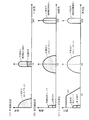
2.3 コーナ周波数
本実施形態では、周波数f1、f2、コーナ周波数fcrが例えば図6(B)、図6(C)のような関係になるように、第1型、第2型のオペアンプOP1、IP2のトランジスタのサイジングを行っている。
2.3 Corner Frequency In the present embodiment, the first-type and second-type operational amplifiers OP1 are set so that the frequencies f1 and f2 and the corner frequency fcr have a relationship as shown in FIGS. 6B and 6C, for example. IP2 transistor sizing.
即ち、第1型のオペアンプOP1では図6(B)に示すようにf1−fcr<fcr−f2の関係が成り立つようにする。一方、第2型のオペアンプOP2では図6(C)に示すようにfcr−f2<f1−fcrの関係が成り立つようにする。 That is, in the first-type operational amplifier OP1, as shown in FIG. 6B, the relationship of f1-fcr <fcr-f2 is established. On the other hand, in the second-type operational amplifier OP2, as shown in FIG. 6C, the relationship of fcr−f2 <f1−fcr is established.
なおコーナ周波数fcrは、図6(A)〜図6(C)の周波数−ノイズの特性において、フリッカノイズの特性ラインと熱ノイズの特性ラインの交点に対応する周波数である。 The corner frequency fcr is a frequency corresponding to the intersection of the flicker noise characteristic line and the thermal noise characteristic line in the frequency-noise characteristics of FIGS. 6 (A) to 6 (C).
例えば図7(A)の第1型のオペアンプOP1において、コーナ周波数fcrがE1に示す位置に設定されると、周波数f1におけるノイズが大きくなってしまい、熱ノイズを効果的に低減できない。一方、コーナ周波数fcrがE2に示す位置に設定されると、バイアス電流IBDが無駄に大きくなってしまい、低消費電力化の妨げとなる。 For example, in the first-type operational amplifier OP1 of FIG. 7A, when the corner frequency fcr is set at a position indicated by E1, noise at the frequency f1 increases, and thermal noise cannot be effectively reduced. On the other hand, when the corner frequency fcr is set to the position indicated by E2, the bias current IBD becomes unnecessarily large, which hinders low power consumption.
このため本実施形態では、第1型のオペアンプOP1については、周波数f1の近傍にコーナ周波数fcrが設定されるように、オペアンプのトランジスタのサイジングを行う。この場合に、理想的には図7(A)のE3に示すようにfcr=f1に設定することで、オペアンプの熱ノイズと消費電力を最適に小さくできる。しかしながら、fcr=f1に設定すると、プロセス変動があった場合に、熱ノイズのレベルが、所望するノイズレベルよりも大きくなってしまうおそれがある。 For this reason, in the present embodiment, for the first-type operational amplifier OP1, the transistors of the operational amplifier are sized so that the corner frequency fcr is set in the vicinity of the frequency f1. In this case, ideally, the thermal noise and power consumption of the operational amplifier can be reduced optimally by setting fcr = f1 as indicated by E3 in FIG. However, if fcr = f1 is set, the thermal noise level may become larger than the desired noise level when there is a process variation.
そこで図6(B)では、f1−fcr<fcr−f2の関係が成り立つようにして、周波数f1側にコーナ周波数fcrをなるべく近づけるようにしている。これにより、プロセス変動も考慮しながら、オペアンプのノイズ低減と低消費電力化を両立できる。 Therefore, in FIG. 6B, the relationship of f1−fcr <fcr−f2 is established, and the corner frequency fcr is set as close as possible to the frequency f1 side. As a result, it is possible to achieve both noise reduction and low power consumption of the operational amplifier while taking into account process variations.
また図7(B)の第2型のオペアンプOP2において、コーナ周波数fcrがE4に示す位置に設定されると、周波数f2におけるノイズが大きくなってしまい、フリッカノイズを効果的に低減できない。一方、コーナ周波数fcrがE5に示す位置に設定されると、WL積W1×L1が無駄に大きくなってしまい、回路の小面積化の妨げとなる。 Further, in the second-type operational amplifier OP2 of FIG. 7B, when the corner frequency fcr is set at a position indicated by E4, noise at the frequency f2 increases, and flicker noise cannot be effectively reduced. On the other hand, if the corner frequency fcr is set to the position indicated by E5, the WL product W1 × L1 becomes unnecessarily large, which hinders the reduction of the circuit area.
このため本実施形態では、第2型のオペアンプOP2については、周波数f2の近傍にコーナ周波数fcrが設定されるように、オペアンプのトランジスタのサイジングを行う。この場合に、理想的には図7(B)のE6に示すようにfcr=f2に設定することで、オペアンプのフリッカノイズとレイアウト面積を最適に小さくできる。しかしながら、fcr=f2に設定すると、プロセス変動があった場合に、フリッカノイズのレベルが、所望するノイズレベルよりも大きくなってしまうおそれがある。 Therefore, in the present embodiment, for the second-type operational amplifier OP2, the transistors of the operational amplifier are sized so that the corner frequency fcr is set in the vicinity of the frequency f2. In this case, ideally, by setting fcr = f2 as indicated by E6 in FIG. 7B, the flicker noise and layout area of the operational amplifier can be reduced optimally. However, if fcr = f2 is set, the flicker noise level may become larger than the desired noise level when there is a process variation.
そこで図6(C)では、fcr−f2<f1−fcrの関係が成り立つようにして、周波数f2側にコーナ周波数fcrをなるべく近づけるようにしている。これにより、プロセス変動も考慮しながら、オペアンプのノイズ低減と小面積化を両立できる。 Therefore, in FIG. 6C, the relationship of fcr−f2 <f1−fcr is established, and the corner frequency fcr is made as close as possible to the frequency f2. As a result, it is possible to achieve both noise reduction and area reduction of the operational amplifier while taking into account process variations.
2.4 実効ゲート電圧
図5(C)や前述の式(10)に示すように、差動段トランジスタのWL積W1b×L1bをなるべく大きくすると共に、チャネル長L1bをなるべく小さくすることで、フリッカノイズ低減できる。従って、WL比W1b/L1bが大きくなるようなサイジングを行えば、フリッカノイズを効率的に低減できると考えられる。
2.4 Effective Gate Voltage As shown in FIG. 5C and the above equation (10), flicker is achieved by increasing the WL product W1b × L1b of the differential stage transistor as much as possible and reducing the channel length L1b as much as possible. Noise can be reduced. Therefore, it is considered that flicker noise can be efficiently reduced by performing sizing such that the WL ratio W1b / L1b increases.
しかしながら、WL比W1b/L1bを大きくしすぎると、実効ゲート電圧Veffが小さくなり、かえってフリッカノイズが増加してしまうことが判明した。なお実効ゲート電圧Veffは下式(17)のように表される。 However, it has been found that if the WL ratio W1b / L1b is increased too much, the effective gate voltage Veff decreases and flicker noise increases. The effective gate voltage Veff is expressed by the following equation (17).
ここで、Vgsはトランジスタのゲート・ソース間電圧、Vthはしきい値電圧、Idsはドレイン・ソース間電流、μは移動度、Coxは単位面積当たりのゲート容量、RT1bは差動段トランジスタのWL比であり、RT1b=W1b/L1bである。 Here, Vgs is the gate-source voltage of the transistor, Vth is the threshold voltage, Ids is the drain-source current, μ is the mobility, Cox is the gate capacitance per unit area, and RT1b is the WL of the differential stage transistor. The ratio is RT1b = W1b / L1b.
例えば図8(A)、図8(B)に、実効ゲート電圧Veffとノイズ(ノイズレベルSvg)の関係についての測定結果を示す。図8(A)はN型トランジスタの例であり、図8(B)はP型トランジスタの例である。図8(A)、図8(B)では、Vgsを変化させることで実効ゲート電圧Veffを変化させている。なおドレイン・ソース間電圧Vdsはゲート・ソース間電圧Vgsと等しくなっている。 For example, FIGS. 8A and 8B show the measurement results regarding the relationship between the effective gate voltage Veff and noise (noise level Svg). FIG. 8A shows an example of an N-type transistor, and FIG. 8B shows an example of a P-type transistor. 8A and 8B, the effective gate voltage Veff is changed by changing Vgs. The drain-source voltage Vds is equal to the gate-source voltage Vgs.
図8(A)のE7、図8(B)のE8に示すように、実効ゲート電圧Veffが小さくなると、ノイズが急峻に増加している。これは、小信号振幅の基準電圧となる実効ゲート電圧Veffが小さくなると、トランジスタが弱反転領域で動作するようになり、フリッカノイズが急激に増加することに起因する。例えば図8(A)、図8(B)ではVeff=10mV〜100mVからフリッカノイズが急激に増加している。従って、弱反転領域での動作に起因するフリッカノイズの増加を抑えるためには、実効ゲート電圧Veffを10mV〜100mVよりも大きくすることが望ましい。 As indicated by E7 in FIG. 8A and E8 in FIG. 8B, when the effective gate voltage Veff decreases, the noise increases sharply. This is because when the effective gate voltage Veff, which is a reference voltage having a small signal amplitude, decreases, the transistor operates in the weak inversion region, and flicker noise increases rapidly. For example, in FIGS. 8A and 8B, the flicker noise increases rapidly from Veff = 10 mV to 100 mV. Therefore, in order to suppress an increase in flicker noise resulting from the operation in the weak inversion region, it is desirable that the effective gate voltage Veff be larger than 10 mV to 100 mV.
図9(A)は、実効ゲート電圧Veffを変化させたときのオペアンプの面積と消費電流とノイズの関係を示すシミュレーション結果であり、X軸が面積(オペアンプを正方形とした場合の一辺の長さ)を表し、Y軸が消費電流を表し、Z軸がノイズレベルを表す。 FIG. 9A is a simulation result showing the relationship between the area of the operational amplifier, the current consumption, and the noise when the effective gate voltage Veff is changed. The X axis is the area (the length of one side when the operational amplifier is square). ), The Y axis represents the current consumption, and the Z axis represents the noise level.
図9(A)ではWL積W1b×L1bが一定の条件で、WL比RT1b=W1b/L1bを変化させることで、実効ゲート電圧Veffを変化させている。例えば図9(A)のF1、F2に示す矢印の方向が、実効ゲート電圧Veffが小さくなる方向であり、WL比RT1b=W1b/L1bを大きくすることで、実効ゲート電圧Veffを小さくしている。 In FIG. 9A, the effective gate voltage Veff is changed by changing the WL ratio RT1b = W1b / L1b under the condition that the WL product W1b × L1b is constant. For example, the directions indicated by arrows F1 and F2 in FIG. 9A are directions in which the effective gate voltage Veff decreases, and the effective gate voltage Veff is decreased by increasing the WL ratio RT1b = W1b / L1b. .
図9(A)のF1に示すように、実効ゲート電圧Veffが小さくなると、オペアンプの面積が小さくなると共に消費電流も小さくなるが、ノイズについてはほとんど変化しない。 As indicated by F1 in FIG. 9A, when the effective gate voltage Veff is reduced, the area of the operational amplifier is reduced and the current consumption is reduced, but the noise is hardly changed.
ところが図9(A)のF3においてノイズが急激に増加している。即ちWL比RT1b=W1b/L1bが所定値よりも大きくなると、図8(A)、図8(B)で説明したようにトランジスタが弱反転領域で動作することでフリッカノイズが急激に増加し、オペアンプのノイズも急激に増加する。 However, the noise increases rapidly at F3 in FIG. That is, when the WL ratio RT1b = W1b / L1b becomes larger than a predetermined value, the flicker noise increases abruptly because the transistor operates in the weak inversion region as described with reference to FIGS. 8A and 8B. The noise of the operational amplifier also increases rapidly.
この場合、図9(A)のF4のポイントでは、ノイズは小さいものの、オペアンプの面積や消費電流は大きいため、面積や電流が無駄に消費されている。 In this case, at the point F4 in FIG. 9A, although the noise is small, the area and current consumption of the operational amplifier are large, so that the area and current are wasted.
そこで本実施形態では、図9(A)のF3のポイントに設定されるように、差動段トランジスタのWL比RT1b=W1b/L1bを決める(値を絞り込む)。例えばWL比RT1bは50〜200の範囲の中の値とすることができる。そしてこのようにして決められたRT1bの条件の下で、図5(C)のようにW1b×L1bが大きくなると共にL1b/L3bが小さくなるように、オペアンプのトランジスタのサイジングを行う。 Therefore, in the present embodiment, the WL ratio RT1b = W1b / L1b of the differential stage transistor is determined (the value is narrowed down) so as to be set to the point F3 in FIG. 9A. For example, the WL ratio RT1b can be a value in the range of 50 to 200. Then, under the condition of RT1b determined in this way, the transistors of the operational amplifier are sized so that W1b × L1b becomes larger and L1b / L3b becomes smaller as shown in FIG. 5C.
具体的にはトランジスタが弱反転領域で動作しないようにするためには、下式(18)が成り立てばよい。 Specifically, in order to prevent the transistor from operating in the weak inversion region, the following equation (18) may be established.
ここで、kはボルツマン定数、Tは絶対温度、q(=1.602×10⁻¹⁹クーロン)は電子電荷量であり、室温(25度)では、k×T/q=25.7mVになる。 Here, k is a Boltzmann constant, T is an absolute temperature, q (= 1.602 × 10 −19 coulomb) is an electronic charge amount, and k × T / q = 25.7 mV at room temperature (25 degrees). .
但し図8(A)、図8(B)に示すように、弱反転領域と強反転領域の境界においてもフリッカノイズが上昇しており、プロセス変動を考慮する必要がある。そこでプロセス変動パラメータ(プロセス依存パラメータ)をP(P>1)とした場合に、下式(19)が成り立つようにする。 However, as shown in FIGS. 8A and 8B, flicker noise also rises at the boundary between the weak inversion region and the strong inversion region, and it is necessary to consider process variation. Therefore, when the process variation parameter (process-dependent parameter) is P (P> 1), the following equation (19) is established.
ここで、プロセス変動パラメータは例えばP=3.0とすることができ、更に望ましくはPは1.5〜2.0の範囲の値とすることができる。 Here, the process variation parameter can be, for example, P = 3.0, and more preferably, P can be a value in the range of 1.5 to 2.0.
本実施形態では上式(19)を満たす範囲の実効ゲート電圧Veffになるように、差動段トランジスタのWL比RT1b=W1b/L1bを決める。そして、決められたRT1bの範囲の下で、W1b×L1bが大きくなると共にL1b/L3bが小さくなるように、オペアンプのトランジスタのサイジングを行う。なお、W1b/L1bを決めて、W1b×L1bやL1b/L3bを決めた後に、再度、RT1bを変化させて、微調整を行うことが望ましい。 In this embodiment, the WL ratio RT1b = W1b / L1b of the differential stage transistor is determined so that the effective gate voltage Veff is in a range satisfying the above equation (19). Then, the transistors of the operational amplifier are sized so that W1b × L1b becomes larger and L1b / L3b becomes smaller under the determined RT1b range. It should be noted that after W1b / L1b is determined and W1b × L1b or L1b / L3b is determined, RT1b is changed again to perform fine adjustment.
なお図9(B)は、差動段トランジスタのゲート長L1bと能動負荷段トランジスタのゲート長L3bの比であるL1b/L3b(別の言い方をすればL3b/L1b)を変化させたときのオペアンプの面積と消費電流とノイズの関係を示すシミュレーション結果である。 FIG. 9B shows an operational amplifier when L1b / L3b (in other words, L3b / L1b), which is the ratio of the gate length L1b of the differential stage transistor and the gate length L3b of the active load stage transistor, is changed. It is a simulation result which shows the relationship of an area, current consumption, and noise.
図9(B)のF5に示すようにL1b/L3bを大きくして行くと(L3b/L1bを小さくして行くと)、F6に示すポイントからF7に示すようにノイズが急激に増加する。この場合、L1b/L3bを大きくして行くと、オペアンプの面積は小さくなるが、消費電流はほとんど変化しないことがわかる。 When L1b / L3b is increased as indicated by F5 in FIG. 9B (L3b / L1b is decreased), the noise increases rapidly from the point indicated by F6 as indicated by F7. In this case, as L1b / L3b is increased, the area of the operational amplifier is reduced, but the consumption current hardly changes.
図9(B)の結果から、L1b/L3bを最適に設定するためには、F6に示すポイントになるようにL1b/L3bを設定すればよいことがわかる。具体的にはL1b/L3bの比は、例えば0.4〜0.8の範囲内の値にすることができる。 From the result of FIG. 9B, it can be seen that in order to optimally set L1b / L3b, it is only necessary to set L1b / L3b so as to be the point indicated by F6. Specifically, the ratio of L1b / L3b can be set to a value within the range of 0.4 to 0.8, for example.
本実施形態では以上のようにオペアンプのトランジスタのサイジングを行うことで、ノイズ低減と回路の小規模化や低消費電力化との両立に成功している。 In the present embodiment, by sizing the transistors of the operational amplifier as described above, it is possible to achieve both noise reduction, circuit scale reduction, and low power consumption.
例えば基準電圧供給回路20は、第1の回路310、第2の回路320に対してAGND(アナログ基準電圧)を供給する。このAGNDはアナログ回路の基準となる電圧であり、オペアンプの信号増幅はこのAGNDを基準として行われる。従って、基準電圧供給回路20は、安定した電位のAGNDを第1の回路310、第2の回路320に供給する必要がある。
For example, the reference
一方、第1の回路310は、第1型のオペアンプOP1により構成することが望ましく、第2の回路320は、第2型のオペアンプOP2により構成することが望ましい。例えば第1の回路310を熱ノイズ低減重視の第1型のオペアンプOP1により構成すれば、第1の回路310のノイズを低減できる。また第2の回路320を、フリッカノイズ低減重視の第2型のオペアンプOP2により構成すれば、第2の回路320のノイズを低減できる。
On the other hand, the
しかしながら、このように第1の回路310を第1型のオペアンプOP1により構成し、第2の回路320を第2型のオペアンプOP2により構成したとしても、基準電圧供給回路20により供給されるAGNDに熱ノイズやフリッカノイズが重畳されると、システム全体のSNRの向上が難しくなるということが判明した。
However, even if the
例えば第1の供給回路21からのAGNDが供給されて動作する第1の回路310では、増幅対象信号の周波数f1は図5(A)に示すように高い周波数になっており、この周波数f1では前述のように熱ノイズが支配的になっている。従って、第1の回路310として第1型のオペアンプを用いたとしても、第1の供給回路21からのAGNDに熱ノイズが重畳されてしまうと、結局、第1の回路310の熱ノイズが増加する。
For example, in the
この点、本実施形態では、第1の供給回路21が、基準電圧用の第1型のオペアンプOP1を有し、このOP1を用いてAGNDを供給している。そしてこの基準電圧用の第1型のオペアンプOP1は、図5(C)等で説明したように、熱ノイズ低減重視のオペアンプとなっている。従って、AGND線AGL1に重畳される熱ノイズを最小限に抑えることができ、第1の回路310での熱ノイズの増加を防止できる。
In this regard, in the present embodiment, the
また第2の供給回路22からのAGNDが供給されて動作する第2の回路320では、増幅対象信号の周波数f2は図5(A)に示すように低い周波数になっており、この周波数f2では前述のようにフリッカノイズが支配的になっている。従って、第2の回路320として第2型のオペアンプを用いたとしても、第2の供給回路22からのAGNDにフリッカノイズが重畳されてしまうと、結局、第2の回路320のフリッカノイズが増加する。
Further, in the
この点、本実施形態では、第2の供給回路22が、基準電圧用の第2型のオペアンプOP2を有し、このOP2を用いてAGNDを供給している。そしてこの基準電圧用の第2型のオペアンプOP2は、図5(C)等で説明したように、フリッカノイズ低減重視のオペアンプとなっている。従って、AGND線AGL2に重畳されるフリッカノイズを最小限に抑えることができ、第2の回路320でのフリッカノイズの増加を防止できる。
In this regard, in the present embodiment, the
なお第1の供給回路21からのAGNDはAGND線AGL1(広義には第1のアナログ基準電圧線)を介して供給される。一方、第2の供給回路22からのAGNDはAGND線AGL2(広義には第2のアナログ基準電圧線)を介して供給される。この場合に、AGND線AGL1とAGL2とが、基準電圧供給回路20から第1、第2の回路310、320に対して分離されて配線される。即ち2本のAGND線AGL1、AGL2が、レイアウト的に分離されて、第1の回路310、第2の回路320に接続される。このようにすることで、AGND線AGL1からのノイズがAGND線AGL2に伝達されたり、AGND線AGL2からのノイズがAGND線AGL1に伝達される事態を防止できる。
The AGND from the
例えばAGND線AGL2からの熱ノイズがAGND線AGL1に伝達されてしまうと、第1の供給回路21に熱ノイズ低減重視の第1型のオペアンプOP1を使用したとしても、AGL2からの熱ノイズが第1の回路310に伝達されてしまい、SNRが劣化する。同様に、AGND線AGL1からのフリッカノイズがAGND線AGL2に伝達されてしまうと、第2の供給回路22にフリッカノイズ低減重視の第2型のオペアンプOP2を使用したとしても、AGL1からのフリッカノイズが第2の回路320に伝達されてしまい、SNRが劣化する。
For example, if thermal noise from the AGND line AGL2 is transmitted to the AGND line AGL1, even if the first-type operational amplifier OP1 that emphasizes thermal noise reduction is used in the
この点、AGND線AGL1、AGL2をレイアウト的に分離して配線すれば、上記のような事態の発生を防止でき、システム全体のSNRを向上できる。 In this regard, if the AGND lines AGL1 and AGL2 are separated and wired in the layout, the above situation can be prevented and the SNR of the entire system can be improved.
図10は、後述するジャイロセンサの検出装置に本実施形態の手法を適用した場合の結果であり、QVAMP、DIFF、PGA、SYNCD、FLTは、各々、Q/V変換回路、差動増幅回路、感度調整回路、同期検波回路、フィルタ部のノイズレベルを示す。 FIG. 10 shows the results when the method of the present embodiment is applied to a gyro sensor detection device to be described later. QVAMP, DIFF, PGA, SYNCD, and FLT are a Q / V conversion circuit, a differential amplification circuit, The noise level of a sensitivity adjustment circuit, a synchronous detection circuit, and a filter part is shown.
図10に示すように本実施形態によれば、AC信号を扱う第1の回路310に対してAGNDを供給する第1の供給回路21と、DC信号を扱う第2の回路320に対してAGNDを供給する第2の供給回路22のそれぞれについて、オペアンプを使い分け、最適な低ノイズ設計を行った結果、システム全体を効率良く低ノイズ化することに成功している。
As shown in FIG. 10, according to the present embodiment, the
2.5 レイアウト
次に、第1型、第2型のオペアンプOP1、OP2のレイアウト手法について説明する。図11(A)は第1型のオペアンプOP1のレイアウト例であり、図11(B)は第2型のオペアンプOP2のレイアウト例である。
2.5 Layout Next, a layout method of the first-type and second-type operational amplifiers OP1 and OP2 will be described. FIG. 11A is a layout example of the first-type operational amplifier OP1, and FIG. 11B is a layout example of the second-type operational amplifier OP2.
図11(B)において、H2は、第2型のオペアンプOP2を構成する素子(トランジスタ、キャパシタ又は抵抗等)のうち差動段トランジスタM1、M2の配置領域を示している。このH2の配置領域の面積をSdfとし、第2型のオペアンプを構成する素子のうち差動段トランジスタM1、M2以外の素子の配置領域の面積をSreとする。なお差動段トランジスタM1、M2以外の素子とは、例えば図4(A)のM1、M2以外のトランジスタM3、M4、M5、M6、M7や、キャパシタCF、抵抗RFなどである。この場合に図11(B)では、Sdf>Sreの関係が成り立つ。このような関係が成り立てば、WL積W1b×L1bを大きくすることができ、フリッカノイズを低減できる。 In FIG. 11B, H2 indicates an arrangement region of the differential stage transistors M1 and M2 among the elements (transistors, capacitors, resistors, etc.) constituting the second-type operational amplifier OP2. The area of the arrangement region of H2 is Sdf, and the area of the arrangement region of elements other than the differential stage transistors M1 and M2 among the elements constituting the second-type operational amplifier is Sre. The elements other than the differential stage transistors M1 and M2 are, for example, transistors M3, M4, M5, M6, and M7 other than M1 and M2 in FIG. 4A, a capacitor CF, and a resistor RF. In this case, in FIG. 11B, a relationship of Sdf> Sre is established. If such a relationship is established, the WL product W1b × L1b can be increased, and flicker noise can be reduced.
一方、図11(A)の第1型のオペアンプOP1では、H1に示すように差動段トランジスタM1、M2の配置領域は小さいため、Sdf>Sreの関係は成り立たない。その代わりに、バイアス電流IBD=Iaが大きくなるようなトランジスタのサイジングを行うことで、熱ノイズを低減している。 On the other hand, in the first-type operational amplifier OP1 in FIG. 11A, since the arrangement region of the differential stage transistors M1 and M2 is small as indicated by H1, the relationship of Sdf> Sre does not hold. Instead, thermal noise is reduced by sizing the transistor so that the bias current IBD = Ia is increased.
また図11(B)では、第2型のオペアンプOP2の差動段トランジスタM1は、並列接続された複数(J個)のトランジスタTR11、TR12、TR13、TR14により構成される。同様にOP2の差動段トランジスタM2は、並列接続された複数のトランジスタTR21、TR22、TR23、TR24により構成される。そしてH2に示す差動段トランジスタM1、M2の配置領域には、このように並列接続された複数のトランジスタTR11〜TR14やTR21〜TR24が配置される。 In FIG. 11B, the differential stage transistor M1 of the second-type operational amplifier OP2 includes a plurality (J) of transistors TR11, TR12, TR13, and TR14 connected in parallel. Similarly, the differential stage transistor M2 of OP2 includes a plurality of transistors TR21, TR22, TR23, and TR24 connected in parallel. A plurality of transistors TR11 to TR14 and TR21 to TR24 connected in parallel are arranged in the arrangement region of the differential stage transistors M1 and M2 indicated by H2.
図11(B)ではX方向がチャネル長の方向となり、Y方向がチャネル幅の方向になる。そして並列接続されたTR11〜TR14やTR21〜TR24の各トランジスタのチャネル長はL1bになる。一方、並列接続されたTR11〜TR14やTR21〜TR24のトランジスタの個数をJ個(図11(B)ではJ=4)とすると、TR11〜TR14やTR21〜TR24の各トランジスタのチャネル幅はW11b=W1b/Jになる。 In FIG. 11B, the X direction is the channel length direction, and the Y direction is the channel width direction. The channel lengths of the transistors TR11 to TR14 and TR21 to TR24 connected in parallel are L1b. On the other hand, if the number of transistors TR11 to TR14 and TR21 to TR24 connected in parallel is J (J = 4 in FIG. 11B), the channel width of each transistor of TR11 to TR14 and TR21 to TR24 is W11b = W1b / J.
図11(B)のように並列接続されたトランジスタTR11〜TR14やTR21〜TR24を配置するようにすれば、WL積W1b×L1bを大きくしながらWL比W1b/L1bも大きくできるようになり、フリッカノイズを効率的に低減できる。 If the transistors TR11 to TR14 and TR21 to TR24 connected in parallel as shown in FIG. 11B are arranged, the WL ratio W1b / L1b can be increased while the WL product W1b × L1b is increased, and the flicker is increased. Noise can be reduced efficiently.
なお図11(B)では、能動負荷段トランジスタM3やM4も、並列接続された複数(I個)のトランジスタTR31、TR32やTR41、TR42により構成される。そして並列接続されたTR31、TR32やTR41、TR42の各トランジスタのチャネル長はL3bになる。一方、並列接続されたトランジスタTR31、TR32やTR41、TR42の個数をI個(図11(B)ではI=2)とすると、TR31、TR32やTR41、TR42の各トランジスタのチャネル幅はW33b=W3b/Iとなる。 In FIG. 11B, the active load stage transistors M3 and M4 are also composed of a plurality (I pieces) of transistors TR31, TR32, TR41, and TR42 connected in parallel. The channel length of each transistor of TR31, TR32, TR41, and TR42 connected in parallel is L3b. On the other hand, if the number of transistors TR31, TR32, TR41, TR42 connected in parallel is I (I = 2 in FIG. 11B), the channel width of each transistor of TR31, TR32, TR41, TR42 is W33b = W3b. / I.
そして図11(B)では、差動段トランジスタM1やM2の配置領域では、X方向にJ個(例えばJ=4)のトランジスタTR11〜TR14やTR21〜TR24が配置される一方で、能動負荷段トランジスタM3やM4の配置領域では、X方向にI個(I<J。例えばI=2)のトランジスタTR31、TR32やTR41、TR42が配置される。このようにすれば、図5(C)で説明したL1b<L3bの関係を満たしながら、M1、M2を構成するトランジスタTR11〜TR14、TR21〜TR24や、M3、M4を構成するトランジスタTR31〜TR32、TR41〜TR42を、矩形の配置領域に効率良く対称配置できる。これにより、レイアウト効率を向上できる。 In FIG. 11B, J (for example, J = 4) transistors TR11 to TR14 and TR21 to TR24 are arranged in the X direction in the arrangement region of the differential stage transistors M1 and M2, while the active load stage. In the arrangement region of the transistors M3 and M4, I (I <J, for example, I = 2) transistors TR31, TR32, TR41, and TR42 are arranged in the X direction. In this way, while satisfying the relationship of L1b <L3b described in FIG. 5C, the transistors TR11 to TR14, TR21 to TR24 that constitute M1 and M2, and the transistors TR31 to TR32 that constitute M3 and M4, TR41 to TR42 can be efficiently arranged symmetrically in a rectangular arrangement region. Thereby, layout efficiency can be improved.
図12に第3型のオペアンプOP3のレイアウト例を示す。図12においてH3は、差動段トランジスタM1、M2の配置領域を示している。図12においても図11(B)と同様にSdf>Sreの関係が成り立っており、WL積W1c×L1cを大きくすることができるため、フリッカノイズを低減できる。 FIG. 12 shows a layout example of the third-type operational amplifier OP3. In FIG. 12, H3 indicates an arrangement region of the differential stage transistors M1 and M2. In FIG. 12, the relationship of Sdf> Sre is established as in FIG. 11B, and the WL product W1c × L1c can be increased, so that flicker noise can be reduced.
また図12においても、差動段トランジスタM1やM2は、並列接続された複数のトランジスタTS11〜TS14やTS21〜TS24により構成される。そしてH3に示す差動段トランジスタM1、M2の配置領域には、このように並列接続された複数(J個)のトランジスタTS11〜TS14やTS21〜TS24が配置されている。 Also in FIG. 12, the differential stage transistors M1 and M2 are constituted by a plurality of transistors TS11 to TS14 and TS21 to TS24 connected in parallel. A plurality (J) of the transistors TS11 to TS14 and TS21 to TS24 connected in parallel are arranged in the arrangement region of the differential stage transistors M1 and M2 indicated by H3.
そして並列接続されたTS11〜TS14やTS21〜TS24の各トランジスタのチャネル長はL1cになり、チャネル幅はW11c=W1c/Jとなる。 The channel length of the transistors TS11 to TS14 and TS21 to TS24 connected in parallel is L1c, and the channel width is W11c = W1c / J.
図12と図11(B)を比較すれば明らかなように、図12の第3型のオペアンプOP3では、H3に示す差動段トランジスタM1、M2の配置領域の面積が図11(B)よりも更に大きくなっている。これにより、フリッカノイズを図11(B)よりも更に低減できるオペアンプを実現できる。 As apparent from a comparison between FIG. 12 and FIG. 11B, in the third-type operational amplifier OP3 in FIG. 12, the area of the arrangement region of the differential stage transistors M1 and M2 indicated by H3 is larger than that in FIG. Is even larger. Thus, an operational amplifier that can further reduce flicker noise than that in FIG. 11B can be realized.
2.6.基準電圧供給回路
図13に基準電圧供給回路20の詳細な構成例を示す。なお基準電圧供給回路20は図13の構成に限定されず、その構成要素の一部を省略したり、他の構成要素を追加するなどの種々の変形実施が可能である。
2.6. Reference Voltage Supply Circuit FIG. 13 shows a detailed configuration example of the reference
基準電圧供給回路20は第1、第2、第3の供給回路21、22、23を含む。また基準電圧発生回路26を含む。
The reference
第1の供給回路21(第1のインピーダンス変換回路)は、例えば基準電圧用の第1型のオペアンプOP1を用いて、電圧のインピーダンス変換を行う。即ち、第1の供給回路21が含む第1型のオペアンプOP1は、その反転入力端子(広義には第2の入力端子)が出力端子に接続されたボルテージフォロワ接続のオペアンプになっており、OP1の出力端子はAGND線AGL1に接続されている。
The first supply circuit 21 (first impedance conversion circuit) performs voltage impedance conversion using, for example, a first-type operational amplifier OP1 for reference voltage. That is, the first-type operational amplifier OP1 included in the
また第2の供給回路22(第2のインピーダンス変換回路)は、例えば基準電圧用の第2型のオペアンプOP2を用いて、電圧のインピーダンス変換を行う。即ち、第2の供給回路22が含む第2型のオペアンプOP2は、その反転入力端子(第2の入力端子)が出力端子に接続されたボルテージフォロワ接続のオペアンプになっており、OP2の出力端子はAGND線AGL2に接続されている。
The second supply circuit 22 (second impedance conversion circuit) performs voltage impedance conversion using, for example, a second-type operational amplifier OP2 for reference voltage. That is, the second-type operational amplifier OP2 included in the
第3の供給回路23は、第1、第2の供給回路21、22の前段側に設けられ、第1、第2の供給回路21、22に対して出力電圧V3Qを供給する。例えば第1、第2の供給回路21、22は、第3の供給回路23からの出力電圧V3Qのインピーダンス変換を行って、AGNDを出力する。
The
第3の供給回路23は、図5(C)、図12で説明した第3型のオペアンプOP3を含む。また抵抗RJ1、RJ2、RJ3により構成される電圧分割回路を含むことができる。
The
基準電圧発生回路26は、AGNDを生成するための基準電圧VRを発生する。この基準電圧発生回路26としては、例えばバンドギャップにより基準電圧VRを発生する回路を採用できる。
The reference
例えば図13において、ノードNJ1の電圧は、第3型のオペアンプOP3のイマジナリーショートにより、基準電圧VRと等しくなる。従って、抵抗RJ2、RJ3の抵抗値をR2、R3とすると、第3の供給回路23の出力電圧はV3Q=VR×{(R2+R3)/R3}となる。第1、第2の供給回路21、22は、この出力電圧V3Q=AGND=VR×{(R2+R3)/R3}の電圧のインピーダンス変換を行う。これによりAGNDの電位安定化が図られる。
For example, in FIG. 13, the voltage at the node NJ1 becomes equal to the reference voltage VR due to an imaginary short of the third-type operational amplifier OP3. Therefore, when the resistance values of the resistors RJ2 and RJ3 are R2 and R3, the output voltage of the
さて、基準電圧用の第3型のオペアンプOP3の差動部の差動段トランジスタのチャネル幅をW1cとし、チャネル長をL1cとし、差動部に流れるバイアス電流をIcとしたとする。この場合に、W1c×L1c>W1a×L1a、Ic>Ibの関係が成り立つようになっている。 Now, suppose that the channel width of the differential stage transistor in the differential section of the third-type operational amplifier OP3 for reference voltage is W1c, the channel length is L1c, and the bias current flowing in the differential section is Ic. In this case, the relationship of W1c × L1c> W1a × L1a and Ic> Ib is established.
即ち第1の供給回路21は、第3の供給回路23からの出力電圧V3Qを受けて、AGNDを増幅回路70に供給する。従って、第3の供給回路23の出力電圧V3Qに熱ノイズが重畳されると、第1の供給回路21として熱ノイズ低減重視の第1型のオペアンプOP1を用いたとしても、V3Qに重畳された熱ノイズが第1の回路310に伝達されてしまう。この結果、システム全体のSNRが劣化する。
That is, the
また第2の供給回路22は、第3の供給回路23からの出力電圧V3Qを受けて、AGNDをフィルタ部110に供給する。従って、第3の供給回路23の出力電圧V3Qにフリッカノイズが重畳されると、第2の供給回路22としてフリッカノイズ低減重視の第2型のオペアンプOP2を用いたとしても、V3Qに重畳されたフリッカノイズが第2の回路320に伝達されてしまう。この結果、システム全体のSNRが劣化する。
The
この点、図13の第3の供給回路23の第3型のオペアンプOP3では、W1c×L1c>W1a×L1a、Ic>Ibの関係が成り立つ。更に望ましくは、W1c×L1c>W1b×L1b、Ic>Iaの関係が成り立つ。従って、第3型のオペアンプOP3は、熱ノイズ及びフリッカノイズの両方が低いオペアンプとなる。例えば第3の型のオペアンプOP3は、図12のレイアウト例に示すように、WL積も大きく、バイアス電流も大きい。従って、熱ノイズ及びフリッカノイズの両方において非常に低ノイズなオペアンプになる。
In this regard, in the third-type operational amplifier OP3 of the
このように、第3の供給回路23として熱ノイズ及びフリッカノイズの両方において低ノイズな第3型のオペアンプOP3を用いれば、第3の供給回路23の出力電圧V3Qの熱ノイズ及びフリッカノイズを最小限に抑えることができる。従って、出力電圧V3Qの熱ノイズが第1の供給回路21を介して第1の回路310に伝達したり、出力電圧V3Qのフリッカノイズが第2の供給回路22を介して第2の回路320に伝達する事態を、最小限に抑えることが可能になり、システム全体のSNRを大幅に向上できる。
As described above, when the third-type operational amplifier OP3 having low noise in both thermal noise and flicker noise is used as the
3.ジャイロセンサの検出装置への適用
3.1 検出装置の構成
次に、本実施形態の手法をジャイロセンサの検出装置に適用した場合について説明する。図14に本実施形態の手法が適用される検出装置30の構成例を示す。この検出装置30は駆動回路40と検出回路60を含む。なお検出装置30は図14の構成に限定されず、その構成要素の一部を省略したり、他の構成要素を追加するなどの種々の変形実施が可能である。例えば、振動子10からの検出信号に基づいて同期信号を抽出できる場合等には、駆動回路40の構成を省略してもよい。
3. Application of Gyro Sensor to Detection Device 3.1 Configuration of Detection Device Next, a case where the method of the present embodiment is applied to a detection device of a gyro sensor will be described. FIG. 14 shows a configuration example of the
物理量トランスデューサである振動子10(振動ジャイロ)は、例えば水晶などの圧電材料により形成される圧電振動子である。図15(A)に、振動子10の一例として音叉型圧電振動子を示す。この振動子10は、駆動用振動子11、12と検出用振動子16、17を含む。駆動用振動子11、12には駆動端子2、4が設けられ、検出用振動子16、17には検出端子6、8が設けられている。なお図15(A)では、振動子10が音叉型である場合の例を示しているが、本実施形態の振動子10はこのような構造に限定されない。例えばT字型やダブルT字型等であってもよい。また振動子10の圧電材料は水晶以外であってもよい。また物理量トランスデューサである振動子10は、静電容量による駆動・検出動作を同様に行う静電型MEMS(Micro Electro Mechanical Systems)であってもよい。また物理量トランスデューサとは物理量(物の性質の度合いを表す量であり、その単位が定義されているもの)を他の物理量に変換するための素子である。変換対象となる物理量としては、コリオリ力以外にも重力などの力や、加速度、質量などが考えられる。また変換により得られる物理量としては、電流(電荷)以外にも電圧等であってもよい。
The vibrator 10 (vibration gyro), which is a physical quantity transducer, is a piezoelectric vibrator formed of a piezoelectric material such as quartz. FIG. 15A shows a tuning fork type piezoelectric vibrator as an example of the
駆動回路40は、駆動信号(駆動電圧)VDを出力して振動子10(広義には物理量トランスデューサ)を駆動し、振動子10からフィードバック信号VFを受ける。これにより振動子10を励振させる。検出回路60は、駆動信号VDにより駆動される振動子10から検出信号(検出電流、電荷)ISP、ISMを受け、検出信号から所望信号(コリオリ力信号)を検出(抽出)する。
The
具体的には、駆動回路40からの交流の駆動信号(駆動電圧)VDが図15(A)の駆動用振動子11の駆動端子2に印加される。すると逆電圧効果によって駆動用振動子11が振動を開始し、音叉振動により駆動用振動子12も振動を開始する。この時、駆動用振動子12の圧電効果によって発生する電流(電荷)が、駆動端子4からフィードバック信号VFとして駆動回路40にフィードバックされる。これにより振動子10を含む発振ループが形成される。
Specifically, an alternating drive signal (drive voltage) VD from the
駆動用振動子11、12が振動すると、検出用振動子16、17が図15(A)に示す方向に振動速度vで振動する。すると、検出用振動子16、17の圧電効果によって発生する電流(電荷)が、検出信号ISP、ISMとして検出端子6、8から出力される。検出回路60は、これらの検出信号ISP、ISMを受け、コリオリ力に応じた信号である所望信号(所望波)を検出する。
When the
即ち、図15(A)の検出軸19を中心に振動子10(ジャイロセンサ)が回転すると、振動速度vの振動方向と直交する方向にコリオリ力Fcが発生する。例えば図15(B)に、図15(A)の検出軸19を上側から見た図を模式的に示す。図15(B)において、検出軸19を中心に回転したときの角速度をωとし、振動子の質量をmとし、振動子の振動速度をvとすると、コリオリ力はFc=2m・v・ωと表される。従って検出回路60が、コリオリ力に応じた信号である所望信号を検出(抽出)することで、ジャイロセンサ(振動子)の回転角速度ωを求めることができる。
That is, when the vibrator 10 (gyro sensor) rotates around the
なお振動子10には、駆動側共振周波数fdと検出側共振周波数fsがある。具体的には、駆動用振動子11、12の固有共振周波数(駆動振動モードの固有共振周波数)がfdであり、検出用振動子16、17の固有共振周波数(検出振動モードの固有共振周波数)がfsである。この場合に、駆動用振動子11、12と検出用振動子16、17とが検出動作可能で、且つ、不要な共振結合を起こさない適度なモード間結合を持つ範囲で、fdとfsの間に一定の周波数差を持たせている。この周波数差である離調周波数Δf=|fd−fs|は、fd、fsに比べて十分に小さな周波数に設定されている。
The
駆動回路(発振回路)40は、増幅回路42と、自動ゲイン制御を行うAGC(Automatic Gain Control)回路44と、2値化回路(コンパレータ)46を含む。駆動回路40では、ジャイロセンサの感度を一定に保つために、振動子10(駆動用振動子)に供給する駆動電圧の振幅を一定に保つ必要がある。このため、駆動振動系の発振ループ内に、ゲインを自動調整するためのAGC回路44が設けられる。具体的にはAGC回路44は、フィードバック信号FDの振幅(振動子の振動速度v)が一定になるように、ゲインを可変に自動調整する。なお、発振ループでの位相シフトが0度(0deg)になるように位相が調整される。また発振起動時には、高速な発振起動を可能にするために、発振ループのゲインは1よりも大きなゲインに設定される。
The drive circuit (oscillation circuit) 40 includes an
増幅回路42は、振動子10からのフィードバック信号FDを増幅する。具体的には増幅回路42が含むI/V変換回路が、振動子10からのフィードバック信号FDである電流(電荷)を、電圧に変換して増幅し、駆動側増幅信号VD2として出力する。
The
AGC回路44は、駆動側の増幅回路42により増幅された後の信号である駆動側増幅信号VD2を監視して、発振ループのゲインを制御する。このAGC回路44は、発振ループ内の発振振幅を制御するためのゲインコントロールアンプ(GCA)や、発振振幅に応じてゲインコントロールアンプのゲインを調整するための制御電圧を出力するゲイン制御回路を含むことができる。また、このゲイン制御回路は、増幅回路42からの交流の信号VD2を直流信号に変換する整流回路(全波整流回路)や、整流回路からの直流信号の電圧と基準電圧との差分に応じた制御電圧を出力する回路などを含むことができる。
The
2値化回路46は、正弦波である駆動側増幅信号VD2の2値化処理を行い、2値化処理により得られた同期信号(参照信号)CLKを、検出回路60の同期検波回路100に出力する。この2値化回路46は、増幅回路42からの正弦波(交流)の信号VD2が入力されて、矩形波の同期信号CLKを出力するコンパレータにより実現できる。なお増幅回路42と2値化回路46の間や2値化回路46と同期検波回路100の間に他の回路を設けてもよい。例えばハイパスフィルタや移相回路(位相シフタ)などを設けてもよい。
The
検出回路60は、増幅回路70、同期検波回路100、フィルタ部110を含む。なおこれらの一部の構成要素を省略したり、他の構成要素を追加してもよい。
The
増幅回路70は、振動子10からの検出信号ISP、ISMを増幅する。具体的には増幅回路70が含むQ/V変換回路(I/V変換回路)が、振動子10からの信号ISP、ISMを受け、振動子10で発生した電荷(電流)を電圧に変換して増幅する。
The
同期検波回路(検波回路、検波器)100は、同期信号(同期クロック、参照信号)CLKに基づいて同期検波を行う。この同期検波により、機械振動漏れの不要信号の除去が可能になる。 A synchronous detection circuit (detection circuit, detector) 100 performs synchronous detection based on a synchronous signal (synchronous clock, reference signal) CLK. This synchronous detection makes it possible to eliminate unnecessary signals for mechanical vibration leakage.
同期検波回路100の後段側に設けられるフィルタ部110は、同期検波後の信号VS6のフィルタ処理を行う。具体的には、高周波成分を除去するローパスフィルタ処理を行う。
The
振動子10からの検出信号(センサ信号)には、所望信号(所望波)と不要信号(不要波)が混在している。不要信号の振幅は一般的に所望信号の振幅の100〜500倍程度となるため、検出装置30に対する要求性能は高くなる。この不要信号には、機械振動漏れや、静電結合漏れや、離調周波数Δfや、2fd(2ωd)や、DCオフセットなどに起因するものがある。機械振動漏れの不要信号は、振動子10の形状のアンバランス等に起因して発生する。また静電結合漏れの不要信号は、図14の駆動信号VDが、寄生キャパシタCP、CMを通じてISP、ISMの入力端子等に漏洩することで発生する。
The detection signal (sensor signal) from the
図16(A)〜図16(C)は、不要信号の除去について説明するための周波数スペクトラムである。図16(A)は同期検波前の周波数スペクトラムである。図16(A)に示すように、同期検波前の検出信号では、DCの周波数帯域にはDCオフセットの不要信号が存在する。またfdの周波数帯域には、機械振動漏れの不要信号と所望信号が存在する。 FIG. 16A to FIG. 16C are frequency spectra for explaining the removal of unnecessary signals. FIG. 16A shows a frequency spectrum before synchronous detection. As shown in FIG. 16A, in the detection signal before synchronous detection, there is a DC offset unnecessary signal in the DC frequency band. Further, an unnecessary signal and a desired signal of mechanical vibration leakage exist in the frequency band of fd.
図16(B)は同期検波後の周波数スペクトラムである。図16(A)のfdの周波数帯域の所望信号は、図16(B)に示すように同期検波後はDC及び2fdの周波数帯域に現れる。また図16(A)のDCの周波数帯域の不要信号(DCオフセット)は、図16(B)に示すように同期検波後はfdの周波数帯域に現れる。また図16(A)のfdの周波数帯域の不要信号(機械振動漏れ)は、図16(B)に示すように同期検波後は2fdの周波数帯域に現れる。 FIG. 16B shows a frequency spectrum after synchronous detection. The desired signal in the fd frequency band in FIG. 16A appears in the DC and 2fd frequency bands after synchronous detection, as shown in FIG. 16B. Further, an unnecessary signal (DC offset) in the DC frequency band in FIG. 16A appears in the fd frequency band after synchronous detection, as shown in FIG. 16B. Further, an unnecessary signal (mechanical vibration leakage) in the fd frequency band of FIG. 16A appears in the 2fd frequency band after synchronous detection, as shown in FIG. 16B.
図16(C)はフィルタ処理後の周波数スペクトラムである。同期検波後の信号をフィルタ部110で平滑化(LPF)することで、fd、2fd等の周波数帯域の不要信号の周波数成分を除去できる。
FIG. 16C shows the frequency spectrum after the filter processing. By smoothing (LPF) the signal after synchronous detection by the
そして本実施形態では、基準電圧供給回路20の第1の供給回路21は、検出回路60の増幅回路70に対してAGND(アナログ基準電圧)を供給し、第2の供給回路22は、検出回路60のフィルタ部110に対してAGNDを供給する。
In the present embodiment, the
この場合、前述のように第1の供給回路21が含む第1型のオペアンプOP1は、例えば第2型のオペアンプOP2に比べてキャリア信号の周波数(例えば振動子の共振周波数、駆動側共振周波数)での熱ノイズが低いオペアンプとなっている。一方、第2の供給回路22が含む第2型のオペアンプOP2は、第1型のオペアンプOP1に比べて所望信号の周波数(例えば所望信号の周波数帯域の最大周波数)でのフリッカノイズが低いオペアンプとなっている。そして前述したように、第1型のオペアンプOP1では、f1−fcr<fcr−f2の関係が成り立ち、第2型のオペアンプOP2では、fcr−f2<f1−fcrの関係が成り立つ。更に、W1b×L1b>W1a×L1a、Ia>Ibの関係が成り立つ。また同期検波回路100は例えば第3型のオペアンプOP3を含むことができ、この場合には、W1c×L1c>W1a×L1a、Ic>Ibの関係が成り立つ。或いはW1c×L1c>W1b×L1b、Ic>Iaの関係が成り立ってもよい。
In this case, as described above, the first-type operational amplifier OP1 included in the
3.2 第1の変形例
図17に、検出装置の第1の変形例を示す。この第1の変形例では、フィルタ部110が出力回路116を含み、基準電圧供給回路20が第4の供給回路24を含む。
3.2 First Modification FIG. 17 shows a first modification of the detection apparatus. In the first modification, the
出力回路116は、出力信号のインピーダンス変換を行う回路であり、出力バッファとして機能する。なお出力回路116にポストフィルタとしての機能を持たせてもよい。
The
第4の供給回路24は、出力回路116に対してAGND(アナログ基準電圧)を供給する回路である。この第4の供給回路24は、第2型のオペアンプOP2を含む。
The
図17において、第1の供給回路21からのAGNDはAGND線AGL1(第1のアナログ基準電圧線)を介して供給され、第2の供給回路22からのAGNDはAGND線AGL2(第2のアナログ基準電圧線)を介して供給される。そして第4の供給回路24からのAGNDは、AGND線AGL3(広義には第3のアナログ基準電圧線)を介して出力回路116に供給される。即ちフィルタ部110のうち出力回路116以外の回路である前段側回路115(例えばプリフィルタ、SCF)に対しては、AGND線AGL2を介してAGNDが供給される一方で、出力回路116に対してはAGND線AGL3を介してAGNDが供給される。
In FIG. 17, AGND from the
例えば図18に検出回路60のレイアウト例を示す。図18に示すように、AGND線であるAGL1、AGL2、AGL3は、基準電圧供給回路20から検出回路60に対して分離されて配線される。即ち3本のAGND線AGL1、AGL2、AGL3が、レイアウト的に分離されて、各々、増幅回路70、フィルタ部110の前段側回路115、出力回路116に接続される。このようにすることで、AGL1からのノイズがAGL2に伝達されたり、AGL2からのノイズがAGL3に伝達されたり、AGL3からのノイズがAGL1に伝達される事態を防止できる。
For example, FIG. 18 shows a layout example of the
即ち、フィルタ部110の前段側回路115と出力回路116では、増幅対象信号の周波数は共に低い周波数f2となり、フリッカノイズが支配的な周波数となる。従って、これらの前段側回路115、出力回路116に対してAGNDを供給する第2の供給回路22、第4の供給回路24には、フリッカノイズ低減重視の第2型のオペアンプOP2が使用される。
That is, in the
しかしながら、例えば前段側回路115が後述するようなSCF(スイッチト・キャパシタ・フィルタ)などを有する場合に、このSCFで使用されるクロックがノイズ源となってSNRが劣化するおそれがある。即ち前段側回路115(SCF)で発生したクロックノイズが、出力回路116の出力信号VSQに重畳されるおそれがある。特にジャイロセンサでは、出力信号VSQの電圧をA/D変換することで、角速度情報を検出している。従って、出力信号VSQの電圧が、上述のクロックノイズが原因で揺れると、誤った角速度情報が検出されるおそれがある。
However, for example, when the
そこで図17では、第2、第4の供給回路22、24が同じ第2型のオペアンプOP2を使用しているのにもかかわらず、第2の供給回路22のAGND線AGL2と第4の供給回路24のAGND線AGL3を、敢えてレイアウト的に分離している。このようにすれば、前段側回路115で発生したクロックノイズ等が、AGND線AGL2からAGL3に伝達されて出力信号VSQに重畳されてしまう事態を防止でき、角速度情報の誤検出等を防止できる。
Therefore, in FIG. 17, the AGND line AGL2 and the fourth supply of the
なお図19に、図17の第1の変形例で使用される基準電圧供給回路20の構成例を示す。図19では、図13の構成に加えて第4の供給回路24が設けられている。第4の供給回路24(第4のインピーダンス変換回路)は、例えば基準電圧用の第2型のオペアンプOP2を用いて、電圧のインピーダンス変換を行う。即ち、第4の供給回路24が含む第2型のオペアンプOP2は、その反転入力端子(第2の入力端子)が出力端子に接続されたボルテージフォロワ接続のオペアンプになっており、OP2の出力端子はAGND線AGL3に接続されている。このようなインピーダンス変換機能を有する第4の供給回路24を設けることで、AGND線AGL2からのノイズがAGND線AGL3に伝達される事態を効果的に防止できる。
FIG. 19 shows a configuration example of the reference
3.3 第2の変形例
図20に検出装置の第2の変形例を示す。この第2の変形例は検出回路60の詳細な構成例を示すものである。図20の検出回路60は、増幅回路70、感度調整回路80、同期検波回路100、フィルタ部110を含む。
3.3 Second Modification FIG. 20 shows a second modification of the detection apparatus. This second modification shows a detailed configuration example of the
増幅回路70は、Q/V変換回路72、74、差動増幅回路76を含む。Q/V(I/V)変換回路72、74は、振動子10で発生した電荷(電流)を電圧に変換する。差動増幅回路76は、Q/V変換回路72、74からの出力信号VS1P、VS1Mの差動増幅を行う。
The
Q/V変換回路72は、ノードNA1とNA2の間に設けられるキャパシタCA1及び抵抗RA1と、オペアンプ(演算増幅器)OPA1を含み、ローパスフィルタの周波数特性を有する。オペアンプOPA1の反転入力端子(第1の入力端子)には入力ノードNA1が接続され、非反転入力端子(第2の入力端子)にはAGND(基準電源電圧)が接続される。Q/V変換回路74も同様の構成となる。
The Q /
差動増幅回路76は、抵抗RB1、RB2、RB3、RB4とオペアンプOPBを含む。RB1、RB2の抵抗比とRB3、RB4の抵抗比を等しくすることで、差動増幅回路76は、互いに逆相の信号である入力信号VS1P、VS1Mの差分を増幅する差動増幅を行う。この差動増幅により、振動子10からQ/V変換回路72、74に入力されるコモンモードノイズや静電結合漏れ等の不要信号の除去が可能になる。
The
そして本実施形態では、基準電圧供給回路20の第1の供給回路21は、基準電圧用の第1型のオペアンプOP1を用いて、これらのQ/V変換回路72、74(第1、第2の電荷/電圧変換回路又は第1、第2の電流/電圧変換回路)、差動増幅回路76に対してAGND(アナログ基準電圧)を供給する。なお、図20のQ/V変換回路72、74、差動増幅回路76のオペアンプOPA1、OPA2、OPBについても、第1型のオペアンプOP1を用いることが望ましい。
In the present embodiment, the
このようにすれば、熱ノイズが支配的な高い周波数帯域(駆動側共振周波数の帯域)の信号を増幅するQ/V変換回路72、74、差動増幅回路76に対して、熱ノイズ低減重視の第1型のオペアンプOP1を用いて、AGNDを供給できるようになる。この結果、Q/V変換回路72、74、差動増幅回路76の熱ノイズを低減でき、システム全体のSNRを向上できる。
In this way, it is important to reduce thermal noise with respect to the Q /
感度調整回路80は、ゲインを可変に制御して感度(出力電圧の単位角速度当たりの変化量)の調整を行う。
The
そして図20では、この感度調整回路80が同期検波回路100の前段側に設けられる。このように同期検波回路100の前段側に感度調整回路80(Programmable Gain Amp)を設ければ、DC信号ではなく、周波数fdの信号の状態で感度調整が行われるようになる。従って、周波数が高いほど小さくなるフリッカノイズの悪影響を最小限に抑えることができる。またフィルタ部110の後段側に感度調整回路を設ける手法に比べて、感度調整回路80の前段側の回路ブロックの数が減るため、これらの回路ブロックのノイズを感度調整回路80が増幅することによるSNRの劣化を、最小限に抑えることができる。
In FIG. 20, the
図20の感度調整回路80は非反転増幅型の例である。なお感度調整回路80として反転増幅型の回路を用いてもよい。
The
この感度調整回路80では、出力ノードND3と出力タップQTの間の可変抵抗RD2の抵抗値と、出力タップQTとAGNDのノードの間の可変抵抗RD1の抵抗値が、感度調整データDPGAに基づいて可変に制御される。これにより、感度調整回路80のゲインが調整されて、感度調整が行われる。例えば可変抵抗RD1、RD2の抵抗値をR1、R2とすると、PGAである感度調整回路80のゲインはG=(R1+R2)/R1になる。
In the
また図20の感度調整回路80は、可変ゲインアンプとして動作すると共に、例えばハイパスフィルタとして動作する。具体的には、キャパシタCD1、抵抗RD3、オペアンプOPDにより、ハイパスのアクティブフィルタが構成される。即ちオペアンプOPDは、キャパシタCD1、抵抗RD3で構成されるハイパスフィルタのバッファとして機能する。また、可変抵抗RD1、RD2、オペアンプOPDにより、可変ゲインアンプが構成される。即ち、オペアンプOPDが、ハイパスのアクティブフィルタと可変ゲインアンプとで共用されている。
The
感度調整回路80をハイパスフィルタとして動作させれば、DC成分をカットでき、可変ゲインアンプ(PGA)によりDC信号が増幅されてしまう事態を防止できる。従って、感度調整回路80の可変ゲインアンプや後段側のオペアンプ(例えば同期検波回路のオペアンプ)が、過入力により飽和動作状態になり、出力がオーバフローしてしまうなどの事態を防止できる。またこのハイパスフィルタによりDCノイズも除去でき、SNRの向上を図ることも可能になる。
If the
また感度調整回路80では、ハイパスのアクティブフィルタと可変ゲインアンプとでオペアンプOPDが共用される。従って、アクティブフィルタ用のオペアンプと可変ゲインアンプ用のオペアンプを別々に設ける場合に比べて、オペアンプの個数を減らすことができる。従って、回路の小規模化を図れると共に、ノイズ源となる回路ブロックの数も減るため、SNRを向上できる。
In the
そして本実施形態では、基準電圧供給回路20の第1の供給回路21が、図5(C)、図11(A)で説明した基準電圧用の第1型のオペアンプOP1を用いて、感度調整回路80に対してAGND(アナログ基準電圧)を供給する。
In this embodiment, the
このようにすれば、熱ノイズが支配的な高い周波数帯域(駆動側共振周波数の帯域)の信号を扱う感度調整回路80に対して、熱ノイズ低減重視の第1型のオペアンプOP1を用いてAGNDを供給できるようになる。この結果、感度調整回路80の熱ノイズを低減でき、システム全体のSNRを向上できる。
In this way, for the
同期検波回路100は、駆動回路40からの同期信号CLKに基づいて同期検波を行う。この同期検波回路100は、同期信号CLKでオン・オフ制御されるスイッチング素子SE1と、反転同期信号CLKNでオン・オフ制御されるスイッチング素子SE2を含み、シングルバランス・ミキサ方式で同期検波を行う。スイッチング素子SE1には信号VS5が入力され、スイッチング素子SE2には、信号VS5の反転信号VS5Nが入力される。
The
図21に、同期検波を説明するための信号波形例を示す。図21に示すように、同期信号CLKがHレベルとなる第1の期間T1では、入力信号VS5が信号VS6として出力端子に出力され、同期信号CLKがLレベルとなる第2の期間T2では、入力信号VS5の反転信号VS5Nが信号VS6として出力端子に出力される。この同期検波により、所望信号であるジャイロ出力信号を検出して抽出できる。なお同期検波回路100としてダブルバランス・ミキサ方式を採用してもよい。
FIG. 21 shows an example of a signal waveform for explaining the synchronous detection. As shown in FIG. 21, in the first period T1 in which the synchronization signal CLK is at the H level, the input signal VS5 is output to the output terminal as the signal VS6, and in the second period T2 in which the synchronization signal CLK is at the L level, An inverted signal VS5N of the input signal VS5 is output to the output terminal as the signal VS6. By this synchronous detection, a gyro output signal that is a desired signal can be detected and extracted. Note that a double balance mixer system may be employed as the
図20では、同期検波回路100がオフセット調整回路90(0点調整回路)を含む。このオフセット調整回路90は、検出装置30の出力信号VSQの初期オフセット電圧(オフセット電圧)を除去する調整を行う。例えばティピカル温度である25℃の時に、出力信号VSQの電圧が基準出力電圧と一致するようにオフセットの調整処理を行う。
In FIG. 20, the
オフセット調整回路90は、D/A変換回路92と加算回路(加減算回路)94を含む。D/A変換回路92は、初期オフセットの調整データDDAをアナログの初期オフセット調整電圧VAに変換する。
The offset
加算回路94は、入力信号VS5の電圧に対して、D/A変換回路92からの調整電圧VAを加算する。この加算回路94は、ノードNE5とNE6、NE1、NE2の間にそれぞれ設けられた抵抗RE1、RE2、RE3を含む。また、その反転入力端子にノードNE5が接続され、その非反転入力端子にAGNDのノードが接続されるオペアンプOPEを含む。なお図20においてオフセット調整回路90を同期検波回路100内に設けない変形実施も可能である。
The
さて、図16(A)〜図16(C)で説明した不要信号のうち、離調周波数Δf=|fd−fs|に起因する不要信号は、ジャイロの検出信号に検出側共振周波数fsの信号が混入し、この検出信号が同期検波回路100により同期検波されることにより発生する。例えばジャイロセンサの応答を良くするために、検出用振動子をアイドリング的に微少振幅で固有共振周波数fsにて振動させる場合がある。或いは、ジャイロセンサの外部からの外部振動が振動子に加わることで、検出用振動子が固有共振周波数fsにて振動してしまう場合がある。そしてこのように検出用振動子が周波数fsで振動すると、同期検波回路100に入力される信号VS5に周波数fsの信号が混入される。そして同期検波回路100は、周波数fdの同期信号CLKに基づき同期検波を行うため、周波数fdとfsの差に相当する離調周波数Δf=|fd−fs|の不要信号が生成されてしまう。
Of the unnecessary signals described in FIGS. 16A to 16C, the unnecessary signal caused by the detuning frequency Δf = | fd−fs | is the signal of the detection-side resonance frequency fs as the gyro detection signal. Is generated when this detection signal is synchronously detected by the
ここで、離調周波数Δf=|fd−fs|は、fd、fsに比べて十分に小さい。従って、この離調周波数Δfの成分の不要信号を除去するためには、図22に示すような急峻な減衰特性が必要になる。従って、連続時間型のローパスフィルタだけでは、このような離調周波数Δfの成分の不要信号の除去が難しいという課題がある。 Here, the detuning frequency Δf = | fd−fs | is sufficiently smaller than fd and fs. Therefore, in order to remove the unnecessary signal having the component of the detuning frequency Δf, a steep attenuation characteristic as shown in FIG. 22 is necessary. Therefore, there is a problem that it is difficult to remove such an unnecessary signal of the component of the detuning frequency Δf only with the continuous-time low-pass filter.
このような課題を解決するために図20では、フィルタ部110に、離散時間型フィルタであるSCF(スイッチト・キャパシタ・フィルタ)114を設けている。このSCF114は、振動子の駆動側共振周波数fdと検出側共振周波数fsとの差に対応する離調周波数Δf=|fd−fs|の成分を除去し、所望信号の周波数成分(DC成分)を通過させる周波数特性を有する。またフィルタ部110は、SCF114の前段側に設けられたプリフィルタ(前置フィルタ)112と、SCF114の後段側に設けられ、出力バッファ及びポストフィルタ(後置フィルタ)として機能する出力回路116を含む。これらのプリフィルタ112、出力回路116は連続時間型フィルタになっている。
In order to solve such a problem, in FIG. 20, the
図20に示すように、フィルタ部110にSCF114(広義には離散時間型フィルタ)を設ければ、図22に示すような急峻な減衰特性の実現も容易になる。従って、離調周波数Δfが、周波数fdに比べて極めて小さい場合にも、離調周波数Δfの周波数帯の不要信号の成分を、通過帯域の所望信号に悪影響を与えることなく、確実且つ容易に除去できる。
As shown in FIG. 20, when an SCF 114 (discrete time filter in a broad sense) is provided in the
なおSCF114は、図20に示すようにスイッチト・キャパシタ回路210、212、214と、キャパシタCG4、CG5、CG6、CG7と、オペアンプOPG1、OPG2を含む。なおSCF114の構成は図20に限定されず、公知の種々の構成を用いることができる。
As shown in FIG. 20, the
図20のようにフィルタ部110にSCF114を設けた場合、SCF114では離散時間で信号をサンプリングするため、サンプリングによる周波数の折り返し現象であるエイリアシングが生じる。
When the
このようなエイリアシングの悪影響を防止するために、図20では、SCF114の前段側にアンチエイリアシング用のプリフィルタ112(広義には連続時間型フィルタ)を設けている。即ちサンプリング周波数をfsp(=fd)とした場合に、プリフィルタ112に、fsp/2(=fd/2)以上の周波数成分を除去するアンチエイリアシングの周波数特性を持たせている。
In order to prevent such an adverse effect of aliasing, in FIG. 20, an anti-aliasing pre-filter 112 (continuous time type filter in a broad sense) is provided on the front side of the
この場合、所望信号の周波数帯域は図22に示すように例えばfa0以下であり、周波数が低い。一方、SCF114のサンプリング周波数fspは、fa0の例えば50倍〜500倍程度であり、周波数が高い。従って、一般的なアンチエイリアシング用のプリフィルタであれば、それほど急峻な減衰特性は必要ない。
In this case, the frequency band of the desired signal is, for example, fa0 or less as shown in FIG. 22, and the frequency is low. On the other hand, the sampling frequency fsp of the
しかしながら、ジャイロセンサのように微少信号を扱うセンサでは、一般的なアンチエイリアシングの減衰特性では、不要信号を除去できないことが判明した。即ちジャイロセンサの検出信号では、不要信号の振幅は所望信号の振幅の例えば100〜500倍程度となる。従って、一般的なアンチエイリアシングの減衰特性では、不要信号の振幅が所望信号(DC成分)の振幅よりも大きくなってしまい、SCF114のサンプリングによるDC成分への折り返し等により、SNRが劣化してしまう。
However, it has been found that a sensor that handles minute signals, such as a gyro sensor, cannot remove unnecessary signals with a general anti-aliasing attenuation characteristic. That is, in the detection signal of the gyro sensor, the amplitude of the unnecessary signal is, for example, about 100 to 500 times the amplitude of the desired signal. Therefore, in the general anti-aliasing attenuation characteristic, the amplitude of the unnecessary signal becomes larger than the amplitude of the desired signal (DC component), and the SNR deteriorates due to the return to the DC component by sampling of the
そこで、連続時間型フィルタであるプリフィルタ112に対して、同期検波回路100による同期検波により周波数k×fd(kは自然数)の周波数帯域に現れる不要信号の振幅を、所望信号(最小分解能)の振幅以下に減衰する周波数特性(フィルタ特性、減衰特性)を持たせることが望ましい。なお所望信号の振幅は、所望信号の最小分解能に対応する振幅であり、dps(degree per second)に対応する振幅である。また所望信号の振幅は、DCの周波数領域での所望信号の振幅である。
Therefore, the amplitude of the unnecessary signal that appears in the frequency band of frequency k × fd (k is a natural number) by the synchronous detection by the
このようにすれば、所望信号の例えば100〜500倍程度の振幅の不要信号が周波数k×fdに現れた場合にも、この不要信号の周波数成分をプリフィルタ112により確実に除去できるようになる。 In this way, even when an unnecessary signal having an amplitude of, for example, about 100 to 500 times the desired signal appears at the frequency k × fd, the frequency component of the unnecessary signal can be reliably removed by the pre-filter 112. .
そして本実施形態では、基準電圧供給回路20の第2の供給回路22が、図5(B)、図5(C)や図11(B)で説明した基準電圧用の第2型のオペアンプOP2を用いて、プリフィルタ112(連続時間型フィルタ)やSCF114(離散時間型フィルタ)に対してAGND(アナログ基準電圧)を供給する。また図19で説明した第4の供給回路24が、基準電圧用の第2型のオペアンプOP2を用いて、出力回路116に対してAGNDを供給する。具体的には、第2の供給回路22はオペアンプOPH、OPG1、OPG2に対してAGNDを供給し、第4の供給回路24はオペアンプOPIに対してAGNDを供給する。なおオペアンプOPH、OPG1、OPG2、OPIについても、第2型のオペアンプを用いることが望ましい。
In the present embodiment, the
即ち図20では、離調周波数に起因する不要信号を除去するために、急峻な減衰特性を持つSCF114を用いており、このSCF114を実現するためには、オペアンプOPG1、OPG2が必要になる。
That is, in FIG. 20, the
また図20では、アンチエイリアシング用のプリフィルタ112を、同期検波により周波数k×fdに現れる不要信号を除去するフィルタとして兼用している。このため、プリフィルタ112として例えば2次のアクティブのローパスフィルタを用いており、このアクティブのローパスフィルタを実現するためには、オペアンプOPHが必要になる。
In FIG. 20, the
更に図20では、出力回路116を、出力信号VSQのインピーダンス変換を行う出力バッファとして機能させると共にSCF114のポストフィルタとしても機能させている。そして、このような出力バッファの機能とポストフィルタの機能を実現するためには、オペアンプOPIが必要になる。
Further, in FIG. 20, the
このようにフィルタ部110には、多数のオペアンプOPH、OPG1、OPG2、OPIが設けられており、これらのオペアンプのノイズレベルが高いと、システム全体のSNRが大幅に劣化する。
As described above, the
この点、本実施形態では、フリッカノイズが支配的な低い周波数帯域(所望信号の周波数の帯域)の信号を扱うオペアンプOPH、OPG1、OPG2、OPIに対して、フリッカノイズ低減重視の第2型のオペアンプOP2を用いてAGNDを供給できる。従って、このように多数のオペアンプを用いた場合にも、フィルタ部110のフリッカノイズを最小限に抑えることができ、システム全体のSNRを向上できる。
In this respect, in the present embodiment, the second type of the operational amplifier OPH, OPG1, OPG2, and OPI that handles signals in a low frequency band (frequency band of the desired signal) where flicker noise is dominant is the second type that emphasizes flicker noise reduction. AGND can be supplied using the operational amplifier OP2. Therefore, even when such a large number of operational amplifiers are used, flicker noise of the
4.電子機器
図23に本実施形態の検出装置30を含むジャイロセンサ510(広義にはセンサ)と、ジャイロセンサ510を含む電子機器500の構成例を示す。なお電子機器500、ジャイロセンサ510は図23の構成に限定されず、その構成要素の一部を省略したり、他の構成要素を追加するなどの種々の変形実施が可能である。また本実施形態の電子機器500としては、デジタルカメラ、ビデオカメラ、携帯電話機、カーナビゲーションシステム、ロボット、ゲーム機、携帯型情報端末等の種々のものが考えられる。
4). Electronic Device FIG. 23 shows a configuration example of a gyro sensor 510 (sensor in a broad sense) including the
電子機器500はジャイロセンサ510と処理部520を含む。またメモリ530、操作部540、表示部550を含むことができる。処理部(CPU、MPU等)520はジャイロセンサ510等の制御や電子機器500の全体制御を行う。また処理部520は、ジャイロセンサ510により検出された情報(角速度情報、物理量)に基づいて処理を行う。例えば検出された角速度情報に基づいて、手ぶれ補正、姿勢制御、GPS自律航法などのための処理を行う。メモリ(ROM、RAM等)530は、制御プログラムや各種データを記憶したり、ワーク領域やデータ格納領域として機能する。操作部540はユーザが電子機器500を操作するためのものであり、表示部550は種々の情報をユーザに表示する。本実施形態の検出装置30によれば、電子機器500に組み込まれるジャイロセンサ510として、小型のセンサを採用できる。これにより、電子機器500のコンパクト化、低コスト化を実現できる。
なお、上記のように本実施形態について詳細に説明したが、本発明の新規事項および効果から実体的に逸脱しない多くの変形が可能であることは当業者には容易に理解できるであろう。従って、このような変形例はすべて本発明の範囲に含まれるものとする。例えば、明細書又は図面において、少なくとも一度、より広義または同義な異なる用語(物理量トランスデューサ、センサ、アナログ基準電圧、離散時間型フィルタ等)と共に記載された用語(振動子、ジャイロセンサ、AGND、SCF等)は、明細書又は図面のいかなる箇所においても、その異なる用語に置き換えることができる。また基準電圧供給回路、アナログ回路、受信装置、検出装置、電子機器の構成も、本実施形態で説明したものに限定されず、種々の変形実施が可能である。 Although the present embodiment has been described in detail as described above, it will be easily understood by those skilled in the art that many modifications can be made without departing from the novel matters and effects of the present invention. Accordingly, all such modifications are intended to be included in the scope of the present invention. For example, in the specification or drawings, terms (vibrators, gyro sensors, AGND, SCF, etc.) described at least once together with different terms (physical quantity transducers, sensors, analog reference voltages, discrete time filters, etc.) in a broader sense or the same meaning ) May be replaced by the different terms anywhere in the specification or drawings. The configurations of the reference voltage supply circuit, the analog circuit, the reception device, the detection device, and the electronic device are not limited to those described in this embodiment, and various modifications can be made.
20 基準電圧供給回路、21 第1の供給回路、22 第2の供給回路、
23 第3の供給回路、24 第4の供給回路、26 基準電圧発生回路、
300 アナログ回路、310 第1の回路、320 第2の回路、322 ミキサ、
330 アンテナ、332 増幅回路、334 フィルタ部、336 ミキサ、
338 増幅回路、340 フィルタ部、342 復調部、344 局部発振回路、
350 アンテナ、352 増幅回路、354 フィルタ部、356 ミキサ、
358 フィルタ部、360 検波回路、362 復調部、364 局部発振回路、
500 電子機器、510 ジャイロセンサ、520 処理部、530 メモリ、
540 操作部、550 表示部
20 reference voltage supply circuit, 21 first supply circuit, 22 second supply circuit,
23 third supply circuit, 24 fourth supply circuit, 26 reference voltage generation circuit,
300 analog circuit, 310 first circuit, 320 second circuit, 322 mixer,
330 antenna, 332 amplifier circuit, 334 filter unit, 336 mixer,
338 amplifier circuit, 340 filter unit, 342 demodulator unit, 344 local oscillator circuit,
350 antenna, 352 amplifier circuit, 354 filter section, 356 mixer,
358 filter unit, 360 detection circuit, 362 demodulation unit, 364 local oscillation circuit,
500 electronic equipment, 510 gyro sensor, 520 processing unit, 530 memory,
540 operation unit, 550 display unit
Claims (16)
基準電圧用の第2型のオペアンプを有し、増幅対象信号の周波数が前記第1の周波数よりも低い第2の周波数である第2の回路に対して第2のアナログ基準電圧線を介してアナログ基準電圧を供給する第2の供給回路とを含み、
前記基準電圧用の第1型のオペアンプの差動部の差動段トランジスタのチャネル幅をW1aとし、チャネル長をL1aとし、前記基準電圧用の第1型のオペアンプの差動部に流れるバイアス電流をIaとし、前記基準電圧用の第2型のオペアンプの差動部の差動段トランジスタのチャネル幅をW1bとし、チャネル長をL1bとし、前記基準電圧用の第2型のオペアンプの差動部に流れるバイアス電流をIbとした場合に、W1b×L1b>W1a×L1a、Ia>Ibであることを特徴とする基準電圧供給回路。 A first reference amplifier for supplying an analog reference voltage via a first analog reference voltage line to a first circuit having a first voltage type operational amplifier for a reference voltage, the frequency of the signal to be amplified being the first frequency; A supply circuit of
A second type operational amplifier for a reference voltage, and a second circuit whose amplification target signal frequency is a second frequency lower than the first frequency , via a second analog reference voltage line A second supply circuit for supplying an analog reference voltage;
The bias current flowing in the differential section of the reference voltage first-type operational amplifier is set to W1a and the channel length is L1a in the differential stage transistor of the differential section of the first-voltage operational amplifier for the reference voltage. Is Ia, the channel width of the differential stage transistor of the differential section of the second type operational amplifier for the reference voltage is W1b, the channel length is L1b, and the differential section of the second type operational amplifier for the reference voltage A reference voltage supply circuit, wherein W1b × L1b> W1a × L1a and Ia> Ib when the bias current flowing through Ib is Ib.
前記第1の供給回路からアナログ基準電圧が供給される前記第1の回路における増幅対象信号の前記第1の周波数をf1とし、前記第2の供給回路からアナログ基準電圧が供給される前記第2の回路における増幅対象信号の前記第2の周波数をf2とし、周波数−ノイズ特性におけるフリッカノイズと熱ノイズのコーナ周波数をfcrとした場合に、前記基準電圧用の第1型のオペアンプでは、f1−fcr<fcr−f2であり、前記基準電圧用の第2型のオペアンプでは、fcr−f2<f1−fcrであることを特徴とする基準電圧供給回路。 In claim 1,
Said first frequency of the amplified signal in the first circuit analog reference voltage is supplied from the first supply circuit and f1, the second analog reference voltage is supplied from the second supply circuit When the second frequency of the signal to be amplified in this circuit is f2, and the corner frequency of flicker noise and thermal noise in the frequency-noise characteristic is fcr, the first-type operational amplifier for the reference voltage is f1- fcr <fcr−f2, and in the second type operational amplifier for the reference voltage, fcr−f2 <f1−fcr.
前記基準電圧用の第2型のオペアンプの差動部の能動負荷段トランジスタのチャネル長をL3bとした場合に、L1b<L3bであることを特徴とする基準電圧供給回路。 In claim 1 or 2,
A reference voltage supply circuit, wherein L1b <L3b, where L3b is a channel length of an active load stage transistor of a differential section of the second-type operational amplifier for the reference voltage.
前記基準電圧用の第1型のオペアンプの前記差動段トランジスタのWL比をRT1aとし、前記基準電圧用の第1型のオペアンプの能動負荷段トランジスタのWL比をRT3aとした場合に、RT1a>RT3aであることを特徴とする基準電圧供給回路。 In any one of Claims 1 thru | or 3,
When the WL ratio of the differential stage transistor of the first type operational amplifier for the reference voltage is RT1a and the WL ratio of the active load stage transistor of the first type operational amplifier for the reference voltage is RT3a, RT1a> A reference voltage supply circuit characterized by being RT3a.
前記基準電圧用の第2型のオペアンプの前記差動段トランジスタの実効ゲート電圧をVeffとし、ドレイン・ソース間に流れる電流をIdsとし、移動度をμとし、単位面積あたりのゲート容量をCoxとし、WL比をRT1bとし、ボルツマン定数をkとし、絶対温度をTとし、電子電荷量をqとし、プロセス変動パラメータをP(P>1)とした場合に、P×(k×T/q)>Veff={2×Ids/(μ×Cox×RT1b)}1/2>k×T/qの関係を満たす比に、前記WL比RT1bが設定されていることを特徴とする基準電圧供給回路。 In any one of Claims 1 thru | or 4,
The effective gate voltage of the differential stage transistor of the second type operational amplifier for the reference voltage is Veff, the current flowing between the drain and the source is Ids, the mobility is μ, and the gate capacitance per unit area is Cox. , When the WL ratio is RT1b, the Boltzmann constant is k, the absolute temperature is T, the electronic charge is q, and the process variation parameter is P (P> 1), P × (k × T / q) > Veff = {2 × Ids / (μ × Cox × RT1b)} 1/2> The WL ratio RT1b is set to a ratio satisfying the relationship of k × T / q. .
前記基準電圧用の第2型のオペアンプを構成する素子のうち前記差動段トランジスタの配置領域の面積をSdfとし、前記基準電圧用の第2型のオペアンプを構成する素子のうち前記差動段トランジスタ以外の素子の配置領域の面積をSreとした場合に、Sdf>Sreであることを特徴とする基準電圧供給回路。 In any one of Claims 1 thru | or 5,
Of the elements constituting the second type operational amplifier for the reference voltage, the area of the arrangement region of the differential stage transistor is Sdf, and among the elements constituting the second type operational amplifier for the reference voltage, the differential stage A reference voltage supply circuit, wherein Sdf> Sre, where Sre is an area of an arrangement region of elements other than transistors.
前記基準電圧用の第2型のオペアンプの前記差動段トランジスタは並列接続されたJ個(J>2)のトランジスタにより構成され、前記差動段トランジスタの前記配置領域には、並列接続された前記J個のトランジスタが配置されていることを特徴とする基準電圧供給回路。 In claim 6,
The differential stage transistors of the second-type operational amplifier for the reference voltage are configured by J (J> 2) transistors connected in parallel, and the arrangement region of the differential stage transistors is connected in parallel. A reference voltage supply circuit, wherein the J transistors are arranged.
前記基準電圧用の第2型のオペアンプの能動負荷段トランジスタは並列接続されたI個(J>I>2)のトランジスタにより構成され、
前記差動段トランジスタを構成する前記J個のトランジスタがX方向に沿って並んで配置されると共に、前記J個のトランジスタのY方向側には、前記能動負荷段トランジスタを構成する前記I個のトランジスタがX方向に沿って並んで配置されることを特徴とする基準電圧供給回路。 In claim 7,
Capacity dynamic load-stage transistor of the second type operational amplifier for the reference voltage is constituted by the transistors of the I-number that are connected in parallel (J>I> 2),
Together with the J-number of transistors constituting the differential stage transistors are arranged side by side along the X direction, the Y direction side of the J transistor, the I-number of constituting the active load stage transistor A reference voltage supply circuit, wherein the transistors are arranged along the X direction.
前記第1の供給回路は、
前記基準電圧用の第1型のオペアンプを用いて、電圧のインピーダンス変換を行う回路であり、
前記第2の供給回路は、
前記基準電圧用の第2型のオペアンプを用いて、電圧のインピーダンス変換を行う回路であることを特徴とする基準電圧供給回路。 In any one of Claims 1 thru | or 8.
The first supply circuit includes:
A circuit that performs impedance conversion of voltage using the first-type operational amplifier for the reference voltage;
The second supply circuit includes:
A reference voltage supply circuit, wherein the reference voltage supply circuit is a circuit that performs voltage impedance conversion using the second-type operational amplifier for the reference voltage.
前記第1、第2の供給回路の前段側に設けられ、基準電圧用の第3型のオペアンプを有し、前記第1、第2の供給回路に対して電圧を供給する第3の供給回路を含み、
前記基準電圧用の第3型のオペアンプの差動部の差動段トランジスタのチャネル幅をW1cとし、チャネル長をL1cとし、前記基準電圧用の第3型のオペアンプの差動部に流れるバイアス電流をIcとした場合に、W1c×L1c>W1a×L1a、Ic>Ibであることを特徴とする基準電圧供給回路。 In any one of Claims 1 thru | or 9,
A third supply circuit that is provided on the front side of the first and second supply circuits, has a third-type operational amplifier for a reference voltage, and supplies a voltage to the first and second supply circuits Including
The bias current flowing in the differential section of the third type operational amplifier for the reference voltage, where the channel width of the differential stage transistor of the differential section of the third type operational amplifier for the reference voltage is W1c and the channel length is L1c. Is a reference voltage supply circuit, wherein W1c × L1c> W1a × L1a and Ic> Ib.
W1c×L1c>W1b×L1b、Ic>Iaであることを特徴とする基準電圧供給回路。 In claim 10,
A reference voltage supply circuit, wherein W1c × L1c> W1b × L1b and Ic> Ia.
前記基準電圧供給回路の前記第1の供給回路から、前記第1のアナログ基準電圧線を介してアナログ基準電圧が供給される前記第1の回路と、
前記基準電圧供給回路の前記第2の供給回路から、前記第2のアナログ基準電圧線を介してアナログ基準電圧が供給される前記第2の回路とを含むことを特徴とするアナログ回路。 A reference voltage supply circuit according to any one of claims 1 to 11,
From the first supply circuit of the reference voltage supply circuit, the first circuit is an analog reference voltage is supplied through the first analog reference voltage line,
It said reference from said second supply circuit of the voltage supply circuit, an analog circuit comprising a second circuit which is an analog reference voltage is supplied via the second analog reference voltage line.
所望信号を含む信号に対して所与の周波数の信号をミキシングするミキサを含み、
前記第1の回路は、前記ミキサの前段側に設けられる回路であり、
前記第2の回路は、前記ミキサの後段側に設けられる回路であることを特徴とするアナログ回路。 In claim 12,
Including a mixer for mixing a signal of a given frequency with a signal including a desired signal;
The first circuit is a circuit provided on the front side of the mixer,
2. The analog circuit according to claim 1, wherein the second circuit is a circuit provided on a subsequent stage side of the mixer.
前記第1の回路は、入力信号を増幅する第1の増幅回路であり、
前記基準電圧供給回路は、前記第1の増幅回路に対して前記第1のアナログ基準電圧線を介してアナログ基準電圧を供給することを特徴とするアナログ回路。 In claim 13,
The first circuit is a first amplifier circuit that amplifies an input signal;
The analog circuit, wherein the reference voltage supply circuit supplies an analog reference voltage to the first amplifier circuit via the first analog reference voltage line.
前記第2の回路は、前記ミキサからのミキシング後の信号を増幅する第2の増幅回路又はミキシング後の信号のフィルタ処理を行うフィルタ部であり、
前記基準電圧供給回路は、前記第2の増幅回路又は前記フィルタ部に対して前記第2のアナログ基準電圧線を介してアナログ基準電圧を供給することを特徴とするアナログ回路。 In claim 13 or 14,
The second circuit is a second amplification circuit that amplifies the signal after mixing from the mixer or a filter unit that performs filtering of the signal after mixing.
The analog circuit, wherein the reference voltage supply circuit supplies an analog reference voltage to the second amplifier circuit or the filter unit via the second analog reference voltage line.
前記アナログ回路の検出情報に基づいて処理を行う処理部と、
を含むことを特徴とする電子機器。 An analog circuit according to any one of claims 12 to 15,
A processing unit that performs processing based on detection information of the analog circuit;
An electronic device comprising:
Priority Applications (2)
| Application Number | Priority Date | Filing Date | Title |
|---|---|---|---|
| JP2006305154A JP5018028B2 (en) | 2006-11-10 | 2006-11-10 | Reference voltage supply circuit, analog circuit and electronic equipment |
| US11/979,764 US7782042B2 (en) | 2006-11-10 | 2007-11-08 | Reference voltage supply circuit, analog circuit, and electronic instrument |
Applications Claiming Priority (1)
| Application Number | Priority Date | Filing Date | Title |
|---|---|---|---|
| JP2006305154A JP5018028B2 (en) | 2006-11-10 | 2006-11-10 | Reference voltage supply circuit, analog circuit and electronic equipment |
Publications (3)
| Publication Number | Publication Date |
|---|---|
| JP2008124192A JP2008124192A (en) | 2008-05-29 |
| JP2008124192A5 JP2008124192A5 (en) | 2009-04-30 |
| JP5018028B2 true JP5018028B2 (en) | 2012-09-05 |
Family
ID=39368591
Family Applications (1)
| Application Number | Title | Priority Date | Filing Date |
|---|---|---|---|
| JP2006305154A Expired - Fee Related JP5018028B2 (en) | 2006-11-10 | 2006-11-10 | Reference voltage supply circuit, analog circuit and electronic equipment |
Country Status (2)
| Country | Link |
|---|---|
| US (1) | US7782042B2 (en) |
| JP (1) | JP5018028B2 (en) |
Families Citing this family (16)
| Publication number | Priority date | Publication date | Assignee | Title |
|---|---|---|---|---|
| JP2007043444A (en) * | 2005-08-03 | 2007-02-15 | Matsushita Electric Ind Co Ltd | Semiconductor integrated circuit |
| JP5051105B2 (en) * | 2008-11-21 | 2012-10-17 | 三菱電機株式会社 | Reference voltage generation circuit and bias circuit |
| JP5083287B2 (en) * | 2009-09-11 | 2012-11-28 | セイコーエプソン株式会社 | Detection device, physical quantity measuring device, and electronic device |
| JP5638419B2 (en) | 2011-02-25 | 2014-12-10 | セイコーエプソン株式会社 | Signal processing circuit, physical quantity detection device, angular velocity detection device, integrated circuit device, and electronic apparatus |
| JP5975601B2 (en) * | 2011-02-25 | 2016-08-23 | セイコーエプソン株式会社 | Detection circuit, physical quantity detection device, angular velocity detection device, integrated circuit device, and electronic apparatus |
| US9535446B2 (en) * | 2011-07-13 | 2017-01-03 | Analog Devices, Inc. | System and method for power trimming a bandgap circuit |
| JP5372227B2 (en) * | 2012-08-17 | 2013-12-18 | 旭化成エレクトロニクス株式会社 | Variable gain inverting amplifier circuit |
| JP6098349B2 (en) | 2013-05-14 | 2017-03-22 | 船井電機株式会社 | Oscillation device, scanning scanner device, information terminal, phase shift amount adjusting device, and phase shift amount adjusting method |
| JP6318552B2 (en) * | 2013-10-31 | 2018-05-09 | セイコーエプソン株式会社 | Angular velocity sensor, electronic device and moving object |
| JP6255903B2 (en) * | 2013-10-31 | 2018-01-10 | セイコーエプソン株式会社 | Angular velocity sensor, electronic device and moving object |
| JP6369086B2 (en) * | 2014-03-25 | 2018-08-08 | セイコーエプソン株式会社 | Physical quantity sensor, sensor unit, electronic device and mobile object |
| US10008928B2 (en) | 2015-08-14 | 2018-06-26 | Intersil Americas LLC | Enhanced switched capacitor filter (SCF) compensation in DC-DC converters |
| JP6380571B2 (en) * | 2017-02-17 | 2018-08-29 | 船井電機株式会社 | Oscillation device, scanning scanner device, information terminal, phase shift amount adjusting device, and phase shift amount adjusting method |
| WO2018150653A1 (en) * | 2017-02-20 | 2018-08-23 | ソニーセミコンダクタソリューションズ株式会社 | Receiver and receiver control method |
| JP7069968B2 (en) * | 2018-03-29 | 2022-05-18 | セイコーエプソン株式会社 | Circuit equipment and physical quantity measuring equipment using it, oscillators, electronic devices and mobile objects |
| CN114236454B (en) * | 2021-12-03 | 2024-05-28 | 北京东方计量测试研究所 | Error calibration method and device for broadband resistor divider |
Family Cites Families (6)
| Publication number | Priority date | Publication date | Assignee | Title |
|---|---|---|---|---|
| JP2666505B2 (en) | 1990-01-31 | 1997-10-22 | 松下電器産業株式会社 | Angular velocity sensor drive |
| JP2636554B2 (en) * | 1991-06-06 | 1997-07-30 | 日本電気株式会社 | Differential amplifier |
| JP3286869B2 (en) * | 1993-02-15 | 2002-05-27 | 三菱電機株式会社 | Internal power supply potential generation circuit |
| US6930552B2 (en) * | 2001-02-22 | 2005-08-16 | Niigata Seimitsu Co., Ltd. | FET band amplifier |
| JP2005006227A (en) * | 2003-06-13 | 2005-01-06 | Toyota Industries Corp | Low noise amplifier |
| JP4337866B2 (en) * | 2006-11-10 | 2009-09-30 | セイコーエプソン株式会社 | Analog circuit, electronic equipment and operational amplifier |
-
2006
- 2006-11-10 JP JP2006305154A patent/JP5018028B2/en not_active Expired - Fee Related
-
2007
- 2007-11-08 US US11/979,764 patent/US7782042B2/en not_active Expired - Fee Related
Also Published As
| Publication number | Publication date |
|---|---|
| US7782042B2 (en) | 2010-08-24 |
| JP2008124192A (en) | 2008-05-29 |
| US20080111525A1 (en) | 2008-05-15 |
Similar Documents
| Publication | Publication Date | Title |
|---|---|---|
| JP5018028B2 (en) | Reference voltage supply circuit, analog circuit and electronic equipment | |
| JP4337866B2 (en) | Analog circuit, electronic equipment and operational amplifier | |
| JP4449972B2 (en) | Detection device, sensor and electronic device | |
| JP4211840B2 (en) | Detection device, sensor and electronic device | |
| US8127608B2 (en) | Detection device, gyrosensor, and electronic instrument | |
| US9391595B2 (en) | Clock signal generation circuit, detection device, sensor, electronic apparatus, and moving object | |
| JP5055904B2 (en) | Detection device, sensor and electronic device | |
| JP6303411B2 (en) | Detection device, sensor, electronic device, and moving object | |
| US10031176B2 (en) | Circuit device, physical quantity detection device, electronic apparatus, and moving object | |
| US9392171B2 (en) | Angular velocity sensor, and electronic apparatus using same | |
| JP5200927B2 (en) | Analog circuits and electronic equipment | |
| JP2008122122A (en) | Detection device, gyro sensor and electronic apparatus | |
| JP2008014932A (en) | Detection device, gyro sensor, and electronic apparatus | |
| JP5181449B2 (en) | Detection device, sensor and electronic device | |
| JP2007327944A (en) | Detection apparatus, gyro sensor, and electronic apparatus | |
| JP2013219569A (en) | Transconductance adjustment circuit, circuit device, and electronic apparatus | |
| JP2012149904A (en) | Temperature detection circuit and sensor device | |
| JP2017050664A (en) | Analog reference voltage generating circuit, circuit device, physical quantity sensor, electronic device and moving object | |
| JP2008216187A (en) | Detection device, gyro sensor, electronic device, and semiconductor equipment | |
| JP5261915B2 (en) | Detection device, gyro sensor, electronic device, and detection device adjustment method | |
| JP2008101974A (en) | Detector, gyro-sensor, and electronic apparatus | |
| JP6213165B2 (en) | Detection device, sensor, electronic device, and moving object | |
| CN103391069A (en) | Circuit device and electronic apparatus | |
| Tao et al. | A closed-loop system with DC sensing method for vibratory gyroscopes | |
| Yin et al. | Integrated readout and drive circuits for a microelectromechanical gyroscope |
Legal Events
| Date | Code | Title | Description |
|---|---|---|---|
| A521 | Written amendment |
Free format text: JAPANESE INTERMEDIATE CODE: A523 Effective date: 20090312 |
|
| A621 | Written request for application examination |
Free format text: JAPANESE INTERMEDIATE CODE: A621 Effective date: 20090312 |
|
| A131 | Notification of reasons for refusal |
Free format text: JAPANESE INTERMEDIATE CODE: A131 Effective date: 20120221 |
|
| A977 | Report on retrieval |
Free format text: JAPANESE INTERMEDIATE CODE: A971007 Effective date: 20120223 |
|
| A521 | Written amendment |
Free format text: JAPANESE INTERMEDIATE CODE: A523 Effective date: 20120423 |
|
| TRDD | Decision of grant or rejection written | ||
| A01 | Written decision to grant a patent or to grant a registration (utility model) |
Free format text: JAPANESE INTERMEDIATE CODE: A01 Effective date: 20120515 |
|
| A01 | Written decision to grant a patent or to grant a registration (utility model) |
Free format text: JAPANESE INTERMEDIATE CODE: A01 |
|
| A61 | First payment of annual fees (during grant procedure) |
Free format text: JAPANESE INTERMEDIATE CODE: A61 Effective date: 20120528 |
|
| R150 | Certificate of patent or registration of utility model |
Ref document number: 5018028 Country of ref document: JP Free format text: JAPANESE INTERMEDIATE CODE: R150 Free format text: JAPANESE INTERMEDIATE CODE: R150 |
|
| FPAY | Renewal fee payment (event date is renewal date of database) |
Free format text: PAYMENT UNTIL: 20150622 Year of fee payment: 3 |
|
| S531 | Written request for registration of change of domicile |
Free format text: JAPANESE INTERMEDIATE CODE: R313531 |
|
| R350 | Written notification of registration of transfer |
Free format text: JAPANESE INTERMEDIATE CODE: R350 |
|
| LAPS | Cancellation because of no payment of annual fees |