JP5011115B2 - Multi-chip lead frame semiconductor package - Google Patents
Multi-chip lead frame semiconductor package Download PDFInfo
- Publication number
- JP5011115B2 JP5011115B2 JP2007537948A JP2007537948A JP5011115B2 JP 5011115 B2 JP5011115 B2 JP 5011115B2 JP 2007537948 A JP2007537948 A JP 2007537948A JP 2007537948 A JP2007537948 A JP 2007537948A JP 5011115 B2 JP5011115 B2 JP 5011115B2
- Authority
- JP
- Japan
- Prior art keywords
- die
- lead frame
- lead
- paddle
- bond
- Prior art date
- Legal status (The legal status is an assumption and is not a legal conclusion. Google has not performed a legal analysis and makes no representation as to the accuracy of the status listed.)
- Active
Links
Images


Classifications
-
- H—ELECTRICITY
- H01—ELECTRIC ELEMENTS
- H01L—SEMICONDUCTOR DEVICES NOT COVERED BY CLASS H10
- H01L24/00—Arrangements for connecting or disconnecting semiconductor or solid-state bodies; Methods or apparatus related thereto
- H01L24/01—Means for bonding being attached to, or being formed on, the surface to be connected, e.g. chip-to-package, die-attach, "first-level" interconnects; Manufacturing methods related thereto
- H01L24/26—Layer connectors, e.g. plate connectors, solder or adhesive layers; Manufacturing methods related thereto
- H01L24/31—Structure, shape, material or disposition of the layer connectors after the connecting process
- H01L24/32—Structure, shape, material or disposition of the layer connectors after the connecting process of an individual layer connector
-
- H—ELECTRICITY
- H01—ELECTRIC ELEMENTS
- H01L—SEMICONDUCTOR DEVICES NOT COVERED BY CLASS H10
- H01L23/00—Details of semiconductor or other solid state devices
- H01L23/48—Arrangements for conducting electric current to or from the solid state body in operation, e.g. leads, terminal arrangements ; Selection of materials therefor
- H01L23/488—Arrangements for conducting electric current to or from the solid state body in operation, e.g. leads, terminal arrangements ; Selection of materials therefor consisting of soldered or bonded constructions
- H01L23/495—Lead-frames or other flat leads
-
- H—ELECTRICITY
- H01—ELECTRIC ELEMENTS
- H01L—SEMICONDUCTOR DEVICES NOT COVERED BY CLASS H10
- H01L23/00—Details of semiconductor or other solid state devices
- H01L23/28—Encapsulations, e.g. encapsulating layers, coatings, e.g. for protection
- H01L23/31—Encapsulations, e.g. encapsulating layers, coatings, e.g. for protection characterised by the arrangement or shape
- H01L23/3107—Encapsulations, e.g. encapsulating layers, coatings, e.g. for protection characterised by the arrangement or shape the device being completely enclosed
-
- H—ELECTRICITY
- H01—ELECTRIC ELEMENTS
- H01L—SEMICONDUCTOR DEVICES NOT COVERED BY CLASS H10
- H01L23/00—Details of semiconductor or other solid state devices
- H01L23/48—Arrangements for conducting electric current to or from the solid state body in operation, e.g. leads, terminal arrangements ; Selection of materials therefor
- H01L23/488—Arrangements for conducting electric current to or from the solid state body in operation, e.g. leads, terminal arrangements ; Selection of materials therefor consisting of soldered or bonded constructions
- H01L23/495—Lead-frames or other flat leads
- H01L23/49503—Lead-frames or other flat leads characterised by the die pad
- H01L23/4951—Chip-on-leads or leads-on-chip techniques, i.e. inner lead fingers being used as die pad
-
- H—ELECTRICITY
- H01—ELECTRIC ELEMENTS
- H01L—SEMICONDUCTOR DEVICES NOT COVERED BY CLASS H10
- H01L23/00—Details of semiconductor or other solid state devices
- H01L23/48—Arrangements for conducting electric current to or from the solid state body in operation, e.g. leads, terminal arrangements ; Selection of materials therefor
- H01L23/488—Arrangements for conducting electric current to or from the solid state body in operation, e.g. leads, terminal arrangements ; Selection of materials therefor consisting of soldered or bonded constructions
- H01L23/495—Lead-frames or other flat leads
- H01L23/49541—Geometry of the lead-frame
- H01L23/49548—Cross section geometry
-
- H—ELECTRICITY
- H01—ELECTRIC ELEMENTS
- H01L—SEMICONDUCTOR DEVICES NOT COVERED BY CLASS H10
- H01L23/00—Details of semiconductor or other solid state devices
- H01L23/48—Arrangements for conducting electric current to or from the solid state body in operation, e.g. leads, terminal arrangements ; Selection of materials therefor
- H01L23/488—Arrangements for conducting electric current to or from the solid state body in operation, e.g. leads, terminal arrangements ; Selection of materials therefor consisting of soldered or bonded constructions
- H01L23/495—Lead-frames or other flat leads
- H01L23/49575—Assemblies of semiconductor devices on lead frames
-
- H—ELECTRICITY
- H01—ELECTRIC ELEMENTS
- H01L—SEMICONDUCTOR DEVICES NOT COVERED BY CLASS H10
- H01L24/00—Arrangements for connecting or disconnecting semiconductor or solid-state bodies; Methods or apparatus related thereto
- H01L24/01—Means for bonding being attached to, or being formed on, the surface to be connected, e.g. chip-to-package, die-attach, "first-level" interconnects; Manufacturing methods related thereto
- H01L24/42—Wire connectors; Manufacturing methods related thereto
- H01L24/47—Structure, shape, material or disposition of the wire connectors after the connecting process
- H01L24/49—Structure, shape, material or disposition of the wire connectors after the connecting process of a plurality of wire connectors
-
- H—ELECTRICITY
- H01—ELECTRIC ELEMENTS
- H01L—SEMICONDUCTOR DEVICES NOT COVERED BY CLASS H10
- H01L25/00—Assemblies consisting of a plurality of individual semiconductor or other solid state devices ; Multistep manufacturing processes thereof
- H01L25/03—Assemblies consisting of a plurality of individual semiconductor or other solid state devices ; Multistep manufacturing processes thereof all the devices being of a type provided for in the same subgroup of groups H01L27/00 - H01L33/00, or in a single subclass of H10K, H10N, e.g. assemblies of rectifier diodes
- H01L25/10—Assemblies consisting of a plurality of individual semiconductor or other solid state devices ; Multistep manufacturing processes thereof all the devices being of a type provided for in the same subgroup of groups H01L27/00 - H01L33/00, or in a single subclass of H10K, H10N, e.g. assemblies of rectifier diodes the devices having separate containers
- H01L25/105—Assemblies consisting of a plurality of individual semiconductor or other solid state devices ; Multistep manufacturing processes thereof all the devices being of a type provided for in the same subgroup of groups H01L27/00 - H01L33/00, or in a single subclass of H10K, H10N, e.g. assemblies of rectifier diodes the devices having separate containers the devices being of a type provided for in group H01L27/00
-
- H—ELECTRICITY
- H01—ELECTRIC ELEMENTS
- H01L—SEMICONDUCTOR DEVICES NOT COVERED BY CLASS H10
- H01L2224/00—Indexing scheme for arrangements for connecting or disconnecting semiconductor or solid-state bodies and methods related thereto as covered by H01L24/00
- H01L2224/01—Means for bonding being attached to, or being formed on, the surface to be connected, e.g. chip-to-package, die-attach, "first-level" interconnects; Manufacturing methods related thereto
- H01L2224/26—Layer connectors, e.g. plate connectors, solder or adhesive layers; Manufacturing methods related thereto
- H01L2224/2612—Auxiliary members for layer connectors, e.g. spacers
-
- H—ELECTRICITY
- H01—ELECTRIC ELEMENTS
- H01L—SEMICONDUCTOR DEVICES NOT COVERED BY CLASS H10
- H01L2224/00—Indexing scheme for arrangements for connecting or disconnecting semiconductor or solid-state bodies and methods related thereto as covered by H01L24/00
- H01L2224/01—Means for bonding being attached to, or being formed on, the surface to be connected, e.g. chip-to-package, die-attach, "first-level" interconnects; Manufacturing methods related thereto
- H01L2224/26—Layer connectors, e.g. plate connectors, solder or adhesive layers; Manufacturing methods related thereto
- H01L2224/31—Structure, shape, material or disposition of the layer connectors after the connecting process
- H01L2224/32—Structure, shape, material or disposition of the layer connectors after the connecting process of an individual layer connector
- H01L2224/321—Disposition
- H01L2224/32135—Disposition the layer connector connecting between different semiconductor or solid-state bodies, i.e. chip-to-chip
- H01L2224/32145—Disposition the layer connector connecting between different semiconductor or solid-state bodies, i.e. chip-to-chip the bodies being stacked
-
- H—ELECTRICITY
- H01—ELECTRIC ELEMENTS
- H01L—SEMICONDUCTOR DEVICES NOT COVERED BY CLASS H10
- H01L2224/00—Indexing scheme for arrangements for connecting or disconnecting semiconductor or solid-state bodies and methods related thereto as covered by H01L24/00
- H01L2224/01—Means for bonding being attached to, or being formed on, the surface to be connected, e.g. chip-to-package, die-attach, "first-level" interconnects; Manufacturing methods related thereto
- H01L2224/26—Layer connectors, e.g. plate connectors, solder or adhesive layers; Manufacturing methods related thereto
- H01L2224/31—Structure, shape, material or disposition of the layer connectors after the connecting process
- H01L2224/32—Structure, shape, material or disposition of the layer connectors after the connecting process of an individual layer connector
- H01L2224/321—Disposition
- H01L2224/32151—Disposition the layer connector connecting between a semiconductor or solid-state body and an item not being a semiconductor or solid-state body, e.g. chip-to-substrate, chip-to-passive
- H01L2224/32153—Disposition the layer connector connecting between a semiconductor or solid-state body and an item not being a semiconductor or solid-state body, e.g. chip-to-substrate, chip-to-passive the body and the item being arranged next to each other, e.g. on a common substrate
- H01L2224/32175—Disposition the layer connector connecting between a semiconductor or solid-state body and an item not being a semiconductor or solid-state body, e.g. chip-to-substrate, chip-to-passive the body and the item being arranged next to each other, e.g. on a common substrate the item being metallic
- H01L2224/32188—Disposition the layer connector connecting between a semiconductor or solid-state body and an item not being a semiconductor or solid-state body, e.g. chip-to-substrate, chip-to-passive the body and the item being arranged next to each other, e.g. on a common substrate the item being metallic the layer connector connecting to a bonding area protruding from the surface of the item
-
- H—ELECTRICITY
- H01—ELECTRIC ELEMENTS
- H01L—SEMICONDUCTOR DEVICES NOT COVERED BY CLASS H10
- H01L2224/00—Indexing scheme for arrangements for connecting or disconnecting semiconductor or solid-state bodies and methods related thereto as covered by H01L24/00
- H01L2224/01—Means for bonding being attached to, or being formed on, the surface to be connected, e.g. chip-to-package, die-attach, "first-level" interconnects; Manufacturing methods related thereto
- H01L2224/26—Layer connectors, e.g. plate connectors, solder or adhesive layers; Manufacturing methods related thereto
- H01L2224/31—Structure, shape, material or disposition of the layer connectors after the connecting process
- H01L2224/32—Structure, shape, material or disposition of the layer connectors after the connecting process of an individual layer connector
- H01L2224/321—Disposition
- H01L2224/32151—Disposition the layer connector connecting between a semiconductor or solid-state body and an item not being a semiconductor or solid-state body, e.g. chip-to-substrate, chip-to-passive
- H01L2224/32221—Disposition the layer connector connecting between a semiconductor or solid-state body and an item not being a semiconductor or solid-state body, e.g. chip-to-substrate, chip-to-passive the body and the item being stacked
- H01L2224/32245—Disposition the layer connector connecting between a semiconductor or solid-state body and an item not being a semiconductor or solid-state body, e.g. chip-to-substrate, chip-to-passive the body and the item being stacked the item being metallic
-
- H—ELECTRICITY
- H01—ELECTRIC ELEMENTS
- H01L—SEMICONDUCTOR DEVICES NOT COVERED BY CLASS H10
- H01L2224/00—Indexing scheme for arrangements for connecting or disconnecting semiconductor or solid-state bodies and methods related thereto as covered by H01L24/00
- H01L2224/01—Means for bonding being attached to, or being formed on, the surface to be connected, e.g. chip-to-package, die-attach, "first-level" interconnects; Manufacturing methods related thereto
- H01L2224/42—Wire connectors; Manufacturing methods related thereto
- H01L2224/47—Structure, shape, material or disposition of the wire connectors after the connecting process
- H01L2224/48—Structure, shape, material or disposition of the wire connectors after the connecting process of an individual wire connector
- H01L2224/4805—Shape
- H01L2224/4809—Loop shape
- H01L2224/48091—Arched
-
- H—ELECTRICITY
- H01—ELECTRIC ELEMENTS
- H01L—SEMICONDUCTOR DEVICES NOT COVERED BY CLASS H10
- H01L2224/00—Indexing scheme for arrangements for connecting or disconnecting semiconductor or solid-state bodies and methods related thereto as covered by H01L24/00
- H01L2224/01—Means for bonding being attached to, or being formed on, the surface to be connected, e.g. chip-to-package, die-attach, "first-level" interconnects; Manufacturing methods related thereto
- H01L2224/42—Wire connectors; Manufacturing methods related thereto
- H01L2224/47—Structure, shape, material or disposition of the wire connectors after the connecting process
- H01L2224/48—Structure, shape, material or disposition of the wire connectors after the connecting process of an individual wire connector
- H01L2224/481—Disposition
- H01L2224/48151—Connecting between a semiconductor or solid-state body and an item not being a semiconductor or solid-state body, e.g. chip-to-substrate, chip-to-passive
- H01L2224/48221—Connecting between a semiconductor or solid-state body and an item not being a semiconductor or solid-state body, e.g. chip-to-substrate, chip-to-passive the body and the item being stacked
- H01L2224/48245—Connecting between a semiconductor or solid-state body and an item not being a semiconductor or solid-state body, e.g. chip-to-substrate, chip-to-passive the body and the item being stacked the item being metallic
- H01L2224/48247—Connecting between a semiconductor or solid-state body and an item not being a semiconductor or solid-state body, e.g. chip-to-substrate, chip-to-passive the body and the item being stacked the item being metallic connecting the wire to a bond pad of the item
-
- H—ELECTRICITY
- H01—ELECTRIC ELEMENTS
- H01L—SEMICONDUCTOR DEVICES NOT COVERED BY CLASS H10
- H01L2224/00—Indexing scheme for arrangements for connecting or disconnecting semiconductor or solid-state bodies and methods related thereto as covered by H01L24/00
- H01L2224/01—Means for bonding being attached to, or being formed on, the surface to be connected, e.g. chip-to-package, die-attach, "first-level" interconnects; Manufacturing methods related thereto
- H01L2224/42—Wire connectors; Manufacturing methods related thereto
- H01L2224/47—Structure, shape, material or disposition of the wire connectors after the connecting process
- H01L2224/48—Structure, shape, material or disposition of the wire connectors after the connecting process of an individual wire connector
- H01L2224/481—Disposition
- H01L2224/48151—Connecting between a semiconductor or solid-state body and an item not being a semiconductor or solid-state body, e.g. chip-to-substrate, chip-to-passive
- H01L2224/48221—Connecting between a semiconductor or solid-state body and an item not being a semiconductor or solid-state body, e.g. chip-to-substrate, chip-to-passive the body and the item being stacked
- H01L2224/48245—Connecting between a semiconductor or solid-state body and an item not being a semiconductor or solid-state body, e.g. chip-to-substrate, chip-to-passive the body and the item being stacked the item being metallic
- H01L2224/48257—Connecting between a semiconductor or solid-state body and an item not being a semiconductor or solid-state body, e.g. chip-to-substrate, chip-to-passive the body and the item being stacked the item being metallic connecting the wire to a die pad of the item
-
- H—ELECTRICITY
- H01—ELECTRIC ELEMENTS
- H01L—SEMICONDUCTOR DEVICES NOT COVERED BY CLASS H10
- H01L2224/00—Indexing scheme for arrangements for connecting or disconnecting semiconductor or solid-state bodies and methods related thereto as covered by H01L24/00
- H01L2224/01—Means for bonding being attached to, or being formed on, the surface to be connected, e.g. chip-to-package, die-attach, "first-level" interconnects; Manufacturing methods related thereto
- H01L2224/42—Wire connectors; Manufacturing methods related thereto
- H01L2224/47—Structure, shape, material or disposition of the wire connectors after the connecting process
- H01L2224/48—Structure, shape, material or disposition of the wire connectors after the connecting process of an individual wire connector
- H01L2224/481—Disposition
- H01L2224/48151—Connecting between a semiconductor or solid-state body and an item not being a semiconductor or solid-state body, e.g. chip-to-substrate, chip-to-passive
- H01L2224/48221—Connecting between a semiconductor or solid-state body and an item not being a semiconductor or solid-state body, e.g. chip-to-substrate, chip-to-passive the body and the item being stacked
- H01L2224/48245—Connecting between a semiconductor or solid-state body and an item not being a semiconductor or solid-state body, e.g. chip-to-substrate, chip-to-passive the body and the item being stacked the item being metallic
- H01L2224/4826—Connecting between the body and an opposite side of the item with respect to the body
-
- H—ELECTRICITY
- H01—ELECTRIC ELEMENTS
- H01L—SEMICONDUCTOR DEVICES NOT COVERED BY CLASS H10
- H01L2224/00—Indexing scheme for arrangements for connecting or disconnecting semiconductor or solid-state bodies and methods related thereto as covered by H01L24/00
- H01L2224/01—Means for bonding being attached to, or being formed on, the surface to be connected, e.g. chip-to-package, die-attach, "first-level" interconnects; Manufacturing methods related thereto
- H01L2224/42—Wire connectors; Manufacturing methods related thereto
- H01L2224/47—Structure, shape, material or disposition of the wire connectors after the connecting process
- H01L2224/49—Structure, shape, material or disposition of the wire connectors after the connecting process of a plurality of wire connectors
-
- H—ELECTRICITY
- H01—ELECTRIC ELEMENTS
- H01L—SEMICONDUCTOR DEVICES NOT COVERED BY CLASS H10
- H01L2224/00—Indexing scheme for arrangements for connecting or disconnecting semiconductor or solid-state bodies and methods related thereto as covered by H01L24/00
- H01L2224/73—Means for bonding being of different types provided for in two or more of groups H01L2224/10, H01L2224/18, H01L2224/26, H01L2224/34, H01L2224/42, H01L2224/50, H01L2224/63, H01L2224/71
- H01L2224/732—Location after the connecting process
- H01L2224/73251—Location after the connecting process on different surfaces
- H01L2224/73265—Layer and wire connectors
-
- H—ELECTRICITY
- H01—ELECTRIC ELEMENTS
- H01L—SEMICONDUCTOR DEVICES NOT COVERED BY CLASS H10
- H01L2225/00—Details relating to assemblies covered by the group H01L25/00 but not provided for in its subgroups
- H01L2225/03—All the devices being of a type provided for in the same subgroup of groups H01L27/00 - H01L33/648 and H10K99/00
- H01L2225/04—All the devices being of a type provided for in the same subgroup of groups H01L27/00 - H01L33/648 and H10K99/00 the devices not having separate containers
- H01L2225/065—All the devices being of a type provided for in the same subgroup of groups H01L27/00 - H01L33/648 and H10K99/00 the devices not having separate containers the devices being of a type provided for in group H01L27/00
- H01L2225/06503—Stacked arrangements of devices
- H01L2225/06555—Geometry of the stack, e.g. form of the devices, geometry to facilitate stacking
- H01L2225/06562—Geometry of the stack, e.g. form of the devices, geometry to facilitate stacking at least one device in the stack being rotated or offset
-
- H—ELECTRICITY
- H01—ELECTRIC ELEMENTS
- H01L—SEMICONDUCTOR DEVICES NOT COVERED BY CLASS H10
- H01L2225/00—Details relating to assemblies covered by the group H01L25/00 but not provided for in its subgroups
- H01L2225/03—All the devices being of a type provided for in the same subgroup of groups H01L27/00 - H01L33/648 and H10K99/00
- H01L2225/04—All the devices being of a type provided for in the same subgroup of groups H01L27/00 - H01L33/648 and H10K99/00 the devices not having separate containers
- H01L2225/065—All the devices being of a type provided for in the same subgroup of groups H01L27/00 - H01L33/648 and H10K99/00 the devices not having separate containers the devices being of a type provided for in group H01L27/00
- H01L2225/06503—Stacked arrangements of devices
- H01L2225/06555—Geometry of the stack, e.g. form of the devices, geometry to facilitate stacking
- H01L2225/06568—Geometry of the stack, e.g. form of the devices, geometry to facilitate stacking the devices decreasing in size, e.g. pyramidical stack
-
- H—ELECTRICITY
- H01—ELECTRIC ELEMENTS
- H01L—SEMICONDUCTOR DEVICES NOT COVERED BY CLASS H10
- H01L2225/00—Details relating to assemblies covered by the group H01L25/00 but not provided for in its subgroups
- H01L2225/03—All the devices being of a type provided for in the same subgroup of groups H01L27/00 - H01L33/648 and H10K99/00
- H01L2225/10—All the devices being of a type provided for in the same subgroup of groups H01L27/00 - H01L33/648 and H10K99/00 the devices having separate containers
- H01L2225/1005—All the devices being of a type provided for in the same subgroup of groups H01L27/00 - H01L33/648 and H10K99/00 the devices having separate containers the devices being of a type provided for in group H01L27/00
- H01L2225/1011—All the devices being of a type provided for in the same subgroup of groups H01L27/00 - H01L33/648 and H10K99/00 the devices having separate containers the devices being of a type provided for in group H01L27/00 the containers being in a stacked arrangement
- H01L2225/1017—All the devices being of a type provided for in the same subgroup of groups H01L27/00 - H01L33/648 and H10K99/00 the devices having separate containers the devices being of a type provided for in group H01L27/00 the containers being in a stacked arrangement the lowermost container comprising a device support
- H01L2225/1029—All the devices being of a type provided for in the same subgroup of groups H01L27/00 - H01L33/648 and H10K99/00 the devices having separate containers the devices being of a type provided for in group H01L27/00 the containers being in a stacked arrangement the lowermost container comprising a device support the support being a lead frame
-
- H—ELECTRICITY
- H01—ELECTRIC ELEMENTS
- H01L—SEMICONDUCTOR DEVICES NOT COVERED BY CLASS H10
- H01L2225/00—Details relating to assemblies covered by the group H01L25/00 but not provided for in its subgroups
- H01L2225/03—All the devices being of a type provided for in the same subgroup of groups H01L27/00 - H01L33/648 and H10K99/00
- H01L2225/10—All the devices being of a type provided for in the same subgroup of groups H01L27/00 - H01L33/648 and H10K99/00 the devices having separate containers
- H01L2225/1005—All the devices being of a type provided for in the same subgroup of groups H01L27/00 - H01L33/648 and H10K99/00 the devices having separate containers the devices being of a type provided for in group H01L27/00
- H01L2225/1011—All the devices being of a type provided for in the same subgroup of groups H01L27/00 - H01L33/648 and H10K99/00 the devices having separate containers the devices being of a type provided for in group H01L27/00 the containers being in a stacked arrangement
- H01L2225/1047—Details of electrical connections between containers
- H01L2225/1058—Bump or bump-like electrical connections, e.g. balls, pillars, posts
-
- H—ELECTRICITY
- H01—ELECTRIC ELEMENTS
- H01L—SEMICONDUCTOR DEVICES NOT COVERED BY CLASS H10
- H01L24/00—Arrangements for connecting or disconnecting semiconductor or solid-state bodies; Methods or apparatus related thereto
- H01L24/01—Means for bonding being attached to, or being formed on, the surface to be connected, e.g. chip-to-package, die-attach, "first-level" interconnects; Manufacturing methods related thereto
- H01L24/42—Wire connectors; Manufacturing methods related thereto
- H01L24/47—Structure, shape, material or disposition of the wire connectors after the connecting process
- H01L24/48—Structure, shape, material or disposition of the wire connectors after the connecting process of an individual wire connector
-
- H—ELECTRICITY
- H01—ELECTRIC ELEMENTS
- H01L—SEMICONDUCTOR DEVICES NOT COVERED BY CLASS H10
- H01L24/00—Arrangements for connecting or disconnecting semiconductor or solid-state bodies; Methods or apparatus related thereto
- H01L24/73—Means for bonding being of different types provided for in two or more of groups H01L24/10, H01L24/18, H01L24/26, H01L24/34, H01L24/42, H01L24/50, H01L24/63, H01L24/71
-
- H—ELECTRICITY
- H01—ELECTRIC ELEMENTS
- H01L—SEMICONDUCTOR DEVICES NOT COVERED BY CLASS H10
- H01L25/00—Assemblies consisting of a plurality of individual semiconductor or other solid state devices ; Multistep manufacturing processes thereof
- H01L25/03—Assemblies consisting of a plurality of individual semiconductor or other solid state devices ; Multistep manufacturing processes thereof all the devices being of a type provided for in the same subgroup of groups H01L27/00 - H01L33/00, or in a single subclass of H10K, H10N, e.g. assemblies of rectifier diodes
- H01L25/04—Assemblies consisting of a plurality of individual semiconductor or other solid state devices ; Multistep manufacturing processes thereof all the devices being of a type provided for in the same subgroup of groups H01L27/00 - H01L33/00, or in a single subclass of H10K, H10N, e.g. assemblies of rectifier diodes the devices not having separate containers
- H01L25/065—Assemblies consisting of a plurality of individual semiconductor or other solid state devices ; Multistep manufacturing processes thereof all the devices being of a type provided for in the same subgroup of groups H01L27/00 - H01L33/00, or in a single subclass of H10K, H10N, e.g. assemblies of rectifier diodes the devices not having separate containers the devices being of a type provided for in group H01L27/00
- H01L25/0652—Assemblies consisting of a plurality of individual semiconductor or other solid state devices ; Multistep manufacturing processes thereof all the devices being of a type provided for in the same subgroup of groups H01L27/00 - H01L33/00, or in a single subclass of H10K, H10N, e.g. assemblies of rectifier diodes the devices not having separate containers the devices being of a type provided for in group H01L27/00 the devices being arranged next and on each other, i.e. mixed assemblies
-
- H—ELECTRICITY
- H01—ELECTRIC ELEMENTS
- H01L—SEMICONDUCTOR DEVICES NOT COVERED BY CLASS H10
- H01L25/00—Assemblies consisting of a plurality of individual semiconductor or other solid state devices ; Multistep manufacturing processes thereof
- H01L25/03—Assemblies consisting of a plurality of individual semiconductor or other solid state devices ; Multistep manufacturing processes thereof all the devices being of a type provided for in the same subgroup of groups H01L27/00 - H01L33/00, or in a single subclass of H10K, H10N, e.g. assemblies of rectifier diodes
- H01L25/04—Assemblies consisting of a plurality of individual semiconductor or other solid state devices ; Multistep manufacturing processes thereof all the devices being of a type provided for in the same subgroup of groups H01L27/00 - H01L33/00, or in a single subclass of H10K, H10N, e.g. assemblies of rectifier diodes the devices not having separate containers
- H01L25/065—Assemblies consisting of a plurality of individual semiconductor or other solid state devices ; Multistep manufacturing processes thereof all the devices being of a type provided for in the same subgroup of groups H01L27/00 - H01L33/00, or in a single subclass of H10K, H10N, e.g. assemblies of rectifier diodes the devices not having separate containers the devices being of a type provided for in group H01L27/00
- H01L25/0657—Stacked arrangements of devices
-
- H—ELECTRICITY
- H01—ELECTRIC ELEMENTS
- H01L—SEMICONDUCTOR DEVICES NOT COVERED BY CLASS H10
- H01L2924/00—Indexing scheme for arrangements or methods for connecting or disconnecting semiconductor or solid-state bodies as covered by H01L24/00
- H01L2924/0001—Technical content checked by a classifier
- H01L2924/00014—Technical content checked by a classifier the subject-matter covered by the group, the symbol of which is combined with the symbol of this group, being disclosed without further technical details
-
- H—ELECTRICITY
- H01—ELECTRIC ELEMENTS
- H01L—SEMICONDUCTOR DEVICES NOT COVERED BY CLASS H10
- H01L2924/00—Indexing scheme for arrangements or methods for connecting or disconnecting semiconductor or solid-state bodies as covered by H01L24/00
- H01L2924/01—Chemical elements
- H01L2924/01014—Silicon [Si]
-
- H—ELECTRICITY
- H01—ELECTRIC ELEMENTS
- H01L—SEMICONDUCTOR DEVICES NOT COVERED BY CLASS H10
- H01L2924/00—Indexing scheme for arrangements or methods for connecting or disconnecting semiconductor or solid-state bodies as covered by H01L24/00
- H01L2924/01—Chemical elements
- H01L2924/01029—Copper [Cu]
-
- H—ELECTRICITY
- H01—ELECTRIC ELEMENTS
- H01L—SEMICONDUCTOR DEVICES NOT COVERED BY CLASS H10
- H01L2924/00—Indexing scheme for arrangements or methods for connecting or disconnecting semiconductor or solid-state bodies as covered by H01L24/00
- H01L2924/01—Chemical elements
- H01L2924/01033—Arsenic [As]
-
- H—ELECTRICITY
- H01—ELECTRIC ELEMENTS
- H01L—SEMICONDUCTOR DEVICES NOT COVERED BY CLASS H10
- H01L2924/00—Indexing scheme for arrangements or methods for connecting or disconnecting semiconductor or solid-state bodies as covered by H01L24/00
- H01L2924/01—Chemical elements
- H01L2924/01052—Tellurium [Te]
-
- H—ELECTRICITY
- H01—ELECTRIC ELEMENTS
- H01L—SEMICONDUCTOR DEVICES NOT COVERED BY CLASS H10
- H01L2924/00—Indexing scheme for arrangements or methods for connecting or disconnecting semiconductor or solid-state bodies as covered by H01L24/00
- H01L2924/01—Chemical elements
- H01L2924/01073—Tantalum [Ta]
-
- H—ELECTRICITY
- H01—ELECTRIC ELEMENTS
- H01L—SEMICONDUCTOR DEVICES NOT COVERED BY CLASS H10
- H01L2924/00—Indexing scheme for arrangements or methods for connecting or disconnecting semiconductor or solid-state bodies as covered by H01L24/00
- H01L2924/01—Chemical elements
- H01L2924/01079—Gold [Au]
-
- H—ELECTRICITY
- H01—ELECTRIC ELEMENTS
- H01L—SEMICONDUCTOR DEVICES NOT COVERED BY CLASS H10
- H01L2924/00—Indexing scheme for arrangements or methods for connecting or disconnecting semiconductor or solid-state bodies as covered by H01L24/00
- H01L2924/01—Chemical elements
- H01L2924/01082—Lead [Pb]
-
- H—ELECTRICITY
- H01—ELECTRIC ELEMENTS
- H01L—SEMICONDUCTOR DEVICES NOT COVERED BY CLASS H10
- H01L2924/00—Indexing scheme for arrangements or methods for connecting or disconnecting semiconductor or solid-state bodies as covered by H01L24/00
- H01L2924/013—Alloys
- H01L2924/014—Solder alloys
-
- H—ELECTRICITY
- H01—ELECTRIC ELEMENTS
- H01L—SEMICONDUCTOR DEVICES NOT COVERED BY CLASS H10
- H01L2924/00—Indexing scheme for arrangements or methods for connecting or disconnecting semiconductor or solid-state bodies as covered by H01L24/00
- H01L2924/15—Details of package parts other than the semiconductor or other solid state devices to be connected
- H01L2924/151—Die mounting substrate
- H01L2924/153—Connection portion
- H01L2924/1531—Connection portion the connection portion being formed only on the surface of the substrate opposite to the die mounting surface
- H01L2924/15311—Connection portion the connection portion being formed only on the surface of the substrate opposite to the die mounting surface being a ball array, e.g. BGA
-
- H—ELECTRICITY
- H01—ELECTRIC ELEMENTS
- H01L—SEMICONDUCTOR DEVICES NOT COVERED BY CLASS H10
- H01L2924/00—Indexing scheme for arrangements or methods for connecting or disconnecting semiconductor or solid-state bodies as covered by H01L24/00
- H01L2924/15—Details of package parts other than the semiconductor or other solid state devices to be connected
- H01L2924/151—Die mounting substrate
- H01L2924/153—Connection portion
- H01L2924/1532—Connection portion the connection portion being formed on the die mounting surface of the substrate
- H01L2924/1533—Connection portion the connection portion being formed on the die mounting surface of the substrate the connection portion being formed both on the die mounting surface of the substrate and outside the die mounting surface of the substrate
- H01L2924/15331—Connection portion the connection portion being formed on the die mounting surface of the substrate the connection portion being formed both on the die mounting surface of the substrate and outside the die mounting surface of the substrate being a ball array, e.g. BGA
-
- H—ELECTRICITY
- H01—ELECTRIC ELEMENTS
- H01L—SEMICONDUCTOR DEVICES NOT COVERED BY CLASS H10
- H01L2924/00—Indexing scheme for arrangements or methods for connecting or disconnecting semiconductor or solid-state bodies as covered by H01L24/00
- H01L2924/15—Details of package parts other than the semiconductor or other solid state devices to be connected
- H01L2924/181—Encapsulation
- H01L2924/183—Connection portion, e.g. seal
- H01L2924/18301—Connection portion, e.g. seal being an anchoring portion, i.e. mechanical interlocking between the encapsulation resin and another package part
-
- H—ELECTRICITY
- H01—ELECTRIC ELEMENTS
- H01L—SEMICONDUCTOR DEVICES NOT COVERED BY CLASS H10
- H01L2924/00—Indexing scheme for arrangements or methods for connecting or disconnecting semiconductor or solid-state bodies as covered by H01L24/00
- H01L2924/19—Details of hybrid assemblies other than the semiconductor or other solid state devices to be connected
- H01L2924/191—Disposition
- H01L2924/19101—Disposition of discrete passive components
- H01L2924/19107—Disposition of discrete passive components off-chip wires
Description
本発明は、半導体チップパッケージに関し、特にリードフレームに取り付けられた2つ以上の半導体ダイを有するリードフレームパッケージに関する。 The present invention relates to a semiconductor chip package, and more particularly to a lead frame package having two or more semiconductor dies attached to a lead frame.
従来のリードフレームは、中心に位置するダイパドルの周りに配された周辺リードを有する概ね平面状の金属片から構成される。従来のリードフレームパッケージでは、ダイは、接着剤を用いて裏側をダイパドルに取り付けられ、ダイのワイヤボンドパッドとリードのワイヤボンドサイトとの間のワイヤボンドによって、ダイをリードと電気的に接続している。リードフレームに取り付けられてワイヤボンドによって相互接続された2つ以上の半導体ダイを有するリードフレームパッケージを組み立てることは、知られている。 Conventional lead frames are comprised of generally planar metal pieces having peripheral leads disposed around a centrally located die paddle. In conventional leadframe packages, the die is attached to the die paddle using adhesive to electrically connect the die to the lead by wire bonding between the die wire bond pad and the lead wire bond site. ing. It is known to assemble a lead frame package having two or more semiconductor dies attached to a lead frame and interconnected by wire bonds.
例えば、特許文献1は、リードフレームダイパドルに取り付けられた第一(下方)のダイと、第一のダイの上に積み重ねられた第二(上方)のダイとを有し、両方のダイがワイヤボンドによってリードフレームと相互接続された様々なマルチチップパッケージ構造を説明する。ある構造では、第一のダイが周辺のワイヤボンドパッドを有し且つ第二のダイが第一のダイより小さなフットプリントを有し、第二のダイは、それに応じて第一のダイの上方の(アクティブな)面の上に直接積み重ねられる。他の構造では、第一のダイが周辺のワイヤボンドパッドを有し、第二のダイのフットプリントは、第一のダイのワイヤボンドパッドに干渉することなく第一のダイのアクティブな面に納めるには大きすぎる。;かかる構造では、第一のダイのアクティブな面の上に適当な小ささのフットプリントを有するスペーサーが置かれ、第二のダイは、第一のダイの上方に取り付けられる。 For example, Patent Document 1 has a first (lower) die attached to a lead frame die paddle, and a second (upper) die stacked on the first die. Various multi-chip package structures interconnected with lead frames by wire bonds are described. In some constructions, the first die has a peripheral wire bond pad and the second die has a smaller footprint than the first die, and the second die is accordingly above the first die. Stacked directly on the (active) face of In other configurations, the first die has a peripheral wire bond pad and the second die footprint is on the active surface of the first die without interfering with the wire bond pad of the first die. Too big to fit. In such a structure, a spacer having an appropriately small footprint is placed on the active surface of the first die, and the second die is mounted above the first die.
特許文献1において指摘されるように、ワイヤボンドされたダイをそのような方法で積み重ねることは、周辺のワイヤボンドパッドを有するダイに対しては効果的であり得るが、ダイの中心線の近傍に位置するボンドパッドを有するダイには不向きである。特許文献1は、少なくとも1つの周辺のパッドのダイと少なくとも1つの中心のパッドのダイとを有するマルチチップパッケージを提案するものであり、リードフレームは、中心のダイパドルと該ダイパドルから隙間によって分離されたリードとを有する。周辺のパッドのダイは、リードフレームの一方の面(“上部”の面)のダイパドルに従来の方法で取り付けられ、中心のパッドのダイは、ダイのアクティブな面をリードフレームの方に向け且つダイの一部に位置する中心のパッドが隙間を跨いだ状態で、一部がダイパドルの上に取り付けられ、一部がリードフレームの反対の面(“下部”の面)のリードに取り付けられる。従来のように取り付けられた上部(トップ)のダイは、上部のダイの周辺のボンドパッドと下部(底)のダイの中心のボンドパッドとの間を通過するワイヤボンドによって、中心のパッドの下部のダイと直接相互接続される。;従来のように取り付けられたトップのダイも下部のダイも、リードにワイヤボンドされる。そして、完成したワイヤボンドされたアセンブリは、全てのダイ及びワイヤボンドを封止し保護すべく、封入(若しくは、封止、被包)される。 As pointed out in U.S. Patent No. 6,057,834, stacking wirebonded dies in such a manner can be effective for dies having peripheral wirebond pads, but in the vicinity of the die centerline. Not suitable for dies with bond pads located at. Patent Document 1 proposes a multi-chip package having at least one peripheral pad die and at least one central pad die, and the lead frame is separated from the central paddle and the die paddle by a gap. Lead. The peripheral pad die is attached to the die paddle on one side of the lead frame (the “upper” side) in a conventional manner, and the center pad die is oriented with the active side of the die facing the lead frame and With the central pad located at a part of the die straddling the gap, a part is attached onto the die paddle and a part is attached to the lead on the opposite surface (the “lower” surface) of the lead frame. Conventionally mounted top (top) dies are placed under the center pad by wire bonds passing between the bond pads around the top die and the center bond pad of the bottom (bottom) die. Interconnected directly with the die. The top and bottom dies attached conventionally are wire bonded to the leads. The completed wirebonded assembly is then encapsulated (or sealed, encapsulated) to seal and protect all dies and wirebonds.
ワイヤボンドパッケージを薄くされることができる範囲は、封入体がダイの上のワイヤボンドループを完全に覆う必要があるという事実によって制限される。即ち、ワイヤボンドループ高さは、リードフレームの厚みとダイの厚みに加えて、厚み寸法(ループの上のループ高さ+封入体の厚み)を課す。より薄いパッケージへの傾向の中で、ワイヤボンドループ高さを減らす努力がなされている。 The extent to which the wire bond package can be thinned is limited by the fact that the enclosure needs to completely cover the wire bond loop on the die. That is, the wire bond loop height imposes the thickness dimension (the loop height above the loop + the thickness of the enclosure) in addition to the lead frame thickness and die thickness. In the trend towards thinner packages, efforts are being made to reduce the wire bond loop height.
本発明は、二つ以上の半導体ダイがリードフレームの反対の面(対向する面)に取り付けられるリードフレームパッケージを提供するものである。リードフレームは、中心に置かれたダイパドルの周りに配された周辺リードを有する。第一(“上方”)のダイは、リードフレームダイパドルの第一(“上部”)の面に取り付けられ、それは、概ね平坦であり得る。ダイパドルの外部がより薄くなり、且つ、リードの内部がより薄くなるように、リードフレームの第二(“下部”)の面は、(部分エッチングなどによって)一部切り取られる。リードフレームの第二(“下部”)の面においてこのように一部カットされた部分は、キャビティ(空洞)を形成し、第二(“下方”)のダイは、アクティブな面を上にして取り付けられる。下方のダイは、アクティブな表面のほぼ中央に位置するボンドパッドを有し、下方のダイの電気相互接続は、ダイパドルとリードとの間の隙間(ギャップ)を通過するワイヤボンドによって形成され得る。;或いは、下方のダイは、リードフレームにおけるキャビティのダイ取付面と、フリップチップ相互接続によって電気的に相互接続され、且つ、取り付けられ得る。 The present invention provides a lead frame package in which two or more semiconductor dies are attached to opposite surfaces (opposing surfaces) of the lead frame. The lead frame has peripheral leads disposed around a centrally located die paddle. The first (“upper”) die is attached to the first (“upper”) surface of the leadframe die paddle, which can be generally flat. The second (“lower”) surface of the lead frame is partially cut away (such as by partial etching) so that the outside of the die paddle is thinner and the inside of the lead is thinner. The part cut in this way on the second ("bottom") side of the lead frame forms a cavity and the second ("down") die faces the active side up It is attached. The lower die has a bond pad located approximately in the middle of the active surface, and the electrical interconnection of the lower die can be formed by a wire bond passing through a gap (gap) between the die paddle and the lead. Or alternatively, the lower die can be electrically interconnected and attached by a flip chip interconnect with the die attach surface of the cavity in the lead frame.
1つの概略的な側面として、本発明は、第一(“上部”)の面と第二(“下部”)の面とを有するリードフレームであって、周辺領域及び端縁を有する中心に位置するダイパドルを含み、内側のボンドフィンガー部及び外側のランド部を備える周辺に配されたリードを含み、ダイパドル端縁とボンドフィンガー部の内側端縁との間に隙間があるリードフレームを特徴とする。ダイパドルの上部の面の表面は、第一面ダイ取付領域を含む。ダイパドルの周辺領域の少なくとも一部の下部の面には段差が設けられ、少なくとも一つのリードのボンドフィンガー部の少なくとも一部の下部の面には段差が設けられ、これら段差は、ともに隙間に架かるキャビティを形成し、また、これら段差は、リードフレームの下部の面の表面に対して概ね平行な平面上にある、概ね同一平面上の下方ダイ取付表面を有する。キャビティは、段差の第二のダイ取付領域のキャビティ内に取り付けられるべき、第二のダイのフットプリントに対応して寸法設定される。下方のダイ取付表面の平面とリードフレーム下部表面との間の距離は、キャビティ深さを構成し、キャビティ深さは、第二のダイの厚みと第二のダイの取付手段の厚みとの和と少なくとも同じである。 As one schematic aspect, the present invention relates to a lead frame having a first (“upper”) surface and a second (“lower”) surface, centered with a peripheral region and an edge. A lead frame including a die paddle that includes an inner bond finger portion and a lead disposed on the periphery including an outer land portion, and a gap between the die paddle edge and the inner edge of the bond finger portion. . The surface of the upper surface of the die paddle includes a first surface die attachment region. A step is provided on at least a portion of the lower surface of the peripheral area of the die paddle , and a step is provided on at least a portion of the lower surface of the bond finger portion of at least one lead. These cavities form cavities, and the steps have a generally coplanar lower die attach surface that lies in a plane generally parallel to the surface of the lower surface of the lead frame. The cavity is dimensioned to correspond to the footprint of the second die to be installed in the cavity of the stepped second die attachment region. The distance between the plane of the lower die attachment surface and the lower surface of the lead frame constitutes the cavity depth, which is the sum of the thickness of the second die and the thickness of the attachment means of the second die. And at least the same.
リードフレームは、2つ以上のそのようなキャビティを含み得る。それぞれは、追加のダイのフットプリントに対応して寸法設定され、また、それぞれは、第二のダイの厚みと追加のダイの取付手段の厚みとの和と少なくとも同じ深さを有し得る。追加のダイのそれぞれは、第二のダイと同じフットプリント及び厚みを有し得るか、又は、異なるフットプリント及び/又は厚みを有し得る。 The lead frame may include two or more such cavities. Each is dimensioned to correspond to the footprint of the additional die, and each can have a depth that is at least as great as the sum of the thickness of the second die and the thickness of the attachment means of the additional die. Each additional die may have the same footprint and thickness as the second die, or may have a different footprint and / or thickness.
ある実施形態において、ダイパドルは、概ね矩形であり、4つの概ね直線状部分を有する。そのような実施形態では、リードは、ボンドフィンガーが対向する二つの概ね直線状の端縁に隣接するように二列に並べて配され、ダイパドルの直線状の端縁部とボンドフィンガー部の内側短部との間には隙間がある。そのような実施形態では、ダイパドルの段差は、直線状の端縁部の1つにおけるの中に形成され、また、リードの段差は、隣接した列の中のボンドフィンガーの中に形成され、その結果、キャビティは、隙間を跨ぐ。そのような実施形態では、1つ以上の追加のキャビティをさらに含み、それぞれは、ダイパドルの直線状の端縁部の他の周辺領域の中のダイパドルの段差と、隣接する列のボンドフィンガーの中に形成されるリードの段差とを含み、隙間を跨ぐ。ダイパドルが概ね矩形状である実施形態では、2つのキャビティが対向する直線状の端縁の周辺領域の中に形成され得る。;又は、4つのキャビティが形成され、4つの周辺領域のそれぞれの中の1つであり得る。 In certain embodiments, the die paddle is generally rectangular and has four generally straight portions. In such an embodiment, the leads are arranged in two rows so that the bond fingers are adjacent to two opposing generally straight edges, and the straight edges of the die paddle and the inner short sides of the bond fingers are short. There is a gap between the parts. In such an embodiment, the die paddle step is formed in one of the straight edges and the lead step is formed in a bond finger in an adjacent row, and As a result, the cavity straddles the gap. In such an embodiment, it further includes one or more additional cavities, each in a die paddle step in the other peripheral region of the straight edge of the die paddle, and in the adjacent row of bond fingers. And the step of the lead formed on the gap. In embodiments where the die paddle is generally rectangular, two cavities may be formed in the peripheral region of the opposing linear edges. Or four cavities may be formed, one in each of the four peripheral regions .
他の概略的な側面において、本発明は、上述のようなリードフレームを有し、また、ダイパドルの上部の面の第一のダイ取付領域に取り付けられた第一の上方のダイを有し、下方のダイ取付領域に取り付けられた第一の下方のダイを有する半導体パッケージを特徴とする。そのような実施形態では、4つなどの2つ以上のキャビティがあり、それぞれは、キャビティのダイ取付領域に取り付けられた下方のダイを有する。そのような実施形態では、少なくとも1つの追加の上方のダイが第一のダイに積み重ねられ、取り付けられる。ダイ及びそれぞれのワイヤボンド、及び、ダイ取付領域以外のリードフレームの表面の部分を封入体が覆い、ある実施形態では、リードフレームの下部の面の下方の表面を露出した状態のままとし、ある実施形態では、リードのランド部の領域を露出した状態のままとされる。 In another schematic aspect, the present invention comprises a lead frame as described above, and a first upper die attached to a first die attachment region on the upper surface of the die paddle, Features a semiconductor package having a first lower die attached to a lower die attach region. In such an embodiment, there are two or more cavities, such as four, each having a lower die attached to the die attach region of the cavity. In such embodiments, at least one additional upper die is stacked and attached to the first die. Encapsulates cover portions of the surface of the lead frame other than the die and their respective wire bonds and die attachment areas, and in certain embodiments, the lower surface of the lower surface of the lead frame is left exposed. In the embodiment, the land area of the lead is left exposed.
ある実施形態では、第一の上方のダイは、アクティブな面を上方に向けて、ダイアタッチエポキシ又はフィルム接着剤を用いて、ダイパドルの上部の面に取り付けられる。追加の上方のダイが、ダイアタッチエポキシ又はフィルム接着剤を用いて、必要な場合には、ボンドループに対応すべく積み重ねられたダイの間のスペーサーを用いて、第一の上方のダイに取り付けられる。第一の上方のダイは、ワイヤボンドによってリードと相互接続される。 In some embodiments, the first upper die is attached to the upper surface of the die paddle using die attach epoxy or film adhesive with the active side facing up. An additional upper die is attached to the first upper die using die attach epoxy or film adhesive and, if necessary, a spacer between the stacked dies to accommodate the bond loop It is done. The first upper die is interconnected with the leads by wire bonds.
ある実施形態では、下方のダイがアクティブな面の中心線の近傍くに位置するボンドパッドを有し、下方のダイは、ボンドパッドが隙間の下にあるように置かれ、下方のダイは、ダイアタッチエポキシ又はフィルム接着剤を用いて、キャビティの下方のダイ取付表面に取り付けられる。下方のダイは、ダイのボンドパッドとリードのボンドサイトとの間の隙間を通過する、及び/又は、ダイのボンドパッドと上方のダイのボンドパッドとの間の隙間を通過するワイヤボンドによって電気的に相互接続される。 In some embodiments, the lower die has a bond pad located near the centerline of the active surface, the lower die is placed such that the bond pad is below the gap, and the lower die is It is attached to the die attach surface below the cavity using touch epoxy or film adhesive. The lower die is electrically connected by wire bonds passing through the gap between the die bond pad and the lead bond site and / or passing through the gap between the die bond pad and the upper die bond pad. Interconnected.
他の実施形態では、下方のダイは、キャビティの下方のダイ取付表面に取り付けられ、例えばフリップチップ相互接続、はんだボール又はバンプ、又は金バンプを用いて、ダイパッドとキャビティの段差の相互接続サイトとの間を電気的に相互接続される。 In other embodiments, the lower die is attached to the die attach surface below the cavity, such as using flip chip interconnects, solder balls or bumps, or gold bumps, and the die pad and cavity step interconnect sites. Are electrically interconnected.
他の概略的な側面において、本発明は、上述のように構成された少なくとも1つのパッケージを含み、パッケージがそれぞれのリードフレームの第二レベルの相互接続サイト間をはんだボール又はワイヤボンドによって電気的に相互接続されるマルチパッケージモジュールを特徴とする。 In another schematic aspect, the present invention includes at least one package configured as described above, wherein the package is electrically connected by solder balls or wire bonds between the second level interconnect sites of each lead frame. Features multi-package modules interconnected to each other.
本発明は、従来とは異なる発明の実施形態を説明する図面を参照して、さらに詳しく説明されるであろう。図面は、本発明の特徴、及び、他の特徴と構造との関係を示す図表であり、縮尺どおりには作成されていない。発表の明りょうさを改善するために、本発明の実施形態を説明する図面の中では、他の図面の中で示された要素に対応する要素の全てが特に番号を付け直されるわけではない。ただし、それらは全ての図面において直ちに同一視可能である。 The present invention will be described in more detail with reference to the drawings illustrating embodiments of the invention different from the prior art. The drawings are diagrams showing the features of the present invention and the relationship between other features and structures, and are not drawn to scale. To improve the clarity of the announcement, not all of the elements corresponding to the elements shown in the other drawings are specifically renumbered in the drawings describing the embodiments of the present invention. . However, they can be immediately identified in all drawings.
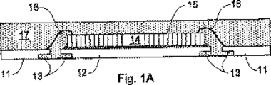
ここに図1Aを参照すると、ダイパドル12及びリード11を含むリードフレームを有する従来のリードフレームパッケージが示され、これは、ダイパドルの端縁とリードとの間に隙間が存在するように配置されるものである。第一のダイ14は、ダイパドル12の第一(“上部”)面上に設置(マウント)され、ダイ取付接着剤15を用いて取り付けられる。ダイ14は、ダイ14のボンドパッドとリード11のボンドサイトとを接続するワイヤボンド16によって、リードフレームと電気的に相互接続される。ダイとワイヤボンドとリードフレームの上部の面の領域は、封入体17によって保護され、封入体17は、さらにダイパドルの端縁とリードとの間の隙間を埋める。リードフレームの第二(“下部”)の面においてリードフレームの端縁と封入体との間に改善された連結を形成すべく、リード及びダイパドルの端縁は、13で示されるように下を切り取られる。特定用途における電気回路に対するパッケージの電気的相互接続は、リードの下部の面を、例えばはんだボール(図示しない)によって例えばマザーボード(図示しない)などのプリント基板と接続することによって形成される。
Referring to FIG. 1A herein, is shown a conventional leadframe package having a leadframe including a
図1Bは、図1Aにおけるような従来のリードフレームを概略的に示し、第一のダイ14に載置された追加のダイ124を有する。追加のダイ124は、接着剤125を用いて第一のダイ14に取り付けられ、それは、ダイ124のボンドパッドをリード11のボンドサイトと接続するワイヤボンド126によってリードフレームと電気的に相互接続される。パッケージは、概略的に図1A中の実施形態に関しては、封入17される。図1Aのような構造と同様のフットプリントを有するこのようなスタックされた(積み重ねられた)構造は、追加の厚みの犠牲においてパッケージ中の半導体デバイスのより高い密度を達成する。
FIG. 1B schematically shows a conventional lead frame as in FIG. 1A, with an additional die 124 mounted on the first die 14. An additional die 124 is attached to the first die 14 using an adhesive 125, which is electrically interconnected with the lead frame by
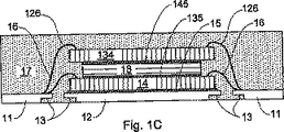
図1Bの実施形態における追加のダイ124は、第一のダイに設置される追加のダイが第一のダイのボンドパッドに接触しないように、第一のダイ14より小さいフットプリントを有する。第一のダイの上により大きな追加のダイを積み重ねることが要望される場合には、例えば図1Cに示されるように、第一のダイと追加のダイとの間にスペーサーが使用され得る。この実施形態において、第一のダイ14は、リードフレームダイパドル12の上に設置され、図1A及び1Bに概略的に示されるようなダイ取付接着剤15を用いて、そこに取り付けられる。例えばシリコンの“ダミー”ダイであり得るスペーサー18は、第一のダイに設置され、接着剤135を用いて取り付けられる。第二のダイ134は、スペーサー18の上に設置され、接着剤145を用いてそこに取り付けられる。第二のダイ134は、該第二のダイ134のボンドパッドをリード11のボンドサイトと接続するワイヤボンド126によって電気的に相互接続される。第一のダイ14は、該ダイ14のボンドパッドをリード11のボンドサイトと接続するワイヤボンド16によってリードフレームと電気的に相互接続される。スペーサー18の厚みは、第二のダイ124の底面とワイヤボンド16のワイヤループとの間での接触を避けるために、接着剤135及び145の厚みとともに、第一及び第二のダイ間に十分なクリアランスを提供するのに十分に大きくされる。パッケージは、一般に図1Aにおける実施形態については封入17される。
The additional die 124 in the embodiment of FIG. 1B has a smaller footprint than the first die 14 so that the additional die placed on the first die does not contact the bond pad of the first die. If it is desired to stack a larger additional die on top of the first die, a spacer may be used between the first die and the additional die, for example as shown in FIG. 1C. In this embodiment, the first die 14 is placed on the leadframe die
図1Dは、ダイをリードフレームの上部の面だけでなく下部の面にも設置することによって、より高いダイ密度が実現されたマルチチップリードパッケージを説明する。リードフレームは、ダイパドル112及びリード111を含み、ダイパドルの端縁とリードとの間には隙間を有する。第一(“上部”)のダイ164は、ダイパドル112の上部の面に載置され、接着剤155を用いてそこに取り付けられる。第二(“下部”)のダイ154は、“センターパッド”チップである。;即ち、それらは、ボンドパッドがダイのアクティブな面の中心線に向かって配されるダイである。第二のダイ154のそれぞれは、リードフレームの下部の面に設置され、ダイのボンドパッドが隙間の中にあるように置かれる。;そして、第二のダイ154のそれぞれは、接着剤の153を用いて、一部がダイパドルの下部の面に取り付けられ、一部がリードの下部の面に取り付けられる。上部のダイ164は、該上部のダイ164のボンドパッドをリード111のボンドサイトと接続するワイヤボンド156によって、電気的に相互接続される。;そして、下部のダイ154は、下部のダイ154のパッドをリード111のボンドサイトと接続する接続ボンド159によって、電気的に相互接続され、任意的に、下部のダイ154のパッドを上部のダイ164のボンドパッドと接続するワイヤボンド158によって電気的に相互接続される。パッケージは、ダイ及びワイヤループを封止するために封入157され、パッケージが用いられることとなる機器(図示されない)に相互接続されるためのリード111の突出部分はそのままとされる。
FIG. 1D illustrates a multichip lead package in which a higher die density is achieved by placing the die on the lower surface as well as the upper surface of the lead frame. The lead frame includes a
図1Eは、図1Dのパッケージに関するリードフレームの平面図を示す。図1Eのリードフレームにおいて、リード111は、中心に位置するダイパドル112の対向する二つの概ね直線状の端縁に隣接させて、ダイパドルの端縁とリードのそれぞれの列との間に隙間を有した状態で、二列に並べて配される。
FIG. 1E shows a top view of the lead frame for the package of FIG. 1D. In the lead frame of FIG. 1E, the
図2A−図2Cは、本発明の一つの実施形態に係るマルチチップパッケージを示す。図2A及び図2Cは、この実施形態に係るリードフレームの平面図を示し、図2Aは、“上部”の側を示し、図2Cは、“下部”の側を示す。;そして、図2Bは、そのような実施形態に係る、全体として202で示すパッケージの、図2A又は2Cにおける2B−2B断面図を示す。リードフレームは、中心に置かれたダイパドル212と周辺に配されたリードとを含む。ダイパドル212は、周辺領域232を含み、リードは、内側のボンドフィンガー部231とランド部211とを含む。多くのそのようなリードフレームは、一般に、銅などの金属のシートに列に並んで形成される。パッケージは、列に並んだリードフレームに形成され、それから、完成した個々のパッケージは、のこぎり切断(ソーイング)又は打ち抜き(パンチング)によって分離(シンギュレート)される。図2A及び図2Cの破線241は、図2Bに241で示されるように、完成したパッケージの端縁を形成するためのシンギュレーションラインを示す。第一(“上部”)のダイ24は、ダイパドル212の上部の面の表面のダイ取付領域に設置され、接着剤25を用いて取り付けられる。上部のダイのフットプリントは、図2Aにおいて網掛けされた領域24によって示される。上部のダイは、ダイのボンドパッドをリードフィンガー231のボンドサイトと接続するワイヤボンド26によって電気的に相互接続される。リードフレームは、下面に、リードのボンドフィンガー部231及びダイパドル212の周辺領域232に形成された段差233,234によって、キャビティが設けられる。下部のダイ224は、キャビティに設置され、ダイパドルの周辺領域及びリードのボンドフィンガー部232,231における段差234,233のダイ取付領域に接着剤225を用いてそれぞれ取り付けられる。下部のダイ224は、センターパッドダイである。;即ち、ボンドパッドは、ダイのアクティブな面の中線の方を向いて位置する。下部のダイ224のそれぞれは、ダイパドル212の端縁236とボンドフィンガー231の端部235との間の隙間237に架かるように置かれ、従って、ダイのボンドパッドは、隙間237の中に位置する。下部のダイのフットプリントは、図2Cにおいて網掛けされた領域214によって示される。下部のダイ224は、ダイのボンドパッドとボンドフィンガーのボンドサイトとの間の隙間237を通過するワイヤボンド226によって電気的に相互接続される。封入体217は、ダイ及びワイヤボンドを覆い保護する。;この実施形態において、リードのランド端部211の下部側の表面の部分251とダイパドル212の下部側の表面の中間部分252とは、封入体によってカバーされず、露出したままとされる。図2Bに示された封入体は、モールド(型成形)される(図3Cと比較)。パッケージが用いられる(第二レベル相互接続)装置(図示しない)の電気回路を有するパッケージの電気的相互接続は、リードのランド端部の露出部分251との接触によって形成され、例えば、例えばマザーボードなどのプリント基板とのはんだボール相互接続によって形成される。ダイパドルの露出部分252は、ダイからの、及び、パッケージの外への熱伝導及び消散に役立てることができる。
2A-2C illustrate a multi-chip package according to one embodiment of the present invention. 2A and 2C are plan views of the lead frame according to this embodiment, FIG. 2A shows the “upper” side, and FIG. 2C shows the “lower” side. 2B shows a 2B-2B cross-sectional view in FIG. 2A or 2C of a package, generally designated 202, according to such an embodiment. The lead frame includes a
本発明に係るリードフレームは、マスキング及びエッチングを行うことによって、銅板などのリードフレーム材料のシートから作製することができる。段差は、例えば、下部側からシートを通して部分的にマスキング及びエッチングを行うことによって形成することができ、ダイパドル及びリードの平面図の形状は、シートを通して全体的にマスキング及びエッチングを行うことによって形成される。段差の深さは、リードフレーム技術の中でよく知られている手段に従って、エッチを制御することによって限定することができる。段差を形成する部分的なエッチは、(他のエッチング工程と同様に、)実際には、図面に示されるような、正確な平面且つ平行又は直角の面を形成することを期待されないであろう。本発明によると、キャビティの深さ、即ち、段差が成形される深さは、下部のダイ及びダイ取付接着剤の厚みに対応するのに十分である必要がある。;そして、キャビティの幅及び長さは、下部のダイのフットプリントに対応するのに十分である必要がある。キャビティのダイ取付面は、ダイを設置し、ダイ取付接着剤を用いてダイを取り付けるのに適当な面を提供するために、十分に平らである必要がある。 The lead frame according to the present invention can be manufactured from a sheet of lead frame material such as a copper plate by performing masking and etching. The step can be formed, for example, by partially masking and etching through the sheet from the bottom side, and the shape of the plan view of the die paddle and lead is formed by performing masking and etching entirely through the sheet. The The depth of the step can be limited by controlling the etch according to means well known in the lead frame art. A partial etch that forms a step (like any other etching step) would not actually be expected to form an exact plane and parallel or perpendicular plane as shown in the drawing. . According to the present invention, the depth of the cavity, i.e. the depth at which the step is formed, needs to be sufficient to accommodate the thickness of the lower die and die attach adhesive. And the width and length of the cavity need to be sufficient to accommodate the bottom die footprint. The die attach surface of the cavity must be sufficiently flat to provide a suitable surface for installing the die and attaching the die using a die attach adhesive.
図2Dは、本発明に従うリードフレームの、拡大され厚み寸法を指し示すべく印が付けられた図2Bの一部分を示す。特に、リードに形成された段差233に設置され且つ接着剤225を用いてそこに取り付けられた第二のダイ224の一部分と、封入体227の一部分とともに、ランド部211の一部分とリードのボンドフィンガー部231とが示される。ダイ224の厚みはTOであり、接着剤225の厚みはTAである。段差の深さは、少なくともダイの厚みの合計TD+A及び接着剤と同じくらい大きい必要があり、一般的には、封入体227は、厚みTEを有する封入体の層でダイの背面を覆うことが好ましい。従って、段差の深さは、好ましくはTD+AとTEとの和に等しい深さを有し得る。ボンドフィンガーの段差がつけられた部分の厚みはTFであり、従って、リードフレームの全厚TOは、少なくともTD+A+TFである必要があり、好ましくは、TD+A+TF+TEであり得る。
FIG. 2D shows a portion of FIG. 2B marked to indicate an enlarged thickness dimension of a lead frame according to the present invention. In particular, a part of the
従って、本発明に従う特定の実施形態における段差に必要とされる深さは、選択された下部のダイの厚み及び下部のダイ取付接着剤の厚みに依存するであろう。様々なダイの厚みは、広範囲に亘って異なるものである。;本発明に適した下部のダイは、比較的薄いかもしれず、半導体ウエハは、裏面研削によって薄くされ得るが、実際の問題として、最小のダイ厚みは、特定のダイのタイプに一部依存し得る。約100マイクロメートル未満の厚みに裏面研削することは、ある半導体タイプに対しては少なくとも現在ありふれたものである。;そして、処理が改良されるにつれて、より一層薄いダイが製造され得る。また、種々のダイ取付接着剤は、ダイ取付に効果的な種々の厚みを有する。一般的に、薄膜接着剤は、より薄いかもしれない。;しかし、段差のダイ取付面がかなり非平面状であるならば、ダイアタッチペーストエポキシなどのペースト接着剤がより適当であり得る。例えば、典型的なコントローラダイは、約80マイクロメートル以下の厚みを有し、ダイ取付接着剤は、約20マイクロメートルの厚みを有し、そのような例では、厚みTD+Aは、約100マイクロメートル以下である。本発明に従うボンドフィンガーの厚みTFは、約100マイクロメートル未満であり、通常、約75マイクロメートル未満であり、好ましくは、約50マイクロメートル未満である。 Accordingly, the depth required for the step in a particular embodiment according to the present invention will depend on the thickness of the selected lower die and the lower die attach adhesive. The thickness of the various dies varies over a wide range. The bottom die suitable for the present invention may be relatively thin and the semiconductor wafer may be thinned by back grinding, but in practice the minimum die thickness depends in part on the particular die type obtain. Back grinding to a thickness of less than about 100 micrometers is at least now common for some semiconductor types. And as processing improves, thinner die can be produced. Also, the various die attach adhesives have various thicknesses that are effective for die attach. In general, thin film adhesives may be thinner. However, paste adhesives such as die attach paste epoxies may be more suitable if the step die attach surface is fairly non-planar. For example, a typical controller die has a thickness of about 80 micrometers or less, a die attach adhesive has a thickness of about 20 micrometers, and in such an example, the thickness T D + A is about 100 micrometers or less. The thickness TF of the bond finger according to the present invention is less than about 100 micrometers, usually less than about 75 micrometers, and preferably less than about 50 micrometers.
本発明に従うリードフレーム(即ち、リードフレームの金属板出発材料の厚み)の全厚TOは、より薄い従来のリードフレームより大きいかもしれない。例えば、選択された下部のダイが約80マイクロメートルの厚みを有し、ダイ取付接着剤が約20マイクロメートルの厚みを有する場合、キャビティの深さは少なくとも約100マイクロメートル(4ミル)である必要があり、ボンドフィンガーが約50マイクロメートル(2ミル)の厚みを要求される場合には、リードフレームの全厚は、少なくとも約150マイクロメートル(6ミル)である必要がある。本発明によると、選択された下部のダイ及びダイアタッチエポキシの厚み、及び、ボンドフィンガーの特定の厚みにより、及び、下部のダイの背面が露出することとなるか封入体の薄い層によって覆われることとなるかにより、リードフレームの厚みは、約300マイクロメートル(12ミル)にもなり得る。下部のダイが封入体の薄い層によって覆われることとなる場合には、厚みTEは、封入の間、下部のダイの表面と型との間で封入体が流れるのを可能とすべく十分に大きいべきである。;厚みTEが最小化可能な範囲は、当該技術で周知の他の要因のうちでも、封入体材料及びダイの表面の領域の流動特性に依存するであろう。一方で、現在は、50マイクロメートルもの薄さのダイも製造可能である。 The total thickness T O of the lead frame according to the invention (ie, the thickness of the lead frame metal plate starting material) may be larger than the thinner conventional lead frame. For example, if the selected lower die has a thickness of about 80 micrometers and the die attach adhesive has a thickness of about 20 micrometers, the cavity depth is at least about 100 micrometers (4 mils). If required and the bond fingers are required to have a thickness of about 50 micrometers (2 mils), the total leadframe thickness should be at least about 150 micrometers (6 mils). According to the present invention, the thickness of the selected lower die and die attach epoxy, and the specific thickness of the bond fingers, and the back of the lower die will be exposed or covered by a thin layer of inclusions Depending on the circumstances, the lead frame thickness can be as much as about 300 micrometers (12 mils). If the lower die is to be covered by a thin layer of inclusion, the thickness TE is sufficient to allow the inclusion to flow between the lower die surface and the mold during encapsulation. Should be great. ; Minimizable range thickness T E is, among other factors well known in the art, will depend on the flow characteristics of the region of the encapsulant material and the die surface. On the other hand, dies as thin as 50 micrometers can now be manufactured.
一例として、本発明に従うパワーアンプパッケージにおいては、上部のダイは、例えばパワーアンプであり得るし、下部のダイは電力制御装置であり得るか、又は、他の機能を有し得る(又は、様々な下部のダイは様々なタイプのものであり得る)。様々な理由により、特に、コントローラのパワーアンプとの相互接続を短縮することによってコントロール機能をより速くすることができるため、パワーアンプダイと同じパッケージの中にコントローラダイを有することが好ましい。一般的に、パワーアンプがかなりの量の熱を発生させるため、本発明に従うそのような構成の利点の1つは、ダイパドルの下部側の面が周囲に曝され、−(例えば、マザーボードなどのプリント基板への取付による)ヒートシンクと接触すること、又は、換気の気流に曝すことによって−、パッケージから放熱を行う効果的な手段を提供することである。 As an example, in a power amplifier package according to the present invention, the upper die may be a power amplifier, for example, and the lower die may be a power controller, or may have other functions (or various The lower die can be of various types). For various reasons, it is preferable to have the controller die in the same package as the power amplifier die, especially because the control function can be made faster by shortening the interconnection of the controller with the power amplifier. In general, one of the advantages of such a configuration according to the present invention is that the lower surface of the die paddle is exposed to the environment since the power amplifier generates a significant amount of heat, such as-(e.g., Motherboard) To provide an effective means of dissipating heat from the package by contact with a heat sink (by attachment to a printed circuit board) or by exposure to a ventilation airflow.
本発明に従うマルチチップパッケージは、ダイパドル及びリードを有し、下部側に形成されたキャビティを有するリードフレームを提供することによって作製される。キャビティは、選択された下方のダイの厚み及びフットプリントに対応する寸法とされる。リードフレームは、サポートに置かれ、下方のダイは、それぞれのキャビティに設置され、接着フィルム又はペーストエポキシなどのダイ取付接着剤を用いて取り付けられる。接着剤は、その後の処理の間、キャビティの中に下方のダイを固定すべく、硬化処理される、又は、部分的に硬化処理され得る。或いは、下方のダイは、バンプ又はボールを介してフリップチップ相互接続によって設置され、それは、例えばはんだ又は金のバンプであり得る。次に、リードフレームは、裏返しにされてサポートに置かれ、第一の上方のダイは、ダイパドルの上部面に設置され、接着フィルム又はペーストエポキシなどの接着剤を用いて取り付けられる。接着剤は、硬化処理されるか又は部分的に硬化処理され得る。そして、任意的に、第二の上方のダイが第一の上方のダイに設置され、接着剤を用いて取り付けられる。積み重ねられたダイ間にスペーサーが必要とされる場合には、スペーサーが第一のダイの上に積み重ねられて、第二のダイがスペーサーに積み重ねられ、スペーサーも第二のダイも接着剤を用いて取り付けられ得る。ワイヤボンド手段を用いて、ワイヤボンド相互接続が適切な順序で形成される。例えば、第一の上方のダイの取付の後に、下方のダイからワイヤボンドを形成し、間隔をおいて配置された第二の上方のダイの取付の前に、第一の上方のダイからワイヤボンドを形成するのが好適であり得る。全てのワイヤボンドが形成されると、ダイ及びワイヤは、封入体材料又は成形化合物を用いて封入され、そして硬化処理される。封入体は、モールドされて、その結果、リードのランドの端部の上部の周縁部が露出した状態のままとされるか、又は、モールドされない。典型的であるが、列に並んだパッケージが形成されると、パッケージは、のこぎり切断又はパンチングによってシンギュレートされ、封入体がモールドされない場合には、のこぎり又はパンチのシンギュレーションは、封入体だけでなくリードフレームを通って切断する。プロセスにおける他の段差は、技術に従って推察されるであろう。;例えば、段差の洗浄は、様々な時点で(例えば、特に、ワイヤボンド工程に先立って、及び、封入に先立って)実行され得る。 A multi-chip package according to the present invention is fabricated by providing a lead frame having a die paddle and leads and having a cavity formed on the lower side. The cavity is dimensioned to correspond to the selected lower die thickness and footprint. The lead frame is placed on the support and the lower die is placed in the respective cavity and attached using a die attach adhesive such as an adhesive film or paste epoxy. The adhesive can be cured or partially cured to secure the lower die in the cavity during subsequent processing. Alternatively, the lower die is placed by flip chip interconnection via bumps or balls, which can be, for example, solder or gold bumps. The lead frame is then turned over and placed on the support, and the first upper die is placed on the top surface of the die paddle and attached using an adhesive such as an adhesive film or paste epoxy. The adhesive can be cured or partially cured. And optionally, a second upper die is placed on the first upper die and attached using an adhesive. If a spacer is required between the stacked dies, the spacer is stacked on top of the first die, the second die is stacked on the spacer, and both the spacer and the second die use adhesive. Can be attached. Wire bond interconnects are formed in the proper order using wire bond means. For example, after attachment of the first upper die, a wire bond is formed from the lower die and the wire from the first upper die is attached before attachment of the spaced second upper die. It may be preferred to form a bond. Once all wire bonds have been formed, the die and wire are encapsulated using an encapsulant material or molding compound and cured. The encapsulant is molded so that the upper peripheral edge of the end of the lead land is left exposed or not molded. Typically, when a side-by-side package is formed, the package is singulated by sawing or punching, and if the enclosure is not molded, saw or punch singulation can only be performed by the enclosure. Cut through the lead frame without. Other steps in the process will be inferred according to the technology. For example, step cleaning may be performed at various times (eg, in particular prior to the wire bond process and prior to encapsulation);
図3Aの断面図において例301として示された実施形態は、図2Bにおけるものと類似している。;図3Aの実施形態において、下部のダイ214の電気的相互接続は、ダイパドルの端部とボンドフィンガーとの間の隙間を通過し、下部のダイ及び上部のダイのそれぞれのダイパッドを接続するワイヤボンド316によって、上部のダイ24に形成される。図3Aにおけるリードフレームのランドの端部311は、図2Bにおけるより大きいことが示され、即ち、(パンチ又はソーシンギュレーションによって形成された)ランドの端部の端縁341が封入体217から横方向に離間して突出する。;より大きなランド端部により、例えば以下の図3Dに示されるように、例えばはんだボールによって、1つのそのようなパッケージと、その上に積み重ねられた第二のパッケージとの間の相互接続が可能となる。
The embodiment shown as example 301 in the cross-sectional view of FIG. 3A is similar to that in FIG. 2B. In the embodiment of FIG. 3A, the electrical interconnection of the lower die 214 passes through the gap between the end of the die paddle and the bond finger and connects the respective die pads of the lower die and the upper die. A
図3Bの断面図において例302として示された実施形態も、図2Bにおけるものと類似している;図3Bの実施形態において、追加の上部のダイ324は、第一の上部のダイ24に積み重ねられ、接着剤325を用いて取り付けられる。第一の上部のダイ24の電気相互接続、及び、追加の上部のダイ324の電気相互接続は、第一の上部のダイ24のボンドパッドをボンドフィンガー231のボンドサイトと接続するワイヤボンド26によって、及び、追加の上部のダイ324のボンドパッドをボンドフィンガー231のボンドサイトと接続するワイヤボンド326によって形成される。図3Aにおけるリードフレームのランドの端部311は、図2Bにおけるより大きいことが示され、即ち、(パンチ又はソーシンギュレーションによって形成された)ランドの端部の端縁341が封入体217から横方向に離間して突出する。;より大きなランド端部により、例えば以下の図3Dに示されるように、1つのそのようなパッケージと、その上に積み重ねられた第二のパッケージとの間の相互接続が可能となる。
The embodiment shown as example 302 in the cross-sectional view of FIG. 3B is also similar to that in FIG. 2B; in the embodiment of FIG. 3B, the additional upper die 324 is stacked on the first
図3Cの断面図において例303として示された実施形態は、図2Bにおけるものと類似している。;図3Cの実施形態において、封入されたパッケージは、封入体327及びリードフレームのリードの端部361を通ってパンチング又はソーイングされることによってシンギュレートされる。また、この実施形態では、下部のダイ24のボンドパッドをボンドフィンガー231のボンドサイトと接続する追加のワイヤボンド相互接続346が、隙間を通過して設けられる。
The embodiment shown as example 303 in the cross-sectional view of FIG. 3C is similar to that in FIG. 2B. In the embodiment of FIG. 3C, the encapsulated package is singulated by being punched or sawed through the encapsulant 327 and the
上述のように、本発明に従う様々なパッケージのいずれも、マルチパッケージモジュールを形成すべく、他のパッケージに積み重ねられ得る(他のパッケージは、本発明に従って形成される場合もそうでない場合もある)。一例として、図3Dには、本発明に従う2つのパッケージ306,307を有するマルチパッケージモジュール304の実施形態を示し、2つのパッケージ306,307は、一方を他方に積み重ね、且つ、下方のパッケージ306のリードフレーム346のランドの端部387の上部面381と、上方のパッケージ307のリードフレーム347のランドの端部377の下部面371との間に配置されたはんだボール316によって相互接続される。本発明に従うマルチパッケージモジュールは、2つより多い積み重ねられたパッケージを有し得る。その少なくとも一つは、本発明に従うリードフレームパッケージである。本発明に従うそのようなマルチパッケージモジュールにおけるパッケージは、同一である必要はない。;上述したように、本発明によると、そのようなマルチパッケージの中のパッケージの少なくとも1つは、本発明に従うリードフレームパッケージである。
As noted above, any of the various packages according to the present invention can be stacked on other packages to form a multi-package module (other packages may or may not be formed according to the present invention). . As an example, FIG. 3D shows an embodiment of a
図3Eは、本発明のさらに他の実施形態を全体として305で示し、その中では、キャビティのダイ取付面にマウントされる下部のパッケージ314のそれぞれが、フリップチップ相互接続によって、即ち、金のバンプ又ははんだバンプであり得る導電性のボール又はバンプ325を介して、ダイの上に設置される。ボール又はバンプ325は、下部のフリップチップダイ314をキャビティのダイ取付面に取り付ける機能をし、且つ、ダイとダイパドルの周辺領域との間、及び、ダイと様々なリードのボンドフィンガー231との間の電気相互接続を提供する。下部のダイ314の取付は、封入体357によって補強される。例えば、図2Bの実施形態におけるように、リードフレームの端縁371は、ソー又はパンチシンギュレーションによって画定され、リードのランドの端部381の表面の一部は、封入体357に覆われず、パッケージが用いられることとなる装置(図示しない)との第二レベル相互接続のために露出した状態のままとされる。
FIG. 3E illustrates yet another embodiment of the present invention, generally designated 305, in which each of the
例えば図3Bを参照して上述したように、本発明によると、追加のダイは、リードフレームの上部の面の上の第一のダイの上に積み重ねられ得る。また、本発明に従って、追加のダイは、リードフレームの下部側のキャビティの中に設置され得る。これらの選択肢の両方ともが図4A−図4Cに図示され、本発明の他の実施形態に係るマルチチップパッケージが図示される。図4A及び図4Cは、この実施形態に係るリードフレームの平面図を示し、図4Aは、“上部”側を示し、図4Cは、“下部”側を示す。;そして、図4Bは、全体として402で示すそのような実施形態に係るパッケージの、図4A又は図4Cにおける4B−4Bを通る断面図を示す。ここで、図2A−図2Cの実施形態におけるように、リードフレームは、中心に置かれたダイパドル212と周辺に配されたリードとを含む。ダイパドル212は、周辺領域232を含み、リードは、内側のボンドフィンガー部231とランド部211とを含む。そのようなリードフレームの多くは、銅などの金属のシートに列に並んで形成される。パッケージは、リードフレームの列の上に形成され、それから、完成した個々のパッケージは、ソー又はパンチによって分離(シンギュレート)される。図4A及び図4Cの破線241は、図4Bにおいて241で示されるように、完成したパッケージの端縁を形成するためのシンギュレーション線を示す。第一の“上方”のダイ24は、ダイパドル212の上部の側の面のダイ取付領域に設置され、接着剤25を用いて取り付けられる。第一の上方のダイフットプリントは、図2Aにおける網掛けされた領域24によって示される。第二の上方のダイ424は、第一の上部のダイ24に設置され、接着剤425を用いて取り付けられる。第一の上方のダイ24は、ダイのボンドパッドをリードフィンガー231のボンドサイトと接続するワイヤボンド26によって電気的に相互接続され、第二の上方のダイ424は、ダイのボンドパッドをリードフィンガー231のボンドサイトと接続するワイヤボンド426によって電気的に相互接続される。
For example, as described above with reference to FIG. 3B, according to the present invention, additional dies may be stacked on the first die on the top surface of the lead frame. Also, according to the present invention, additional dies can be placed in the lower cavity of the lead frame. Both of these options are illustrated in FIGS. 4A-4C, illustrating a multi-chip package according to another embodiment of the present invention. 4A and 4C are plan views of the lead frame according to this embodiment, FIG. 4A shows the “upper” side, and FIG. 4C shows the “lower” side. And FIG. 4B shows a cross-sectional view of such a package, generally designated 402, through 4B-4B in FIG. 4A or 4C. Here, as in the embodiment of FIGS. 2A-2C, the lead frame includes a
ここでも、図2A−図2Cの実施形態におけるように、ダイパドル212の周辺領域232の中、及び、リードのボンドフィンガー部231の中に形成された段差233,234によって、下部側のダイのリードフレームの中にキャビティが形成される。下部のダイ214及び追加の下部のダイ424は、キャビティの中に設置され、ダイ取付接着剤225を用いて、それぞれ、ダイパドルの周辺領域及びリードのボンドフィンガー部232,231の段差234,233のダイ取付領域に取り付けられる。下部のダイ214及び424は、センターパッドダイである。;即ち、ボンドパッドは、ダイのアクティブな面の中線の方に位置する。下部のダイ214,424のそれぞれは、ダイパドル212の端縁236とボンドフィンガー231の端部235との間の隙間237を跨ぐように、且つ、ダイのボンドパッドが隙間237の中にあるように置かれる。下部のダイのフットプリントは、図4Cにおける網掛けされた領域214及び414で示される。下部のダイ214及び424は、ダイのボンドパッドとボンドフィンガーのボンドサイトとの間の隙間237を通過するワイヤボンド226によって電気的に相互接続される。封入体427は、ダイ及びワイヤボンドを覆い保護する。;この実施形態では、リードのランド端部211の下部側の表面の部分251と、ダイパドル212の下部側の表面の中間部252とが、封入体に覆われず、露出した状態のままとされる。図4Bに示す封入体は、モールドされる(図3Cと比較)。パッケージと該パッケージが用いられる装置(図示しない)の電気回路との電気相互接続(第二レベル相互接続)は、リードのランド端部の露出部分251との接触を介して形成され、例えば、例えばマザーボードなどのプリント基板とのはんだボール相互接続によって形成される。ダイパドルの露出部分252は、ダイからの、及び、パッケージの外への熱伝導及び消散に役立てることができる。
Again, as in the embodiment of FIGS. 2A-2C, the lower die leads are formed by steps 233,234 formed in the
図2Aと図2C、及び、図4Aと図4Cの実施形態において、キャビティは連続しており、これらの各実施形態の中で、下部のダイのそれぞれは、同じ連続的なダイキャビティの異なる領域に設置されると考えられ得る。即ち、ダイパドルの段差は、ダイパドルの周辺領域の周りに連続的に延びる。;そして、(隙間を越えて)対向する段差は、全てのリードフィンガーに形成される。他のバリエーションが考えられる。;各キャビティは、その中に設置されることとなる選択されたダイのフットプリント(長さ及び幅)を収容するのに十分に大きい必要がある。例えば図2A,2Cにおけるような、ダイパドルの対向する端縁に沿って隙間を越えて配置される2つの下部のダイを有する実施形態では、ダイパドルの周辺領域及びリードの段差は、他の2つの端縁まで延びる必要はなく、リードフレームの角部の中まで延びる必要もない。 In the embodiments of FIGS. 2A and 2C and FIGS. 4A and 4C, the cavities are continuous, and in each of these embodiments, each of the lower dies is a different region of the same continuous die cavity. It can be considered that it is installed in. That is, the step of the die paddle extends continuously around the peripheral area of the die paddle. And an opposing step (over the gap) is formed on every lead finger. Other variations are possible. Each cavity needs to be large enough to accommodate the footprint (length and width) of the selected die that will be placed in it; For example, FIG. 2A, such as in 2C, in an embodiment having two lower dies along opposite edges of the die paddle is positioned beyond the gap, the peripheral area, and a lead of the die paddle step is the other It does not need to extend to the two edges, nor does it need to extend into the corners of the lead frame.
ここに参照された全ての特許及び特許公報は、参照することによって組み込まれる。 All patents and patent publications referenced herein are incorporated by reference.
他の実施形態も本発明の範囲内のものである。 Other embodiments are also within the scope of the present invention.
[関連出願への相互参照]
本願は、“マルチチップリードフレームパッケージ”というタイトルの2004年10月18日に出願された米国仮出願第60/619,847号に基づく優先権を主張する。
[Cross-reference to related applications]
This application claims priority from US Provisional Application No. 60 / 619,847, filed Oct. 18, 2004, entitled “Multi-Chip Leadframe Package”.
Claims (5)
前記リードフレームは、ダイパドル及びリードを備え、各前記リードは、外側のランド部及び内側のボンドフィンガー部を備え、前記ダイパドルは、周辺領域及び端縁を有し、前記ダイパドルの端縁と前記リードのボンドフィンガー部の内側端縁との間には、隙間があり、前記ダイパドルの第一面の表面は、第一面ダイ取付領域を含み、前記リードフレームの第二面に、少なくとも一つのキャビティをさらに備え、前記キャビティは、所定の深さを有するとともに、前記隙間の両側に延びる少なくとも一つのダイ設置面を有し、このダイ設置面は、選択された前記第二面のダイのフットプリントに対応して寸法設定され、前記所定の深さは、選択された前記第二面のダイの厚みと選択された前記第二面のダイの設置手段の厚みとの和以上に寸法設定され、
前記第一のダイは、前記第一面ダイ取付領域に取り付けられ、前記第二のダイは、前記キャビティのダイ設置表面に取り付けられるとともに、前記第二のダイのアクティブな表面がキャビティのダイ設置表面の方を向くように方向付けされ、
前記第二のダイは、ワイヤボンドによって前記リードフレームと電気的に相互接続され、前記第二のダイのダイパッドが前記隙間の下にあり、前記ワイヤボンドのワイヤが前記隙間を通過し、該ワイヤの一端が前記第2のダイのダイパッドに接続される、マルチチップリードフレーム半導体パッケージ。A multi-chip lead frame semiconductor package comprising a lead frame having a first surface and a second surface, and first and second dies,
The lead frame includes a die paddle and leads, each said lead is provided with an outer land portion and an inner bond finger portion, the die paddle has a peripheral region and edges, said end edge of said die paddle lead between the inner edge of the bond finger portion of, there is a gap, the surface of the first side of the die paddle includes a first surface die attach region, the second surface of the lead frame, at least one cavity further wherein the cavity and having a predetermined depth, having at least one die mounting surface extends on either side of the gap, the die mounting surface is selected the second surface of the die footprint in response to the dimensioning, the predetermined depth is dimension than the sum of the thickness of the mounting means of the second surface of the die and the selected thickness of the die of the second surface which is selected It is set,
Said first die, said mounting et is on the first surface die attach region, wherein the second die, along with attached to the die installation surface of the cavity, the second active surface of the cavity die of the die Oriented to face the installation surface,
Said second die, said electrically to the lead frame interconnected by wire bonds, there die pad of said second die below the gap, the wire of the wire bonds pass through the gap, the wire the end Ru is connected to the die pad of the second die, multi-chip leadframe semiconductor package.
Applications Claiming Priority (3)
| Application Number | Priority Date | Filing Date | Title |
|---|---|---|---|
| US61984704P | 2004-10-18 | 2004-10-18 | |
| US60/619,847 | 2004-10-18 | ||
| PCT/US2005/037258 WO2006044804A2 (en) | 2004-10-18 | 2005-10-17 | Multi chip leadframe package |
Publications (3)
| Publication Number | Publication Date |
|---|---|
| JP2008517482A JP2008517482A (en) | 2008-05-22 |
| JP2008517482A5 JP2008517482A5 (en) | 2008-11-27 |
| JP5011115B2 true JP5011115B2 (en) | 2012-08-29 |
Family
ID=36203633
Family Applications (1)
| Application Number | Title | Priority Date | Filing Date |
|---|---|---|---|
| JP2007537948A Active JP5011115B2 (en) | 2004-10-18 | 2005-10-17 | Multi-chip lead frame semiconductor package |
Country Status (5)
| Country | Link |
|---|---|
| US (2) | US7208821B2 (en) |
| JP (1) | JP5011115B2 (en) |
| KR (1) | KR101037246B1 (en) |
| TW (1) | TWI404184B (en) |
| WO (1) | WO2006044804A2 (en) |
Families Citing this family (50)
| Publication number | Priority date | Publication date | Assignee | Title |
|---|---|---|---|---|
| US7745918B1 (en) | 2004-11-24 | 2010-06-29 | Amkor Technology, Inc. | Package in package (PiP) |
| US20070108635A1 (en) * | 2005-04-28 | 2007-05-17 | Stats Chippac Ltd. | Integrated circuit package system |
| US20070130759A1 (en) * | 2005-06-15 | 2007-06-14 | Gem Services, Inc. | Semiconductor device package leadframe formed from multiple metal layers |
| US8803299B2 (en) * | 2006-02-27 | 2014-08-12 | Stats Chippac Ltd. | Stacked integrated circuit package system |
| US7961470B2 (en) * | 2006-07-19 | 2011-06-14 | Infineon Technologies Ag | Power amplifier |
| US20080054429A1 (en) * | 2006-08-25 | 2008-03-06 | Bolken Todd O | Spacers for separating components of semiconductor device assemblies, semiconductor device assemblies and systems including spacers and methods of making spacers |
| KR100809701B1 (en) * | 2006-09-05 | 2008-03-06 | 삼성전자주식회사 | Multi chip package having spacer for blocking inter-chip heat transfer |
| US7271485B1 (en) | 2006-09-11 | 2007-09-18 | Agere Systems Inc. | Systems and methods for distributing I/O in a semiconductor device |
| US20080079149A1 (en) * | 2006-09-28 | 2008-04-03 | Harry Hedler | Circuit board arrangement and method for producing a circuit board arrangement |
| JP4860442B2 (en) * | 2006-11-20 | 2012-01-25 | ローム株式会社 | Semiconductor device |
| US20080157307A1 (en) * | 2006-12-28 | 2008-07-03 | Semiconductor Manufacturing International (Shanghai) Corporation | Lead frame |
| US20080180921A1 (en) * | 2007-01-31 | 2008-07-31 | Cyntec Co., Ltd. | Electronic package structure |
| US20080179722A1 (en) * | 2007-01-31 | 2008-07-31 | Cyntec Co., Ltd. | Electronic package structure |
| TW200921885A (en) * | 2007-11-06 | 2009-05-16 | Powertech Technology Inc | Package on package structure |
| US8643157B2 (en) * | 2007-06-21 | 2014-02-04 | Stats Chippac Ltd. | Integrated circuit package system having perimeter paddle |
| US7919848B2 (en) * | 2007-08-03 | 2011-04-05 | Stats Chippac Ltd. | Integrated circuit package system with multiple devices |
| CN100530636C (en) * | 2007-11-09 | 2009-08-19 | 中国科学院上海微系统与信息技术研究所 | Three-dimensional multiple chips packaging module and preparation method |
| US7692311B2 (en) * | 2007-11-21 | 2010-04-06 | Powertech Technology Inc. | POP (package-on-package) device encapsulating soldered joints between external leads |
| US8618653B2 (en) * | 2008-01-30 | 2013-12-31 | Stats Chippac Ltd. | Integrated circuit package system with wafer scale heat slug |
| US8664038B2 (en) * | 2008-12-04 | 2014-03-04 | Stats Chippac Ltd. | Integrated circuit packaging system with stacked paddle and method of manufacture thereof |
| US8034662B2 (en) * | 2009-03-18 | 2011-10-11 | Advanced Micro Devices, Inc. | Thermal interface material with support structure |
| US20100252918A1 (en) * | 2009-04-06 | 2010-10-07 | Jiang Hunt H | Multi-die package with improved heat dissipation |
| US7994615B2 (en) * | 2009-08-28 | 2011-08-09 | International Rectifier Corporation | Direct contact leadless package for high current devices |
| US8093695B2 (en) | 2009-09-04 | 2012-01-10 | International Rectifier Corporation | Direct contact leadless flip chip package for high current devices |
| KR101119473B1 (en) * | 2009-10-07 | 2012-03-16 | 이성규 | Semiconductor package and method for manufacturing the same |
| US8435837B2 (en) * | 2009-12-15 | 2013-05-07 | Silicon Storage Technology, Inc. | Panel based lead frame packaging method and device |
| US8207015B2 (en) * | 2010-04-30 | 2012-06-26 | Stats Chippac Ltd. | Integrated circuit packaging system with package-on-package and method of manufacture thereof |
| US20120193772A1 (en) * | 2011-01-28 | 2012-08-02 | Hunt Hang Jiang | Stacked die packages with flip-chip and wire bonding dies |
| US9524957B2 (en) | 2011-08-17 | 2016-12-20 | Intersil Americas LLC | Back-to-back stacked dies |
| KR101354894B1 (en) * | 2011-10-27 | 2014-01-23 | 삼성전기주식회사 | Semiconductor package and method for manufacturing the same and semiconductor package module having the same |
| JP2013149779A (en) * | 2012-01-19 | 2013-08-01 | Semiconductor Components Industries Llc | Semiconductor device |
| JP5620437B2 (en) * | 2012-05-18 | 2014-11-05 | ラピスセミコンダクタ株式会社 | Semiconductor device |
| US8759956B2 (en) * | 2012-07-05 | 2014-06-24 | Infineon Technologies Ag | Chip package and method of manufacturing the same |
| JP2014203861A (en) * | 2013-04-02 | 2014-10-27 | 三菱電機株式会社 | Semiconductor device and semiconductor module |
| KR101538543B1 (en) * | 2013-08-13 | 2015-07-22 | 앰코 테크놀로지 코리아 주식회사 | Semiconductor Device and Fabricating Method Thereof |
| TWI550823B (en) * | 2014-04-10 | 2016-09-21 | 南茂科技股份有限公司 | Chip package structure |
| JP2017147272A (en) * | 2016-02-15 | 2017-08-24 | ローム株式会社 | Semiconductor device and manufacturing method thereof, and lead frame intermediate body used to manufacture semiconductor device |
| US11211305B2 (en) | 2016-04-01 | 2021-12-28 | Texas Instruments Incorporated | Apparatus and method to support thermal management of semiconductor-based components |
| US10861796B2 (en) | 2016-05-10 | 2020-12-08 | Texas Instruments Incorporated | Floating die package |
| EP3261115A1 (en) | 2016-06-23 | 2017-12-27 | Nxp B.V. | Chip scale semiconductor package and method of manufacturing the same |
| US9929110B1 (en) | 2016-12-30 | 2018-03-27 | Texas Instruments Incorporated | Integrated circuit wave device and method |
| US10074639B2 (en) | 2016-12-30 | 2018-09-11 | Texas Instruments Incorporated | Isolator integrated circuits with package structure cavity and fabrication methods |
| US10411150B2 (en) | 2016-12-30 | 2019-09-10 | Texas Instruments Incorporated | Optical isolation systems and circuits and photon detectors with extended lateral P-N junctions |
| US10121847B2 (en) | 2017-03-17 | 2018-11-06 | Texas Instruments Incorporated | Galvanic isolation device |
| US10600769B2 (en) * | 2017-09-01 | 2020-03-24 | Airoha Technology Group | Electronic component |
| US20190287881A1 (en) | 2018-03-19 | 2019-09-19 | Stmicroelectronics S.R.L. | Semiconductor package with die stacked on surface mounted devices |
| US10593612B2 (en) * | 2018-03-19 | 2020-03-17 | Stmicroelectronics S.R.L. | SMDs integration on QFN by 3D stacked solution |
| US11177301B2 (en) * | 2018-11-19 | 2021-11-16 | UTAC Headquarters Pte. Ltd. | Reliable semiconductor packages |
| US11817423B2 (en) * | 2019-07-29 | 2023-11-14 | Intel Corporation | Double-sided substrate with cavities for direct die-to-die interconnect |
| TWI781863B (en) * | 2021-12-30 | 2022-10-21 | 宏齊科技股份有限公司 | Planar type multi-chip device |
Family Cites Families (18)
| Publication number | Priority date | Publication date | Assignee | Title |
|---|---|---|---|---|
| DE3531886A1 (en) * | 1985-09-06 | 1987-03-19 | Stankiewicz Alois Dr Gmbh | CAVES |
| JP2902918B2 (en) * | 1993-11-25 | 1999-06-07 | 三洋電機株式会社 | Surface mount type semiconductor device |
| JP3638750B2 (en) * | 1997-03-25 | 2005-04-13 | 株式会社ルネサステクノロジ | Semiconductor device |
| JP3670853B2 (en) * | 1998-07-30 | 2005-07-13 | 三洋電機株式会社 | Semiconductor device |
| US6281568B1 (en) | 1998-10-21 | 2001-08-28 | Amkor Technology, Inc. | Plastic integrated circuit device package and leadframe having partially undercut leads and die pad |
| US6261865B1 (en) * | 1998-10-06 | 2001-07-17 | Micron Technology, Inc. | Multi chip semiconductor package and method of construction |
| JP3730469B2 (en) * | 2000-01-21 | 2006-01-05 | 新電元工業株式会社 | Resin-sealed semiconductor device and manufacturing method thereof |
| KR100559664B1 (en) * | 2000-03-25 | 2006-03-10 | 앰코 테크놀로지 코리아 주식회사 | Semiconductor package |
| JP3442721B2 (en) * | 2000-05-24 | 2003-09-02 | 沖電気工業株式会社 | Semiconductor device |
| JP4574868B2 (en) | 2001-01-12 | 2010-11-04 | ローム株式会社 | Semiconductor device |
| JP3879410B2 (en) | 2001-02-06 | 2007-02-14 | 凸版印刷株式会社 | Lead frame manufacturing method |
| US6608375B2 (en) * | 2001-04-06 | 2003-08-19 | Oki Electric Industry Co., Ltd. | Semiconductor apparatus with decoupling capacitor |
| DE10142117A1 (en) * | 2001-08-30 | 2003-03-27 | Infineon Technologies Ag | Electronic component with at least two stacked semiconductor chips and method for its production |
| TWI268581B (en) * | 2002-01-25 | 2006-12-11 | Advanced Semiconductor Eng | Stack type flip-chip package including a substrate board, a first chip, a second chip, multiple conductive wire, an underfill, and a packaging material |
| KR100460062B1 (en) * | 2002-04-23 | 2004-12-04 | 주식회사 하이닉스반도체 | Multi chip package and manufacturing method thereof |
| JP3550391B2 (en) * | 2002-05-15 | 2004-08-04 | 沖電気工業株式会社 | Semiconductor device and manufacturing method thereof |
| TW548810B (en) * | 2002-05-31 | 2003-08-21 | Gigno Technology Co Ltd | Multi-chip package |
| US7005325B2 (en) * | 2004-02-05 | 2006-02-28 | St Assembly Test Services Ltd. | Semiconductor package with passive device integration |
-
2005
- 2005-10-17 KR KR1020077007844A patent/KR101037246B1/en active IP Right Grant
- 2005-10-17 WO PCT/US2005/037258 patent/WO2006044804A2/en active Application Filing
- 2005-10-17 US US11/252,193 patent/US7208821B2/en not_active Expired - Fee Related
- 2005-10-17 JP JP2007537948A patent/JP5011115B2/en active Active
- 2005-10-18 TW TW094136371A patent/TWI404184B/en active
-
2007
- 2007-03-14 US US11/686,010 patent/US7436048B2/en active Active
Also Published As
| Publication number | Publication date |
|---|---|
| JP2008517482A (en) | 2008-05-22 |
| WO2006044804A3 (en) | 2007-04-19 |
| KR20070095865A (en) | 2007-10-01 |
| US7436048B2 (en) | 2008-10-14 |
| US20060081967A1 (en) | 2006-04-20 |
| KR101037246B1 (en) | 2011-05-26 |
| WO2006044804A2 (en) | 2006-04-27 |
| TW200629516A (en) | 2006-08-16 |
| TWI404184B (en) | 2013-08-01 |
| US7208821B2 (en) | 2007-04-24 |
| US20070152308A1 (en) | 2007-07-05 |
Similar Documents
| Publication | Publication Date | Title |
|---|---|---|
| JP5011115B2 (en) | Multi-chip lead frame semiconductor package | |
| US6909168B2 (en) | Resin encapsulation semiconductor device utilizing grooved leads and die pad | |
| KR100477020B1 (en) | Multi chip package | |
| KR101160694B1 (en) | Manufacturing Method of Semiconductor Device | |
| JP5227501B2 (en) | Stack die package and method of manufacturing the same | |
| US6982488B2 (en) | Semiconductor package and method for fabricating the same | |
| US6873041B1 (en) | Power semiconductor package with strap | |
| JP3420153B2 (en) | Semiconductor device and manufacturing method thereof | |
| US6767767B2 (en) | Method of manufacturing a semiconductor device in which a block molding package utilizes air vents in a substrate | |
| KR100716871B1 (en) | Carrier frame for semiconductor package and semiconductor package using it and its manufacturing method | |
| JP4547279B2 (en) | Manufacturing method of semiconductor device | |
| TWI453838B (en) | No lead package with heat spreader | |
| US6853059B1 (en) | Semiconductor package having improved adhesiveness and ground bonding | |
| US20090045497A1 (en) | Semiconductor device and method of manufacturing the same | |
| JP4068336B2 (en) | Semiconductor device | |
| US20100193922A1 (en) | Semiconductor chip package | |
| TWI430425B (en) | Integrated circuit package system employing bump technology | |
| JP4494240B2 (en) | Resin-sealed semiconductor device | |
| US7564123B1 (en) | Semiconductor package with fastened leads | |
| US6869824B2 (en) | Fabrication method of window-type ball grid array semiconductor package | |
| TWI478252B (en) | A semiconductor package of a flipped mosfet and its manufacturing method | |
| KR100370480B1 (en) | Lead frame for semiconductor package | |
| KR100308393B1 (en) | Semiconductor Package and Manufacturing Method | |
| JP4453009B2 (en) | Semiconductor device and manufacturing method thereof | |
| JP3918748B2 (en) | Semiconductor device |
Legal Events
| Date | Code | Title | Description |
|---|---|---|---|
| A521 | Request for written amendment filed |
Free format text: JAPANESE INTERMEDIATE CODE: A523 Effective date: 20081010 |
|
| A621 | Written request for application examination |
Free format text: JAPANESE INTERMEDIATE CODE: A621 Effective date: 20081010 |
|
| A977 | Report on retrieval |
Free format text: JAPANESE INTERMEDIATE CODE: A971007 Effective date: 20090205 |
|
| RD02 | Notification of acceptance of power of attorney |
Free format text: JAPANESE INTERMEDIATE CODE: A7422 Effective date: 20100810 |
|
| RD04 | Notification of resignation of power of attorney |
Free format text: JAPANESE INTERMEDIATE CODE: A7424 Effective date: 20100823 |
|
| A521 | Request for written amendment filed |
Free format text: JAPANESE INTERMEDIATE CODE: A821 Effective date: 20100810 |
|
| RD04 | Notification of resignation of power of attorney |
Free format text: JAPANESE INTERMEDIATE CODE: A7424 Effective date: 20100823 |
|
| A131 | Notification of reasons for refusal |
Free format text: JAPANESE INTERMEDIATE CODE: A131 Effective date: 20110201 |
|
| A521 | Request for written amendment filed |
Free format text: JAPANESE INTERMEDIATE CODE: A523 Effective date: 20110427 |
|
| A131 | Notification of reasons for refusal |
Free format text: JAPANESE INTERMEDIATE CODE: A131 Effective date: 20110524 |
|
| A521 | Request for written amendment filed |
Free format text: JAPANESE INTERMEDIATE CODE: A523 Effective date: 20110823 |
|
| TRDD | Decision of grant or rejection written | ||
| A01 | Written decision to grant a patent or to grant a registration (utility model) |
Free format text: JAPANESE INTERMEDIATE CODE: A01 Effective date: 20120508 |
|
| A01 | Written decision to grant a patent or to grant a registration (utility model) |
Free format text: JAPANESE INTERMEDIATE CODE: A01 |
|
| A61 | First payment of annual fees (during grant procedure) |
Free format text: JAPANESE INTERMEDIATE CODE: A61 Effective date: 20120604 |
|
| R150 | Certificate of patent or registration of utility model |
Ref document number: 5011115 Country of ref document: JP Free format text: JAPANESE INTERMEDIATE CODE: R150 Free format text: JAPANESE INTERMEDIATE CODE: R150 |
|
| FPAY | Renewal fee payment (event date is renewal date of database) |
Free format text: PAYMENT UNTIL: 20150608 Year of fee payment: 3 |
|
| R250 | Receipt of annual fees |
Free format text: JAPANESE INTERMEDIATE CODE: R250 |
|
| R250 | Receipt of annual fees |
Free format text: JAPANESE INTERMEDIATE CODE: R250 |
|
| R250 | Receipt of annual fees |
Free format text: JAPANESE INTERMEDIATE CODE: R250 |
|
| R250 | Receipt of annual fees |
Free format text: JAPANESE INTERMEDIATE CODE: R250 |
|
| R250 | Receipt of annual fees |
Free format text: JAPANESE INTERMEDIATE CODE: R250 |
|
| R250 | Receipt of annual fees |
Free format text: JAPANESE INTERMEDIATE CODE: R250 |
|
| R250 | Receipt of annual fees |
Free format text: JAPANESE INTERMEDIATE CODE: R250 |
|
| R250 | Receipt of annual fees |
Free format text: JAPANESE INTERMEDIATE CODE: R250 |
|
| R250 | Receipt of annual fees |
Free format text: JAPANESE INTERMEDIATE CODE: R250 |