JP5010660B2 - Semiconductor device and manufacturing method thereof - Google Patents
Semiconductor device and manufacturing method thereof Download PDFInfo
- Publication number
- JP5010660B2 JP5010660B2 JP2009220903A JP2009220903A JP5010660B2 JP 5010660 B2 JP5010660 B2 JP 5010660B2 JP 2009220903 A JP2009220903 A JP 2009220903A JP 2009220903 A JP2009220903 A JP 2009220903A JP 5010660 B2 JP5010660 B2 JP 5010660B2
- Authority
- JP
- Japan
- Prior art keywords
- trench
- film
- layer
- region
- substrate
- Prior art date
- Legal status (The legal status is an assumption and is not a legal conclusion. Google has not performed a legal analysis and makes no representation as to the accuracy of the status listed.)
- Active
Links
- 239000004065 semiconductor Substances 0.000 title claims description 135
- 238000004519 manufacturing process Methods 0.000 title claims description 31
- 239000000758 substrate Substances 0.000 claims description 126
- 238000000034 method Methods 0.000 claims description 94
- 238000009792 diffusion process Methods 0.000 claims description 61
- 230000015572 biosynthetic process Effects 0.000 claims description 53
- 239000012535 impurity Substances 0.000 claims description 48
- 238000002955 isolation Methods 0.000 claims description 28
- 230000003647 oxidation Effects 0.000 claims description 26
- 238000007254 oxidation reaction Methods 0.000 claims description 26
- 238000000059 patterning Methods 0.000 claims description 17
- 238000005530 etching Methods 0.000 claims description 13
- XUIMIQQOPSSXEZ-UHFFFAOYSA-N Silicon Chemical compound [Si] XUIMIQQOPSSXEZ-UHFFFAOYSA-N 0.000 description 29
- 229910052710 silicon Inorganic materials 0.000 description 29
- 239000010703 silicon Substances 0.000 description 29
- 238000001020 plasma etching Methods 0.000 description 21
- BOTDANWDWHJENH-UHFFFAOYSA-N Tetraethyl orthosilicate Chemical compound CCO[Si](OCC)(OCC)OCC BOTDANWDWHJENH-UHFFFAOYSA-N 0.000 description 20
- 230000015556 catabolic process Effects 0.000 description 20
- 238000001459 lithography Methods 0.000 description 15
- 238000004380 ashing Methods 0.000 description 12
- 238000005468 ion implantation Methods 0.000 description 12
- 239000000463 material Substances 0.000 description 12
- 230000000052 comparative effect Effects 0.000 description 10
- 238000004518 low pressure chemical vapour deposition Methods 0.000 description 7
- VYPSYNLAJGMNEJ-UHFFFAOYSA-N Silicium dioxide Chemical compound O=[Si]=O VYPSYNLAJGMNEJ-UHFFFAOYSA-N 0.000 description 6
- 238000010586 diagram Methods 0.000 description 6
- 229910052814 silicon oxide Inorganic materials 0.000 description 6
- 239000004020 conductor Substances 0.000 description 5
- NBIIXXVUZAFLBC-UHFFFAOYSA-N Phosphoric acid Chemical compound OP(O)(O)=O NBIIXXVUZAFLBC-UHFFFAOYSA-N 0.000 description 4
- 238000005229 chemical vapour deposition Methods 0.000 description 4
- LIVNPJMFVYWSIS-UHFFFAOYSA-N silicon monoxide Chemical compound [Si-]#[O+] LIVNPJMFVYWSIS-UHFFFAOYSA-N 0.000 description 4
- 229910000147 aluminium phosphate Inorganic materials 0.000 description 2
- 230000000694 effects Effects 0.000 description 2
- 238000005259 measurement Methods 0.000 description 2
- 230000001590 oxidative effect Effects 0.000 description 2
- 230000001681 protective effect Effects 0.000 description 2
- 238000001039 wet etching Methods 0.000 description 2
- JBRZTFJDHDCESZ-UHFFFAOYSA-N AsGa Chemical compound [As]#[Ga] JBRZTFJDHDCESZ-UHFFFAOYSA-N 0.000 description 1
- ZOXJGFHDIHLPTG-UHFFFAOYSA-N Boron Chemical compound [B] ZOXJGFHDIHLPTG-UHFFFAOYSA-N 0.000 description 1
- 229910001218 Gallium arsenide Inorganic materials 0.000 description 1
- 230000003213 activating effect Effects 0.000 description 1
- 229910052796 boron Inorganic materials 0.000 description 1
- 230000003247 decreasing effect Effects 0.000 description 1
- 230000002093 peripheral effect Effects 0.000 description 1
- 238000005498 polishing Methods 0.000 description 1
- 229910021420 polycrystalline silicon Inorganic materials 0.000 description 1
- 229920005591 polysilicon Polymers 0.000 description 1
- 230000002040 relaxant effect Effects 0.000 description 1
- 238000000926 separation method Methods 0.000 description 1
- 239000000126 substance Substances 0.000 description 1
Images


Classifications
-
- H—ELECTRICITY
- H01—ELECTRIC ELEMENTS
- H01L—SEMICONDUCTOR DEVICES NOT COVERED BY CLASS H10
- H01L29/00—Semiconductor devices adapted for rectifying, amplifying, oscillating or switching, or capacitors or resistors with at least one potential-jump barrier or surface barrier, e.g. PN junction depletion layer or carrier concentration layer; Details of semiconductor bodies or of electrodes thereof ; Multistep manufacturing processes therefor
- H01L29/66—Types of semiconductor device ; Multistep manufacturing processes therefor
- H01L29/68—Types of semiconductor device ; Multistep manufacturing processes therefor controllable by only the electric current supplied, or only the electric potential applied, to an electrode which does not carry the current to be rectified, amplified or switched
- H01L29/70—Bipolar devices
- H01L29/72—Transistor-type devices, i.e. able to continuously respond to applied control signals
- H01L29/73—Bipolar junction transistors
- H01L29/732—Vertical transistors
- H01L29/7322—Vertical transistors having emitter-base and base-collector junctions leaving at the same surface of the body, e.g. planar transistor
-
- H—ELECTRICITY
- H01—ELECTRIC ELEMENTS
- H01L—SEMICONDUCTOR DEVICES NOT COVERED BY CLASS H10
- H01L21/00—Processes or apparatus adapted for the manufacture or treatment of semiconductor or solid state devices or of parts thereof
- H01L21/70—Manufacture or treatment of devices consisting of a plurality of solid state components formed in or on a common substrate or of parts thereof; Manufacture of integrated circuit devices or of parts thereof
- H01L21/71—Manufacture of specific parts of devices defined in group H01L21/70
- H01L21/76—Making of isolation regions between components
- H01L21/762—Dielectric regions, e.g. EPIC dielectric isolation, LOCOS; Trench refilling techniques, SOI technology, use of channel stoppers
- H01L21/76224—Dielectric regions, e.g. EPIC dielectric isolation, LOCOS; Trench refilling techniques, SOI technology, use of channel stoppers using trench refilling with dielectric materials
-
- H—ELECTRICITY
- H01—ELECTRIC ELEMENTS
- H01L—SEMICONDUCTOR DEVICES NOT COVERED BY CLASS H10
- H01L29/00—Semiconductor devices adapted for rectifying, amplifying, oscillating or switching, or capacitors or resistors with at least one potential-jump barrier or surface barrier, e.g. PN junction depletion layer or carrier concentration layer; Details of semiconductor bodies or of electrodes thereof ; Multistep manufacturing processes therefor
- H01L29/02—Semiconductor bodies ; Multistep manufacturing processes therefor
- H01L29/06—Semiconductor bodies ; Multistep manufacturing processes therefor characterised by their shape; characterised by the shapes, relative sizes, or dispositions of the semiconductor regions ; characterised by the concentration or distribution of impurities within semiconductor regions
- H01L29/10—Semiconductor bodies ; Multistep manufacturing processes therefor characterised by their shape; characterised by the shapes, relative sizes, or dispositions of the semiconductor regions ; characterised by the concentration or distribution of impurities within semiconductor regions with semiconductor regions connected to an electrode not carrying current to be rectified, amplified or switched and such electrode being part of a semiconductor device which comprises three or more electrodes
- H01L29/107—Substrate region of field-effect devices
- H01L29/1075—Substrate region of field-effect devices of field-effect transistors
- H01L29/1079—Substrate region of field-effect devices of field-effect transistors with insulated gate
- H01L29/1083—Substrate region of field-effect devices of field-effect transistors with insulated gate with an inactive supplementary region, e.g. for preventing punch-through, improving capacity effect or leakage current
-
- H—ELECTRICITY
- H01—ELECTRIC ELEMENTS
- H01L—SEMICONDUCTOR DEVICES NOT COVERED BY CLASS H10
- H01L29/00—Semiconductor devices adapted for rectifying, amplifying, oscillating or switching, or capacitors or resistors with at least one potential-jump barrier or surface barrier, e.g. PN junction depletion layer or carrier concentration layer; Details of semiconductor bodies or of electrodes thereof ; Multistep manufacturing processes therefor
- H01L29/66—Types of semiconductor device ; Multistep manufacturing processes therefor
- H01L29/66007—Multistep manufacturing processes
- H01L29/66075—Multistep manufacturing processes of devices having semiconductor bodies comprising group 14 or group 13/15 materials
- H01L29/66227—Multistep manufacturing processes of devices having semiconductor bodies comprising group 14 or group 13/15 materials the devices being controllable only by the electric current supplied or the electric potential applied, to an electrode which does not carry the current to be rectified, amplified or switched, e.g. three-terminal devices
- H01L29/66234—Bipolar junction transistors [BJT]
- H01L29/66272—Silicon vertical transistors
-
- H—ELECTRICITY
- H01—ELECTRIC ELEMENTS
- H01L—SEMICONDUCTOR DEVICES NOT COVERED BY CLASS H10
- H01L29/00—Semiconductor devices adapted for rectifying, amplifying, oscillating or switching, or capacitors or resistors with at least one potential-jump barrier or surface barrier, e.g. PN junction depletion layer or carrier concentration layer; Details of semiconductor bodies or of electrodes thereof ; Multistep manufacturing processes therefor
- H01L29/66—Types of semiconductor device ; Multistep manufacturing processes therefor
- H01L29/66007—Multistep manufacturing processes
- H01L29/66075—Multistep manufacturing processes of devices having semiconductor bodies comprising group 14 or group 13/15 materials
- H01L29/66227—Multistep manufacturing processes of devices having semiconductor bodies comprising group 14 or group 13/15 materials the devices being controllable only by the electric current supplied or the electric potential applied, to an electrode which does not carry the current to be rectified, amplified or switched, e.g. three-terminal devices
- H01L29/66234—Bipolar junction transistors [BJT]
- H01L29/6631—Bipolar junction transistors [BJT] with an active layer made of a group 13/15 material
-
- H—ELECTRICITY
- H01—ELECTRIC ELEMENTS
- H01L—SEMICONDUCTOR DEVICES NOT COVERED BY CLASS H10
- H01L29/00—Semiconductor devices adapted for rectifying, amplifying, oscillating or switching, or capacitors or resistors with at least one potential-jump barrier or surface barrier, e.g. PN junction depletion layer or carrier concentration layer; Details of semiconductor bodies or of electrodes thereof ; Multistep manufacturing processes therefor
- H01L29/66—Types of semiconductor device ; Multistep manufacturing processes therefor
- H01L29/66007—Multistep manufacturing processes
- H01L29/66075—Multistep manufacturing processes of devices having semiconductor bodies comprising group 14 or group 13/15 materials
- H01L29/66227—Multistep manufacturing processes of devices having semiconductor bodies comprising group 14 or group 13/15 materials the devices being controllable only by the electric current supplied or the electric potential applied, to an electrode which does not carry the current to be rectified, amplified or switched, e.g. three-terminal devices
- H01L29/66409—Unipolar field-effect transistors
- H01L29/66477—Unipolar field-effect transistors with an insulated gate, i.e. MISFET
- H01L29/66568—Lateral single gate silicon transistors
- H01L29/66659—Lateral single gate silicon transistors with asymmetry in the channel direction, e.g. lateral high-voltage MISFETs with drain offset region, extended drain MISFETs
-
- H—ELECTRICITY
- H01—ELECTRIC ELEMENTS
- H01L—SEMICONDUCTOR DEVICES NOT COVERED BY CLASS H10
- H01L29/00—Semiconductor devices adapted for rectifying, amplifying, oscillating or switching, or capacitors or resistors with at least one potential-jump barrier or surface barrier, e.g. PN junction depletion layer or carrier concentration layer; Details of semiconductor bodies or of electrodes thereof ; Multistep manufacturing processes therefor
- H01L29/66—Types of semiconductor device ; Multistep manufacturing processes therefor
- H01L29/68—Types of semiconductor device ; Multistep manufacturing processes therefor controllable by only the electric current supplied, or only the electric potential applied, to an electrode which does not carry the current to be rectified, amplified or switched
- H01L29/76—Unipolar devices, e.g. field effect transistors
- H01L29/772—Field effect transistors
- H01L29/78—Field effect transistors with field effect produced by an insulated gate
- H01L29/7833—Field effect transistors with field effect produced by an insulated gate with lightly doped drain or source extension, e.g. LDD MOSFET's; DDD MOSFET's
- H01L29/7835—Field effect transistors with field effect produced by an insulated gate with lightly doped drain or source extension, e.g. LDD MOSFET's; DDD MOSFET's with asymmetrical source and drain regions, e.g. lateral high-voltage MISFETs with drain offset region, extended drain MISFETs
-
- H—ELECTRICITY
- H01—ELECTRIC ELEMENTS
- H01L—SEMICONDUCTOR DEVICES NOT COVERED BY CLASS H10
- H01L29/00—Semiconductor devices adapted for rectifying, amplifying, oscillating or switching, or capacitors or resistors with at least one potential-jump barrier or surface barrier, e.g. PN junction depletion layer or carrier concentration layer; Details of semiconductor bodies or of electrodes thereof ; Multistep manufacturing processes therefor
- H01L29/02—Semiconductor bodies ; Multistep manufacturing processes therefor
- H01L29/06—Semiconductor bodies ; Multistep manufacturing processes therefor characterised by their shape; characterised by the shapes, relative sizes, or dispositions of the semiconductor regions ; characterised by the concentration or distribution of impurities within semiconductor regions
- H01L29/08—Semiconductor bodies ; Multistep manufacturing processes therefor characterised by their shape; characterised by the shapes, relative sizes, or dispositions of the semiconductor regions ; characterised by the concentration or distribution of impurities within semiconductor regions with semiconductor regions connected to an electrode carrying current to be rectified, amplified or switched and such electrode being part of a semiconductor device which comprises three or more electrodes
- H01L29/0821—Collector regions of bipolar transistors
-
- H—ELECTRICITY
- H01—ELECTRIC ELEMENTS
- H01L—SEMICONDUCTOR DEVICES NOT COVERED BY CLASS H10
- H01L29/00—Semiconductor devices adapted for rectifying, amplifying, oscillating or switching, or capacitors or resistors with at least one potential-jump barrier or surface barrier, e.g. PN junction depletion layer or carrier concentration layer; Details of semiconductor bodies or of electrodes thereof ; Multistep manufacturing processes therefor
- H01L29/02—Semiconductor bodies ; Multistep manufacturing processes therefor
- H01L29/12—Semiconductor bodies ; Multistep manufacturing processes therefor characterised by the materials of which they are formed
- H01L29/20—Semiconductor bodies ; Multistep manufacturing processes therefor characterised by the materials of which they are formed including, apart from doping materials or other impurities, only AIIIBV compounds
Description
本発明は、半導体装置およびその製造方法に関する。 The present invention relates to a semiconductor device and a manufacturing method thereof.
従来、埋め込み層を有する半導体装置の素子分離方法として、ディープトレンチ素子分離(Deep Trench Isolation;以下、DTIという)を用いた技術が知られている。このDTIは以下のようにして形成される。まず、P型の半導体基板の所定の位置に、イオン注入法を用いて高濃度にN型不純物が拡散された埋め込み層を形成する。ここで、埋め込み層の周縁部から半導体基板に向けて、埋め込み層よりもN型不純物濃度が低い不純物領域が形成されている。ついで、埋め込み層の表面が露出した状態の半導体基板上にN型の半導体層をエピタキシャル成長させる。その後、N型の半導体層の上面に素子分離用のディープトレンチを形成するための開口部を有するマスクを形成し、エッチングによって不純物領域よりも深く、半導体基板に到達するディープトレンチを形成する。このディープトレンチは、埋め込み層に接する位置に形成される。ついで、850〜1,200℃での熱酸化によって、ディープトレンチの少なくとも内表面を覆う絶縁膜を形成した後、CVD(Chemical Vapor Deposition)法でディープトレンチの内部を埋め込むように酸化シリコン膜を形成し、CMP(Chemical Mechanical Polishing)法によって半導体層の上面の不必要な膜を除去するとともに平坦化する。以上のようにして、DTIが形成される(たとえば、特許文献1参照)。 Conventionally, a technique using deep trench isolation (hereinafter referred to as DTI) is known as an element isolation method for a semiconductor device having a buried layer. This DTI is formed as follows. First, a buried layer in which an N-type impurity is diffused at a high concentration is formed at a predetermined position of a P-type semiconductor substrate by using an ion implantation method. Here, an impurity region having an N-type impurity concentration lower than that of the buried layer is formed from the peripheral portion of the buried layer toward the semiconductor substrate. Next, an N-type semiconductor layer is epitaxially grown on the semiconductor substrate with the surface of the buried layer exposed. After that, a mask having an opening for forming a deep trench for element isolation is formed on the upper surface of the N-type semiconductor layer, and a deep trench reaching the semiconductor substrate deeper than the impurity region is formed by etching. The deep trench is formed at a position in contact with the buried layer. Next, after forming an insulating film covering at least the inner surface of the deep trench by thermal oxidation at 850 to 1,200 ° C., a silicon oxide film is formed so as to bury the inside of the deep trench by a CVD (Chemical Vapor Deposition) method. Then, an unnecessary film on the upper surface of the semiconductor layer is removed and planarized by CMP (Chemical Mechanical Polishing). As described above, the DTI is formed (see, for example, Patent Document 1).
しかしながら、従来技術では、ディープトレンチは、埋め込み層に接する位置に形成されるため、ディープトレンチの形成後の状態では、埋め込み層はディープトレンチ内で露出した状態にある。そのため、ディープトレンチの側壁を酸化する際に、埋め込み層のN型不純物がディープトレンチ側壁に外方拡散され、ディープトレンチ側壁にN−層が形成される。埋め込み層よりも下部に形成されるN−層は、埋め込み層の不純物濃度勾配を緩和する作用があり、また、空乏層が延びるため、素子分離耐圧の改善に効果がある。一方、埋め込み層よりも上部に形成されるN−層は、空乏層の伸びを抑え、素子内部の耐圧を低下させてしまう。 However, in the prior art, since the deep trench is formed at a position in contact with the buried layer, the buried layer is exposed in the deep trench after the formation of the deep trench. Therefore, when oxidizing the side wall of the deep trench, the N-type impurity in the buried layer is diffused outward into the deep trench side wall, and an N− layer is formed on the side wall of the deep trench. The N− layer formed below the buried layer has the effect of relaxing the impurity concentration gradient of the buried layer, and the depletion layer extends, which is effective in improving the element isolation breakdown voltage. On the other hand, the N− layer formed above the buried layer suppresses the growth of the depletion layer and lowers the breakdown voltage inside the device.
また、ディープトレンチを必要とする半導体装置には、LDMOS(Lateral Double Diffusion Metal-Oxide-Semiconductor)などの高耐圧半導体装置のほかに、LDMOSのように高い素子間耐圧を必要としない高周波向け半導体装置がある。しかし、従来では、これらの半導体装置の特性を区別することなく上記のような方法でディープトレンチを形成した後に、ディープトレンチで区画される領域に高耐圧半導体素子や高周波半導体素子などの半導体素子を形成していた。 Semiconductor devices that require deep trenches include high-voltage semiconductor devices such as LDMOS (Lateral Double Diffusion Metal-Oxide-Semiconductor), as well as high-frequency semiconductor devices that do not require high inter-element breakdown voltage, such as LDMOS. There is. However, conventionally, after forming a deep trench by the above method without distinguishing the characteristics of these semiconductor devices, a semiconductor element such as a high voltage semiconductor element or a high frequency semiconductor element is formed in a region partitioned by the deep trench. Was forming.
本発明は、形成する素子に要求される素子間耐圧や素子内部耐圧に応じた素子分離絶縁膜を有する半導体装置およびその製造方法を提供することを目的とする。 SUMMARY OF THE INVENTION An object of the present invention is to provide a semiconductor device having an element isolation insulating film according to an element breakdown voltage and an element internal breakdown voltage required for an element to be formed, and a manufacturing method thereof.
本発明の一態様によれば、第1の導電型の半導体基板上に、第2の導電型の埋め込み層と、前記埋め込み層よりも前記第2の導電型の不純物濃度が低い所定の厚さの前記第2の導電型の半導体層と、が積層された基板と、前記基板に、前記埋め込み層の形成位置よりも深く形成され、前記基板内の素子形成領域内を区画するトレンチと、前記トレンチの内壁に沿って形成される側壁酸化膜と、前記側壁酸化膜で被覆された前記トレンチ内を埋める埋め込み膜と、を含む素子分離絶縁膜と、前記素子分離絶縁膜で区画される素子形成領域に形成される半導体素子と、を備え、前記半導体素子は、前記素子形成領域の前記半導体層の表面に形成される所定の導電型の不純物拡散層からなるソース領域と、前記素子形成領域の前記半導体層の表面に前記ソース領域から離れて形成され、所定の導電型の不純物拡散層からなるドレイン領域と、前記ソース領域と前記ドレイン領域との間で、前記半導体層上にゲート絶縁膜を介して形成されるゲート電極と、前記ドレイン領域から前記ゲート電極の下部にかけて、前記ドレイン領域に隣接して形成され、前記ドレイン領域の不純物濃度よりも低い濃度の不純物拡散層からなる前記第2の導電型のドリフト領域と、前記ソース領域に接続されるソース電極と、前記ドレイン領域に接続されるドレイン電極と、を有し、前記トレンチは、前記基板表面から所定の境界深さまでの第1のトレンチと、前記境界深さから底部までの前記第1のトレンチよりも小さい開口径を有する第2のトレンチによって構成され、前記トレンチの境界深さは前記半導体層内にあり、前記第2のトレンチの側壁の周囲にのみ前記埋め込み層に接続される第1の拡散層が形成されることを特徴とする半導体装置が提供される。
また、本発明の一態様によれば、第1の導電型の半導体基板上に、第2の導電型の埋め込み層と、前記埋め込み層よりも前記第2の導電型の不純物濃度が低い所定の厚さの前記第2の導電型の半導体層と、が積層された基板と、前記基板に、前記埋め込み層の形成位置よりも深く形成され、前記基板内の素子形成領域内を区画するトレンチと、前記トレンチの内壁に沿って形成される側壁酸化膜と、前記側壁酸化膜で被覆された前記トレンチ内を埋める埋め込み膜と、を含む素子分離絶縁膜と、前記素子分離絶縁膜で区画される素子形成領域に形成される半導体素子と、を備え、前記トレンチは、前記基板表面から所定の境界深さまでの第1のトレンチと、前記境界深さから底部までの前記第1のトレンチよりも小さい開口径を有する第2のトレンチによって構成され、前記半導体素子は、前記素子形成領域内の前記第2の導電型の半導体層の表面から前記埋め込み層にかけて形成されるコレクタ領域と、前記素子形成領域内の前記コレクタ層の形成位置とは異なる前記半導体層の表面に形成される前記第1の導電型のベース領域と、前記ベース領域内に形成される前記第2の導電型のエミッタ領域と、前記コレクタ領域に接続されるコレクタ電極と、前記ベース電極に接続されるベース電極と、前記エミッタ領域に接続されるエミッタ電極と、を有し、前記トレンチの境界深さは前記埋め込み層よりも下の前記半導体基板内にあり、前記第1のトレンチの側壁の周囲にのみ前記埋め込み層に接続される第1の拡散層が形成されることを特徴とする半導体装置が提供される。
According to one aspect of the present invention, a second conductive type buried layer on a first conductive type semiconductor substrate, and a predetermined thickness having a lower impurity concentration of the second conductive type than the buried layer. A substrate on which the semiconductor layer of the second conductivity type is stacked, a trench formed in the substrate deeper than a formation position of the buried layer, and defining an element formation region in the substrate, An element isolation insulating film including a sidewall oxide film formed along an inner wall of the trench, and a buried film filling the trench covered with the sidewall oxide film, and an element formation partitioned by the element isolation insulating film A semiconductor element formed in a region, wherein the semiconductor element includes a source region made of an impurity diffusion layer of a predetermined conductivity type formed on a surface of the semiconductor layer in the element formation region, and On the surface of the semiconductor layer A drain region formed away from the source region and made of an impurity diffusion layer of a predetermined conductivity type, and a gate formed on the semiconductor layer via a gate insulating film between the source region and the drain region And a drift region of the second conductivity type, which is formed adjacent to the drain region from the drain region to the lower part of the gate electrode, and comprising an impurity diffusion layer having a concentration lower than the impurity concentration of the drain region; A source electrode connected to the source region and a drain electrode connected to the drain region, wherein the trench includes a first trench extending from the substrate surface to a predetermined boundary depth, and the boundary depth is constituted by a second trench having a smaller opening diameter than the first trench to the bottom from the boundary depth of the trench is the semiconductor Located in the layer, prior Symbol wherein a first diffusion layer connected to said buried layer only around the sidewall of the second trench is formed can be provided.
According to one embodiment of the present invention, a second conductive type buried layer is formed on a first conductive type semiconductor substrate, and the predetermined impurity concentration of the second conductive type is lower than that of the buried layer. A substrate on which the second conductivity type semiconductor layer having a thickness is stacked; and a trench formed in the substrate deeper than a formation position of the buried layer and defining an element formation region in the substrate. And an element isolation insulating film including a sidewall oxide film formed along the inner wall of the trench, and a buried film filling the trench covered with the sidewall oxide film, and is partitioned by the element isolation insulating film A semiconductor element formed in an element formation region, wherein the trench is smaller than the first trench from the substrate surface to a predetermined boundary depth and the first trench from the boundary depth to the bottom. A second having an opening diameter The semiconductor element includes a collector region formed from the surface of the second conductivity type semiconductor layer in the element formation region to the buried layer, and formation of the collector layer in the element formation region. The base region of the first conductivity type formed on the surface of the semiconductor layer different from the position, the emitter region of the second conductivity type formed in the base region, and the collector region are connected. A collector electrode; a base electrode connected to the base electrode; and an emitter electrode connected to the emitter region, wherein the trench has a boundary depth in the semiconductor substrate below the buried layer A semiconductor device is provided, wherein a first diffusion layer connected to the buried layer is formed only around the sidewall of the first trench.
また、本発明の一態様によれば、第1の導電型の半導体基板上に、第2の導電型の埋め込み層と、所定の厚さの前記第2の導電型の半導体層とが積層された基板上に、ストッパ膜とマスク膜とを形成する工程と、前記マスク膜上にレジストを塗布し、形成するトレンチの部分が開口するようにパターニングを行ってレジストパターンを形成する工程と、前記レジストパターンを前記マスク膜に転写する工程と、前記パターンが形成されたマスク膜を用いて、前記埋め込み層よりも浅くなるように前記半導体層をエッチングし、第1のトレンチを形成する工程と、酸化処理を行って、前記第1のトレンチの側壁に第1の側壁酸化膜を形成する工程と、前記マスク膜を用いて、前記埋め込み層よりも下部の前記半導体基板内の所定の深さまでエッチングし、第2のトレンチを形成する工程と、酸化処理を行って、前記第2のトレンチの側壁に第2の側壁酸化膜を形成するとともに、前記埋め込み層中の前記第2の導電型の不純物が拡散した拡散層を形成する工程と、前記第1および第2のトレンチ内に絶縁膜を埋め込み、前記基板内の所定の素子形成領域を囲む素子分離絶縁膜を形成する工程と、前記素子分離絶縁膜で囲まれた前記素子形成領域内にLDMOSを形成する工程と、を含むことを特徴とする半導体装置の製造方法が提供される。 According to one embodiment of the present invention, a second conductive type buried layer and a second conductive type semiconductor layer having a predetermined thickness are stacked on a first conductive type semiconductor substrate. A step of forming a stopper film and a mask film on the substrate, a step of applying a resist on the mask film, patterning so as to open a trench portion to be formed, and forming a resist pattern; A step of transferring a resist pattern to the mask film, a step of etching the semiconductor layer to be shallower than the buried layer using the mask film on which the pattern is formed, and forming a first trench; An oxidation process is performed to form a first sidewall oxide film on the sidewall of the first trench, and the mask film is used to etch to a predetermined depth in the semiconductor substrate below the buried layer. Forming a second trench, and performing an oxidation treatment to form a second sidewall oxide film on the sidewall of the second trench, and to form the second conductivity type in the buried layer. Forming a diffusion layer in which impurities are diffused; embedding an insulating film in the first and second trenches; forming an element isolation insulating film surrounding a predetermined element forming region in the substrate; Forming a LDMOS in the element formation region surrounded by the isolation insulating film. A method for manufacturing a semiconductor device is provided.
さらに、本発明の一態様によれば、第1の導電型の半導体基板上に、第2の導電型の埋め込み層と、所定の厚さの前記第2の導電型の半導体層とが積層された基板上に、ストッパ膜とマスク膜とを形成する工程と、前記マスク膜上にレジストを塗布し、形成するトレンチの部分が開口するようにパターニングを行ってレジストパターンを形成する工程と、前記レジストパターンを前記マスク膜に転写する工程と、前記パターンが形成されたマスク膜を用いて、前記埋め込み層よりも深くなるように前記半導体層、前記埋め込み層および前記半導体基板をエッチングし、第1のトレンチを形成する工程と、酸化処理を行って、前記第1のトレンチの側壁に第1の側壁酸化膜を形成するとともに、前記埋め込み層中の前記第2の導電型の不純物が拡散した拡散層を形成する工程と、前記マスク膜を用いて、前記第1のトレンチの底面よりも下部の前記半導体基板を所定の深さまでエッチングし、第2のトレンチを形成する工程と、酸化処理を行って、前記第2のトレンチの側壁に第2の側壁酸化膜を形成する工程と、前記第1および第2のトレンチ内に絶縁膜を埋め込み、前記基板内の所定の素子形成領域を囲む素子分離絶縁膜を形成する工程と、前記素子分離絶縁膜で囲まれた前記素子形成領域内に高周波半導体素子を形成する工程と、を含むことを特徴とする半導体装置の製造方法が提供される。 Furthermore, according to one embodiment of the present invention, a second conductive type buried layer and a second conductive type semiconductor layer having a predetermined thickness are stacked on a first conductive type semiconductor substrate. A step of forming a stopper film and a mask film on the substrate, a step of applying a resist on the mask film, patterning so as to open a trench portion to be formed, and forming a resist pattern; A step of transferring a resist pattern to the mask film, and etching the semiconductor layer, the buried layer, and the semiconductor substrate so as to be deeper than the buried layer using the mask film on which the pattern is formed; Forming a first trench and an oxidation process to form a first sidewall oxide film on the sidewall of the first trench, and the second conductivity type impurity in the buried layer Forming a diffused diffusion layer, etching the semiconductor substrate below the bottom of the first trench to a predetermined depth using the mask film, and forming a second trench; Performing a process to form a second sidewall oxide film on the sidewall of the second trench; and embedding an insulating film in the first and second trenches to form a predetermined element formation region in the substrate. There is provided a method for manufacturing a semiconductor device, comprising: forming a surrounding element isolation insulating film; and forming a high-frequency semiconductor element in the element formation region surrounded by the element isolation insulating film. The
本発明によれば、形成する素子に要求される素子間耐圧や素子内部耐圧に応じた素子分離絶縁膜を有する半導体装置およびその製造方法を提供することができるという効果を奏する。 According to the present invention, there is an effect that it is possible to provide a semiconductor device having an element isolation insulating film according to an inter-element breakdown voltage and an element internal breakdown voltage required for an element to be formed, and a manufacturing method thereof.
以下に添付図面を参照して、本発明の実施の形態にかかる半導体装置およびその製造方法を詳細に説明する。なお、これらの実施の形態により本発明が限定されるものではない。また、以下の実施の形態で用いられる半導体装置の断面図は模式的なものであり、層の厚みと幅との関係や各層の厚みの比率などは現実のものとは異なる。さらに、以下で示す膜厚は一例であり、これに限定されるものではない。 Exemplary embodiments of a semiconductor device and a method for manufacturing the same will be described below in detail with reference to the accompanying drawings. Note that the present invention is not limited to these embodiments. The cross-sectional views of the semiconductor devices used in the following embodiments are schematic, and the relationship between the thickness and width of the layers, the ratio of the thicknesses of the layers, and the like are different from the actual ones. Furthermore, the film thickness shown below is an example and is not limited thereto.
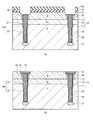
(第1の実施の形態)
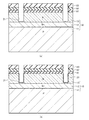
図1は、第1の実施の形態による半導体装置の構造を模式的に示す断面図である。ここでは、N+型埋め込み層12が形成されたP型のシリコン基板11の素子分離絶縁膜としてのディープトレンチ膜26で区画された素子形成領域内にLDMOSが形成された構造の半導体装置を例に挙げて説明する。
(First embodiment)
FIG. 1 is a cross-sectional view schematically showing the structure of the semiconductor device according to the first embodiment. Here, a semiconductor device having a structure in which an LDMOS is formed in an element formation region defined by a
基板10としては、N+型埋め込み層12が所定の深さに形成されたP型のシリコン基板11が用いられる。この基板10は、P型のシリコン基板11上に、N型不純物が導入されたシリコン層からなるN+型埋め込み層12と、N+型埋め込み層12よりもN型不純物の濃度が低いシリコン層からなるN型半導体層13とが形成された構造を有している。
As the
この基板10の所定の領域には、N+型埋め込み層12の下層のシリコン基板11まで到達する所定の深さのディープトレンチ20が、平面視上たとえば額縁状に形成されており、ディープトレンチ20にはシリコン酸化膜やシリコン膜などが埋め込まれ、ディープトレンチ膜26を形成している。このディープトレンチ膜26で区画される領域が素子形成領域となる。また、ディープトレンチ20の底部の下側のシリコン基板11には、P型不純物が導入されたP型拡散層27が形成される。このP型拡散層27は、素子形成領域を電気的に分離する機能を有する。
In a predetermined region of the
ディープトレンチ膜26の上部には、シリコン基板10の表面から浅い位置における隣接する領域間を絶縁する分離膜であるシャロートレンチ30が形成され、シャロートレンチ30の側面および底面には基板10を酸化して得られるシャロートレンチ側壁酸化膜31が形成され、シャロートレンチ30内にはシリコン酸化膜などからなるシャロートレンチ膜32が形成されている。
Over the
素子形成領域内のN型半導体層13の表面から所定の深さにはP型ウェル14が形成され、このP型ウェル14にLDMOSが形成されている。このP型ウェル14において、ソースが形成される領域には、P型のベース領域51が形成され、そのP型のベース領域51の表面には、N+型ソース領域52とP+型ソース領域53とが互いに接するように形成され、さらに、N+型ソース領域52とP+型ソース領域53との表面上にソース電極61が形成されている。また、ベース領域51からN+型埋め込み層12にかけて、P−型拡散層54が形成される。
A P-
一方、P型ウェル14のドレインが形成される領域には、N+型のドレイン領域55が形成され、ドレイン領域55の表面にはドレイン電極62が形成される。ドレイン領域55とベース領域51との間には、ドレイン領域55に隣接して、N−型のドリフト領域56が形成されている。さらに、ソース電極61とドレイン電極62との間のベース領域51およびP型ウェル14上には、ゲート絶縁膜71を介してゲート電極72が形成されている。
On the other hand, an N +
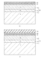
ここで、基板10に形成されるディープトレンチ20について説明する。第1の実施の形態によるディープトレンチ20は、N+型埋め込み層12よりも上の位置を境に開口径が異なっている。この図では、N+型埋め込み層12とN型半導体層13との境界付近で開口径が異なる境界を有しており、この境界よりも上側で開口径が大きく、この境界以下で開口径が小さくなっている。以下では、ディープトレンチ20の開口径が大きい部分を第1のディープトレンチ21といい、開口径が小さい部分を第2のディープトレンチ22という。
Here, the
第1のディープトレンチ21の側面を被覆するように、第1の側壁酸化膜23が形成され、第2のディープトレンチ22の側面と底面を被覆するように、第2の側壁酸化膜24が形成される。また、これらの側壁酸化膜23,24で被覆されたディープトレンチ20内には、TEOS(Tetraethyl orthosilicate)膜が埋め込まれている。さらに、第2のディープトレンチ22の周囲には、N+型埋め込み層12を拡散源としたN型拡散層25が形成される。しかし、第1のディープトレンチ21の周囲には、N型拡散層25は形成されていない。
A first
このように、N+型埋め込み層12を拡散源とするN型拡散層25は、N+型埋め込み層12の上部のN型半導体層13には形成されないので、N+型埋め込み層12の上部では、所望の不純物プロファイルを形成することができる。また、N+型埋め込み層12の下部のシリコン基板11にのみN型拡散層25は形成されるので、N+型埋め込み層12の不純物濃度勾配が緩和され、また空乏層が伸びる。その結果、素子間耐圧を改善するとともに、素子内部耐圧を向上させることができる。
As described above, the N-
つぎに、このような構造の半導体装置の製造方法について説明する。図2−1〜図2−8は、第1の実施の形態による半導体装置の製造方法の手順の一例を模式的に示す図である。まず、図2−1(a)に示されるように、基板10として、基板10表面から5μmの深さにN+型埋め込み層12を形成したP型シリコン基板11を用いる。具体的には、P型シリコン基板11上に、N+型埋め込み層12および厚さ5μmのN型半導体層13が順に形成された基板10を用いる。この基板10上に、酸化技術を用いて15nmの厚さのSiO膜からなるバッファ酸化膜81を形成し、その後、LPCVD(Low Pressure CVD)法によって200nmの厚さのSiN膜からなるストッパ膜82を形成する。バッファ酸化膜81は、後工程において、素子形成領域の保護膜として使用し、ストッパ膜82は、後工程の酸化膜のCMP処理時のストッパ膜82として利用する。
Next, a method for manufacturing a semiconductor device having such a structure will be described. 2-1 to 2-8 are schematic diagrams illustrating an example of the procedure of the method of manufacturing the semiconductor device according to the first embodiment. First, as shown in FIG. 2A, a P-
ついで、図2−1(b)に示されるように、ストッパ膜82上の全面にCVD法によってSiO系のマスク膜83を成膜する。このマスク膜83は、後の工程でのディープトレンチ20を形成する際のRIE(Reactive Ion Etching)のマスクとして使用する。そのため、このマスク膜83の厚さは、ディープトレンチ20を形成する際の溝をRIEでエッチングすることができる厚さに設定される。ここでは、1,000nmの厚さに堆積されるものとする。
Next, as shown in FIG. 2B, a SiO-based
その後、図2−2(a)に示されるように、マスク膜83上に図示しないレジストを塗布し、リソグラフィ技術を用いて、ディープトレンチ20の形成領域を決定するためのパターニングを行う。ここでは、0.7μmの開口幅を有し、概略矩形の額縁状のディープトレンチ20を形成するためのパターニングを行うものとする。ついで、パターニングされたレジストをマスクとして、マスク膜83、ストッパ膜82およびバッファ酸化膜81を、RIE法を用いてN型半導体層13に達するまでエッチングする。アッシングによってレジストを除去した後、パターニングされたマスク膜83をマスクとして、基板10をRIE法によってエッチングする。このときの基板10のエッチング量は、N+型埋め込み層12に達しない深さとし、ここでは、基板10(N型半導体層13)の表面から4μmとする。これによって、第1のディープトレンチ21が形成される。なお、これによって、マスク膜83の厚さは200nm程度となる。
Thereafter, as shown in FIG. 2A, a resist (not shown) is applied on the
ついで、図2−2(b)に示されるように、酸化技術によって、第1のディープトレンチ21の内面に露出しているシリコンを酸化して、第1のディープトレンチ21の側壁および底面に、50nmの厚さの第1の側壁酸化膜23を形成する。この第1の側壁酸化膜23は、素子分離のための絶縁膜として使用する。この第1の側壁酸化膜23を形成する時点では、第1のディープトレンチ21の底面の位置は、N+型埋め込み層12の形成位置よりも上に位置しているので、N+型埋め込み層12は露出していない。そのため、酸化によって、N+型埋め込み層12を構成するN型の不純物による外方拡散は発生しない。つまり、第1のディープトレンチ21の内壁の側面には、N+型埋め込み層12が拡散源となるN型拡散層25は形成されず、シリコン酸化膜のみによって構成される第1の側壁酸化膜23が形成される。
Next, as shown in FIG. 2B, the silicon exposed on the inner surface of the first
その後、図2−3(a)に示されるように、RIE法を用いて全面エッチングを行う。具体的には、RIE法によってエッチバックを行い、第1のディープトレンチ21の底部に形成された第1の側壁酸化膜23を除去し、第1のディープトレンチ21の側面にのみ第1の側壁酸化膜23をサイドウォールとして残す。
Thereafter, as shown in FIG. 2-3A, the entire surface is etched using the RIE method. Specifically, etch back is performed by the RIE method, the first
ついで、図2−3(b)に示されるように、200nm程度残されたマスク膜83をマスクとして、RIE法によって、自己整合的に第2のディープトレンチ22を第1のディープトレンチ21の下部に形成する。この第2のディープトレンチ22の深さは、第1のディープトレンチ21の深さ(4μm)と合わせて、10μmとなるようにする。これによって、第1のディープトレンチ21と第2のディープトレンチ22とによって構成されるディープトレンチ20が形成される。
Next, as shown in FIG. 2B, the second
第2のディープトレンチ22を形成した後、図2−4(a)に示されるように、酸化技術によって、第2のディープトレンチ22の内面(側面と底面)に50nmの厚さの第2の側壁酸化膜24を形成する。この酸化処理では、N+型埋め込み層12は、第2のディープトレンチ22の形成によって表面に露出している状態であるので、酸化処理時に外方拡散が発生する。その結果、第2のディープトレンチ22の内壁には、N+型埋め込み層12を拡散源としたN型拡散層25が形成される。しかし、N+型埋め込み層12よりも上部の第1のディープトレンチ21の側壁は、第1の側壁酸化膜23(サイドウォール)によって表面が保護されているため、シリコンまでは拡散されない。これによって、ディープトレンチ20において、第2のディープトレンチ22の側面の周囲にのみN型拡散層25が形成される。その後、ディープトレンチ20の底部に、素子分離の耐圧を向上させるために、イオン注入を行ってP型拡散層27を形成する。ここでは、ホウ素(B)を注入してP型拡散層27を形成する。
After forming the second
ついで、図2−4(b)に示されるように、ディープトレンチ20を形成したマスク膜83上の全面に、LPCVD法によって500nmの厚さのTEOS膜を形成する。これによって、マスク膜83上にTEOS膜が成膜されるとともに、ディープトレンチ20内にTEOS膜が埋め込まれる。その後、マスク膜83上に形成されたTEOS膜をCMP法によって除去し、平坦化する。さらに、RIE法によって、ストッパ膜82をストッパとして、TEOS膜をエッチングする。具体的には、TEOS膜をストッパ膜82よりもエッチングされやすい条件で、ストッパ膜82の表面が露出するまでエッチングを行う。これによって、ディープトレンチ20内にTEOS膜からなるディープトレンチ膜26が形成される。
Next, as shown in FIG. 2-4 (b), a TEOS film having a thickness of 500 nm is formed on the entire surface of the
その後、ストッパ膜82上にシャロートレンチ30加工のマスク材となる図示しないマスク材絶縁膜をたとえば100nmの厚さで形成し、マスク材絶縁膜上に図示しないレジストを塗布し、リソグラフィ技術によってアクティブ領域を分離するシャロートレンチ30を形成するためのパターニングを行う。
Thereafter, a mask material insulating film (not shown) serving as a mask material for processing the
ついで、図2−5(a)に示されるように、このパターニングしたレジストをマスクとして、マスク材絶縁膜、ストッパ膜82およびバッファ酸化膜81をRIE法によってエッチングし、シャロートレンチ形成用のパターンをマスク材絶縁膜に転写する。レジストをアッシングで除去した後、マスク材絶縁膜をマスクとして、基板10(N型半導体層13)をエッチングし、シャロートレンチ30を形成する。この深さは、0.4μmとする。なお、N+型埋め込み層12の上面から基板10の表面までは、5μm程度あるので、このシャロートレンチ30の深さは十分に浅い。このとき、ディープトレンチ20内のTEOS膜もシャロートレンチ30の加工時に同時にエッチングされるので、ディープトレンチ20の上部にもシャロートレンチ30が形成される。
Next, as shown in FIG. 2-5 (a), using this patterned resist as a mask, the mask material insulating film, the
ついで、図2−5(b)に示されるように、シャロートレンチ30の側壁を保護することを目的に酸化技術によって50nmの厚さのシャロートレンチ側壁酸化膜31を形成する。その後、LPCVD法によってシャロートレンチ30内をTEOS膜で埋め込む。成膜後に発生する段差は、CMP法によってストッパ膜82をストッパとして平坦化する。CMP処理の後、不要となったストッパ膜82を、熱燐酸などを用いたウェットエッチング法によって除去する。これによって、シャロートレンチ30内にシャロートレンチ膜32が形成される。以上によって、ディープトレンチ膜26とシャロートレンチ膜32とによって区画された基板10上の領域が素子形成領域となる。そして、イオン注入法によって、素子形成領域内にBなどのP型不純物を打ち込み、活性化させて、N型半導体層13の下面よりも浅い領域にP型ウェル14を形成する。
Next, as shown in FIG. 2B, a shallow trench
この後、素子形成領域上へのLDMOSの形成が行われる。まず、図2−6(a)に示されるように、ディープトレンチ膜26を形成した基板10上の全面にレジスト84を塗布し、リソグラフィ技術によって、ソース領域形成領域付近に開口部を有するようにパターニングを行う。そして、イオン注入法によって、基板10表面からN+型埋め込み層12にかけてBなどのP型不純物を導入し、活性化させてP−型拡散層54を形成する。
Thereafter, LDMOS is formed on the element formation region. First, as shown in FIG. 2-6 (a), a resist 84 is applied to the entire surface of the
レジスト84をアッシングなどの方法で除去した後、図2−6(b)に示されるように、基板10上の全面にレジスト85を塗布し、ベース領域51に開口部を有するようにリソグラフィ技術によってパターニングを行う。そして、イオン注入法によって、基板10表面からP型ウェル14内の所定の深さにかけてBなどのP型不純物を導入し、活性化させ、ベース領域51を形成する。このとき、ベース領域51のP型不純物濃度は、P−型拡散層54よりも高くなるように調節される。
After removing the resist 84 by a method such as ashing, as shown in FIG. 2-6 (b), a resist 85 is applied to the entire surface of the
レジスト85をアッシングなどの方法で除去した後、基板10上に絶縁膜とポリシリコン膜などの導電性材料膜とを積層する。導電性材料膜上に図示しないレジストを塗布し、ゲート電極形状にパターニングを行った後、RIE法などの方法でレジストをマスクとしてエッチングを行う。これによって、図2−7(a)に示されるように、基板10上にゲート絶縁膜71とゲート電極72とが形成される。ここでは、ゲート絶縁膜71とゲート電極72お積層体は、P型ウェル14とベース領域51との境界をまたぐように形成される。
After removing the resist 85 by a method such as ashing, an insulating film and a conductive material film such as a polysilicon film are stacked on the
ついで、図2−7(b)に示されるように、ゲート電極72を形成した基板10上にレジスト86を塗布し、ドリフト領域56およびドレイン領域55が開口するようにリソグラフィ技術によってパターニングを行う。そして、イオン注入法によって、基板10表面から所定の深さまでPなどのN型不純物を導入し、活性化させ、ドリフト領域56を形成する。
Next, as shown in FIG. 2B, a resist 86 is applied on the
レジスト86をアッシングなどの方法で除去した後、図2−8(a)に示されるように、基板10上にレジスト88を塗布し、ドレイン領域55およびN+型ソース領域52が開口するように、リソグラフィ技術によってパターニングを行う。そして、イオン注入法によって、基板10表面から所定の深さまでPなどのN型不純物を導入し、活性化させ、ドレイン領域55およびN+型ソース領域52を形成する。このときのN型不純物濃度は、ドリフト領域56よりも高くなるように調節される。
After removing the resist 86 by a method such as ashing, as shown in FIG. 2-8 (a), a resist 88 is applied on the
レジスト87をアッシングなどの方法で除去した後、図2−8(b)に示されるように、基板10上にレジスト88を塗布し、P+型ソース領域53が開口するように、リソグラフィ技術によってパターニングを行う。そして、イオン注入法によって、基板10表面から所定の深さまでBなどのP型不純物を導入し、活性化させ、P+型ソース領域53を形成する。
After removing the resist 87 by a method such as ashing, as shown in FIG. 2-8 (b), a resist 88 is applied on the
レジスト88をアッシングなどの方法で除去した後、たとえばレジストを基板10上に塗布し、ドレイン領域55の一部と、N+型ソース領域52とP+型ソース領域53の一部が開口するようにリソグラフィ技術によってパターニングを行う。そして、導電性材料膜を開口部内に形成し、レジストを除去する。これによって、図1に示されるように、ソース電極61およびドレイン電極62が形成される。以上によって、LDMOSが製造される。
After removing the resist 88 by a method such as ashing, for example, a resist is applied onto the
図3は、ディープトレンチの構成の違いによる素子間耐圧および素子内部耐圧の一例を示す図である。ここでは、最小寸法が0.13μmのデバイス製造技術を用いて形成されたLDMOSを用いて測定を行っている。比較例1は、特許文献1のように、ディープトレンチの側壁に酸化膜を形成する際に、ディープトレンチの側壁に沿ってN+型埋め込み層を拡散源とするN型拡散層が形成された場合を示し、比較例2は、比較例1の場合でN型拡散層の外方拡散を抑える条件で酸化を行った場合を示している。また、縦軸は耐圧[V]を示している。
FIG. 3 is a diagram illustrating an example of an inter-device breakdown voltage and an element internal breakdown voltage due to a difference in the configuration of the deep trench. Here, the measurement is performed using an LDMOS formed using a device manufacturing technique having a minimum dimension of 0.13 μm. In Comparative Example 1, as in
比較例1では、N+型埋め込み層の不純物が拡散することによって、N+型埋め込み層の不純物濃度勾配を緩和し、N+型埋め込み層の下部では空乏層が伸びることで、素子間耐圧が改善するが、N+型埋め込み層の上部では空乏層の伸びが抑えられるため、素子内部耐圧が低下している。また、比較例2では、酸化条件によってN+型埋め込み層の外方拡散を抑制している結果、比較例1とは逆に、素子内部耐圧は向上しているが、素子間耐圧が低下してしまっている。 In Comparative Example 1, the impurity concentration gradient of the N + type buried layer is relaxed by diffusing impurities in the N + type buried layer, and the depletion layer extends below the N + type buried layer, thereby improving the breakdown voltage between elements. In the upper part of the N + type buried layer, the depletion layer is prevented from growing, so that the internal breakdown voltage of the element is lowered. Further, in Comparative Example 2, as a result of suppressing the outward diffusion of the N + type buried layer depending on the oxidation condition, contrary to Comparative Example 1, the internal breakdown voltage is improved, but the inter-element breakdown voltage is decreased. I'm stuck.
一方、第1の実施の形態では、ディープトレンチ20を、N+型埋め込み層12よりも上の第1のディープトレンチ21と、その下部に形成され、N+型埋め込み層12よりも深い位置に底部を有する第2のディープトレンチ22と、を別々形成した。具体的には、第1のディープトレンチ21の側壁に沿って第1の側壁酸化膜23のみを形成し、その後に、第2のディープトレンチ22の側壁に沿って第2の側壁酸化膜24を形成するとともに、その外側にN+型埋め込み層12を拡散源とするN型拡散層25を形成した。これによって、比較例1のように素子間耐圧を改善するとともに、比較例2のように素子内部耐圧も向上させることができるという効果を有する。
On the other hand, in the first embodiment, the
また、ディープトレンチ20の形成時において、第1のディープトレンチ21の底部がN+型埋め込み層12の上面よりも上の位置となるようにして第1のディープトレンチ21を形成したので、第1のディープトレンチ21の側壁に第1の側壁酸化膜23を形成する際に、N+型埋め込み層12のN型不純物が第1のディープトレンチ21の周囲に拡散することがない。さらに、第2のディープトレンチ22を形成後に、酸化処理を行っても、第1のディープトレンチ21の側壁には第1の側壁酸化膜23が形成されているので、N+型埋め込み層12のN型不純物が第1のディープトレンチ21の側壁の周囲に拡散することもない。
Further, when the
また、第1のディープトレンチ21を形成したマスク膜83を用いて、第2のディープトレンチ22を形成するようにしたので、第1と第2のディープトレンチ21,22を形成するために別個のリソグラフィ工程を行うことなく、従来のディープトレンチ20の製造工程に最小限の工程の追加のみで、ディープトレンチ20の側面に形成される不純物層の制御が可能となる。
In addition, since the second
(第2の実施の形態)
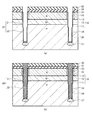
図4は、第2の実施の形態による半導体装置の構造を模式的に示す断面図である。ここでは、N+型埋め込み層12が形成されたP型のシリコン基板11のディープトレンチ20膜で区画された素子形成領域内に高周波半導体装置が形成された構造の半導体装置を例に挙げて説明する。
(Second Embodiment)
FIG. 4 is a cross-sectional view schematically showing the structure of the semiconductor device according to the second embodiment. Here, a semiconductor device having a structure in which a high-frequency semiconductor device is formed in an element formation region defined by a
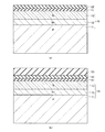
基板10としては、N+型埋め込み層12が所定の深さに形成されたP型のシリコン基板11が用いられる。この基板10は、第1の実施の形態と同様に、P型のシリコン基板11上に、N+型埋め込み層12と、N型半導体層13とが形成された構造を有しているが、N型半導体層13の厚さが第1の実施の形態とは異なり、薄くなっている。たとえば、N型半導体層13の厚さ(基板10の表面からN+型埋め込み層12の上面までの距離)は、第1の実施の形態では5μm程度であるのに対して、第2の実施の形態では1μm程度である。
As the
この基板10の所定の領域には、N+型埋め込み層12の下層のシリコン基板11まで到達する所定の深さのディープトレンチ20が、平面視上たとえば額縁状に形成されており、ディープトレンチ20にはシリコン酸化膜やシリコン膜などが埋め込まれ、ディープトレンチ膜26を形成している。このディープトレンチ膜26で区画される領域が素子形成領域となる。また、ディープトレンチ20の底部の下側のシリコン基板11には、素子形成領域を電気的に分離するP型不純物が導入されたP型拡散層27が形成される。
In a predetermined region of the
ディープトレンチ膜26の上部には、シャロートレンチ30が形成され、シャロートレンチ30の側面および底面には基板10を酸化して得られるシャロートレンチ側壁酸化膜31が形成され、シャロートレンチ30内にはシリコン酸化膜などからなるシャロートレンチ膜32が形成されている。
A
素子形成領域内には、高周波半導体装置としてNPNバイポーラトランジスタが形成されている。具体的には、素子形成領域内のN型半導体層13には、N+型埋め込み層12に達するN型のコレクタ領域101が形成されている。また、N型半導体層13の上部には、コレクタ領域101の形成位置とN型半導体層13によって分離されるP型のベース領域102が形成されている。また、ベース領域102の上部にはN型のエミッタ領域103が形成されている。そして、コレクタ領域101、ベース領域102およびエミッタ領域103上には、それぞれ、コレクタ電極111、ベース電極112およびエミッタ電極113が形成されている。
In the element formation region, an NPN bipolar transistor is formed as a high-frequency semiconductor device. Specifically, an N-
ここで、基板に形成されるディープトレンチ20について説明する。第2の実施の形態によるディープトレンチ20は、N+型埋め込み層12よりも下の位置を境に開口径が異なっている。この図では、N+型埋め込み層12よりも下のシリコン基板11内で開口径が異なる境界を有しており、この境界よりも上側で開口径が大きく、この境界以下で開口径が小さくなっている。以下では、ディープトレンチ20の開口径が大きい部分を第1のディープトレンチ21といい、開口径が小さい部分を第2のディープトレンチ22という。
Here, the
第1のディープトレンチ21の側面を被覆するように、第1の側壁酸化膜23が形成され、第2のディープトレンチ22の側面と底面を被覆するように、第2の側壁酸化膜24が形成される。また、これらの側壁酸化膜23,24で被覆されたディープトレンチ20内には、TEOS膜が埋め込まれている。さらに、第1のディープトレンチ21の周囲には、N+型埋め込み層12を拡散源としたN型拡散層25が形成される。しかし、第2のディープトレンチ22の周囲には、N型拡散層25は形成されていない。
A first
このように、N+型埋め込み層12を拡散源とするN型拡散層25は、N+型埋め込み層12の下部のP型シリコン基板11には形成されないので、N+型埋め込み層12の下部では、空乏層の伸びが抑えられる。その結果、素子間耐圧は、第1の実施の形態に比して劣る。しかし、N+型埋め込み層12の上部では、空乏層の伸びが生じるので、素子内部の耐圧を向上させることができる。
As described above, the N-
つぎに、このような構造の半導体装置の製造方法について説明する。図5−1〜図5−7は、第2の実施の形態による半導体装置の製造方法の手順の一例を模式的に示す図である。まず、図5−1(a)に示されるように、基板10として、基板表面から1μmの深さにN+型埋め込み層12を形成したP型シリコン基板11を用いる。具体的には、P型シリコン基板11上に、N+型埋め込み層12および厚さ1μmのN型半導体層13が順に形成された基板10を用いる。この基板10上に、酸化技術を用いて15nmの厚さのSiO膜からなるバッファ酸化膜81を形成し、その後、LPCVD法によって200nmの厚さのSiN膜からなるストッパ膜82を形成する。バッファ酸化膜81は、後工程において、素子形成領域の保護膜として使用し、ストッパ膜82は、後工程の酸化膜のCMP処理時のストッパ膜82として利用する。
Next, a method for manufacturing a semiconductor device having such a structure will be described. FIGS. 5-1 to 5-7 are diagrams schematically illustrating an example of the procedure of the method of manufacturing the semiconductor device according to the second embodiment. First, as shown in FIG. 5A, a P-
ついで、図5−1(b)に示されるように、ストッパ膜82上の全面にCVD法によってSiO系のマスク膜83を成膜する。このマスク膜83は、後の工程でのディープトレンチ20を形成する際のRIEのマスクとして使用する。そのため、ディープトレンチ20を形成する際の溝をRIEでエッチングすることができる厚さに設定される。ここでは、1,000nmの厚さに堆積されるものとする。
Next, as shown in FIG. 5B, a SiO-based
その後、図5−2(a)に示されるように、マスク膜83上に図示しないレジストを塗布し、リソグラフィ技術を用いて、ディープトレンチ20の形成領域を決定するためのパターニングを行う。ここでは、ディープトレンチ20の開口幅を0.7μmとする。ついで、パターニングされたレジストをマスクとして、マスク膜83、ストッパ膜82およびバッファ酸化膜81を、RIE法を用いてN型半導体層13に達するまでエッチングする。アッシングによってレジストを除去した後、パターニングされたマスク膜83をマスクとして、N型半導体層13、N+型埋め込み層12およびP型シリコン基板11をRIE法によってエッチングする。このときの基板10のエッチング量は、N+型埋め込み層12の底部(下面)よりも深い深さとし、ここでは、基板10(N型半導体層13)の表面から2μmとする。これによって、第1のディープトレンチ21が形成される。なお、これによって、マスク膜83の厚さは200nm程度となる。
Thereafter, as shown in FIG. 5A, a resist (not shown) is applied on the
ついで、図5−2(b)に示されるように、酸化技術によって、第1のディープトレンチ21の内面に露出しているシリコンを酸化して、第1のディープトレンチ21の側壁および底面に、50nmの厚さの第1の側壁酸化膜23を形成する。この第1の側壁酸化膜23は、素子分離のための絶縁膜として使用する。この第1の側壁酸化膜23を形成する時点で、第1のディープトレンチ21の内壁には、N+型埋め込み層12が露出しているので、酸化によってN+型埋め込み層12を構成するN型の不純物による外方拡散が発生する。その結果、第1のディープトレンチ21の側面の内部には、基板10の酸化によって第1の側壁酸化膜23が形成されるとともに、第1のディープトレンチ21の側面の外周には、N+型埋め込み層12を拡散源とするN型拡散層25が形成される。
Next, as shown in FIG. 5B, the silicon exposed on the inner surface of the first
その後、図5−3(a)に示されるように、RIE法を用いて全面エッチングを行う。具体的には、RIE法によってエッチバックを行い、第1のディープトレンチ21の底部に形成された第1の側壁酸化膜23を除去し、第1のディープトレンチ21の側面にのみ第1の側壁酸化膜23をサイドウォールとして残す。
Thereafter, as shown in FIG. 5-3 (a), the entire surface is etched by using the RIE method. Specifically, etch back is performed by the RIE method, the first
ついで、図5−3(b)に示されるように、200nm程度残されたマスク膜83をマスクとして、RIE法によって、自己整合的に第2のディープトレンチ22を第1のディープトレンチ21の下部に形成する。この第2のディープトレンチ22の深さは、第1のディープトレンチ21の深さ(2μm)と合わせて、5μmとなるようにする。これによって、第1のディープトレンチ21と第2のディープトレンチ22とによって構成されるディープトレンチ20が形成される。
Next, as shown in FIG. 5B, the second
第2のディープトレンチ22を形成した後、図5−4(a)に示されるように、酸化技術によって、第2のディープトレンチ22の内面(側面と底面)に50nmの厚さの第2の側壁酸化膜24を形成する。N+型埋め込み層12は、第2のディープトレンチ22の形成によって表面に露出していない状態であるので、この酸化処理では、N+型埋め込み層12を構成するN型の不純物による外方拡散は発生しない。つまり、第2のディープトレンチ22の内壁の側面には、N+型埋め込み層12を拡散源とするN型拡散層25は形成されず、基板10のプロファイルが維持され、シリコン酸化膜のみによって構成される第2の側壁酸化膜24が形成される。その後、ディープトレンチ20の底部に、素子分離の耐圧を向上させるために、BなどのP型不純物のイオン注入を行ってP型拡散層27を形成する。
After forming the second
ついで、図5−4(b)に示されるように、ディープトレンチ20を形成したマスク膜83上の全面に、LPCVD法によって500nmの厚さのTEOS膜を形成する。これによって、マスク膜83上にTEOS膜が成膜されるとともに、ディープトレンチ20内にTEOS膜が埋め込まれる。その後、マスク膜83上に形成されたTEOS膜をCMP法によって除去し、平坦化する。さらに、RIE法によって、ストッパ膜82をストッパとして、TEOS膜をエッチングする。具体的には、TEOS膜をストッパ膜82よりもエッチングされやすい条件で、ストッパ膜82の表面が露出するまでエッチングを行う。これによって、ディープトレンチ20内にTEOS膜からなるディープトレンチ膜26が形成される。
Next, as shown in FIG. 5-4 (b), a TEOS film having a thickness of 500 nm is formed on the entire surface of the
その後、ストッパ膜82上にシャロートレンチ30加工のマスク材となる図示しないマスク材絶縁膜をたとえば100nmの厚さで形成し、マスク材絶縁膜上に図示しないレジストを塗布し、リソグラフィ技術によってアクティブ領域を分離するシャロートレンチ30を形成するためのパターニングを行う。
Thereafter, a mask material insulating film (not shown) serving as a mask material for processing the
ついで、図5−5(a)に示されるように、このパターニングしたレジストをマスクとして、マスク材絶縁膜、ストッパ膜82およびバッファ酸化膜81をRIE法によってエッチングし、シャロートレンチ形成用のパターンをマスク材絶縁膜に転写する。レジストをアッシングで除去した後、マスク材絶縁膜をマスクとして、基板10(N型半導体層13)をエッチングし、シャロートレンチ30を形成する。この深さは、0.3μmとする。なお、N+型埋め込み層12の上面から基板10の表面までは、1μm程度あるので、このシャロートレンチ30の深さは十分に浅い。このとき、ディープトレンチ20内のTEOS膜もシャロートレンチ30の加工時に同時にエッチングされるので、ディープトレンチ20の上部にもシャロートレンチ30が形成される。
Next, as shown in FIG. 5-5 (a), using the patterned resist as a mask, the mask material insulating film, the
ついで、図5−5(b)に示されるように、シャロートレンチ30の側壁を保護することを目的に酸化技術によって50nmの厚さのシャロートレンチ側壁酸化膜31を形成する。その後、LPCVD法によってシャロートレンチ30内をTEOS膜で埋め込む。成膜後に発生する段差は、CMP法によってストッパ膜82をストッパとして平坦化する。CMP処理の後、不要となったストッパ膜82を、熱燐酸などを用いたウェットエッチング法によって除去する。これによって、ディープトレンチ膜26とシャロートレンチ膜32とによって区画された基板10上の領域が素子形成領域となる。
Next, as shown in FIG. 5B, a shallow trench
この後、素子形成領域上への高周波半導体素子の形成が行われる。まず、図5−6(a)に示されるように、ディープトレンチ膜26を形成した基板10上の全面にレジスト121を塗布し、リソグラフィ技術によって、コレクタ領域101に開口部を有するようにパターニングを行う。そして、イオン注入法によって、基板10表面からN+型埋め込み層12にかけてPなどのN型不純物を導入し、活性化させてコレクタ領域101を形成する。
Thereafter, a high-frequency semiconductor element is formed on the element formation region. First, as shown in FIG. 5-6 (a), a resist 121 is applied to the entire surface of the
レジスト121をアッシングなどの方法で除去した後、図5−6(b)に示されるように、基板10上の全面にレジスト122を塗布し、ベース領域102に開口部を有するようにリソグラフィ技術によってパターニングを行う。そして、イオン注入法によって、基板10表面からN型半導体層13内の所定の深さにかけてBなどのP型不純物を導入し、活性化させ、ベース領域102を形成する。このとき、ベース領域102は、コレクタ領域101から所定の距離をおいて形成される。
After removing the resist 121 by a method such as ashing, as shown in FIG. 5-6 (b), a resist 122 is applied to the entire surface of the
レジスト122をアッシングなどの方法で除去した後、図5−7に示されるように、基板10上の全面にレジスト123を塗布し、ベース領域102内に開口部を有するようにリソグラフィ技術によってパターニングを行う。そして、イオン注入法によって、基板10表面からベース領域102内の所定の深さにかけてPなどのN型不純物を導入し、活性化させ、エミッタ領域103を形成する。
After removing the resist 122 by a method such as ashing, as shown in FIG. 5-7, a resist 123 is applied to the entire surface of the
レジスト123をアッシングなどの方法で除去した後、基板10上の全面に導電性材料膜を形成し、さらにその上にレジストを塗布する。リソグラフィ技術によって、コレクタ領域101、ベース領域102およびエミッタ領域103上にそれぞれコレクタ電極111、ベース電極112およびエミッタ電極113を形成するためのパターンを形成する。その後、RIE法によって、レジストをマスクとして導電性材料膜のエッチングを行う。これによって、図4に示されるように、コレクタ電極111、ベース電極112およびエミッタ電極113が、それぞれコレクタ領域101、ベース領域102およびエミッタ領域103上に形成される。以上によって、高周波半導体装置としてのNPNトランジスタが製造される。
After removing the resist 123 by a method such as ashing, a conductive material film is formed on the entire surface of the
図6は、ディープトレンチの構成の違いによるコレクタ−基板間の容量の一例を示す図である。ここでは、最小寸法が0.13μmのデバイス製造技術を用いて形成された高周波半導体層値を用いて測定を行っている。また、コレクタ−基板間の容量は、コレクタ領域101−シリコン基板11間のPN接合による第1の容量と、ディープトレンチ20を介した第2の容量とに分類することができる。比較例3は、特許文献1のように、ディープトレンチ20の側壁に酸化膜を形成する際に、最終的な深さまでディープトレンチを形成し、N+型埋め込み層を露出させた状態で酸化処理を行って、N+型埋め込み層を拡散源とするN型拡散層がディープトレンチの側壁に沿って形成された場合を示している。
FIG. 6 is a diagram illustrating an example of the capacitance between the collector and the substrate due to the difference in the configuration of the deep trench. Here, the measurement is performed using a high-frequency semiconductor layer value formed using a device manufacturing technique with a minimum dimension of 0.13 μm. The capacity between the collector and the substrate can be classified into a first capacity due to a PN junction between the
第2の実施の形態によるディープトレンチ20では、N+型埋め込み層12よりも下部のN型拡散層25の形成が抑制されているので、空乏層の伸びが抑えられる。その結果、比較例3に比較して容量が低下し、高周波特性の改善が可能となるという効果を有する。
In the
なお、上述した説明では、P型の半導体基板にN+型埋め込み層12を有する場合を例に挙げて説明したが、逆にN型の半導体基板にP型の埋め込み層を有するものに、上述した実施の形態を適用してもよい。また、半導体基板としては、シリコン基板11に限られず、他のガリウムヒ素などの半導体基板を用いることができる。
In the above description, the case where the P + type semiconductor substrate has the N + type buried
10…基板、11…P型シリコン基板、12…N+型埋め込み層、13…N型半導体層、14…P型ウェル、20…ディープトレンチ、21…第1のディープトレンチ、22…第2のディープトレンチ、23…第1の側壁酸化膜、24…第2の側壁酸化膜、25…N型拡散層、26…ディープトレンチ膜、30…シャロートレンチ、31…シャロートレンチ側壁酸化膜、32…シャロートレンチ膜、51,102…ベース領域、52…N+型ソース領域、53…P+型ソース領域、54…P−型拡散層、55…N+型ドレイン領域、56…ドリフト領域、61…ソース電極、62…ドレイン電極、71…ゲート絶縁膜、72…ゲート電極、101…コレクタ領域、103…エミッタ領域、111…コレクタ電極、112…ベース電極、113…エミッタ電極。
DESCRIPTION OF
Claims (5)
前記基板に、前記埋め込み層の形成位置よりも深く形成され、前記基板内の素子形成領域内を区画するトレンチと、
前記トレンチの内壁に沿って形成される側壁酸化膜と、前記側壁酸化膜で被覆された前記トレンチ内を埋める埋め込み膜と、を含む素子分離絶縁膜と、
前記素子分離絶縁膜で区画される素子形成領域に形成される半導体素子と、
を備え、
前記トレンチは、前記基板表面から所定の境界深さまでの第1のトレンチと、前記境界深さから底部までの前記第1のトレンチよりも小さい開口径を有する第2のトレンチによって構成され、
前記半導体素子は、
前記素子形成領域の前記半導体層の表面に形成される所定の導電型の不純物拡散層からなるソース領域と、
前記素子形成領域の前記半導体層の表面に前記ソース領域から離れて形成され、所定の導電型の不純物拡散層からなるドレイン領域と、
前記ソース領域と前記ドレイン領域との間で、前記半導体層上にゲート絶縁膜を介して形成されるゲート電極と、
前記ドレイン領域から前記ゲート電極の下部にかけて、前記ドレイン領域に隣接して形成され、前記ドレイン領域の不純物濃度よりも低い濃度の不純物拡散層からなる前記第2の導電型のドリフト領域と、
前記ソース領域に接続されるソース電極と、
前記ドレイン領域に接続されるドレイン電極と、
を有し、
前記トレンチの境界深さは前記半導体層内にあり、
前記第2のトレンチの側壁の周囲にのみ前記埋め込み層に接続される第1の拡散層が形成されることを特徴とする半導体装置。 A second conductivity type buried layer on a first conductivity type semiconductor substrate, and the second conductivity type semiconductor having a predetermined thickness in which the impurity concentration of the second conductivity type is lower than that of the buried layer. A substrate on which a layer is laminated;
A trench that is formed deeper than the formation position of the buried layer in the substrate and defines an element formation region in the substrate;
An element isolation insulating film including a sidewall oxide film formed along the inner wall of the trench, and a buried film filling the trench covered with the sidewall oxide film;
A semiconductor element formed in an element formation region partitioned by the element isolation insulating film;
With
The trench is constituted by a first trench from the substrate surface to a predetermined boundary depth, and a second trench having an opening diameter smaller than the first trench from the boundary depth to the bottom,
The semiconductor element is
A source region comprising an impurity diffusion layer of a predetermined conductivity type formed on the surface of the semiconductor layer in the element formation region;
A drain region formed of an impurity diffusion layer of a predetermined conductivity type formed on the surface of the semiconductor layer of the element formation region away from the source region;
A gate electrode formed on the semiconductor layer via a gate insulating film between the source region and the drain region;
A drift region of the second conductivity type formed of an impurity diffusion layer formed adjacent to the drain region from the drain region to the lower portion of the gate electrode and having a concentration lower than the impurity concentration of the drain region;
A source electrode connected to the source region;
A drain electrode connected to the drain region;
Have
The trench boundary depth is in the semiconductor layer;
Wherein a first diffusion layer connected to said buried layer only around the side wall of the pre-Symbol second trench is formed.
前記基板に、前記埋め込み層の形成位置よりも深く形成され、前記基板内の素子形成領域内を区画するトレンチと、
前記トレンチの内壁に沿って形成される側壁酸化膜と、前記側壁酸化膜で被覆された前記トレンチ内を埋める埋め込み膜と、を含む素子分離絶縁膜と、
前記素子分離絶縁膜で区画される素子形成領域に形成される半導体素子と、
を備え、
前記トレンチは、前記基板表面から所定の境界深さまでの第1のトレンチと、前記境界深さから底部までの前記第1のトレンチよりも小さい開口径を有する第2のトレンチによって構成され、
前記半導体素子は、
前記素子形成領域内の前記第2の導電型の半導体層の表面から前記埋め込み層にかけて形成されるコレクタ領域と、
前記素子形成領域内の前記コレクタ層の形成位置とは異なる前記半導体層の表面に形成される前記第1の導電型のベース領域と、
前記ベース領域内に形成される前記第2の導電型のエミッタ領域と、
前記コレクタ領域に接続されるコレクタ電極と、
前記ベース電極に接続されるベース電極と、
前記エミッタ領域に接続されるエミッタ電極と、
を有し、
前記トレンチの境界深さは前記埋め込み層よりも下の前記半導体基板内にあり、
前記第1のトレンチの側壁の周囲にのみ前記埋め込み層に接続される第1の拡散層が形成されることを特徴とする半導体装置。 A second conductivity type buried layer on a first conductivity type semiconductor substrate, and the second conductivity type semiconductor having a predetermined thickness in which the impurity concentration of the second conductivity type is lower than that of the buried layer. A substrate on which a layer is laminated;
A trench that is formed deeper than the formation position of the buried layer in the substrate and defines an element formation region in the substrate;
An element isolation insulating film including a sidewall oxide film formed along the inner wall of the trench, and a buried film filling the trench covered with the sidewall oxide film;
A semiconductor element formed in an element formation region partitioned by the element isolation insulating film;
With
The trench is constituted by a first trench from the substrate surface to a predetermined boundary depth, and a second trench having an opening diameter smaller than the first trench from the boundary depth to the bottom,
The semiconductor element is
A collector region formed from the surface of the second conductivity type semiconductor layer in the element formation region to the buried layer;
A base region of the first conductivity type formed on the surface of the semiconductor layer different from the formation position of the collector layer in the element formation region;
An emitter region of the second conductivity type formed in the base region;
A collector electrode connected to the collector region;
A base electrode connected to the base electrode;
An emitter electrode connected to the emitter region;
Have
The trench has a boundary depth in the semiconductor substrate below the buried layer;
A semiconductor device, wherein a first diffusion layer connected to the buried layer is formed only around the side wall of the first trench.
前記マスク膜上にレジストを塗布し、形成するトレンチの部分が開口するようにパターニングを行ってレジストパターンを形成する工程と、
前記レジストパターンを前記マスク膜に転写する工程と、
前記パターンが形成されたマスク膜を用いて、前記埋め込み層よりも浅くなるように前記半導体層をエッチングし、第1のトレンチを形成する工程と、
酸化処理を行って、前記第1のトレンチの側壁に第1の側壁酸化膜を形成する工程と、
前記マスク膜を用いて、前記埋め込み層よりも下部の前記半導体基板内の所定の深さまでエッチングし、第2のトレンチを形成する工程と、
酸化処理を行って、前記第2のトレンチの側壁に第2の側壁酸化膜を形成するとともに、前記埋め込み層中の前記第2の導電型の不純物が拡散した拡散層を形成する工程と、
前記第1および第2のトレンチ内に絶縁膜を埋め込み、前記基板内の所定の素子形成領域を囲む素子分離絶縁膜を形成する工程と、
前記素子分離絶縁膜で囲まれた前記素子形成領域内にLDMOSを形成する工程と、
を含むことを特徴とする半導体装置の製造方法。 A stopper film and a mask film are formed on a substrate in which a second conductive type buried layer and a second conductive type semiconductor layer having a predetermined thickness are stacked on a first conductive type semiconductor substrate. Forming a step;
Applying a resist on the mask film and patterning so as to open a portion of a trench to be formed, and forming a resist pattern;
Transferring the resist pattern to the mask film;
Etching the semiconductor layer so as to be shallower than the buried layer using the mask film in which the pattern is formed, and forming a first trench;
Performing an oxidation treatment to form a first sidewall oxide film on the sidewall of the first trench;
Etching to a predetermined depth in the semiconductor substrate below the buried layer using the mask film to form a second trench;
Performing an oxidation process to form a second sidewall oxide film on the sidewall of the second trench, and forming a diffusion layer in which the impurity of the second conductivity type in the buried layer is diffused;
Embedding an insulating film in the first and second trenches, and forming an element isolation insulating film surrounding a predetermined element forming region in the substrate;
Forming an LDMOS in the element formation region surrounded by the element isolation insulating film;
A method for manufacturing a semiconductor device, comprising:
前記マスク膜上にレジストを塗布し、形成するトレンチの部分が開口するようにパターニングを行ってレジストパターンを形成する工程と、
前記レジストパターンを前記マスク膜に転写する工程と、
前記パターンが形成されたマスク膜を用いて、前記埋め込み層よりも深くなるように前記半導体層、前記埋め込み層および前記半導体基板をエッチングし、第1のトレンチを形成する工程と、
酸化処理を行って、前記第1のトレンチの側壁に第1の側壁酸化膜を形成するとともに、前記埋め込み層中の前記第2の導電型の不純物が拡散した拡散層を形成する工程と、
前記マスク膜を用いて、前記第1のトレンチの底面よりも下部の前記半導体基板を所定の深さまでエッチングし、第2のトレンチを形成する工程と、
酸化処理を行って、前記第2のトレンチの側壁に第2の側壁酸化膜を形成する工程と、
前記第1および第2のトレンチ内に絶縁膜を埋め込み、前記基板内の所定の素子形成領域を囲む素子分離絶縁膜を形成する工程と、
前記素子分離絶縁膜で囲まれた前記素子形成領域内に高周波半導体素子を形成する工程と、
を含むことを特徴とする半導体装置の製造方法。 A stopper film and a mask film are formed on a substrate in which a second conductive type buried layer and a second conductive type semiconductor layer having a predetermined thickness are stacked on a first conductive type semiconductor substrate. Forming a step;
Applying a resist on the mask film and patterning so as to open a portion of a trench to be formed, and forming a resist pattern;
Transferring the resist pattern to the mask film;
Etching the semiconductor layer, the buried layer and the semiconductor substrate so as to be deeper than the buried layer using the mask film in which the pattern is formed, and forming a first trench;
Performing an oxidation process to form a first sidewall oxide film on the sidewall of the first trench, and forming a diffusion layer in which the impurity of the second conductivity type in the buried layer is diffused;
Etching the semiconductor substrate below the bottom surface of the first trench to a predetermined depth using the mask film to form a second trench;
Performing an oxidation treatment to form a second sidewall oxide film on the sidewall of the second trench;
Embedding an insulating film in the first and second trenches, and forming an element isolation insulating film surrounding a predetermined element forming region in the substrate;
Forming a high-frequency semiconductor element in the element formation region surrounded by the element isolation insulating film;
A method for manufacturing a semiconductor device, comprising:
Priority Applications (2)
| Application Number | Priority Date | Filing Date | Title |
|---|---|---|---|
| JP2009220903A JP5010660B2 (en) | 2009-09-25 | 2009-09-25 | Semiconductor device and manufacturing method thereof |
| US12/861,954 US8338908B2 (en) | 2009-09-25 | 2010-08-24 | Semiconductor device |
Applications Claiming Priority (1)
| Application Number | Priority Date | Filing Date | Title |
|---|---|---|---|
| JP2009220903A JP5010660B2 (en) | 2009-09-25 | 2009-09-25 | Semiconductor device and manufacturing method thereof |
Publications (3)
| Publication Number | Publication Date |
|---|---|
| JP2011071304A JP2011071304A (en) | 2011-04-07 |
| JP2011071304A5 JP2011071304A5 (en) | 2011-10-20 |
| JP5010660B2 true JP5010660B2 (en) | 2012-08-29 |
Family
ID=43779336
Family Applications (1)
| Application Number | Title | Priority Date | Filing Date |
|---|---|---|---|
| JP2009220903A Active JP5010660B2 (en) | 2009-09-25 | 2009-09-25 | Semiconductor device and manufacturing method thereof |
Country Status (2)
| Country | Link |
|---|---|
| US (1) | US8338908B2 (en) |
| JP (1) | JP5010660B2 (en) |
Families Citing this family (11)
| Publication number | Priority date | Publication date | Assignee | Title |
|---|---|---|---|---|
| CN102412287B (en) * | 2011-11-08 | 2013-07-24 | 上海华虹Nec电子有限公司 | Silicon-germanium HBT (heterojunction bipolar transistor) device and fabrication method thereof |
| CN103094329B (en) * | 2011-11-08 | 2016-02-10 | 上海华虹宏力半导体制造有限公司 | There is germanium silicium HBT device and the manufacture method thereof of dark counterfeit buried regions |
| KR101865765B1 (en) * | 2011-11-22 | 2018-06-11 | 삼성전자주식회사 | Semiconductor devices having an isolation layer structures and methods of manufacturing the same |
| JP5887233B2 (en) * | 2012-09-10 | 2016-03-16 | ルネサスエレクトロニクス株式会社 | Semiconductor device and manufacturing method thereof |
| US10153213B2 (en) | 2015-08-27 | 2018-12-11 | Semiconductor Components Industries, Llc | Process of forming an electronic device including a drift region, a sinker region and a resurf region |
| JP2017183396A (en) | 2016-03-29 | 2017-10-05 | ルネサスエレクトロニクス株式会社 | Semiconductor device and manufacturing method of the same |
| US10243047B2 (en) * | 2016-12-08 | 2019-03-26 | Globalfoundries Inc. | Active and passive components with deep trench isolation structures |
| JP6920137B2 (en) * | 2017-08-31 | 2021-08-18 | ルネサスエレクトロニクス株式会社 | Semiconductor devices and their manufacturing methods |
| DE102018124703A1 (en) * | 2017-11-17 | 2019-05-23 | Taiwan Semiconductor Manufacturing Co., Ltd. | Semiconductor structure and method of making the same |
| CN108109913B (en) * | 2017-12-18 | 2021-08-31 | 深圳市晶特智造科技有限公司 | Method for manufacturing bipolar transistor |
| FR3090200B1 (en) * | 2018-12-13 | 2021-01-15 | Commissariat Energie Atomique | PROCESS FOR MAKING A DEVICE WITH PHOTO-EMITTING AND / OR PHOTO-RECEIVING DIODES AND A SELF-ALIGNED COLLIMATION GRID |
Family Cites Families (9)
| Publication number | Priority date | Publication date | Assignee | Title |
|---|---|---|---|---|
| JPS5956740A (en) * | 1982-09-24 | 1984-04-02 | Fujitsu Ltd | Manufacture of semiconductor device |
| JPS59124141A (en) * | 1982-12-28 | 1984-07-18 | Toshiba Corp | Manufacture of semiconductor device |
| JPH05218064A (en) * | 1991-09-30 | 1993-08-27 | Samsung Electron Co Ltd | Manufacture of semiconductor device |
| JP4295927B2 (en) | 2001-04-23 | 2009-07-15 | 株式会社東芝 | Method for manufacturing nonvolatile semiconductor memory device |
| JP2003297845A (en) | 2002-03-29 | 2003-10-17 | Sony Corp | Semiconductor device and manufacture method therefor |
| JP4646743B2 (en) | 2004-09-08 | 2011-03-09 | 三洋電機株式会社 | Manufacturing method of semiconductor device |
| KR100922989B1 (en) | 2007-04-25 | 2009-10-22 | 주식회사 하이닉스반도체 | Flash memory device and method of manufacturing thereof |
| EP2009686B1 (en) * | 2007-06-29 | 2010-02-17 | Semiconductor Components Industries, LLC | Deep trench isolation structures in integrated semiconductor devices |
| US20090283843A1 (en) * | 2008-05-13 | 2009-11-19 | Micrel, Inc. | NMOS Transistor Including Extended NLDD-Drain For Improved Ruggedness |
-
2009
- 2009-09-25 JP JP2009220903A patent/JP5010660B2/en active Active
-
2010
- 2010-08-24 US US12/861,954 patent/US8338908B2/en active Active
Also Published As
| Publication number | Publication date |
|---|---|
| JP2011071304A (en) | 2011-04-07 |
| US8338908B2 (en) | 2012-12-25 |
| US20110073944A1 (en) | 2011-03-31 |
Similar Documents
| Publication | Publication Date | Title |
|---|---|---|
| JP5010660B2 (en) | Semiconductor device and manufacturing method thereof | |
| JP7279277B2 (en) | Multiple shield trench gate FET | |
| US7915155B2 (en) | Double trench for isolation of semiconductor devices | |
| KR101057651B1 (en) | Method of manufacturing semiconductor device | |
| US8399921B2 (en) | Metal oxide semiconductor (MOS) structure and manufacturing method thereof | |
| US8482094B2 (en) | Semiconductor device and method for fabricating the same | |
| JP4027447B2 (en) | Manufacturing method of semiconductor device | |
| TWI525811B (en) | Semiconductor device and method for fabricating the same | |
| JP5197122B2 (en) | Trench metal oxide semiconductor | |
| JP5767857B2 (en) | Trench-type MOSFET and manufacturing method thereof | |
| US20160071772A1 (en) | Method for the formation of a finfet device with epitaxially grown source-drain regions having a reduced leakage path | |
| JP2009505434A (en) | Power semiconductor device manufacturing method | |
| US20110049622A1 (en) | Semiconductor device and method of manufacturing the same | |
| JP3150064B2 (en) | Manufacturing method of vertical field effect transistor | |
| US9431286B1 (en) | Deep trench with self-aligned sinker | |
| JPH07106412A (en) | Semiconductor device and fabrication thereof | |
| JP5135920B2 (en) | Manufacturing method of semiconductor device | |
| US8816400B2 (en) | SiGe HBT having deep pseudo buried layer and manufacturing method thereof | |
| WO2014087633A1 (en) | Semiconductor device having vertical mosfet of super junction structure, and method for production of same | |
| US7714382B2 (en) | Trench gate semiconductor with NPN junctions beneath shallow trench isolation structures | |
| JP2009026809A (en) | Semiconductor apparatus and manufacturing method thereof | |
| JP2005311390A (en) | Semiconductor device | |
| JP5725129B2 (en) | Manufacturing method of semiconductor device having vertical MOSFET of super junction structure | |
| WO2022099765A1 (en) | Method for manufacturing semiconductor device | |
| CN117637823A (en) | Groove type MOSFET and manufacturing method thereof |
Legal Events
| Date | Code | Title | Description |
|---|---|---|---|
| A521 | Written amendment |
Free format text: JAPANESE INTERMEDIATE CODE: A523 Effective date: 20110907 |
|
| A621 | Written request for application examination |
Free format text: JAPANESE INTERMEDIATE CODE: A621 Effective date: 20110907 |
|
| A977 | Report on retrieval |
Free format text: JAPANESE INTERMEDIATE CODE: A971007 Effective date: 20120210 |
|
| A131 | Notification of reasons for refusal |
Free format text: JAPANESE INTERMEDIATE CODE: A131 Effective date: 20120221 |
|
| A521 | Written amendment |
Free format text: JAPANESE INTERMEDIATE CODE: A523 Effective date: 20120319 |
|
| TRDD | Decision of grant or rejection written | ||
| A01 | Written decision to grant a patent or to grant a registration (utility model) |
Free format text: JAPANESE INTERMEDIATE CODE: A01 Effective date: 20120508 |
|
| A01 | Written decision to grant a patent or to grant a registration (utility model) |
Free format text: JAPANESE INTERMEDIATE CODE: A01 |
|
| A61 | First payment of annual fees (during grant procedure) |
Free format text: JAPANESE INTERMEDIATE CODE: A61 Effective date: 20120601 |
|
| R151 | Written notification of patent or utility model registration |
Ref document number: 5010660 Country of ref document: JP Free format text: JAPANESE INTERMEDIATE CODE: R151 |
|
| FPAY | Renewal fee payment (event date is renewal date of database) |
Free format text: PAYMENT UNTIL: 20150608 Year of fee payment: 3 |