JP5000915B2 - Resin coating method and coating apparatus - Google Patents
Resin coating method and coating apparatus Download PDFInfo
- Publication number
- JP5000915B2 JP5000915B2 JP2006097512A JP2006097512A JP5000915B2 JP 5000915 B2 JP5000915 B2 JP 5000915B2 JP 2006097512 A JP2006097512 A JP 2006097512A JP 2006097512 A JP2006097512 A JP 2006097512A JP 5000915 B2 JP5000915 B2 JP 5000915B2
- Authority
- JP
- Japan
- Prior art keywords
- wafer
- resin
- back surface
- spinner table
- semiconductor wafer
- Prior art date
- Legal status (The legal status is an assumption and is not a legal conclusion. Google has not performed a legal analysis and makes no representation as to the accuracy of the status listed.)
- Active
Links
- 239000011347 resin Substances 0.000 title claims description 98
- 229920005989 resin Polymers 0.000 title claims description 98
- 238000000576 coating method Methods 0.000 title claims description 27
- 239000011248 coating agent Substances 0.000 title claims description 22
- 239000007788 liquid Substances 0.000 claims description 58
- 230000002093 peripheral effect Effects 0.000 claims description 14
- 238000000034 method Methods 0.000 claims description 13
- 239000007888 film coating Substances 0.000 claims description 12
- 238000009501 film coating Methods 0.000 claims description 12
- 230000003014 reinforcing effect Effects 0.000 claims description 12
- 235000012431 wafers Nutrition 0.000 description 89
- 239000004065 semiconductor Substances 0.000 description 46
- 238000000227 grinding Methods 0.000 description 27
- 230000001681 protective effect Effects 0.000 description 5
- 230000002787 reinforcement Effects 0.000 description 5
- 230000015572 biosynthetic process Effects 0.000 description 4
- 238000003780 insertion Methods 0.000 description 4
- 230000037431 insertion Effects 0.000 description 4
- 238000005530 etching Methods 0.000 description 3
- 238000003860 storage Methods 0.000 description 3
- 238000005520 cutting process Methods 0.000 description 2
- 238000010586 diagram Methods 0.000 description 2
- 238000004519 manufacturing process Methods 0.000 description 2
- 230000003287 optical effect Effects 0.000 description 2
- 229910002601 GaN Inorganic materials 0.000 description 1
- XUIMIQQOPSSXEZ-UHFFFAOYSA-N Silicon Chemical compound [Si] XUIMIQQOPSSXEZ-UHFFFAOYSA-N 0.000 description 1
- 230000004308 accommodation Effects 0.000 description 1
- -1 gallium nitride compound Chemical class 0.000 description 1
- 239000011148 porous material Substances 0.000 description 1
- 229910052594 sapphire Inorganic materials 0.000 description 1
- 239000010980 sapphire Substances 0.000 description 1
- 229910052710 silicon Inorganic materials 0.000 description 1
- 239000010703 silicon Substances 0.000 description 1
- 239000000758 substrate Substances 0.000 description 1
Images


Landscapes
- Coating Apparatus (AREA)
- Non-Metallic Protective Coatings For Printed Circuits (AREA)
- Application Of Or Painting With Fluid Materials (AREA)
Description
本発明は、半導体ウエーハ等のウエーハの裏面、更に詳しくは外周部に環状の補強部が設けられ凹部が形成されたウエーハの裏面に樹脂被膜を被覆する被覆方法および被覆装置に関する。 The present invention relates to a coating method and a coating apparatus for coating a resin film on the back surface of a wafer such as a semiconductor wafer, more specifically, on the back surface of a wafer in which an annular reinforcing portion is provided on the outer peripheral portion and a recess is formed.
半導体デバイス製造工程においては、略円板形状である半導体ウエーハの表面に格子状に配列されたストリートと呼ばれる分割予定ラインによって複数の領域が区画され、この区画された領域にIC、LSI等のデバイスを形成する。そして、半導体ウエーハをストリートに沿って切断することによりデバイスが形成された領域を分割して個々の半導体チップを製造している。また、サファイヤ基板の表面に窒化ガリウム系化合物半導体等が積層された光デバイスウエーハもストリートに沿って切断することにより個々の発光ダイオード、レーザーダイオード等の光デバイスに分割され、電気機器に広く利用されている。 In the semiconductor device manufacturing process, a plurality of regions are partitioned by dividing lines called streets arranged in a lattice pattern on the surface of a substantially wafer-shaped semiconductor wafer, and devices such as ICs, LSIs, etc. are partitioned in the partitioned regions. Form. Then, the semiconductor wafer is cut along the streets to divide the region in which the device is formed to manufacture individual semiconductor chips. In addition, optical device wafers with gallium nitride compound semiconductors laminated on the surface of a sapphire substrate are also divided into individual optical devices such as light emitting diodes and laser diodes by cutting along the streets, and are widely used in electrical equipment. ing.
上述したように分割されるウエーハは、ストリートに沿って切断する前に裏面を研削またはエッチングによって所定の厚さに形成される。近年、電気機器の軽量化、小型化を達成するためにウエーハの厚さを50μm以下に形成することが要求されている。
しかるに、ウエーハの厚さを50μm以下に形成すると破損し易くなり、ウエーハの搬送等の取り扱いが困難になるという問題がある。
As described above, the wafer to be divided is formed to have a predetermined thickness by grinding or etching the back surface before cutting along the street. In recent years, it has been required to form a wafer with a thickness of 50 μm or less in order to reduce the weight and size of electrical equipment.
However, if the thickness of the wafer is formed to be 50 μm or less, the wafer tends to be damaged, and there is a problem that handling such as transport of the wafer becomes difficult.
上述した問題を解消するために本出願人は、ウエーハの裏面におけるデバイス領域に対応する領域を研削してデバイス領域の厚さを所定厚さに形成するとともに、ウエーハの裏面における外周部を残存させて環状の補強部を形成することにより、剛性を有するウエーハを形成することができるウエーハの加工方法を特願2005−165395号として提案した。 In order to solve the above-mentioned problem, the present applicant grinds the region corresponding to the device region on the back surface of the wafer to form the thickness of the device region to a predetermined thickness, and leaves the outer peripheral portion on the back surface of the wafer. Japanese Patent Application No. 2005-165395 has proposed a method of processing a wafer capable of forming a rigid wafer by forming an annular reinforcing portion.
一方、ウエーハに形成されたデバイスにエッチングによって電極を形成する際や、ウエーハをエッチングによってストリートに沿って分割する際には、ウエーハの裏面にレジスト膜を形成する必要がある。また、ウエーハの裏面にストリートに沿ってレーザー光線を照射し、ウエーハの裏面にストリートに沿って分割溝を形成する場合にも、ウエーハの裏面に保護膜として樹脂被膜を形成する。 On the other hand, when an electrode is formed on a device formed on a wafer by etching, or when a wafer is divided along a street by etching, it is necessary to form a resist film on the back surface of the wafer. Also, when the rear surface of the wafer is irradiated with a laser beam along the street and the dividing grooves are formed along the street on the rear surface of the wafer, a resin film is formed as a protective film on the rear surface of the wafer.
ウエーハの裏面に樹脂被膜を効果的に被覆する方法としては、一般にスピンナーテーブル上にウエーハの裏面を上側にして保持し、ウエーハの裏面中央領域に液状樹脂を滴下してスピンナーテーブルを回転することにより、液状樹脂を遠心力によって外周に流動させるスピンナーコーティングが用いられている。 In order to effectively coat the back surface of the wafer with a resin film, generally, the wafer back surface is held on the spinner table, and a liquid resin is dropped on the center area of the back surface of the wafer to rotate the spinner table. Spinner coating is used in which a liquid resin is flowed to the outer periphery by centrifugal force.
而して、上述したように外周部に環状の補強部が設けられ凹部が形成されたウエーハの裏面に液状樹脂をスピンナーコーティングすると、遠心力によって外周に向けて流動した液状樹脂が凹部の隅部に滞留して、ウエーハの裏面に樹脂被膜を均一に被覆することができないという問題がある。 Thus, as described above, when the liquid resin is spinner-coated on the back surface of the wafer in which the annular reinforcing portion is provided on the outer peripheral portion and the concave portion is formed, the liquid resin that has flowed toward the outer periphery due to centrifugal force is applied to the corner portion of the concave portion. And the resin film cannot be uniformly coated on the back surface of the wafer.
本発明は上記事実に鑑みてなされたものであり、その主たる技術的課題は、外周部に環状の補強部が設けられ凹部が形成されたウエーハの裏面に樹脂被膜を均一に被覆することができる樹脂被膜の被覆方法および被覆装置を提供することである。 The present invention has been made in view of the above-mentioned facts, and the main technical problem thereof is that a resin film can be uniformly coated on the back surface of a wafer in which an annular reinforcing portion is provided on the outer peripheral portion and a concave portion is formed. It is providing the coating method and coating apparatus of a resin film.
上記主たる技術課題を解決するため、本発明によれば、表面に複数のデバイスが形成されたデバイス領域と該デバイス領域を囲繞する外周余剰領域とを有し該デバイス領域に対応する裏面に薄肉の凹部が形成され外周部に環状の補強部が設けられたウエーハの裏面に樹脂被膜を被覆する樹脂被膜の被覆方法であって、
ウエーハをスピンナーテーブルに裏面を上側にして保持するウエーハ保持工程と、
該スピンナーテーブルを回転しつつ該スピンナーテーブルに保持されたウエーハの裏面中央領域に液状樹脂を供給するとともに、ウエーハの裏面に供給された液状樹脂を遠心力によって外周に向けて流動させ、その後該凹部の隅部に滞留した液状樹脂を吸引除去する樹脂被膜被覆工程と、を含む、
ことを特徴とする樹脂被膜の被覆方法が提供される。
In order to solve the above main technical problem, according to the present invention, a device region having a plurality of devices formed on the surface and an outer peripheral surplus region surrounding the device region has a thin wall on the back surface corresponding to the device region. A resin coating method for coating a resin coating on the back surface of a wafer in which a recess is formed and an annular reinforcing portion is provided on the outer periphery,
A wafer holding step for holding the wafer on the spinner table with the back side facing up,
While rotating the spinner table, the liquid resin is supplied to the central region of the back surface of the wafer held by the spinner table, and the liquid resin supplied to the back surface of the wafer is caused to flow toward the outer periphery by centrifugal force, and then the concave portion Including a resin film coating step of sucking and removing the liquid resin staying in the corners of
A method for coating a resin film is provided.
本発明による樹脂被膜の被覆方法においては、ウエーハをスピンナーテーブルに裏面を上側にして保持するウエーハ保持工程と、スピンナーテーブルを回転しつつスピンナーテーブルに保持されたウエーハの裏面中央領域に液状樹脂を供給するとともに、ウエーハの裏面に供給された液状樹脂を遠心力によって外周に向けて流動させ、その後凹部の隅部に滞留した液状樹脂を吸引除去する樹脂被膜被覆工程とを含んでいるので、生産性の良いスピンナーコーティングによってウエーハの裏面に形成された凹部の上面に均一な厚さの樹脂被膜を形成することができる。 In the coating method of a resin coating according to the present invention, a wafer holding step for holding a rear surface of the wafer to the spinner table in the upper, liquid resin on the back central region of the wafer held on the spinner table while rotating the spinner table In addition to supplying a resin film coating process, the liquid resin supplied to the back surface of the wafer is made to flow toward the outer periphery by centrifugal force, and then the liquid resin staying in the corners of the recesses is removed by suction. sex good spinner coated by a uniform thickness of the resin film on the top surface of the recess formed on the back surface of the wafer can be formed.
以下、本発明に従って構成された樹脂被膜の被覆方法および被覆装置の好適な実施形態について、添付図面を参照して詳細に説明する。
先ず、本発明によって裏面に樹脂被膜が被覆されるウエーハ、即ち表面に複数のデバイスが形成されたデバイス領域と該デバイス領域を囲繞する外周余剰領域とを有し該デバイス領域に対応する裏面の薄肉の凹部が形成され外周部に環状の補強部が設けられたウエーハの加工方法について説明する。
図1には、所定の厚さに加工される前のウエーハとしての半導体ウエーハの斜視図が示されている。図1に示す半導体ウエーハ10は、例えば厚さが700μmのシリコンウエーハからなっており、表面10aに複数のストリート101が格子状に形成されているとともに、該複数のストリート101によって区画された複数の領域にIC、LSI等のデバイス102が形成されている。このように構成された半導体ウエーハ10は、デバイス102が形成されているデバイス領域104と、該デバイス領域104を囲繞する外周余剰領域105を備えている。
DESCRIPTION OF EMBODIMENTS Hereinafter, preferred embodiments of a resin film coating method and a coating apparatus configured according to the present invention will be described in detail with reference to the accompanying drawings.
First, a wafer whose back surface is coated with a resin film according to the present invention, i.e., a device region in which a plurality of devices are formed on the surface and a peripheral excess region surrounding the device region, and a thin back surface corresponding to the device region A method for processing a wafer in which a concave portion is formed and an annular reinforcing portion is provided on the outer peripheral portion will be described.
FIG. 1 shows a perspective view of a semiconductor wafer as a wafer before being processed to a predetermined thickness. A
上記のように構成された半導体ウエーハ10の表面10aには、図2に示すように保護部材11を貼着する(保護部材貼着工程)。従って、半導体ウエーハ10の裏面10bが露出する形態となる。
As shown in FIG. 2, the
保護部材貼着工程を実施したならば、半導体ウエーハ10の裏面10bにおけるデバイス領域104に対応する領域を研削してデバイス領域104の厚さを所定厚さに形成するとともに、半導体ウエーハ10の裏面10bにおける外周余剰領域105に対応する領域を残存させて環状の補強部を形成する補強部形成工程を実施する。この補強部形成工程は、図3に示す研削装置によって実施する。
When the protective member attaching step is performed, the region corresponding to the
図3に示す研削装置2は、被加工物としてのウエーハを保持するチャックテーブル21と、該チャックテーブル21に保持されたウエーハの加工面を研削する研削手段22を具備している。チャックテーブル21は、上面にウエーハを吸引保持し図3において矢印21aで示す方向に回転せしめられる。研削手段22は、スピンドルハウジング221と、該スピンドルハウジング221に回転自在に支持され図示しない回転駆動機構によって回転せしめられる回転スピンドル221と、該回転スピンドル221の下端に装着された研削ホイール223とを具備している。この研削ホイール223は、円板状の基台224と、該基台224の下面に装着された環状の研削砥石225とからなっており、基台224が回転スピンドル221の下端に取付けられている。
A
上述した研削装置2を用いて補強部形成工程を実施するには、チャックテーブル21の上面(保持面)に図示しないウエーハ搬入手段によって搬送された上記半導体ウエーハ10の保護部材11側を載置し、半導体ウエーハ10をチャックテーブ21上に吸引保持する。ここで、チャックテーブル21に保持された半導体ウエーハ10と研削ホイール223を構成する環状の研削砥石225の関係について、図4を参照して説明する。チャックテーブル21の回転中心P1と環状の研削砥石225の回転中心P2は偏芯しており、環状の研削砥石225の外径は、半導体ウエーハ10のデバイス領域104と外周余剰領域105との境界線106の直径より小さく境界線106の半径より大きい寸法に設定され、環状の研削砥石225がチャックテーブル21の回転中心P1(半導体ウエーハ10の中心)を通過するようになっている。
In order to perform the reinforcing portion forming step using the
次に、図3および図4に示すようにチャックテーブル21を矢印21aで示す方向に300rpmで回転しつつ、研削ホイール223を矢印223aで示す方向に6000rpmで回転せしめるとともに、研削ホイール223を下方に移動して研削砥石225を半導体ウエーハ10の裏面に接触させる。そして、研削ホイール223を所定の研削送り速度で下方に所定量研削送りする。この結果、半導体ウエーハ10の裏面には、図5に示すようにデバイス領域104に対応する領域が研削除去されて所定厚さ(例えば30μm)の円形状の凹部104bに形成されるとともに、外周余剰領域105に対応する領域が残存されて環状の補強部105bに形成される。
Next, as shown in FIGS. 3 and 4, while rotating the chuck table 21 in the direction indicated by the
次に、上述したように裏面に円形状の凹部104bに形成され外周余剰領域105に対応する領域が残存されて環状の補強部105bが形成され半導体ウエーハ10の裏面に樹脂被膜を形成する樹脂被膜の被覆方法および被覆装置について、図6乃至図9を参照して説明する。
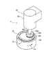
図6乃至図9に示す樹脂被膜の被覆装置4は、スピンナーテーブル機構5と、該スピンナーテーブル機構5を包囲して配設されたスピンナーテーブル収容手段6を具備している。スピンナーテーブル機構5は、スピンナーテーブル51と、該スピンナーテーブル51を回転駆動する電動モータ52と、該電動モータ52を上下方向に移動可能に支持する支持機構53を具備している。スピンナーテーブル51は多孔性材料から形成された吸着チャック511を具備しており、この吸着チャック511が図示しない吸引手段に連通されている。従って、スピンナーテーブル51は、吸着チャック511に被加工物であるウエーハを載置し図示しない吸引手段により負圧を作用せしめることにより吸着チャック51上にウエーハを保持する。電動モータ52は、その駆動軸521の上端に上記スピンナーテーブル51を連結する。上記支持機構53は、複数本(図示の実施形態においては3本)の支持脚531と、該支持脚531をそれぞれ連結し電動モータ52に取り付けられた複数本(図示の実施形態においては3本)のエアシリンダ532とからなっている。このように構成された支持機構53は、エアシリンダ532を作動することにより、電動モータ52およびスピンナーテーブル51を上方の位置である図7に示す被加工物搬入・搬出位置と、下方位置である図8に示す液状樹脂供給位置と、該液状樹脂供給位置より僅かに上方の図9に示す液状樹脂吸引位置に位置付ける。
Next, as described above, the resin film is formed on the back surface of the
The resin coating apparatus 4 shown in FIGS. 6 to 9 includes a
上記スピンナーテーブル収容手段6は、収容容器61と、該収容容器61を支持する3本(図6には2本が示されている)の支持脚62と、上記電動モータ52の駆動軸521に装着されたカバー部材63とを具備している。収容容器61は、図7乃至図9に示すように円筒状の外側壁611と底壁612と内側壁613とからなっている。底壁612の中央部には上記電動モータ52の駆動軸521が挿通する穴612aが設けられおり、この穴612aの周縁から上方に突出する内側壁613が形成されている。上記カバー部材63は、円盤状に形成されており、その外周縁から下方に突出するカバー部631を備えている。このように構成されたカバー部材63は、電動モータ52およびスピンナーテーブル51が図8に示す液状樹脂供給位置および図9に示す液状樹脂吸引位置に位置付けられると、カバー部631が上記収容容器61を構成する内側壁613の外側に隙間をもって重合するように位置付けられる。
The spinner table accommodating means 6 includes an
図示の樹脂被膜の被覆装置4は、上記スピンナーテーブル51に保持された半導体ウエーハ10の裏面中央領域(円形状の凹部104bの中央領域)に液状樹脂を供給する樹脂液供給手段7を具備している。樹脂液供給手段7は、スピンナーテーブル51に保持された半導体ウエーハ10の上面(円形状の凹部104bの上面)に向けて液状樹脂を供給する樹脂液供給ノズル71と、該樹脂液供給ノズル71を揺動せしめる正転・逆転可能な電動モータ72を備えており、樹脂液供給ノズル71が図示しない樹脂液供給源に接続されている。樹脂液供給ノズル71は、水平に延び先端部が下方に屈曲されたノズル部711と、該ノズル部711の基端から下方に延びる支持部712とからなっており、支持部712が上記収容容器61を構成する底壁612に設けられた図示しない挿通穴を挿通して配設され図示しない液状樹脂液供給源に接続されている。また、上記樹脂液供給ノズル71の支持部712が挿通する図示しない挿通穴の周縁には、支持部712との間をシールするシール部材(図示せず)が装着されている。
The illustrated resin film coating apparatus 4 includes a resin liquid supply means 7 for supplying a liquid resin to the central area of the back surface of the
図示の樹脂被膜の被覆装置4は、上記スピンナーテーブル51に保持された半導体ウエーハ10に供給され外周部に移動された液状樹脂の余剰分を吸引除去する液状樹脂吸引手段8を具備している。液状樹脂吸引手段8は、スピンナーテーブル51に保持された半導体ウエーハ10に供給され外周部に移動された液状樹脂の余剰分を吸引除去する吸引ノズル81と、該吸引ノズル81を揺動せしめる正転・逆転可能な電動モータ82を備えており、吸引ノズル81が図示しない吸引手段に接続されている。吸引ノズル81は、水平に延び先端部が下方に屈曲されたノズル部811と、該ノズル部811の基端から下方に延びる支持部812とからなっており、支持部812が上記収容容器61を構成する底壁612に設けられた図示しない挿通穴を挿通して配設され図示しない吸引手段に接続されている。なお、吸引ノズル81のノズル部811は、その先端は上記樹脂液供給ノズル71のノズル部711の先端より僅かに下方に伸びている。また、上記吸引ノズル81の支持部812が挿通する図示しない挿通穴の周縁には、支持部812との間をシールするシール部材(図示せず)が装着されている。
The resin coating apparatus 4 shown in the figure includes a liquid resin suction means 8 for sucking and removing excess liquid resin that has been supplied to the
図示の樹脂被膜の被覆装置4は以上のように構成されており、以下その作用について説明する。
上述したようにデバイス領域104に対応する裏面に円形状の凹部104bが形成され外周余剰領域105に対応する領域が残存されて環状の補強部105bが形成され半導体ウエーハ10は、図示しない搬送手段によってスピンナーテーブル51の吸着チャック511上に裏面を上側にして搬送され、該吸着チャック511に保護部材11側が吸引保持される(ウエーハ保持工程)。このとき、スピンナーテーブル51は図7に示す被加工物搬入搬出位置に位置付けられており、樹脂液供給ノズル71および吸引ノズル81は図6および図7に示すようにスピンナーテーブル51の上方から離隔した待機位置に位置付けられている。
The illustrated resin film coating apparatus 4 is configured as described above, and its operation will be described below.
As described above, the
半導体ウエーハ10をスピンナーテーブル51上に保持するウエーハ保持工程を実施したならば、スピンナーテーブル51上に保持された半導体ウエーハ10の裏面に形成された円形状の凹部104bの上面に樹脂被膜を被覆する樹脂被膜被覆工程を実施する。この樹脂被膜被覆工程は、先ずエアシリンダ532を作動してスピンナーテーブル51を図8に示す液状樹脂供給位置に位置付け、樹脂液供給手段7の電動モータ72を作動して液状樹脂供給ノズル71を支持部712を中心として揺動し、ノズル部711の先端をスピンナーテーブル51上に保持された半導体ウエーハ10の裏面に形成された円形状の凹部104bの中央領域の上方に位置付ける。
When the wafer holding step for holding the
次に、スピンナーテーブル機構5の電動モータ52を作動してスピンナーテーブル51を1000〜3000rpmの回転速度で回転する。従って、スピンナーテーブル51に保持された半導体ウエーハ10は、図10において矢印51aで示す方向に回転せしめられる。このように半導体ウエーハ10が回転している状態で、図10に示すように樹脂液供給手段7を作動して樹脂液供給ノズル71のノズル部711から半導体ウエーハ10の裏面に形成された円形状の凹部104bの中央領域に液状樹脂100を30秒間程度滴下する。この結果、半導体ウエーハ10の裏面に形成された円形状の凹部104bの中央領域に供給された液状樹脂100は、図11に示すように遠心力によって外周部まで流動し円形状の凹部104bの上面を被覆するとともに、円形状の凹部104bの滞留する。
Next, the
次に、樹脂液供給手段7の電動モータ72を作動して樹脂液供給ノズル71を図6および図7に示す待機位置に位置付ける。そして、液状樹脂吸引手段8の電動モータ82を作動して吸引ノズル81を支持部812を中心として揺動し、図9および図12に示すようにノズル部811の先端をスピンナーテーブル51に保持された半導体ウエーハ10の裏面に形成された円形状の凹部104bの隅部に位置付けるとともに、エアシリンダ532を作動してスピンナーテーブル51を液状樹脂吸引位置に位置付ける。また、スピンナーテーブル機構5の電動モータ52を回転速度を調整してスピンナーテーブル51を10rpm程度の回転速度で回転する。この結果、半導体ウエーハ10の裏面に形成された円形状の凹部104bの隅部に滞留する液状樹脂100の余剰分は、吸引ノズル81のノズル部811から吸引除去される。上述した樹脂被膜被覆工程を実施することにより、半導体ウエーハ10の裏面に形成された円形状の凹部104bの上面には、図13に示すように均一な厚さの樹脂被膜110が形成される。
Next, the
上述したように樹脂被膜被覆工程においては、半導体ウエーハ10の裏面に形成された円形状の凹部104bの中央領域に供給され遠心力によって外周部まで流動し円形状の凹部104bの隅部に滞留する液状樹脂100の余剰分は、吸引ノズル81のノズル部811から吸引除去されるので、生産性の良いスピンナーコーティングによって半導体ウエーハ10の裏面に形成された円形状の凹部104bの上面に均一な厚さの樹脂被膜110を形成することができる。
As described above, in the resin film coating step, the resin is supplied to the central region of the
2:研削装置
21:研削装置のチャックテーブル
22:研削手段
223:研削ホイール
225:研削砥石
4:樹脂被膜の被覆装置
5:スピンナーテーブル機構
51:スピンナーテーブル
52:電動モータ
53:支持機構
6:スピンナーテーブル収容手段
61:収容容器
7:樹脂液供給手段
71:樹脂液供給ノズル
8:液状樹脂吸引手段
81:吸引ノズル
10:半導体ウエーハ
101:ストリート
102:デバイス
104:デバイス領域
105:余剰領域
104b:円形状の凹部
105b:環状の補強部
100:液状樹脂
110:樹脂被膜
2: Grinding device 21: Chuck table 22 of grinding device: Grinding means 223: Grinding wheel 225: Grinding wheel 4: Resin film coating device 5: Spinner table mechanism 51: Spinner table 52: Electric motor 53: Support mechanism 6: Spinner Table storage means 61: Storage container 7: Resin liquid supply means 71: Resin liquid supply nozzle 8: Liquid resin suction means 81: Suction nozzle 10: Semiconductor wafer 101: Street 102: Device 104: Device area 105:
Claims (1)
ウエーハをスピンナーテーブルに裏面を上側にして保持するウエーハ保持工程と、
該スピンナーテーブルを回転しつつ該スピンナーテーブルに保持されたウエーハの裏面中央領域に液状樹脂を供給するとともに、ウエーハの裏面に供給された液状樹脂を遠心力によって外周に向けて流動させ、その後該凹部の隅部に滞留した液状樹脂を吸引除去する樹脂被膜被覆工程と、を含む、
ことを特徴とする樹脂被膜の被覆方法。 A device region in which a plurality of devices are formed on the front surface and an outer peripheral surplus region surrounding the device region, a thin concave portion is formed on the back surface corresponding to the device region, and an annular reinforcing portion is provided on the outer peripheral portion A method for coating a resin film on a back surface of a wafer, the method comprising:
A wafer holding step for holding the wafer on the spinner table with the back side facing up,
While rotating the spinner table, the liquid resin is supplied to the central region of the back surface of the wafer held by the spinner table, and the liquid resin supplied to the back surface of the wafer is caused to flow toward the outer periphery by centrifugal force, and then the concave portion Including a resin film coating step of sucking and removing the liquid resin staying in the corners of
A method for coating a resin film.
Priority Applications (1)
| Application Number | Priority Date | Filing Date | Title |
|---|---|---|---|
| JP2006097512A JP5000915B2 (en) | 2006-03-31 | 2006-03-31 | Resin coating method and coating apparatus |
Applications Claiming Priority (1)
| Application Number | Priority Date | Filing Date | Title |
|---|---|---|---|
| JP2006097512A JP5000915B2 (en) | 2006-03-31 | 2006-03-31 | Resin coating method and coating apparatus |
Publications (2)
| Publication Number | Publication Date |
|---|---|
| JP2007268422A JP2007268422A (en) | 2007-10-18 |
| JP5000915B2 true JP5000915B2 (en) | 2012-08-15 |
Family
ID=38671771
Family Applications (1)
| Application Number | Title | Priority Date | Filing Date |
|---|---|---|---|
| JP2006097512A Active JP5000915B2 (en) | 2006-03-31 | 2006-03-31 | Resin coating method and coating apparatus |
Country Status (1)
| Country | Link |
|---|---|
| JP (1) | JP5000915B2 (en) |
Families Citing this family (1)
| Publication number | Priority date | Publication date | Assignee | Title |
|---|---|---|---|---|
| JP5009254B2 (en) * | 2008-08-14 | 2012-08-22 | 株式会社ディスコ | Resin coating equipment |
Family Cites Families (6)
| Publication number | Priority date | Publication date | Assignee | Title |
|---|---|---|---|---|
| JPH0741534B2 (en) * | 1986-11-10 | 1995-05-10 | 不二越機械工業株式会社 | Wafer polishing method and polishing apparatus |
| JPS6478735A (en) * | 1987-09-17 | 1989-03-24 | Sanyo Electric Co | Substrate sticking method |
| JP2002197738A (en) * | 2000-12-28 | 2002-07-12 | Horon:Kk | Method and apparatus for applying adhesive on disk |
| JP4185704B2 (en) * | 2002-05-15 | 2008-11-26 | 株式会社ルネサステクノロジ | Manufacturing method of semiconductor device |
| JP2005317715A (en) * | 2004-04-28 | 2005-11-10 | Toshiba Corp | Method for manufacturing semiconductor integrated circuit |
| JP2006043623A (en) * | 2004-08-06 | 2006-02-16 | Seiko Epson Corp | Method for forming pattern, method for manufacturing device, device, method for manufacturing active matrix substrate, electro-optical device and electronic equipment |
-
2006
- 2006-03-31 JP JP2006097512A patent/JP5000915B2/en active Active
Also Published As
| Publication number | Publication date |
|---|---|
| JP2007268422A (en) | 2007-10-18 |
Similar Documents
| Publication | Publication Date | Title |
|---|---|---|
| JP4634949B2 (en) | Wafer holding pad | |
| JP5138325B2 (en) | Wafer processing method | |
| TWI534877B (en) | Protective film coating method and protective film covering device | |
| TW202022939A (en) | Substrate processing system andsubstrate processing method | |
| JP2010207723A (en) | Resin film forming apparatus | |
| JP7187112B2 (en) | Carrier plate removal method | |
| JP6791579B2 (en) | Wafers and wafer processing methods | |
| JP2017152442A (en) | Processing method | |
| JP2008006379A (en) | Protection film formation method | |
| JP6071702B2 (en) | Wafer processing method | |
| JP2010016146A (en) | Chuck table of processing apparatus | |
| JP2011108746A (en) | Method for processing wafer | |
| JP2007103582A (en) | Processing method and grinding apparatus of wafer | |
| JP5658586B2 (en) | Grinding equipment | |
| JP2011054808A (en) | Method of processing wafer, and wafer processed by the same | |
| JP4666583B2 (en) | Protective coating method | |
| JP5686570B2 (en) | How to use wafer support plate | |
| JP6999322B2 (en) | Wafer grinding method | |
| JP2012079910A (en) | Processing method of plate-like object | |
| JP5000915B2 (en) | Resin coating method and coating apparatus | |
| JP5306928B2 (en) | Wafer transfer device | |
| JP2007221030A (en) | Processing method for substrate | |
| JP2011071288A (en) | Method of processing wafer | |
| JP2011071287A (en) | Method of processing wafer | |
| JP2011071289A (en) | Method of processing wafer |
Legal Events
| Date | Code | Title | Description |
|---|---|---|---|
| A621 | Written request for application examination |
Free format text: JAPANESE INTERMEDIATE CODE: A621 Effective date: 20090203 |
|
| A977 | Report on retrieval |
Free format text: JAPANESE INTERMEDIATE CODE: A971007 Effective date: 20110330 |
|
| A131 | Notification of reasons for refusal |
Free format text: JAPANESE INTERMEDIATE CODE: A131 Effective date: 20110506 |
|
| A521 | Request for written amendment filed |
Free format text: JAPANESE INTERMEDIATE CODE: A523 Effective date: 20110704 |
|
| TRDD | Decision of grant or rejection written | ||
| A01 | Written decision to grant a patent or to grant a registration (utility model) |
Free format text: JAPANESE INTERMEDIATE CODE: A01 Effective date: 20120501 |
|
| A01 | Written decision to grant a patent or to grant a registration (utility model) |
Free format text: JAPANESE INTERMEDIATE CODE: A01 |
|
| A61 | First payment of annual fees (during grant procedure) |
Free format text: JAPANESE INTERMEDIATE CODE: A61 Effective date: 20120517 |
|
| R150 | Certificate of patent or registration of utility model |
Free format text: JAPANESE INTERMEDIATE CODE: R150 Ref document number: 5000915 Country of ref document: JP Free format text: JAPANESE INTERMEDIATE CODE: R150 |
|
| FPAY | Renewal fee payment (event date is renewal date of database) |
Free format text: PAYMENT UNTIL: 20150525 Year of fee payment: 3 |
|
| FPAY | Renewal fee payment (event date is renewal date of database) |
Free format text: PAYMENT UNTIL: 20150525 Year of fee payment: 3 |
|
| R250 | Receipt of annual fees |
Free format text: JAPANESE INTERMEDIATE CODE: R250 |
|
| R250 | Receipt of annual fees |
Free format text: JAPANESE INTERMEDIATE CODE: R250 |
|
| R250 | Receipt of annual fees |
Free format text: JAPANESE INTERMEDIATE CODE: R250 |
|
| R250 | Receipt of annual fees |
Free format text: JAPANESE INTERMEDIATE CODE: R250 |
|
| R250 | Receipt of annual fees |
Free format text: JAPANESE INTERMEDIATE CODE: R250 |
|
| R250 | Receipt of annual fees |
Free format text: JAPANESE INTERMEDIATE CODE: R250 |
|
| R250 | Receipt of annual fees |
Free format text: JAPANESE INTERMEDIATE CODE: R250 |
|
| R250 | Receipt of annual fees |
Free format text: JAPANESE INTERMEDIATE CODE: R250 |
|
| R250 | Receipt of annual fees |
Free format text: JAPANESE INTERMEDIATE CODE: R250 |
|
| R250 | Receipt of annual fees |
Free format text: JAPANESE INTERMEDIATE CODE: R250 |