JP4987142B2 - Game machine - Google Patents
Game machine Download PDFInfo
- Publication number
- JP4987142B2 JP4987142B2 JP2011107746A JP2011107746A JP4987142B2 JP 4987142 B2 JP4987142 B2 JP 4987142B2 JP 2011107746 A JP2011107746 A JP 2011107746A JP 2011107746 A JP2011107746 A JP 2011107746A JP 4987142 B2 JP4987142 B2 JP 4987142B2
- Authority
- JP
- Japan
- Prior art keywords
- voltage
- power supply
- circuit
- abnormality
- main control
- Prior art date
- Legal status (The legal status is an assumption and is not a legal conclusion. Google has not performed a legal analysis and makes no representation as to the accuracy of the status listed.)
- Expired - Fee Related
Links
Images


Description
本発明は、遊技ホールの営業終了後などに、万一、遊技機が違法改造されても、その事実を素早く検出できて違法遊技を未然に防止できる遊技機に関する。 The present invention relates to a gaming machine that can quickly detect the fact that the gaming machine is illegally modified after the game hall is closed and prevent illegal gaming.
パチンコ機などの弾球遊技機は、遊技盤に設けた図柄始動口と、複数の表示図柄による一連の図柄変動態様を表示する図柄表示部と、開閉板が開閉される大入賞口などを備えて構成されている。そして、図柄始動口に設けられた検出スイッチが遊技球の通過を検出すると入賞状態となり、遊技球が賞球として払出された後、図柄表示部では表示図柄が所定時間変動される。その後、7−7−7などの所定の態様で図柄が停止すると大当り状態となり、大入賞口が繰返し開放されて、遊技者に有利な利益状態を発生させている。但し、実際には、遊技球の入賞に基づく大当り抽選処理によって、大当り状態か否かが予め決定されており、図柄表示部では、専ら遊技者を盛上げるために図柄変動動作を行っている。 A ball game machine such as a pachinko machine has a symbol start opening provided on the game board, a symbol display section for displaying a series of symbol variation patterns by a plurality of display symbols, and a big winning opening for opening and closing the opening and closing plate. Configured. When the detection switch provided at the symbol start port detects the passage of the game ball, the winning state is entered, and after the game ball is paid out as a prize ball, the display symbol is changed for a predetermined time in the symbol display section. Thereafter, when the symbol is stopped in a predetermined manner such as 7-7-7, a big hit state is established, and the big winning opening is repeatedly opened to generate a profit state advantageous to the player. However, in actuality, whether or not the big hit state is determined in advance by the big hit lottery process based on the winning of the game ball, and the symbol display section performs the symbol changing operation exclusively to increase the player.
通常、この種の遊技機は、遊技動作を全体統括的に制御する主制御基板と、主制御基板から受ける制御コマンドに基づいて個別的な制御動作を実行するサブ制御基板とで構成されている。そして、主制御基板のコンピュータ回路は、前記した大当り抽選処理を含む制御プログラムに基づいて動作している。したがって、この制御プログラムを変更すれば、任意に大当り状態を招来させることも可能となり、そのような違法行為も報告されているところである。 Usually, this type of gaming machine is composed of a main control board for overall control of gaming operations and a sub control board for executing individual control operations based on control commands received from the main control board. . The computer circuit of the main control board operates based on a control program including the big hit lottery process. Therefore, if this control program is changed, it is possible to arbitrarily invite a big hit state, and such illegal acts have been reported.
具体的な違法行為としては、例えば、遊技ホールの営業終了後などに、遊技機の主制御基板を違法改造品と交換することが行われる。そこで、かかる違法行為に対処するべく各種の対策が採られている(例えば、特許文献1)。 As a specific illegal act, for example, after the game hall is closed, the main control board of the gaming machine is replaced with an illegally modified product. Therefore, various measures are taken to deal with such illegal acts (for example, Patent Document 1).
特許文献1に記載の発明では、制御基板の背面に、発光素子と受光素子とを有する反射型のフォトセンサを配置し、そのセンサを作動させるためのバッテリを電源基板とは別に設けている。
In the invention described in
しかしながら、上記の構成では、制御基板とフォトセンサとの隙間に、発光素子からのセンシング光を反射させる部材を挿入すれば、何の問題もなく制御基板を交換できることになる。また、フォトセンサやバッテリを設ける場所を、別に確保する必要があり、抜本的な機器構成の変更を要し、しかも、遊技機の組立工程も複雑化する。 However, in the above configuration, if a member that reflects sensing light from the light emitting element is inserted into the gap between the control board and the photosensor, the control board can be replaced without any problem. In addition, it is necessary to secure a place where a photo sensor and a battery are provided separately, which requires drastic changes in the device configuration, and also complicates the assembly process of the gaming machine.
本発明は、上記の問題点に鑑みてなされたものであって、防犯用の追加部材を必要とせず、必要最小限の回路変更だけで、違法改造行為を検出できる遊技機を提供することを目的とする。 The present invention has been made in view of the above problems, and provides a gaming machine that does not require an additional member for crime prevention and can detect an illegal remodeling action with only a necessary minimum circuit change. Objective.
上記の目的を達成するため、本発明は、遊技者に有利な遊技状態を発生させるか否かの抽選処理を実行して、その抽選結果に基づいて遊技動作を中心統括的に制御する主制御部と、前記主制御部からの指令に基づいて、個別的な制御動作を実行するサブ制御部と、外部から受けた交流電圧に基づいて生成された定常直流電圧と、前記交流電圧が遮断された後も所定期間は所定レベルを維持するバックアップ直流電圧とを、前記主制御部、及び/又は、前記サブ制御部に供給する電源部と、を有して構成され、前記電源部には、前記交流電圧を前記定常直流電圧に変換する変換回路と、前記バックアップ直流電圧の電圧異常又は電流異常を検出する異常検出回路と、前記異常検出回路の検出信号を受ける中間回路と、が設けられ、前記中間回路は、前記定常直流電圧を電源電圧として機能し、これが正常レベルを維持する限りON動作して前記異常検出回路の検出信号を他の回路に伝送しないよう構成されている。なお、遊技機としては、弾球遊技機の他に回胴遊技機が典型的である。
To achieve the above object, the present invention executes a lottery process for determining whether or not a game state advantageous to a player is generated, and controls the game operation centrally based on the lottery result. And a sub-control unit that executes individual control operations based on a command from the main control unit, a steady DC voltage generated based on an AC voltage received from the outside, and the AC voltage are cut off. And a power supply unit that supplies a backup DC voltage that maintains a predetermined level for a predetermined period to the main control unit and / or the sub control unit. A conversion circuit that converts the AC voltage into the steady DC voltage, an abnormality detection circuit that detects a voltage abnormality or current abnormality of the backup DC voltage, and an intermediate circuit that receives a detection signal of the abnormality detection circuit are provided, Intermediate circuit , The steady state DC voltage and functions as a power supply voltage, which is configured so as not to transmit to other circuits the detection signal of the abnormality detection circuit and turned ON so long as to maintain a normal level. In addition to the ball and ball game machines, the spinning machine is typical as the game machine.
上記した通り、本発明によれば、防犯用の追加部材を必要とせず、必要最小限の回路変更だけで、違法改造行為を検出できる遊技機を実現できる。 As described above, according to the present invention, it is possible to realize a gaming machine that can detect an illegal remodeling action with only a necessary minimum circuit change without requiring an additional member for crime prevention.
以下、本発明の実施形態について詳細に説明する。図1は、本実施形態のパチンコ機GMを示す斜視図である。このパチンコ機GMは、島構造体に着脱可能に装着される矩形枠状の木製外枠1と、外枠1に固着されたヒンジ2を介して開閉可能に枢着される前枠3とで構成されている。この前枠3には、遊技盤5が、裏側からではなく、表側から着脱自在に装着され、その前側には、ガラス扉6と前面板7とが夫々開閉自在に枢着されている。
Hereinafter, embodiments of the present invention will be described in detail. FIG. 1 is a perspective view showing a pachinko machine GM of the present embodiment. This pachinko machine GM includes a rectangular frame-shaped wooden
ガラス扉6の外周には、LEDランプなどによる電飾ランプが、略C字状に配置されている。前面板7には発射用の遊技球を貯留する上皿8が装着され、前枠3の下部には、上皿8から溢れ出し又は抜き取った遊技球を貯留する下皿9と、発射ハンドル10(HD)とが設けられている。発射ハンドル10は発射モータと連動しており、発射ハンドル10の回動角度に応じて動作する打撃槌によって遊技球が発射される。
On the outer periphery of the glass door 6, an electric lamp such as an LED lamp is arranged in a substantially C shape. An upper plate 8 for storing game balls for launch is mounted on the
上皿8の外周面には、チャンスボタン11が設けられている。このチャンスボタン11は、遊技者の左手で操作できる位置に設けられており、遊技者は、発射ハンドル10から右手を離すことなくチャンスボタン11を操作できる。このチャンスボタン11は、通常時には機能していないが、ゲーム状態がボタンチャンス状態となると内蔵ランプが点灯されて操作可能となる。なお、ボタンチャンス状態は、必要に応じて設けられるゲーム状態である。
A chance button 11 is provided on the outer peripheral surface of the upper plate 8. The chance button 11 is provided at a position where it can be operated with the left hand of the player, and the player can operate the chance button 11 without releasing the right hand from the
上皿8の右部には、カード式球貸し機に対する球貸し操作用の操作パネル12が設けられ、カード残額を3桁の数字で表示する度数表示部と、所定金額分の遊技球の球貸しを指示する球貸しスイッチと、ゲーム終了時にカードの返却を指令する返却スイッチとが設けられている。
On the right side of the upper plate 8, an
図2に示すように、遊技盤5には、金属製の外レールと内レールとからなるガイドレール13が環状に設けられ、その内側の遊技領域5aの略中央には、液晶カラーディスプレイDISPが配置されている。また、遊技領域5aの適所には、図柄始動口15、大入賞口16、複数個の普通入賞口17(大入賞口16の左右に4つ)、2つの通過口であるゲート18が配設されている。これらの入賞口15〜18は、それぞれ内部に検出スイッチを有しており、遊技球の通過を検出できるようになっている。
As shown in FIG. 2, the
液晶ディスプレイDISPは、大当り状態に係わる特定図柄を変動表示すると共に背景画像や各種のキャラクタなどをアニメーション的に表示する装置である。この液晶ディスプレイDISPは、中央部に特別図柄表示部Da〜Dcと右上部に普通図柄表示部19を有している。そして、特別図柄表示部Da〜Dcでは、大当り状態の招来を期待させるリーチ演出が実行されたり、特別図柄表示部Da〜Dc及びその周りでは、当否結果を不確定に報知する予告演出などが実行される。 The liquid crystal display DISP is a device that variably displays a specific symbol related to a big hit state and displays a background image and various characters in an animated manner. This liquid crystal display DISP has special symbol display portions Da to Dc in the center portion and a normal symbol display portion 19 in the upper right portion. And, in the special symbol display parts Da to Dc, a reach effect is executed that expects a big hit state to be invited, or in the special symbol display parts Da to Dc and the surroundings, a notice effect that informs the result of the success / failure is executed. Is done.
普通図柄表示部19は普通図柄を表示するものであり、ゲート18を通過した遊技球が
検出されると、普通図柄が所定時間だけ変動し、遊技球のゲート18の通過時点において抽出された抽選用乱数値により決定される停止図柄を表示して停止するようになっている。
The normal symbol display unit 19 displays a normal symbol. When a game ball that has passed through the
図柄始動口15は、左右1対の開閉爪15aを備えた電動式チューリップで開閉される
よう例えば構成され、普通図柄表示部19の変動後の停止図柄が当り図柄を表示した場合には、開閉爪15aが所定時間だけ、若しくは、所定個数の遊技球を検出するまで開放されるようになっている。
For example, the
図柄始動口15に遊技球が入賞すると、特別図柄表示部Da〜Dcの表示図柄が所定時間だけ変動し、図柄始動口15への遊技球の入賞タイミングに応じた抽選結果に基づいて決定される停止図柄で停止する。なお、特別図柄表示部Da〜Dc及びその周りでは、一連の図柄演出の間に、予告演出が実行される場合がある。
When a game ball wins the symbol start
大入賞口16は、例えば前方に開放可能な開閉板16aで開閉制御されるが、特別図柄表示部Da〜Dcの図柄変動後の停止図柄が「777」などの大当り図柄のとき、「大当りゲーム」と称する特別遊技が開始され、開閉板16aが開放されるようになっている。
The big winning
大入賞口16の開閉板16aが開放された後、所定時間が経過し、又は所定数(例えば10個)の遊技球が入賞すると開閉板16aが閉じる。このような動作は、最大で例えば15回まで特別遊技が継続され、遊技者に有利な状態に制御される。なお、特別図柄表示部Da〜Dcの変動後の停止図柄が特別図柄のうちの特定図柄であった場合には、特別遊技の終了後のゲームが高確率状態となるという特典が付与される。
After the opening /
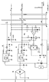
図3は、実施形態に係るパチンコ機の全体回路構成を示すブロック図である。図中の破線は、主に、直流電圧ラインを示している。 FIG. 3 is a block diagram showing an overall circuit configuration of the pachinko machine according to the embodiment. Broken lines in the figure mainly indicate DC voltage lines.
図示の通り、このパチンコ機は、AC24Vを受けて各種の直流電圧やシステムリセット信号(電源リセット信号)SYSやRAMクリア信号CLRなどを出力する電源基板20と、遊技制御動作を中心統括的に担う主制御基板21と、主制御基板21から受けた制御コマンドCMD’に基づいてランプ演出及び音声演出を実行する演出制御基板22と、演出制御基板22から受けた信号を各部に伝送する演出インタフェイス基板23と、演出インタフェイス基板23から受けた制御コマンドCMD”に基づいて液晶ディスプレイDISPを駆動する液晶制御基板24と、主制御基板21から受けた制御コマンドCMDに基づいて払出モータMを制御して遊技球を払い出す払出制御基板25と、遊技者による発射ハンドルHDの操作に応答して遊技球を発射させる発射制御基板26とを中心に構成されている。
As shown in the figure, this pachinko machine is centrally responsible for the game control operation and the
ここで、主制御基板21、演出制御基板22、液晶制御基板24、及び払出制御基板25には、ワンチップマイコンを備えるコンピュータ回路がそれぞれ搭載されている。そこで、主制御基板21、演出制御基板22、液晶制御基板24、及び払出制御基板25に搭載された回路、及びその回路によって実現される動作を機能的に総称して、本明細書では、主制御部21、演出制御部22、液晶制御部24、及び払出制御部25と言うことがある。又、主制御部21を除く全ての制御部又は一部の制御部を総称してサブ制御部と言う。
Here, the main control board 21, the
主制御部21は、払出制御部25に対して制御コマンドCMDを一方向に送信する一方、払出制御部25からは、遊技球の払出動作を示す賞球計数信号や、払出動作の異常に係わるステイタス信号CONを受信している。ステイタス信号CONには、例えば、補給切れ信号、払出不足エラー信号、下皿満杯信号が含まれる。 The main control unit 21 transmits a control command CMD in one direction to the payout control unit 25, while the payout control unit 25 relates to a prize ball count signal indicating a payout operation of game balls and an abnormality in the payout operation. The status signal CON is received. The status signal CON includes, for example, a replenishment signal, a payout shortage error signal, and a lower plate full signal.
図示の通り、主制御部21と払出制御部25には、電源基板20から、直流5Vのバックアップ電源BKが供給されている。したがって、営業終了や停電により交流電源24Vが遮断された後も、ワンチップマイコン内部のRAMのデータは保持される。
As shown in the figure, a backup power supply BK of
また、電源基板20は、交流電源24Vの遮断時に、主制御部21及び払出制御部25に、電圧降下信号ABNを出力するよう構成されている。そして、主制御部21及び払出制御部25では、フラグセンス方式によって、電圧降下信号ABNのレベル降下を把握した後、必要なデータをRAMに退避している。そのため、上記したバックアップ電源BKの作用とあいまって、主制御部21と払出制御部25では、営業開始時や停電からの復旧時に、電源遮断前の動作を再開できることになる。尚、主制御部21にのみバックアップ機能を持たせる、即ち、バックアップ電源BKや電圧降下信号ABNを主制御部21のみに供給する構成としてもよい。
Further, the
更にまた、電源基板20は、主制御部21と払出制御部25に対して、係員のスイッチ操作を示すRAMクリア信号CLRを出力している。このスイッチ操作は、主に電源投入時に実行されるが、バックアップ電源BKによって保持されているRAMの記憶内容を消去させるための操作である。したがって、各制御基板21,25では、RAMクリア信号CLRのレベルを判定することによって、係員によるスイッチ操作の有無を把握できることになる。尚、主制御部21にのみバックアップ機能を持たせた場合、RAMクリア信号CLRは主制御部21にのみ供給する。
Furthermore, the
図4は、電源基板20の電源回路を示す回路図である。実施形態の電源回路は、24Vの交流電圧を受ける交流入力部41と、交流入力部41が出力する交流電圧を脈流に変換する整流部42と、脈流電圧を平滑化する平滑回路43と、脈流電圧を受けて各種の直流電圧を出力する直流電源部44〜46と、主制御基板21から受ける帰還電圧RETに基づいて直流電源部44の動作を禁止する電源監視部PRHと、バックアップ電源を生成する蓄電部47と、過大な交流電圧を受けると、交流電源ラインLacを遮断状態にする交流遮断部48と、交流入力部41が出力する交流電圧を整流する直流生成回路49と、過大な交流電圧を受けるとON動作して直流生成回路49の出力電圧を降下させるレベル監視部50と、直流生成回路49の出力電圧レベルに応じてON/OFF動作する直流遮断部51と、電源リセット信号SYSと電圧降下信号ABNを生成する電源監視回路52とで構成されている。なお、電源リセット信号は、システムリセット信号SYSに他ならない。
FIG. 4 is a circuit diagram showing a power supply circuit of the
交流入力部41は、電源入力ラインPWの一方を溶断させる溶断ヒューズFu1と、電源入力ラインPW,PWを両断する電源スイッチSWと、機器内部のノイズが外部に漏出することを防止するラインフィルタ(L1,C1〜C3,R1)と、遊技球などの静電気を放電する帯電防止部(Sa,VR1〜VR3)とで構成されている。ラインフィルタは、各電源入力ラインPW,PWに、直列接続される一対のコイルL1と、一対のコイルL1の両端を接続する一対のコンデンサC1と、各電源入力ラインPW,PWとアース間に接続されるコンデンサC2,C3と、電源入力ラインPW,PWの間に接続される抵抗R1とで構成されている。
The
帯電防止部は、遊技球を蓄える遊技球タンク(不図示)に設けられた導電板に接続されたサージアブソーバSaと、各電源入力ラインPW,PWの間に接続されたバリスタVR1と、各電源入力ラインPW,PWとアース間に接続されたバリスタVR2,VR3とで構成されている。なお、タンク導電板とサージアブソーバSaの接続点は、フレームグランドFGに接続されている。 The antistatic unit includes a surge absorber Sa connected to a conductive plate provided in a game ball tank (not shown) for storing game balls, a varistor VR1 connected between the power input lines PW and PW, and each power source. The varistors VR2 and VR3 are connected between the input lines PW and PW and the ground. The connection point between the tank conductive plate and the surge absorber Sa is connected to the frame ground FG.
整流部42は、ブリッジ型の3つの全波整流回路で構成されている。すなわち、ダイオードD1,D2,D3,D4で第1整流回路が構成され、ダイオードD1,D2,D5,D6で第2整流回路が構成され、ダイオードD1,D2,D7,D8で第3整流回路が構成されている。
The
平滑回路43は、第1整流回路が出力する脈流を平滑するコンデンサC4と、直流電源
ラインを溶断させる溶断ヒューズFu2とで構成されている。そして、平滑回路43から出力される+32Vの直流電圧は、主制御基板21などを経由してソレノイド類に供給される。なお、+32Vの直流電源ラインに過大な電流が流れると、溶断ヒューズFu2が溶断する。
The smoothing
直流電源部44は、平滑コンデンサC5と、降圧型のスイッチングレギュレータSR1とで構成され、+12Vの直流電圧を出力している。そして、+12Vの直流電圧は、主制御基板21、払出制御基板25、及び液晶制御基板24に供給されている。
The DC
直流電源部45は、平滑コンデンサC6と、降圧型のスイッチングレギュレータSR2とで構成され、+15Vの直流電圧を出力している。そして、+15Vの直流電圧は、演出インタフェイス基板23に搭載されたデジタルアンプだけに供給されている。
The DC
直流電源部46は、平滑コンデンサC6と、降圧型のスイッチングレギュレータSR3とで構成されて+5Vの直流電圧を出力している。そして、+5Vの直流電圧は、液晶制御基板24と演出インタフェイス基板23に供給されている。なお、主制御基板21と払出制御基板25で必要となるDC5Vの電圧については、各制御基板21,25で受けたDC12Vの電圧を降圧させて生成している。
The DC
蓄電部47は、ダイオードD9とコンデンサC7とで構成されている。この+5Vの直流電圧は、主制御部21と払出制御部25のワンチップマイコンの内蔵RAMのデータを保持するバックアップ電源となる。
The
交流遮断部48は、交流24Vの交流電源ラインLac1,Lac2に接続された2つのダイオードD13,D14と、ダイオードD13,D14の接続点に接続されたツェナーダイオードZD2及び抵抗R7の直列回路と、ダイオードD13,D14の上流側において、一方側の交流電源ラインLac1に直列接続された溶断ヒューズFu3と、ダイオードD13,D14の下流側において、一方側の交流電源ラインLac1に直列接続された溶断ヒューズFu4とで構成されている。
The
2つのダイオードD13,D14は、交流電源ラインLac1,Lac2から交流電流が侵入しないよう、何れのダイオードD13,D14も、電流の侵入を阻止する方向に直列接続されている。また、ツェナーダイオードZD2は、他方側の交流電源ラインLac2から、ダイオードD13,D14の接続点に向けて、降伏電流が流れる向きに接続されている。 The two diodes D13 and D14 are connected in series in a direction that prevents the intrusion of current so that an alternating current does not enter from the AC power supply lines Lac1 and Lac2. The Zener diode ZD2 is connected in a direction in which a breakdown current flows from the AC power supply line Lac2 on the other side toward the connection point of the diodes D13 and D14.
ツェナーダイオードZD2は、通常は、OFF状態であるが、交流電源ラインLac1,Lac2に過大な交流電圧(例えばAC100V)が加わると、降伏状態となる。この降伏状態では、交流電源ラインLac2→抵抗R7→ツェナーダイオードZD2→ダイオードD13→交流電源ラインLac1の経路で、ツェナーダイオードZD2の降伏電流が流れるので、溶断ヒューズFu3が溶断される。なお、抵抗R7は、ツェナーダイオードZD2やダイオードD13の破損を防止する保護抵抗である。 The Zener diode ZD2 is normally in an OFF state, but when an excessive AC voltage (for example, AC 100V) is applied to the AC power supply lines Lac1 and Lac2, the Zener diode ZD2 enters a breakdown state. In this breakdown state, since the breakdown current of the Zener diode ZD2 flows through the path of the AC power supply line Lac2, the resistor R7, the Zener diode ZD2, the diode D13, and the AC power supply line Lac1, the fusing fuse Fu3 is blown. The resistor R7 is a protective resistor that prevents the Zener diode ZD2 and the diode D13 from being damaged.
直流生成回路49は、2つの交流電源ラインLac1,Lac2と、フレームグランド
FGとの間に設けられた両波整流回路である。そして、2つの交流電源ラインLac1,Lac2の間に直列接続された2つのダイオードD10,D11と、電流制限抵抗R4と、平滑コンデンサC9と、抵抗R5,R6が直列接続された負荷抵抗とで構成されている。2つのダイオードD10,D11は、各アノード端子が交流電源ラインLac1,Lac2に接続される一方、各カソード端子は、電流制限抵抗R4と、ツェナーダイオードZD1に共通して接続されている。なお、抵抗R4は、レベル監視部50に対する電流制限抵抗であり、また、直列接続された抵抗R5,R6は、スイッチング動作するパワートランジスタQ2のバイアス抵抗でもある。
The DC generation circuit 49 is a double-wave rectification circuit provided between two AC power supply lines Lac1 and Lac2 and the frame ground FG. Then, two diodes D10 and D11 connected in series between the two AC power supply lines Lac1 and Lac2, a current limiting resistor R4, a smoothing capacitor C9, and a load resistor in which resistors R5 and R6 are connected in series. Has been. The two diodes D10 and D11 have their anode terminals connected to the AC power supply lines Lac1 and Lac2, while the cathode terminals are commonly connected to the current limiting resistor R4 and the Zener diode ZD1. The resistor R4 is a current limiting resistor for the
直流生成回路49は、上記の通りに構成されるので、平滑コンデンサC9は、交流電源ラインLac1,Lac2の交流電圧の波高値に近い値まで充電される。また、負荷抵抗として機能する抵抗R5,R6の両端電圧は、平滑された直流電圧となる。 Since the DC generation circuit 49 is configured as described above, the smoothing capacitor C9 is charged to a value close to the peak value of the AC voltage of the AC power supply lines Lac1 and Lac2. The voltage across the resistors R5 and R6 that function as load resistors is a smoothed DC voltage.
レベル監視部50は、バイアス回路(R2,R3,C8)と、スイッチングトランジスタQ1とで構成されて、交流電源ラインLac1,Lac2の何れかが異常レベルでないかを監視している。そして、2つのダイオードD10,D11と、ツェナーダイオードZD1と、バイアス抵抗R2,R3とが、交流電源ラインLac1,Lac2とフレームグランドFGとの間に直列接続されている。ダイオードD10,D11の接続点には、ツェナーダイオードZD1が、ダイオードD10,D11とは逆向きに、つまり、電流を阻止する方向に直列接続されている。
The
また、直列接続されたバイアス抵抗R2,R3の両端には、コンデンサC8が並列接続されている。そして、直列接続されたバイアス抵抗R2,R3の接続点に、トランジスタQ1のベース端子が接続されている。また、トランジスタQ1のコレクタ端子は、電流制限抵抗R4と平滑コンデンサC9の接続点に接続され、トランジスタQ1のエミッタ端子は、フレームグランドFGに接続されている。 Further, a capacitor C8 is connected in parallel to both ends of the bias resistors R2 and R3 connected in series. The base terminal of the transistor Q1 is connected to a connection point between the bias resistors R2 and R3 connected in series. The collector terminal of the transistor Q1 is connected to the connection point between the current limiting resistor R4 and the smoothing capacitor C9, and the emitter terminal of the transistor Q1 is connected to the frame ground FG.
一方、直流遮断部51は、大電流容量のパワートランジスタQ2と、平滑コンデンサC9に並列接続された抵抗R5,R6とで構成されている。2つの抵抗R5,R6は直列接続されており、その接続点は、パワートトランジスタQ2のベース端子に接続されている。なお、抵抗R6は、パワートトランジスタQ2のベース端子とエミッタ端子との間に接続されている。これら2つの抵抗R5,R6は、パワートトランジスタQ2のバイアス抵抗として機能する。またパワートランジスタQ2のコレクタ端子はグランドに接続され、エミッタ端子は、フレームグランドFGに接続されている。 On the other hand, the DC cut-off unit 51 includes a power transistor Q2 having a large current capacity and resistors R5 and R6 connected in parallel to the smoothing capacitor C9. The two resistors R5 and R6 are connected in series, and the connection point is connected to the base terminal of the powered transistor Q2. The resistor R6 is connected between the base terminal and the emitter terminal of the powered transistor Q2. These two resistors R5 and R6 function as a bias resistor for the powered transistor Q2. The collector terminal of the power transistor Q2 is connected to the ground, and the emitter terminal is connected to the frame ground FG.
正常状態では、直流生成回路49の平滑コンデンサC9の両端には、所定レベルの直流電圧が発生している。そのため、パワートランジスタQ2は、ベース端子に十分な正電圧を受けることでON状態となり、コレクタ端子とエミッタ端子間は導通状態となる。したがって、フレームグランドFGとアース間も導通状態である。 In a normal state, a predetermined level of DC voltage is generated across the smoothing capacitor C9 of the DC generation circuit 49. For this reason, the power transistor Q2 is turned on by receiving a sufficient positive voltage at the base terminal, and the collector terminal and the emitter terminal are brought into conduction. Therefore, the frame ground FG and the ground are also conductive.
トランジスタQ2のコレクタ端子とエミッタ端子は、整流部42と平滑回路43など接続する位置に配置されており、トランジスタQ2はON状態であることを条件に、平滑回路43や直流電源部44〜46などが機能することになる。
The collector terminal and the emitter terminal of the transistor Q2 are arranged at a position where the rectifying
ここで、交流電源ラインLac1,Lac2の何れかと、フレームグランドFGとの電位差が、ツェナーダイオードZD1の降伏電圧を超える異常時を想定する。かかる異常時には、ダイオードD10又はダイオードD11→ツェナーダイオードZD1→バイアス抵抗R2,R3の向きに電流が流れ、トランジスタQ1のベース電位を上昇させる。そのため、トランジスタQ1は、OFF状態からON状態に遷移して、平滑コンデンサC9の両端電圧を急激に降下させる。 Here, it is assumed that the potential difference between one of the AC power supply lines Lac1 and Lac2 and the frame ground FG exceeds the breakdown voltage of the Zener diode ZD1. At the time of such an abnormality, current flows in the direction of the diode D10 or the diode D11 → the Zener diode ZD1 → the bias resistors R2 and R3, and raises the base potential of the transistor Q1. Therefore, the transistor Q1 transitions from the OFF state to the ON state, and the voltage across the smoothing capacitor C9 is suddenly dropped.
すると、パワートランジスタQ2のベース電位も降下するので、パワートランジスタQ2がON状態からOFF状態に遷移することになる。そして、パワートランジスタQ2が開放状態となって、平滑回路43や直流電源部44〜46への給電が停止されて、各回路が非動作状態となる。
Then, since the base potential of the power transistor Q2 also drops, the power transistor Q2 changes from the ON state to the OFF state. And power transistor Q2 will be in an open state, power supply to smoothing
実施形態の電源回路では、4つの溶断ヒューズFu1〜Fu4に加えて、交流遮断部48と、直流遮断部51とを特徴的に備えている。したがって、AC24Vの交流電源ラインに、誤って交流100Vを加えてしまう場合でも、ICやその他の電子素子の破損が有効に防止される。すなわち、AC100Vの過大電圧は、バイアス抵抗R2,R3を経由してトランジスタQ1をON動作させるので、直ちに、トランジスタQ2がOFF状態となり、アースラインが切断されて、直流電源部44〜46を保護すると共に、直流電源の供給を受ける各制御基板上のICや電子素子を保護する。しかも、交流電圧が正常値に戻ると、トランジスタQ2もON状態に復帰し、電源回路は正常な動作を再開する。
In the power supply circuit of the embodiment, in addition to the four blow fuses Fu1 to Fu4, an
図5は、図4の一部を詳細に図示したものであり、整流部42と、+5Vの電源電圧を生成する直流電源部46と、電源遮断後も所定の電圧レベル(+5V)を維持する蓄電部47と、+12Vの電源電圧を生成する直流電源部44と、直流電源部44(スイッチングレギュレータSR1)の出力側の異常を監視する電源監視部PRHとを具体的に図示している。
FIG. 5 shows a part of FIG. 4 in detail, and maintains a predetermined voltage level (+5 V) even after the power is cut off, and the rectifying
図示の通り、電源基板20と主制御基板21とは、電源基板20のコネクタCN1と、主制御基板21のコネクタCN2とを経由して接続されている。そして、直流5Vのバックアップ電源BKと、直流12Vと、RAMクリア信号CLRとが、不図示の電源リセット信号SYS及び電圧降下信号ABNと共に、電源基板20から主制御基板21に供給されている。
As illustrated, the
RAMクリア信号CLRは、電源基板20に接続されたRAMクリアスイッチSWと、主制御基板21に搭載された電流制限抵抗r1と、主制御基板21の電源回路で12Vから5Vに降圧された電源電圧5Vとで生成される。そして、RAMクリアスイッチSWがON操作された状態では、RAMクリア信号CLRがLレベルとなる。
The RAM clear signal CLR includes a RAM clear switch SW connected to the
電源基板20から主制御部21に供給されたバックアップ電源BKは、ワンチップマイコンのRAMに供給されるが、このバックアップ電源BKは、帰還電圧RETとして、そのまま電源基板20に戻される。図示の通り、この回路例では、帰還電圧RETは、電流制限抵抗r2を通して、フォトカプラPHのフォトダイオードに供給されている。
The backup power supply BK supplied from the
電源監視部PRHは、帰還電圧RETが正常か否かを判定する判定回路(異常検出回路)CR1と、判定回路CR1の出力を受ける中間回路CR2と、判定回路CR1の出力を受けて直流電源部44の動作を禁止する動作禁止回路CR3とで構成されている。ここで、中間回路CR2の電源電圧は、直流電源部44が出力する直流電圧12Vである。一方、判定回路CR1と動作禁止回路CR3は、バックアップ電源BKを受けて動作している。したがって、判定回路CR1と動作禁止回路CR3は、遊技ホールの営業が終了して、電源が遮断された後も、引き続き機能することになる。
The power supply monitoring unit PRH has a determination circuit (abnormality detection circuit) CR1 that determines whether or not the feedback voltage RET is normal, an intermediate circuit CR2 that receives the output of the determination circuit CR1, and a DC power supply unit that receives the output of the determination circuit CR1. And an operation prohibiting circuit CR3 for prohibiting the operation of 44. Here, the power supply voltage of the intermediate circuit CR <b> 2 is a
判定回路CR1は、具体的には、フォトカプラPHで構成され、フォトカプラPHのフォトダイオードとフォトトランジスタには、電流制限抵抗r2,r3と、逆方向電流阻止用のダイオードDsとが接続されている。 Specifically, the determination circuit CR1 includes a photocoupler PH, and current limiting resistors r2 and r3 and a reverse current blocking diode Ds are connected to the photodiode and the phototransistor of the photocoupler PH. Yes.
中間回路CR2は、短絡トランジスタQ5と、ベース抵抗r8と、コレクタ抵抗r7と
、逆方向電流阻止用のダイオードDsとでスイッチング回路を構成している。中間回路は、直流電源部44が出力する直流電圧12Vで機能するので、電源が投入されて、遊技機が正常に動作を開始した後は、短絡トランジスタQ5は、必ずON状態となる。そのため、遊技動作中、ノイズなどの影響で、仮に、検出トランジスタQ4がON状態からOFF状態に変化しても、検出トランジスタQ4の出力電圧の立ち上がりが、D型フリップフロップ60に伝達されることはない。
In the intermediate circuit CR2, a short circuit transistor Q5, a base resistor r8, a collector resistor r7, and a reverse current blocking diode Ds constitute a switching circuit. Since the intermediate circuit functions with a DC voltage of 12 V output from the DC
動作禁止回路CR3は、ラッチ回路たるD型フリップフロップ60で構成されている。D型フリップフロップ60は、例えば、汎用デジタルICたるSN7474で構成される。このSN7474は、D入力端子と、クロック端子CLKと、Q出力端子と、クリア端子CLRとを有しており、クロック端子CLKの信号がHレベルに立ち上がると、その時のD入力端子の入力電圧をQ出力端子に出力し、その後はその状態を維持する。一方、クリア端子CLRにLレベルの信号を受けると、Q出力端子はLレベルとなる。
The operation prohibiting circuit CR3 includes a D-type flip-
図5の回路構成では、D型フリップフロップ60のD入力端子には、Hレベルの電圧が固定的に供給されている。一方、クロック端子CLKは、フォトカプラPHのフォトトランジスタのコレクタ端子に接続されている。そのため、D型フリップフロップ60のクロック端子CLKへの入力信号、つまり、フォトカプラPHの出力信号がHレベルに立ち上がると、D型フリップフロップ60のQ出力端子はHレベルとなり、その後は、その状態を維持する。
In the circuit configuration of FIG. 5, an H level voltage is fixedly supplied to the D input terminal of the D flip-
一方、D型フリップフロップ60のクリア端子CLRには、RAMクリア信号CLRが供給されている。したがって、係員によってRAMクリアスイッチSWがON操作されると、D型フリップフロップ60のQ出力端子はLレベルとなり、その後、フォトカプラPHの出力信号がHレベルに立ち上がらない限り、その状態を維持する。
On the other hand, the RAM clear signal CLR is supplied to the clear terminal CLR of the D-type flip-
スイッチングレギュレータSR1,SR3は、例えば、降圧チョッパ方式の電源ICで構成され、ここでは、図5(b)に等価回路を示すLM2576が使用される。なお、回路図を簡略化するため、出力電圧が固定タイプのIC(LM2576)を使用し、フィードバック(Feedback)経路に分圧抵抗R1,R2を外付けすることなく、各々+12Vと+5Vとを生成している。また、簡易化の観点から、図5(a)には、チョークコイルL01,L02と、フライホールダイオードD01,D02と、出力コンデンサCoだけを図示している。 The switching regulators SR1 and SR3 are configured by, for example, a step-down chopper type power supply IC, and here, an LM2576 whose equivalent circuit is shown in FIG. 5B is used. In order to simplify the circuit diagram, a fixed output type IC (LM2576) is used, and + 12V and + 5V are generated without externally attaching voltage dividing resistors R1 and R2 to the feedback path, respectively. is doing. Further, from the viewpoint of simplification, FIG. 5A shows only the choke coils L01 and L02, the flyhole diodes D01 and D02, and the output capacitor Co.
ところで、スイッチングレギュレータSR1,SR3(LM2576)は、外部シャットダウン機能を有している。そして、そのON/OFF入力端子にHレベルの電圧を供給すると、スイッチングレギュレータは、スタンバイ状態となり、その後、ON/OFF入力端子にLレベルの電圧を受けるまで、機能を停止するようになっている。 Incidentally, the switching regulators SR1, SR3 (LM2576) have an external shutdown function. When an H level voltage is supplied to the ON / OFF input terminal, the switching regulator enters a standby state, and then stops functioning until an L level voltage is received at the ON / OFF input terminal. .
そこで、この実施形態では、スイッチングレギュレータSR1については、動作禁止回路たるD型フリップフロップ60からの信号に基づいて、その外部シャットダウン機能を発揮させている。すなわち、D型フリップフロップ60のQ出力を、スイッチングレギュレータSR1のON/OFF入力端子に供給して、HレベルのQ出力によって、シャットダウン機能を発揮させて直流電源部44の動作を禁止している。
Therefore, in this embodiment, the switching regulator SR1 exhibits its external shutdown function based on a signal from the D-type flip-
以下、この動作禁止動作について、違法行為に即して説明する。例えば、違法行為者が遊技機を違法改造する場合は、遊技機の電源が遮断された遊技ホールの営業終了後であると思われる。そのような時間帯には、交流入力電圧(AC24V)が途絶えているので、直流電源部44,46はともに機能していない。したがって、中間回路CR2はOFF状態を維持し、他の回路に影響を与えない。
Hereinafter, this operation prohibiting operation will be described in accordance with illegal acts. For example, when an illegal actor illegally modifies a gaming machine, it seems that it is after the game hall where the power of the gaming machine is cut off is closed. In such a time zone, the AC input voltage (
一方、バックアップ電源BKは機能しているので、これを電源電圧とする判定回路CR1と動作禁止回路CR3については、主制御部21のRAMと共に有効に機能している。 On the other hand, since the backup power supply BK is functioning, the determination circuit CR1 and the operation prohibition circuit CR3 using this as the power supply voltage function effectively together with the RAM of the main control unit 21.
このような状態で、違法行為者が主制御基板21を交換する場合には、少なくとも、正規の主制御基板21を、コネクタCN2から取り外す必要がある。なお、正規の主制御基板21は、基板ケースに厳重に封印されているので、違法行為者は、基板ケースごと主制御基板を交換すると思われる。何れにしても、コネクタCN2が主制御基板21から外されたことによって、それまでフォトカプラPHに供給されていた帰還電圧RETが途絶え、フォトトランジスタの電流も途絶えることになり、フォトカプラの出力電圧は、LレベルからHレベルに立ち上がる。 In this state, when an illegal person replaces the main control board 21, it is necessary to remove at least the regular main control board 21 from the connector CN2. It should be noted that the legitimate main control board 21 is strictly sealed in the board case, so that the illegal person seems to replace the main control board with the board case. In any case, when the connector CN2 is disconnected from the main control board 21, the feedback voltage RET previously supplied to the photocoupler PH is interrupted, the current of the phototransistor is also interrupted, and the output voltage of the photocoupler Rises from L level to H level.
この変化は、D型フリップフロップ60のクロック端子CLKに伝わるので、その結果、D型フリップフロップ60のQ出力がHレベルに立ち上がる。なお、その後、違法な主制御基板21の接続によって、仮に、帰還電圧RETが正常値に復帰したとしても、D型フリップフロップ60のクロック端子CLKがLレベルの立ち下がるだけであり、HレベルのQ出力は維持される。また、違法作業時のチャタリングなどによって、繰り返しクロック端子CLKのレベルが変化したとしても、D型フリップフロップ60のQ出力はHレベルを維持する。
This change is transmitted to the clock terminal CLK of the D-type flip-
このようにして違法改造された遊技機は、その状態のまま翌日の営業開始時を迎える。そして、営業開始に先立って、交流電圧が遊技機に供給されるので、直流電源部45と直流電源部46については、スイッチングレギュレータとしての動作を開始する。しかし、直流電源部44については、そのスイッチングレギュレータSR1のON/OFF端子が、Hレベルに維持されているので、シャットダウン機能が発揮されて、スタンバイ状態のままとなり、+12Vを出力しない。したがって、主制御基板21は動作を開始することができず、この異常事態によって違法行為の事実が判明することになる。なお、万一、電源監視部PRHが誤動作したような場合には、RAMクリアスイッチSWを押すと、D型フリップフロップ60のQ出力がLレベルに戻るので、直流電源部44の動作を開始されることができる。
The gaming machine illegally modified in this way reaches the start of business the next day in that state. Since the AC voltage is supplied to the gaming machine prior to the start of business, the DC
以上の通り、図5の回路構成によれば、違法改造された遊技機が遊技動作を開始することがないので、違法遊技を確実に未然防止することができる。なお、正常の動作を開始した遊技機についても、遊技動作中、常に、帰還電圧RETを受けることになるが、本実施例では、ON動作状態の中間回路CR2が、判定回路CR1の出力を短絡させるので、配線ケーブルに重畳するノイズなどが全く問題にならない。 As described above, according to the circuit configuration of FIG. 5, an illegally modified gaming machine does not start a gaming operation, so that illegal gaming can be surely prevented. Note that the gaming machine that has started normal operation always receives the feedback voltage RET during the game operation. In this embodiment, the intermediate circuit CR2 in the ON operation state short-circuits the output of the determination circuit CR1. Therefore, noise superimposed on the wiring cable is not a problem at all.
以上、LM2576を使用する回路図について説明したが、使用するICが変われば、電源監視部PRHの回路構成が変更されるのは当然である。図6(a)は、LM2586を使用した回路例であり、LM2586の等価回路(図6(b))も含めて図示している。この回路では、分圧抵抗R1,R2を外付けして、その抵抗比によって+12Vの出力電圧を設定している。また、D型フリップフロップ60のQバー出力が、NOTゲートGを経由して、LM2586のON/OFF入力端子に供給される。なお、この回路構成では、プルアップ抵抗r4と、アイソレーションダイオードDaと、スイッチング周波数を規定する調整抵抗raとが必要となるが、その他の回路構成は、図5の場合と同じである。
The circuit diagram using the LM2576 has been described above, but it is natural that the circuit configuration of the power supply monitoring unit PRH is changed when the IC used is changed. FIG. 6A is a circuit example using the LM2586, and includes an equivalent circuit of the LM2586 (FIG. 6B). In this circuit, voltage dividing resistors R1 and R2 are externally attached, and an output voltage of +12 V is set according to the resistance ratio. Further, the Q bar output of the D-type flip-
ところで、図5や図6の回路構成では、交流電圧が遮断された後は、バックアップ電源BKからフォトダイオード及びフォトトランジスタに、継続して電流が流れることになり、コンデンサC7の充電電荷が放電し切ってしまうおそれがある。そこで、そのような場
合には、コンデンサC7に代えて、バックアップ電源BKのための充電電池を配置するのが好ましい。
By the way, in the circuit configurations of FIGS. 5 and 6, after the AC voltage is cut off, current continuously flows from the backup power source BK to the photodiode and the phototransistor, and the charge of the capacitor C7 is discharged. There is a risk of cutting. Therefore, in such a case, it is preferable to arrange a rechargeable battery for the backup power source BK instead of the capacitor C7.
また、フォトカプラPHでの消費電流が問題になる場合には、図5や図6の回路構成に代えて、図7の回路構成を採るべきである。図7の電源監視部PRHは、帰還電圧RETの検出トランジスタQ4と、検出トランジスタQ4のコレクタ電圧を短絡させる短絡トランジスタQ5と、D型フリップフロップ60とで構成されている。
Further, when the current consumption in the photocoupler PH becomes a problem, the circuit configuration of FIG. 7 should be adopted instead of the circuit configuration of FIG. 5 or FIG. 7 includes a detection transistor Q4 for the feedback voltage RET, a short-circuit transistor Q5 for short-circuiting the collector voltage of the detection transistor Q4, and a D-type flip-
そして、検出トランジスタQ4と、ベース抵抗r5と、コレクタ抵抗r6と、電流の逆流を防止するダイオードDsとで、帰還電圧RETが正常か否かを判定する判定回路を構成している。この判定回路は、バックアップ電源BKに基づいて動作しており、検出トランジスタQ4は、正常時には、常にON状態となっている。しかし、この回路構成では、ベース抵抗r5やコレクタ抵抗r6の抵抗値を十分大きく設定することによって、検出トランジスタQ4のON電流を十分小さく抑制することができる。 The detection transistor Q4, the base resistor r5, the collector resistor r6, and the diode Ds that prevents the reverse current flow constitute a determination circuit that determines whether or not the feedback voltage RET is normal. This determination circuit operates based on the backup power supply BK, and the detection transistor Q4 is always in the ON state when it is normal. However, in this circuit configuration, the ON current of the detection transistor Q4 can be sufficiently reduced by setting the resistance values of the base resistor r5 and the collector resistor r6 to be sufficiently large.
ところで、短絡トランジスタQ5と、ベース抵抗r8と、コレクタ抵抗r7と、電流の逆流を防止するダイオードDsとで、もう一つのスイッチング回路(中間回路)を構成している。そして、遊技機が正常に動作を開始した後は、短絡トランジスタQ5は、必ずON状態となる。そのため、遊技動作中、ノイズなどの影響で、仮に、検出トランジスタQ4がON状態からOFF状態に変化しても、検出トランジスタQ4の出力電圧の立ち上がりが、D型フリップフロップ60に伝達されることはない。
Incidentally, the short-circuit transistor Q5, the base resistor r8, the collector resistor r7, and the diode Ds for preventing the backflow of current constitute another switching circuit (intermediate circuit). Then, after the gaming machine starts operating normally, the short-circuit transistor Q5 is always turned on. Therefore, during the game operation, even if the detection transistor Q4 changes from the ON state to the OFF state due to the influence of noise, the rise of the output voltage of the detection transistor Q4 is transmitted to the D-type flip-
一方、遊技ホールの営業が終了して交流入力電圧が遮断された後は、短絡トランジスタQ5の電源電圧が消滅する。そのため、短絡トランジスタQ5がON状態になることはなく、検出トランジスタQ4の出力電圧が、そのまま、D型フリップフロップ60に伝達されることになる。
On the other hand, after the game hall is closed and the AC input voltage is cut off, the power supply voltage of the short-circuit transistor Q5 disappears. Therefore, the short-circuit transistor Q5 is not turned on, and the output voltage of the detection transistor Q4 is transmitted to the D-type flip-
このような遊技ホールの営業終了後、もし、主制御基板21を交換しようとして、正規の主制御基板21をコネクタCN2から取り外すと、検出トランジスタQ4がOFF動作する。そして、検出トランジスタQ4のコレクタ電圧の立ち上がりが、そのまま、D型フリップフロップ60のクロック端子CLKに伝達されるので、スイッチングレギュレータSR1のON/OFF入力端子がHレベルとなる。そして、このHレベルは、翌日の営業開始までを維持されるので、遊技機への電源投入後は、スイッチングレギュレータSR1がスタンバイ状態となって+12Vを出力しない。したがって、主制御基板21は動作を開始することができず、この事態によって違法行為の事実が判明することになる。
After the game hall is closed, if the main control board 21 is removed from the connector CN2 in order to replace the main control board 21, the detection transistor Q4 is turned off. Since the rise of the collector voltage of the detection transistor Q4 is directly transmitted to the clock terminal CLK of the D-type flip-
以上、違法改造時には、正規の主制御基板21を、基板ケースごとコネクタCN2から取り外されるであろうと想定した。しかし、主制御基板21の基板ケースに穴を開けて、ワンチップマイコンだけを交換することも考えられる。このような違法行為は、その痕跡が基板ケースに残るので、発生可能性が低いものの、やはり対策は必要である。 As described above, it is assumed that the legitimate main control board 21 will be removed from the connector CN2 together with the board case at the time of illegal modification. However, it is also conceivable to make a hole in the board case of the main control board 21 and replace only the one-chip microcomputer. Such an illegal act remains in the substrate case, so the possibility of occurrence is low, but measures are still necessary.
そこで、正規の主制御基板21が、基板ケースごとコネクタCN2から外されたか否かに拘らず、違法行為を検出するためには、図8の回路構成が採用される。図8の電源監視部PRHは、バックアップ電源BKの電圧上昇を検出するコンパレータQ6と、コンパレータQ6の出力を短絡させる短絡トランジスタQ5と、D型フリップフロップ60と、異常報知回路61とで構成されている。なお、コンパレータQ6には、出力電流制限回路が内蔵されているので、その出力端子が短絡トランジスタQ5によって継続して短絡されても問題は生じない。
Therefore, regardless of whether or not the regular main control board 21 is removed from the connector CN2 together with the board case, the circuit configuration of FIG. 8 is adopted to detect illegal actions. The power supply monitoring unit PRH in FIG. 8 includes a comparator Q6 that detects a voltage increase of the backup power supply BK, a short-circuit transistor Q5 that short-circuits the output of the comparator Q6, a D-type flip-
この電源監視部PRHでは、主制御基板21がコネクタCN2から取り外されるか、或
いは、主制御基板21のワンチップマイコンがICソケットから取り外されると、バックアップ電源BKの電圧値が微妙に上昇することを利用している。そして、バックアップ電源BKとしては、十分な電流容量を確保するため、好ましくは、充電式の電池が使用される。また、この回路構成では、スイッチングレギュレータSR1のシャットダウン機能を使用しない。これは、図8の回路構成では、バックアップ電源BKの電圧上昇を判定するので、違法行為を誤認する可能性も否定し切れないからである。
In the power supply monitoring unit PRH, when the main control board 21 is removed from the connector CN2 or the one-chip microcomputer of the main control board 21 is removed from the IC socket, the voltage value of the backup power supply BK slightly increases. We are using. And as backup power supply BK, in order to ensure sufficient current capacity, a rechargeable battery is preferably used. In this circuit configuration, the shutdown function of the switching regulator SR1 is not used. This is because in the circuit configuration of FIG. 8, since the voltage increase of the backup power supply BK is determined, the possibility of misrecognizing illegal activities cannot be denied.
図示の通り、異常報知回路61は、D型フリップフロップ60のQ出力端子に接続されたダイオードDmと、ダイオードDmの出力電圧を受けるコンデンサCmと、コンデンサCmの両端電圧を受けるNOTゲートGmと、発光ダイオードDe及び報知ブザーBZなどで構成されている。
As illustrated, the
そして、D型フリップフロップ60のQ出力が、ダイオードDmを経由してコンデンサCmに供給され、異常レベルたるHレベルのQ出力が、コンデンサCmに記憶されるようになっている。また、コンデンサCmの両端電圧は、出力ドライバを兼ねたNOTゲートGmを経由して、異常信号ERRとして主制御基板21に伝送される。主制御基板21は、電源基板20から異常信号ERRを受信した場合、払出制御部25に対して払出しを禁止する旨の情報を送信するのが好ましい。又、発射動作を停止させるのも好適である。これらの禁止動作は、例えば、RAMクリア信号CLRを受信した場合に解除される。
The Q output of the D-type flip-
また、NOTゲートGmの出力がLレベルになると、発光ダイオードDeが異常点灯され報知ブザーBZが鳴るよう構成されている。但し、NOTゲートGmは、スイッチングレギュレータSR3が出力する電源電圧5Vを受けて動作しており、したがって、遊技機に電源が投入されるまでは機能しない。また、D型フリップフロップ60のクリア端子CLRには、RAMクリア信号CLRに代えて、電源リセット信号SYSが供給されている。そのため、遊技機に電源が投入されると、D型フリップフロップ60のQ出力端子は、必ずLレベルとなる。したがって、一々、RAMクリアスイッチSWを操作する必要はない。
Further, when the output of the NOT gate Gm becomes L level, the light emitting diode De is abnormally turned on and the notification buzzer BZ is sounded. However, the NOT gate Gm operates in response to the
この電源監視部PRHでは、異常検出回路として、バックアップ電源BKで動作するコンパレータQ6が配置されている。ここで、コンパレータQ6の非反転入力端子(+)には、バックアップ電源BKを分圧抵抗r10,r11で分圧した検出電圧Eiが供給される。一方、反転入力端子(−)には、ツェナーダイオードDZの基準電圧Erが供給される。なお、ツェナーダイオードDZは、電流制限抵抗r9を経由してバックアップ電源BKに接続されている。 In the power supply monitoring unit PRH, a comparator Q6 that operates with the backup power supply BK is disposed as an abnormality detection circuit. Here, the non-inverting input terminal (+) of the comparator Q6 is supplied with a detection voltage Ei obtained by dividing the backup power source BK with the voltage dividing resistors r10 and r11. On the other hand, the reference voltage Er of the Zener diode DZ is supplied to the inverting input terminal (−). Note that the Zener diode DZ is connected to the backup power source BK via the current limiting resistor r9.
基準電圧Erは、バックアップ電源BKが主制御基板21に給電されている正常時には、検出電圧Ei<基準電圧Erとなるよう設定されている。そのため、正常時には、コンパレータQ6の出力は常にLレベルであり、短絡トランジスタQ5のON/OFF状態に拘らず、D型フリップフロップ60のクロック入力端子CLKもLレベルとなる。
The reference voltage Er is set so that the detection voltage Ei <the reference voltage Er when the backup power supply BK is normally supplied to the main control board 21. Therefore, at the normal time, the output of the comparator Q6 is always at the L level, and the clock input terminal CLK of the D-type flip-
このような回路構成を有する遊技機において、交流入力電圧が遮断された後に、主制御基板21か、そのワンチップマイコンが交換された場合を考える。このような場合には、バックアップ電源BKからの給電が停止されるタイミングにおいて、バックアップ電源BKの電圧値が微妙に上昇する。すると、バックアップ電源BKの電圧値が増加した分だけ検出電圧Eiが増加して、検出電圧Ei>基準電圧Erとなる。その結果、コンパレータQ6の出力がLレベルからHレベルに変化するので、この変化を、クロック端子CLKに受けるD型フリップフロップ60は、そのQ出力がHレベルとなり、このHレベルがダイオードDmを経由してコンデンサCmに記憶される。なお、このタイミングでは、NOTゲートGmは、電源電圧を受けていないので機能しない。
Consider a case in which the main control board 21 or its one-chip microcomputer is replaced after the AC input voltage is cut off in the gaming machine having such a circuit configuration. In such a case, the voltage value of the backup power supply BK slightly increases at the timing when the power supply from the backup power supply BK is stopped. Then, the detection voltage Ei increases by the increase in the voltage value of the backup power supply BK, and the detection voltage Ei> the reference voltage Er. As a result, since the output of the comparator Q6 changes from L level to H level, the D-type flip-
その後、営業開始に先立って交流入力電圧が供給されると、電源リセット信号SYSによって、D型フリップフロップ60のQ出力はLレベルに戻される。しかし、ダイオードDmが存在するのでコンデンサCmの充電電圧が直ぐには降下しない。そして、コンデンサCmのHレベルの両端電圧は、動作を開始したNOTゲートを経由して、主制御基板21に異常信号ERRとして供給される。また、発光ダイオードDeが異常点灯するとともに、警報ブザーBZが鳴る。なお、コンデンサCmの充電電圧は、NOTゲートGmの動作開始と共に徐々に降下するが、数10秒程度は、Hレベルを維持するよう、大容量のコンデンサCmが使用されており、数10秒間は警報音が持続する。
Thereafter, when an AC input voltage is supplied prior to the start of business, the Q output of the D-type flip-
何れにしても、Lレベルの異常信号ERRを受けた主制御基板21では、異常事態の発生をホールコンピュータに通報するか、或いは、これに加えて警報表示をするなどの報知動作を実行することになる。この図8の回路構成によれば、如何なる場合にも、スイッチングレギュレータSR1をスタンバイモードにしないので、誤動作によって主制御基板21への給電が停止されるおそれが皆無である。また、図8の回路構成では、主制御基板21から電源基板20への帰還電圧RETが不要であるので、電源基板20に、全ての回路を収容することができ、したがって、違法行為者の対抗措置を極めて困難にしている。
In any case, the main control board 21 that has received the L level abnormality signal ERR notifies the hall computer of the occurrence of an abnormal situation, or in addition to this, performs a notification operation such as displaying an alarm. become. According to the circuit configuration of FIG. 8, since the switching regulator SR1 is not put into the standby mode in any case, there is no possibility that power supply to the main control board 21 is stopped due to malfunction. Further, in the circuit configuration of FIG. 8, since the feedback voltage RET from the main control board 21 to the
ところで、他の回路基板へ異常信号ERRを出力する異常報知回路61を設けると共に、如何なる場合にも、スイッチングレギュレータSR1をスタンバイモードに設定しない図8の回路構成は、図5、図6、図7の回路においても、好適に採用できるのは勿論である。この場合、D型フリップフロップ60のクリア端子CLRには、電源リセット信号SYSが供給されるのが好適である。
By the way, the
また、図8の回路構成では、バックアップ電源BKの電圧異常を検出する構成を採ったが、これに代えて、バックアップ電源BKの電源ラインの電流変化を検出する構成を採ることもできる。例えば、図9に示すように、電源ラインに設けた検出一次コイルLs1と、コンパレータの接続された検出二次コイルLs2とを密に電磁結合される構成が例示される。この回路構成では、バックアップ電源BKの電圧降下が問題にならないので充電電池は不要であり大容量のコンデンサC7で足りる。 Further, in the circuit configuration of FIG. 8, a configuration for detecting a voltage abnormality of the backup power source BK is adopted, but instead, a configuration for detecting a current change in the power source line of the backup power source BK may be employed. For example, as shown in FIG. 9, a configuration in which a detection primary coil Ls1 provided on a power supply line and a detection secondary coil Ls2 connected to a comparator are electromagnetically coupled closely is exemplified. In this circuit configuration, since the voltage drop of the backup power supply BK does not become a problem, a rechargeable battery is unnecessary and a large-capacitance capacitor C7 is sufficient.
そして、主制御基板がコネクタCN2から外されるか、ワンチップマイコンがソケットから外されると、電源ラインの電流が遮断されるので、その変化が検出コイルによって検出されてコンパレータQ6の出力が立ち上がる。そのため、D型フリップフロップ60のQ出力がHレベルとなり、異常事態の発生が翌日まで記憶保持される。
When the main control board is removed from the connector CN2 or the one-chip microcomputer is removed from the socket, the current of the power supply line is cut off, so that the change is detected by the detection coil and the output of the comparator Q6 rises. . Therefore, the Q output of the D-type flip-
以上、本発明の実施形態を具体的に説明したが、具体的な記載内容は何ら本発明を限定するものではなく、各種の改変が可能である。 As mentioned above, although embodiment of this invention was described concretely, the concrete description content does not limit this invention at all, and various modifications are possible.
例えば、図8〜図10に示す電源監視部PRHにおいて、D型フリップフロップ60のQ出力を、スイッチングレギュレータSR1のON/OFF入力端子に供給しても良い。但し、この場合には、D型フリップフロップ60のクリア端子CLRには、RAMクリア信号CLRが供給される。
For example, in the power supply monitoring unit PRH shown in FIGS. 8 to 10, the Q output of the D-type flip-
更にまた、スイッチングレギュレータSR1のシャットダウン機能を活用する図5〜図7の回路構成において、図8に示すような異常報知回路61を追加するのも好適である。このような場合、図10に示すように、D型フリップフロップ60のクリア端子CLRに、RAMクリア信号CLRを供給するのであれば、ダイオードDmやコンデンサCmは不要となる。なお、破線で示すように、スイッチングレギュレータSR1のシャットダウン機能を活用しても良い。
Furthermore, it is also preferable to add an
なお、上記の説明では、専ら主制御基板21の違法改造を問題にしたが、払出制御基板25についても違法改造が懸念される場合には、電源基板20と払出制御基板25との間に、前記した各回路と同様の回路構成が採用される。
In the above description, illegal modification of the main control board 21 has been a problem. However, if illegal modification of the payout control board 25 is concerned, the
GM 遊技機
20 電源基板
BK バックアップ直流電圧
21 主制御部
CR1 異常検出回路
CR3 動作禁止回路
Claims (8)
前記主制御部からの指令に基づいて、個別的な制御動作を実行するサブ制御部と、
外部から受けた交流電圧に基づいて生成された定常直流電圧と、前記交流電圧が遮断された後も所定期間は所定レベルを維持するバックアップ直流電圧とを、前記主制御部、及び/又は、前記サブ制御部に供給する電源部と、を有して構成され、
前記電源部には、前記交流電圧を前記定常直流電圧に変換する変換回路と、前記バックアップ直流電圧の電圧異常又は電流異常を検出する異常検出回路と、前記異常検出回路の検出信号を受ける中間回路と、が設けられ、
前記中間回路は、前記定常直流電圧を電源電圧として機能し、これが正常レベルを維持する限りON動作して前記異常検出回路の検出信号を他の回路に伝送しないよう構成されていることを特徴とする遊技機。 A main control unit that executes a lottery process for determining whether or not to generate a gaming state advantageous to the player, and centrally controls the game operation based on the lottery result;
Based on a command from the main control unit, a sub-control unit that executes individual control operations;
A stationary DC voltage generated based on an AC voltage received from the outside, and a backup DC voltage that maintains a predetermined level for a predetermined period after the AC voltage is cut off, the main control unit, and / or the A power supply unit that supplies power to the sub-control unit,
The power supply unit includes a conversion circuit that converts the AC voltage into the steady DC voltage, an abnormality detection circuit that detects a voltage abnormality or current abnormality of the backup DC voltage, and an intermediate circuit that receives a detection signal of the abnormality detection circuit And provided,
The intermediate circuit includes a wherein a constant DC voltage serves as a power supply voltage, which is configured not to transmit the detection signal of the abnormality detection circuit and turned ON so long as to maintain a normal level for other circuits To play.
Priority Applications (1)
| Application Number | Priority Date | Filing Date | Title |
|---|---|---|---|
| JP2011107746A JP4987142B2 (en) | 2011-05-13 | 2011-05-13 | Game machine |
Applications Claiming Priority (1)
| Application Number | Priority Date | Filing Date | Title |
|---|---|---|---|
| JP2011107746A JP4987142B2 (en) | 2011-05-13 | 2011-05-13 | Game machine |
Related Parent Applications (1)
| Application Number | Title | Priority Date | Filing Date |
|---|---|---|---|
| JP2008001823A Division JP4836964B2 (en) | 2008-01-09 | 2008-01-09 | Game machine |
Publications (2)
| Publication Number | Publication Date |
|---|---|
| JP2011147830A JP2011147830A (en) | 2011-08-04 |
| JP4987142B2 true JP4987142B2 (en) | 2012-07-25 |
Family
ID=44535344
Family Applications (1)
| Application Number | Title | Priority Date | Filing Date |
|---|---|---|---|
| JP2011107746A Expired - Fee Related JP4987142B2 (en) | 2011-05-13 | 2011-05-13 | Game machine |
Country Status (1)
| Country | Link |
|---|---|
| JP (1) | JP4987142B2 (en) |
Families Citing this family (1)
| Publication number | Priority date | Publication date | Assignee | Title |
|---|---|---|---|---|
| JP5509506B1 (en) * | 2012-12-14 | 2014-06-04 | 山佐株式会社 | Game machine |
Family Cites Families (3)
| Publication number | Priority date | Publication date | Assignee | Title |
|---|---|---|---|---|
| JP3859129B2 (en) * | 2001-12-17 | 2006-12-20 | 株式会社藤商事 | Game machine |
| JP2005137429A (en) * | 2003-11-04 | 2005-06-02 | Samii Kk | Game machine |
| JP4736409B2 (en) * | 2004-11-30 | 2011-07-27 | 株式会社三洋物産 | Game machine |
-
2011
- 2011-05-13 JP JP2011107746A patent/JP4987142B2/en not_active Expired - Fee Related
Also Published As
| Publication number | Publication date |
|---|---|
| JP2011147830A (en) | 2011-08-04 |
Similar Documents
| Publication | Publication Date | Title |
|---|---|---|
| JP4904211B2 (en) | Bullet ball machine | |
| JP4836964B2 (en) | Game machine | |
| US7683571B2 (en) | Electronic device, method for controlling the same, and program for the same | |
| JP2012143309A (en) | Game machine | |
| JP4611353B2 (en) | Game machine | |
| JP4819758B2 (en) | Game machine | |
| JP4987142B2 (en) | Game machine | |
| JP4726861B2 (en) | Game machine | |
| JP4714755B2 (en) | Game machine | |
| JP4714754B2 (en) | Game machine | |
| JP2010148814A (en) | Game machine | |
| JP4498321B2 (en) | Game machine | |
| JP2010012322A (en) | Game machine | |
| JP4987138B2 (en) | Game machine | |
| JP4726862B2 (en) | Game machine | |
| JP4836880B2 (en) | Bullet ball machine | |
| JP2009213672A (en) | Game machine | |
| JP2012143310A (en) | Game machine | |
| JP5239085B2 (en) | Game machine | |
| JP5695116B2 (en) | Game machine | |
| JP4452698B2 (en) | Game machine | |
| JP4806065B2 (en) | Game machine | |
| JP4478946B2 (en) | Game machine | |
| JP2001286613A (en) | Power source unit for game machine | |
| JP4806064B2 (en) | Game machine |
Legal Events
| Date | Code | Title | Description |
|---|---|---|---|
| A521 | Written amendment |
Free format text: JAPANESE INTERMEDIATE CODE: A523 Effective date: 20110513 |
|
| A621 | Written request for application examination |
Free format text: JAPANESE INTERMEDIATE CODE: A621 Effective date: 20110513 |
|
| TRDD | Decision of grant or rejection written | ||
| A01 | Written decision to grant a patent or to grant a registration (utility model) |
Free format text: JAPANESE INTERMEDIATE CODE: A01 Effective date: 20120403 |
|
| A01 | Written decision to grant a patent or to grant a registration (utility model) |
Free format text: JAPANESE INTERMEDIATE CODE: A01 |
|
| A61 | First payment of annual fees (during grant procedure) |
Free format text: JAPANESE INTERMEDIATE CODE: A61 Effective date: 20120424 |
|
| R150 | Certificate of patent or registration of utility model |
Free format text: JAPANESE INTERMEDIATE CODE: R150 Ref document number: 4987142 Country of ref document: JP Free format text: JAPANESE INTERMEDIATE CODE: R150 |
|
| FPAY | Renewal fee payment (event date is renewal date of database) |
Free format text: PAYMENT UNTIL: 20150511 Year of fee payment: 3 |
|
| R250 | Receipt of annual fees |
Free format text: JAPANESE INTERMEDIATE CODE: R250 |
|
| R250 | Receipt of annual fees |
Free format text: JAPANESE INTERMEDIATE CODE: R250 |
|
| R250 | Receipt of annual fees |
Free format text: JAPANESE INTERMEDIATE CODE: R250 |
|
| R250 | Receipt of annual fees |
Free format text: JAPANESE INTERMEDIATE CODE: R250 |
|
| R250 | Receipt of annual fees |
Free format text: JAPANESE INTERMEDIATE CODE: R250 |
|
| R250 | Receipt of annual fees |
Free format text: JAPANESE INTERMEDIATE CODE: R250 |
|
| LAPS | Cancellation because of no payment of annual fees |