JP4967209B2 - Manufacturing method of semiconductor device - Google Patents
Manufacturing method of semiconductor device Download PDFInfo
- Publication number
- JP4967209B2 JP4967209B2 JP2001260976A JP2001260976A JP4967209B2 JP 4967209 B2 JP4967209 B2 JP 4967209B2 JP 2001260976 A JP2001260976 A JP 2001260976A JP 2001260976 A JP2001260976 A JP 2001260976A JP 4967209 B2 JP4967209 B2 JP 4967209B2
- Authority
- JP
- Japan
- Prior art keywords
- layer
- buffer layer
- igbt
- collector
- thickness
- Prior art date
- Legal status (The legal status is an assumption and is not a legal conclusion. Google has not performed a legal analysis and makes no representation as to the accuracy of the status listed.)
- Expired - Lifetime
Links
Images


Description
【0001】
【発明の属する技術分野】
本発明は、半導体装置およびその製造方法に関し、特に絶縁ゲート型バイポーラトランジスタ(以下、IGBTとする)を構成する半導体装置およびその製造方法に関する。
【0002】
【従来の技術】
図7は、従来のプレナー構造のパンチスルー型IGBT(以下、PT−IGBTとする)を示す縦断面図である。図7に示すように、PT−IGBTは、n-ドリフト層11、n+バッファー層12およびp+コレクタ層13からなるエピタキシャルウェハ10の、n-ドリフト層11の表面にp+ベース領域14、n+エミッタ領域15、ゲート絶縁膜16、ゲート電極17およびエミッタ電極18が形成され、p+コレクタ層13の表面にコレクタ電極19が形成された構成となっている。PT−IGBTでは、オフ時にn-ドリフト層11内が完全に空乏化し、空乏層がn+バッファー層12まで到達する。
【0003】
縦型IGBTでは、オン電圧を低くするため、p+コレクタ層13の濃度を濃くしてできるだけ電気抵抗を小さくする必要がある。その結果、p+コレクタ層13からn-ドリフト層11内に注入されるキャリアが非常に多くなり、スイッチング損失およびスイッチング速度の著しい悪化を招く。そこで、ライフタイムキラーの導入により、デバイス特性を調整する必要がある。
【0004】
図8は、従来のプレナー構造のノンパンチスルー型IGBT(以下、NPT−IGBTとする)を示す縦断面図である。図8に示すように、NPT−IGBTは、n-ドリフト層21を構成するFZウェハの表面にp+ベース領域24、n+エミッタ領域25、ゲート絶縁膜26、ゲート電極27およびエミッタ電極28が形成され、FZウェハの裏面にp+コレクタ層23が低温拡散技術プロセスにより形成され、さらにコレクタ電極29が形成された構成となっている。NPT−IGBTでは、オフ時にn-ドリフト層21内が完全に空乏化せず、空乏層はp+コレクタ層23に到達しない。NPT−IGBTでは、ライフタイムキラーを導入せずに、p+コレクタ層23の濃度および厚さによりデバイス特性が調整される。
【0005】
近時、さらなる低損失化を図るため、PT−IGBTとNPT−IGBTのそれぞれの長所を兼ね備えるフィールドストップ型IGBT(以下、FS−IGBTとする)がLaskaらにより提案されている(ISPSD’00,P.355−358,(2000))。FS−IGBTは、n-ドリフト層、n+フィールドストップ層およびp+コレクタ層からなる。n+フィールドストップ層を設けることにより、必要な耐圧を得るためのn-ドリフト層を薄くすることができるので、オン電圧を低減させることができる。
【0006】
また、n+フィールドストップ層およびp+コレクタ層が非常に薄いので、IEEE’97,P.213−216(1997)の中でPorstらが言及しているTransparency Emitter効果により各層に蓄積しているキャリアが少ないので、スイッチング損失が抑えられる。また、FS−IGBTでは、NPT−IGBTと同様に、p+コレクタ層の濃度でデバイス特性が調整されるため、ライフタイムキラーは導入されない。
【0007】
上述したFS−IGBTまたはそれに類似したデバイスを作製する方法として、つぎの2つが知られている。第1の方法は、FZウェハを研磨して100〜120μm程度の厚さにした後に、イオン注入および熱拡散をおこなってn+フィールドストップ層およびp+コレクタ層を形成する方法である。第2の方法は、従来のn-ドリフト層、n+バッファー層およびp+コレクタ層を構成するエピタキシャルウェハを用い、p+コレクタ層を0.5μm程度の厚さとなるように研磨する方法である。この第2の方法では、n+バッファー層はPT−IGBTと同じである(Matsudaiら、ISPSD’01,P.441−444,(2001))。
【0008】
【発明が解決しようとする課題】
しかしながら、高温状態での漏れ電流の増加を抑制するためにはn+フィールドストップ層は厚いのが好ましいが、上述した第1の方法では、n+フィールドストップ層およびp+コレクタ層を厚く形成することができず、濃度が低くなってしまうので、良好な電気的特性が得られないという問題点がある。また、Transparency Emitter効果を得るためにはp+コレクタ層の厚さは1μm以下であるのが好ましいが、上述した第2の方法では、p+コレクタ層を研磨する際に実際には±3μm程度のばらつきが生じるので、削り代を考慮するとp+コレクタ層の厚さは3μm以上でなければならないという問題点がある。
【0009】
本発明は、上記問題点に鑑みてなされたものであって、電気的特性に優れたIGBTを構成する半導体装置を提供することを目的とする。また、本発明は、電気的特性に優れたIGBTを構成する半導体装置を安定して作製することが可能な半導体装置の製造方法を提供することを目的とする。
【0010】
【課題を解決するための手段】
上記目的を達成するため、本発明は、第1導電型のドリフト層の上にドリフト層よりも不純物濃度が高い第1導電型の第1のバッファー層がエピタキシャル成長され、さらに第1のバッファー層の上に第1のバッファー層よりも不純物濃度が低い第1導電型の第2のバッファー層がエピタキシャル成長されてなるエピタキシャルウェハを用いる。このエピタキシャルウェハの、ドリフト層側の面にベース部およびエミッタ部を形成する。また、エピタキシャルウェハの、第2のバッファー層側の面を所定のウェハ厚さになるまで研磨した後に、その研磨面にコレクタ部を形成する。
【0011】
この発明によれば、第2のバッファー層が研磨時のばらつきを吸収するバッファー層となり、ドリフト層の上面にベース部およびエミッタ部を有し、第1および第2のバッファー層を介して第2のバッファー層の下面にコレクタ部を有する半導体装置が得られる。
【0012】
【発明の実施の形態】
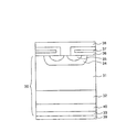
以下に、本発明の実施の形態について図面を参照しつつ詳細に説明する。図1は、本発明にかかる半導体装置を構成するプレナー型IGBTの構造の一例を示す縦断面図である。このIGBTは、n-ドリフト層31、第1のバッファー層であるn+バッファー層32、および第2のバッファー層であるn-バックグラインドバッファー層40からなるエピタキシャルウェハ30を用いて作製されている。このエピタキシャルウェハ30の、n-ドリフト層31の表面には、p+ベース領域34、n+エミッタ領域35、ゲート絶縁膜36、ゲート電極37およびエミッタ電極38が形成されている。エピタキシャルウェハ30の、n-バックグラインドバッファー層40の表面には、p+コレクタ層33およびコレクタ電極39が形成されている。
【0013】
以下に耐圧値に対するn-ドリフト層厚の関係を示す。
W=2Ksε0・Vce/qNd
ただし、W=n-ドリフト層厚、Vce=素子耐圧値、Ks=11.7、ε0=8.857×10¹⁴、q=1.602×10¹⁹である。
【0014】
したがって、n-ドリフト層31の厚さは0.1134×Vce[μm]以下であり、たとえば、1200V耐圧クラス素子(実際には1400Vの耐圧値が必要)に必要なn-ドリフト層31の厚は、W=0.1134・Vce=0.1134×1400=159[μm]となり、最低でも159[μm]以上は必要となる。
【0015】
また、n+バッファー層32の不純物濃度は1×1014cm-3以上で、かつ1×1016cm-3以下である。これは、n+バッファー層32の不純物濃度が1×1014cm-3以下であれば、n+バッファー層32で空乏層をストップできなくなり、耐圧低下を招いてしまうからである。一方、n+バッファー層32の不純物濃度が1×1016cm-3以上であれば、コレクタ層からの正孔の注入を妨げることになってしまい、これによってオン電圧の低下を招き、IGBT動作をしなくなってしまうからである。
【0016】
また、n+バッファー層32の厚さは10μm以下である。これは、n+バッファー層32があまり厚いと、スイッチング動作時(特にターンオフ時)にスイッチング損失の増加を招き、特性が悪くなるからである。したがって、スイッチング損失低減のためには、n+バッファー層32の厚みは10μm以下と薄い方が望ましい。
【0017】
また、n-バックグラインドバッファー層40の不純物濃度はn+バッファー層32の不純物濃度よりも低い。また、n-バックグラインドバッファー層40の厚さは10μm以下である。すなわち、このn-バックグラインドバッファー層40においても上記n+バッファー層32と同様に、スイッチング損失を低減するためには薄い方が望ましい。そして、バックグラインドの制御性から、この層の厚みは10μm以下が望ましい。
【0018】
また、p+コレクタ層33の不純物濃度はn+バッファー層32の平均不純物濃度の10倍以上である。すなわちIGBTのオン電圧を小さくするためには、コレクタ層の不純物濃度はn+バッファー層の不純物濃度の10倍以上が望ましい。また、p+コレクタ層33の厚さは1μm以下である。すなわち、上記Transparency Emitter効果によるスイッチング損失低減のためにはコレクタ層の厚みは1μm以下が望ましい。また、エピタキシャルウェハ30の初期厚さは200μm以上である。
【0019】
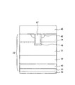
図1に示す構成のIGBTの製造プロセスについて図2〜図5を参照しながら説明する。まず、図2に示すように、n-ドリフト層31の上にn+バッファー層32をエピタキシャル成長し、さらにその上にn-バックグラインドバッファー層40をエピタキシャル成長してなるエピタキシャルウェハ30を用意する。そして、図3に示すように、このエピタキシャルウェハ30の、n-ドリフト層31の表面に、p+ベース領域34、n+エミッタ領域35、ゲート絶縁膜36、ゲート電極37およびエミッタ電極38を、フォトリソグラフィ技術、エッチングおよびイオン注入などの周知の方法により形成する。
【0020】
つづいて、図4に示すように、エピタキシャルウェハ30が設定厚さとなるようにn-バックグラインドバッファー層40を研磨(バックグラインド)する。そして、図5に示すように、その研磨面にイオン注入および熱処理によりp+コレクタ層33を形成し、そのp+コレクタ層33の表面にオーミック接触するコレクタ電極39を形成する。最後に、チップサイズにダイシングすることによって、図1に示す構成のIGBTが完成する。
【0021】
(実施例1)
本発明者らが実施例1として実際に作製した図1に示す構成のIGBTの仕様は以下のとおりである。なお、本発明は以下の数値に制限されるものではない。1200V耐圧クラスの場合には、用意したエピタキシャルウェハ30に関して、n-ドリフト層31の比抵抗は63Ωcmであり、その厚さは125μmであった。また、n+バッファー層32の比抵抗は5Ωcmであり、その厚さは5μmであった。また、n-バックグラインドバッファー層40の比抵抗は13Ωcmであり、その厚さは370μmであった。つまり、エピタキシャルウェハ30の初期厚さは500μmであった。このエピタキシャルウェハ30にベース部およびエミッタ部を形成し、エピタキシャルウェハ30の設定厚さを130μmとしてバックグラインドをおこなった後のn-ドリフト層31の厚さは125μmであり、n+バッファー層32の厚さは5μmであり、n-バックグラインドバッファー層40の厚さは2μmであった。また、p+コレクタ層33のピーク濃度は5×1017cm-3程度であり、その深さは0.5μmであった。
【0022】
(実施例2)
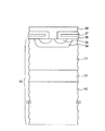
また、本発明者らは、実施例2として、図5に示すように表面構造がトレンチ構造のIGBTも作製した。図5に示す構成のIGBTでは、エピタキシャルウェハ30の、n-ドリフト層31の表面に、p+ベース領域44およびn+エミッタ領域45を形成し、トレンチエッチングによりトレンチを形成した後に、そのトレンチ内面にゲート絶縁膜46を形成した。そして、ゲート絶縁膜46の内側をポリシリコンで埋めてゲート電極47とし、さらにエミッタ電極48を形成した。その後、エピタキシャルウェハ30の設定厚さを130μmとしてバックグラインドをおこなった結果、n-ドリフト層31の厚さは125μmであり、n+バッファー層32の厚さは5μmであり、n-バックグラインドバッファー層40の厚さは1μmであった。
【0023】
そして、n-バックグラインドバッファー層40の研磨面にイオン注入および熱処理により、ピーク濃度が5×1017cm-3程度で深さが0.5μmのp+コレクタ層33を形成した。さらに、コレクタ電極39を形成し、その後、チップサイズにダイシングした。このようにして得られた図5に示す構成のIGBTは、図1に示す構成のIGBTと表面構造が異なるだけで、その他の構成は同じである。また、使用したエピタキシャルウェハ30の層構成、各層の比抵抗および厚さ、並びにウェハ全体の初期厚さも図1に示す構成のIGBTの場合と同じである。したがって、図1に示す構成と同様の構成については同じ符号を付して説明を省略する。
【0024】
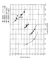
上述した実施例1のFS−IGBT(プレナー型)、実施例2のFS−IGBT(トレンチ型)、従来のNPT−IGBT(プレナー型、図8参照)および従来のPT−IGBT(プレナー型、図7参照)について、オン電圧とターンオフ損失とのトレードオフ関係を調べた結果を図6に示す。図6より、実施例1および実施例2とも、従来のIGBTよりも非常に良い特性を示すことがわかった。
【0025】
上述した実施の形態によれば、n-ドリフト層31、n+バッファー層32およびn-バックグラインドバッファー層40からなるエピタキシャルウェハ30を用い、n-ドリフト層31の表面にベース部およびエミッタ部を形成した後、n-バックグラインドバッファー層40をバックグラインド時のばらつきを吸収するバッファー層としてバックグラインドをおこない、その研磨面にコレクタ部を形成するため、オン電圧およびスイッチング損失がともに良好なIGBTを構成する半導体装置を安定して得ることができる。
【0026】
以上において本発明は種々変更可能である。たとえば、上述した実施の形態では第1導電型をn型とし、第2導電型をp型としたが、その逆でもよい。また、IGBTを構成する各層の比抵抗、厚さおよび不純物濃度、並びにエピタキシャルウェハ30の初期厚さなどの各数値は一例であり、本発明はこれに制限されるものではない。
【0027】
【発明の効果】
本発明によれば、第2のバッファー層が研磨時のばらつきを吸収するバッファー層となり、ドリフト層の上面にベース部およびエミッタ部を有し、第1および第2のバッファー層を介して第2のバッファー層の下面にコレクタ部を有する半導体装置が得られるので、オン電圧およびスイッチング損失がともに良好なIGBTを構成する半導体装置を安定して得ることができる。
【図面の簡単な説明】
【図1】本発明にかかる半導体装置(プレナー構造)の構造の一例を示す縦断面図である。
【図2】図1に示す半導体装置の製造途中の構造を示す縦断面図である。
【図3】図1に示す半導体装置の製造途中の構造を示す縦断面図である。
【図4】図1に示す半導体装置の製造途中の構造を示す縦断面図である。
【図5】本発明にかかる半導体装置(トレンチ構造)の構造の一例を示す縦断面図である。
【図6】本発明にかかる半導体装置と従来のIGBTについてオン電圧とターンオフ損失とのトレードオフ関係を示す特性図である。
【図7】従来のプレナー構造のPT−IGBTを示す縦断面図である。
【図8】従来のプレナー構造のNPT−IGBTを示す縦断面図である。
【符号の説明】
30 エピタキシャルウェハ
31 ドリフト層
32 バッファー層(第1のバッファー層)
33 コレクタ層
34,44 ベース領域
35,45 エミッタ領域
36,46 ゲート絶縁膜
37,47 ゲート電極
38,48 エミッタ電極
39 コレクタ電極
40 バックグラインドバッファー層(第2のバッファー層)[0001]
BACKGROUND OF THE INVENTION
The present invention relates to a semiconductor device and a manufacturing method thereof, and more particularly to a semiconductor device constituting an insulated gate bipolar transistor (hereinafter referred to as IGBT) and a manufacturing method thereof.
[0002]
[Prior art]
FIG. 7 is a longitudinal sectional view showing a conventional punch-through IGBT having a planar structure (hereinafter referred to as PT-IGBT). As shown in FIG. 7, the PT-IGBT includes a p + base region 14 on the surface of the n − drift layer 11 of the
[0003]
In the vertical IGBT, in order to reduce the on-voltage, it is necessary to increase the concentration of the p + collector layer 13 to reduce the electrical resistance as much as possible. As a result, the number of carriers injected from the p + collector layer 13 into the n − drift layer 11 becomes very large, causing a significant deterioration in switching loss and switching speed. Therefore, it is necessary to adjust device characteristics by introducing a lifetime killer.
[0004]
FIG. 8 is a longitudinal sectional view showing a conventional non-punch through type IGBT (hereinafter referred to as NPT-IGBT) having a planar structure. As shown in FIG. 8, the NPT-IGBT has a p + base region 24, an n + emitter region 25, a gate insulating film 26, a gate electrode 27 and an emitter electrode 28 on the surface of the FZ wafer constituting the n − drift layer 21. The p + collector layer 23 is formed on the back surface of the FZ wafer by a low temperature diffusion technology process, and the collector electrode 29 is further formed. In the NPT-IGBT, the n − drift layer 21 is not completely depleted when turned off, and the depletion layer does not reach the p + collector layer 23. In NPT-IGBT, device characteristics are adjusted by the concentration and thickness of the p + collector layer 23 without introducing a lifetime killer.
[0005]
Recently, in order to further reduce the loss, a field stop type IGBT (hereinafter referred to as FS-IGBT) having both advantages of PT-IGBT and NPT-IGBT has been proposed by Laska et al. (ISPSD'00, P.355-358, (2000)). The FS-IGBT includes an n − drift layer, an n + field stop layer, and a p + collector layer. By providing the n + field stop layer, the n − drift layer for obtaining a required breakdown voltage can be thinned, so that the on-voltage can be reduced.
[0006]
In addition, since the n + field stop layer and the p + collector layer are very thin, IEEE '97, p. In 213-216 (1997), since there are few carriers accumulated in each layer due to the Transparency Emitter effect mentioned by Porst et al., Switching loss can be suppressed. Further, in the FS-IGBT, as in the NPT-IGBT, the device characteristics are adjusted by the concentration of the p + collector layer, so that no lifetime killer is introduced.
[0007]
The following two methods are known as methods for manufacturing the above-described FS-IGBT or a similar device. The first method is a method of forming an n + field stop layer and a p + collector layer by performing ion implantation and thermal diffusion after polishing the FZ wafer to a thickness of about 100 to 120 μm. The second method is a method of polishing the p + collector layer to a thickness of about 0.5 μm using an epitaxial wafer that constitutes a conventional n − drift layer, n + buffer layer and p + collector layer. . In this second method, the n + buffer layer is the same as PT-IGBT (Matsudai et al., ISPSD '01, P.441-444, (2001)).
[0008]
[Problems to be solved by the invention]
However, in order to suppress an increase in leakage current at a high temperature, it is preferable that the n + field stop layer is thick. However, in the first method described above, the n + field stop layer and the p + collector layer are formed thick. In other words, the density becomes low, so that there is a problem that good electrical characteristics cannot be obtained. In order to obtain the Transparency Emitter effect, the thickness of the p + collector layer is preferably 1 μm or less. However, in the second method described above, when the p + collector layer is polished, it is actually about ± 3 μm. Therefore, there is a problem that the thickness of the p + collector layer must be 3 μm or more in consideration of the machining allowance.
[0009]
The present invention has been made in view of the above problems, and an object thereof is to provide a semiconductor device that constitutes an IGBT having excellent electrical characteristics. Another object of the present invention is to provide a method of manufacturing a semiconductor device that can stably manufacture a semiconductor device constituting an IGBT having excellent electrical characteristics.
[0010]
[Means for Solving the Problems]
In order to achieve the above object, according to the present invention , a first buffer layer of a first conductivity type having an impurity concentration higher than that of the drift layer is epitaxially grown on the drift layer of the first conductivity type. An epitaxial wafer is used in which a second buffer layer of the first conductivity type having an impurity concentration lower than that of the first buffer layer is epitaxially grown thereon. A base portion and an emitter portion are formed on the surface of the epitaxial wafer on the drift layer side. Further, after the surface of the epitaxial wafer on the second buffer layer side is polished to a predetermined wafer thickness, a collector portion is formed on the polished surface.
[0011]
According to this invention, the second buffer layer becomes a buffer layer that absorbs variations during polishing, and has a base portion and an emitter portion on the top surface of the drift layer, and the second buffer layer is interposed via the first and second buffer layers. A semiconductor device having a collector portion on the lower surface of the buffer layer is obtained.
[0012]
DETAILED DESCRIPTION OF THE INVENTION
Hereinafter, embodiments of the present invention will be described in detail with reference to the drawings. FIG. 1 is a longitudinal sectional view showing an example of the structure of a planar IGBT constituting a semiconductor device according to the present invention. This IGBT is manufactured using an
[0013]
The relationship between the n − drift layer thickness and the breakdown voltage value is shown below.
W = 2Ksε 0 · Vce / qNd
However, W = n − drift layer thickness, Vce = device breakdown voltage value, Ks = 11.7, ε 0 = 8.857 × 10 14 , q = 1.602 × 10 19 .
[0014]
Therefore, the thickness of the n − drift layer 31 is 0.1134 × Vce [μm] or less. For example, the thickness of the n − drift layer 31 required for a 1200 V breakdown voltage class element (actually a breakdown voltage of 1400 V is required). W = 0.1134 · Vce = 0.134 × 1400 = 159 [μm], and at least 159 [μm] is required.
[0015]
The impurity concentration of the n + buffer layer 32 is 1 × 10 14 cm −3 or more and 1 × 10 16 cm −3 or less. This is because if the impurity concentration of the n + buffer layer 32 is 1 × 10 14 cm −3 or less, the depletion layer cannot be stopped by the n + buffer layer 32 and the breakdown voltage is lowered. On the other hand, if the impurity concentration of the n + buffer layer 32 is 1 × 10 16 cm −3 or more, hole injection from the collector layer will be hindered, leading to a decrease in on-voltage and causing IGBT operation. It is because it will stop doing.
[0016]
Further, the thickness of the n + buffer layer 32 is 10 μm or less. This is because if the n + buffer layer 32 is too thick, switching loss increases during switching operation (particularly during turn-off), and the characteristics deteriorate. Therefore, in order to reduce switching loss, it is desirable that the thickness of the n + buffer layer 32 is as thin as 10 μm or less.
[0017]
Further, the impurity concentration of the n − back grind
[0018]
Further, the impurity concentration of the p + collector layer 33 is 10 times or more the average impurity concentration of the n + buffer layer 32. That is, in order to reduce the on-voltage of the IGBT, the impurity concentration of the collector layer is desirably 10 times or more the impurity concentration of the n + buffer layer. The thickness of the p + collector layer 33 is 1 μm or less. That is, the collector layer thickness is desirably 1 μm or less in order to reduce the switching loss due to the Transparency Emitter effect. The initial thickness of the
[0019]
The manufacturing process of the IGBT having the configuration shown in FIG. 1 will be described with reference to FIGS. First, as shown in FIG. 2, an
[0020]
Subsequently, as shown in FIG. 4, the n − back grind
[0021]
Example 1
The specifications of the IGBT having the configuration shown in FIG. 1 actually produced as Example 1 by the present inventors are as follows. The present invention is not limited to the following numerical values. In the case of the 1200 V breakdown voltage class, the specific resistance of the n − drift layer 31 with respect to the prepared
[0022]
(Example 2)
In addition, as Example 2, the present inventors also fabricated an IGBT having a trench structure as shown in FIG. In the IGBT having the configuration shown in FIG. 5, the p + base region 44 and the n + emitter region 45 are formed on the surface of the n − drift layer 31 of the
[0023]
Then, a p + collector layer 33 having a peak concentration of about 5 × 10 17 cm −3 and a depth of 0.5 μm was formed on the polished surface of the n −
[0024]
FS-IGBT (planar type) of Example 1 described above, FS-IGBT (trench type) of Example 2, conventional NPT-IGBT (planar type, see FIG. 8), and conventional PT-IGBT (planar type, diagram) FIG. 6 shows the result of examining the trade-off relationship between the on-state voltage and the turn-off loss. From FIG. 6, it was found that both Example 1 and Example 2 showed much better characteristics than the conventional IGBT.
[0025]
According to the embodiment described above, the
[0026]
In the above, the present invention can be variously changed. For example, in the above-described embodiment, the first conductivity type is n-type and the second conductivity type is p-type, but the opposite may be possible. Each numerical value such as the specific resistance, thickness and impurity concentration of each layer constituting the IGBT, and the initial thickness of the
[0027]
【Effect of the invention】
According to the present invention, the second buffer layer becomes a buffer layer that absorbs variation during polishing, and has a base portion and an emitter portion on the upper surface of the drift layer, and the second buffer layer is interposed via the first and second buffer layers. Since a semiconductor device having a collector portion on the lower surface of the buffer layer is obtained, a semiconductor device that constitutes an IGBT with good on-voltage and switching loss can be obtained stably.
[Brief description of the drawings]
FIG. 1 is a longitudinal sectional view showing an example of the structure of a semiconductor device (planar structure) according to the present invention.
2 is a longitudinal sectional view showing a structure in the middle of manufacturing the semiconductor device shown in FIG. 1;
3 is a longitudinal sectional view showing a structure in the middle of manufacturing the semiconductor device shown in FIG. 1;
4 is a longitudinal sectional view showing a structure in the middle of manufacturing the semiconductor device shown in FIG. 1;
FIG. 5 is a longitudinal sectional view showing an example of the structure of a semiconductor device (trench structure) according to the present invention.
FIG. 6 is a characteristic diagram showing a trade-off relationship between on-state voltage and turn-off loss for a semiconductor device according to the present invention and a conventional IGBT.
FIG. 7 is a longitudinal sectional view showing a PT-IGBT having a conventional planar structure.
FIG. 8 is a longitudinal sectional view showing a conventional planar structure NPT-IGBT.
[Explanation of symbols]
30
33
Claims (3)
所定のウェハ厚さになるまで前記第2のバッファー層の露出面を研磨する工程と、 Polishing the exposed surface of the second buffer layer to a predetermined wafer thickness;
前記第2のバッファー層の研磨面に第2導電型のコレクタ層およびコレクタ電極を形成する工程と、 Forming a collector layer and a collector electrode of a second conductivity type on the polished surface of the second buffer layer;
を含むことを特徴とする半導体装置の製造方法。 A method for manufacturing a semiconductor device, comprising:
Priority Applications (1)
| Application Number | Priority Date | Filing Date | Title |
|---|---|---|---|
| JP2001260976A JP4967209B2 (en) | 2001-08-30 | 2001-08-30 | Manufacturing method of semiconductor device |
Applications Claiming Priority (1)
| Application Number | Priority Date | Filing Date | Title |
|---|---|---|---|
| JP2001260976A JP4967209B2 (en) | 2001-08-30 | 2001-08-30 | Manufacturing method of semiconductor device |
Publications (2)
| Publication Number | Publication Date |
|---|---|
| JP2003069020A JP2003069020A (en) | 2003-03-07 |
| JP4967209B2 true JP4967209B2 (en) | 2012-07-04 |
Family
ID=19088087
Family Applications (1)
| Application Number | Title | Priority Date | Filing Date |
|---|---|---|---|
| JP2001260976A Expired - Lifetime JP4967209B2 (en) | 2001-08-30 | 2001-08-30 | Manufacturing method of semiconductor device |
Country Status (1)
| Country | Link |
|---|---|
| JP (1) | JP4967209B2 (en) |
Families Citing this family (7)
| Publication number | Priority date | Publication date | Assignee | Title |
|---|---|---|---|---|
| JP2005303218A (en) * | 2004-04-16 | 2005-10-27 | Renesas Technology Corp | Semiconductor device and its manufacturing method |
| JP4878739B2 (en) * | 2004-05-12 | 2012-02-15 | 新電元工業株式会社 | Manufacturing method of semiconductor device |
| JP5033335B2 (en) * | 2006-02-21 | 2012-09-26 | ルネサスエレクトロニクス株式会社 | Semiconductor device and inverter device using the same |
| JP5326481B2 (en) * | 2008-10-14 | 2013-10-30 | 富士電機株式会社 | Semiconductor device and manufacturing method of semiconductor device |
| JP5262552B2 (en) * | 2008-10-14 | 2013-08-14 | 富士電機株式会社 | Semiconductor device manufacturing method and semiconductor device |
| JP5639940B2 (en) * | 2011-03-25 | 2014-12-10 | 新電元工業株式会社 | Insulated gate bipolar transistor |
| US20130277793A1 (en) * | 2012-04-24 | 2013-10-24 | Fairchild Korea Semiconductor, Ltd. | Power device and fabricating method thereof |
Family Cites Families (6)
| Publication number | Priority date | Publication date | Assignee | Title |
|---|---|---|---|---|
| JPS6445173A (en) * | 1987-08-13 | 1989-02-17 | Fuji Electric Co Ltd | Conductive modulation type mosfet |
| US5872028A (en) * | 1996-09-05 | 1999-02-16 | Harris Corporation | Method of forming power semiconductor devices with controllable integrated buffer |
| JP2000223705A (en) * | 1999-01-29 | 2000-08-11 | Nissan Motor Co Ltd | Semiconductor device |
| JP2000260778A (en) * | 1999-03-11 | 2000-09-22 | Toshiba Corp | Semiconductor device and manufacture |
| JP2001077357A (en) * | 1999-08-31 | 2001-03-23 | Toshiba Corp | Semiconductor device |
| JP3906076B2 (en) * | 2001-01-31 | 2007-04-18 | 株式会社東芝 | Semiconductor device |
-
2001
- 2001-08-30 JP JP2001260976A patent/JP4967209B2/en not_active Expired - Lifetime
Also Published As
| Publication number | Publication date |
|---|---|
| JP2003069020A (en) | 2003-03-07 |
Similar Documents
| Publication | Publication Date | Title |
|---|---|---|
| US9620630B2 (en) | Injection control in semiconductor power devices | |
| JP4351745B2 (en) | Semiconductor device | |
| TWI459554B (en) | Method of minimizing field stop insulated gate bipolar transistor (igbt) buffer and emitter charge variation | |
| CN101976683B (en) | Insulated gate bipolar transistor and manufacturing method thereof | |
| KR101237345B1 (en) | Power semiconductor device using silicon substrate as field stop layer and method of manufacturing the same | |
| US20040084722A1 (en) | Power semiconductor device | |
| JP3719323B2 (en) | Silicon carbide semiconductor device | |
| TW201232664A (en) | New topside structures for an insulated gate bipolar transistor (IGBT) device to achieve improved device performances | |
| US7569431B2 (en) | Semiconductor device and manufacturing method thereof | |
| JP4904625B2 (en) | Semiconductor device | |
| JP2008042013A (en) | Method of manufacturing semiconductor device | |
| JPH05102497A (en) | Power semiconductor element | |
| US11239352B2 (en) | Self-aligned and robust IGBT devices | |
| JP4967209B2 (en) | Manufacturing method of semiconductor device | |
| JP2002261281A (en) | Manufacturing method of insulated gate bipolar transistor | |
| JP2004221370A (en) | Semiconductor device | |
| WO2000031800A1 (en) | Semiconductor device and fabrication method therefor | |
| JP4904635B2 (en) | Semiconductor device and manufacturing method thereof | |
| JP3969256B2 (en) | Manufacturing method of semiconductor device | |
| WO2024052952A1 (en) | Semiconductor device, method for controlling semiconductor device, and method for producing semiconductor device | |
| JP3280232B2 (en) | Semiconductor device | |
| JPH0982955A (en) | Manufacture of semiconductor device | |
| WO1996032749A1 (en) | Semiconductor device having planar type high withstand voltage vertical devices, and production method thereof | |
| TWI607563B (en) | With a thin bottom emitter layer and in the trenches in the shielded area and the termination ring Incoming dopant vertical power transistors | |
| JP2004193630A (en) | High withstand voltage semiconductor element |
Legal Events
| Date | Code | Title | Description |
|---|---|---|---|
| A621 | Written request for application examination |
Free format text: JAPANESE INTERMEDIATE CODE: A621 Effective date: 20080715 |
|
| A711 | Notification of change in applicant |
Free format text: JAPANESE INTERMEDIATE CODE: A712 Effective date: 20091112 |
|
| RD03 | Notification of appointment of power of attorney |
Free format text: JAPANESE INTERMEDIATE CODE: A7423 Effective date: 20091112 |
|
| RD04 | Notification of resignation of power of attorney |
Free format text: JAPANESE INTERMEDIATE CODE: A7424 Effective date: 20091112 |
|
| A711 | Notification of change in applicant |
Free format text: JAPANESE INTERMEDIATE CODE: A712 Effective date: 20110422 |
|
| A977 | Report on retrieval |
Free format text: JAPANESE INTERMEDIATE CODE: A971007 Effective date: 20111207 |
|
| A131 | Notification of reasons for refusal |
Free format text: JAPANESE INTERMEDIATE CODE: A131 Effective date: 20111213 |
|
| A521 | Written amendment |
Free format text: JAPANESE INTERMEDIATE CODE: A523 Effective date: 20120213 |
|
| TRDD | Decision of grant or rejection written | ||
| A01 | Written decision to grant a patent or to grant a registration (utility model) |
Free format text: JAPANESE INTERMEDIATE CODE: A01 Effective date: 20120306 |
|
| A01 | Written decision to grant a patent or to grant a registration (utility model) |
Free format text: JAPANESE INTERMEDIATE CODE: A01 |
|
| A61 | First payment of annual fees (during grant procedure) |
Free format text: JAPANESE INTERMEDIATE CODE: A61 Effective date: 20120319 |
|
| FPAY | Renewal fee payment (event date is renewal date of database) |
Free format text: PAYMENT UNTIL: 20150413 Year of fee payment: 3 |
|
| R150 | Certificate of patent or registration of utility model |
Free format text: JAPANESE INTERMEDIATE CODE: R150 Ref document number: 4967209 Country of ref document: JP Free format text: JAPANESE INTERMEDIATE CODE: R150 |
|
| R250 | Receipt of annual fees |
Free format text: JAPANESE INTERMEDIATE CODE: R250 |
|
| R250 | Receipt of annual fees |
Free format text: JAPANESE INTERMEDIATE CODE: R250 |
|
| R250 | Receipt of annual fees |
Free format text: JAPANESE INTERMEDIATE CODE: R250 |
|
| R250 | Receipt of annual fees |
Free format text: JAPANESE INTERMEDIATE CODE: R250 |
|
| R250 | Receipt of annual fees |
Free format text: JAPANESE INTERMEDIATE CODE: R250 |
|
| R250 | Receipt of annual fees |
Free format text: JAPANESE INTERMEDIATE CODE: R250 |
|
| R250 | Receipt of annual fees |
Free format text: JAPANESE INTERMEDIATE CODE: R250 |
|
| EXPY | Cancellation because of completion of term |