JP4965025B2 - Column redundancy circuit with reduced signal path delay - Google Patents
Column redundancy circuit with reduced signal path delay Download PDFInfo
- Publication number
- JP4965025B2 JP4965025B2 JP2000580093A JP2000580093A JP4965025B2 JP 4965025 B2 JP4965025 B2 JP 4965025B2 JP 2000580093 A JP2000580093 A JP 2000580093A JP 2000580093 A JP2000580093 A JP 2000580093A JP 4965025 B2 JP4965025 B2 JP 4965025B2
- Authority
- JP
- Japan
- Prior art keywords
- column
- redundant
- normal
- signal
- driver
- Prior art date
- Legal status (The legal status is an assumption and is not a legal conclusion. Google has not performed a legal analysis and makes no representation as to the accuracy of the status listed.)
- Expired - Fee Related
Links
- 230000015654 memory Effects 0.000 claims abstract description 56
- 230000002950 deficient Effects 0.000 claims abstract description 37
- 239000004065 semiconductor Substances 0.000 claims abstract description 23
- 230000004044 response Effects 0.000 claims description 26
- 230000007547 defect Effects 0.000 claims description 6
- 230000004913 activation Effects 0.000 claims description 3
- 230000003213 activating effect Effects 0.000 claims 3
- 230000008878 coupling Effects 0.000 claims 1
- 238000010168 coupling process Methods 0.000 claims 1
- 238000005859 coupling reaction Methods 0.000 claims 1
- 101000835860 Homo sapiens SWI/SNF-related matrix-associated actin-dependent regulator of chromatin subfamily B member 1 Proteins 0.000 description 21
- 102100025746 SWI/SNF-related matrix-associated actin-dependent regulator of chromatin subfamily B member 1 Human genes 0.000 description 21
- 238000000034 method Methods 0.000 description 13
- 238000010586 diagram Methods 0.000 description 9
- 230000003111 delayed effect Effects 0.000 description 6
- 238000011156 evaluation Methods 0.000 description 6
- 230000007246 mechanism Effects 0.000 description 6
- 230000007704 transition Effects 0.000 description 6
- 238000013459 approach Methods 0.000 description 4
- 239000003990 capacitor Substances 0.000 description 3
- 238000005516 engineering process Methods 0.000 description 3
- 230000006870 function Effects 0.000 description 3
- 238000012986 modification Methods 0.000 description 3
- 230000004048 modification Effects 0.000 description 3
- 101000616718 Homo sapiens Sialate O-acetylesterase Proteins 0.000 description 2
- 102100021837 Sialate O-acetylesterase Human genes 0.000 description 2
- 230000009977 dual effect Effects 0.000 description 2
- 230000014509 gene expression Effects 0.000 description 2
- 230000010354 integration Effects 0.000 description 2
- 230000008569 process Effects 0.000 description 2
- 238000012360 testing method Methods 0.000 description 2
- 230000008901 benefit Effects 0.000 description 1
- 230000000295 complement effect Effects 0.000 description 1
- 239000000470 constituent Substances 0.000 description 1
- 238000013461 design Methods 0.000 description 1
- 238000001514 detection method Methods 0.000 description 1
- 230000001360 synchronised effect Effects 0.000 description 1
Images


Classifications
-
- G—PHYSICS
- G06—COMPUTING; CALCULATING OR COUNTING
- G06F—ELECTRIC DIGITAL DATA PROCESSING
- G06F12/00—Accessing, addressing or allocating within memory systems or architectures
- G06F12/02—Addressing or allocation; Relocation
-
- G—PHYSICS
- G11—INFORMATION STORAGE
- G11C—STATIC STORES
- G11C29/00—Checking stores for correct operation ; Subsequent repair; Testing stores during standby or offline operation
- G11C29/70—Masking faults in memories by using spares or by reconfiguring
- G11C29/78—Masking faults in memories by using spares or by reconfiguring using programmable devices
- G11C29/80—Masking faults in memories by using spares or by reconfiguring using programmable devices with improved layout
- G11C29/808—Masking faults in memories by using spares or by reconfiguring using programmable devices with improved layout using a flexible replacement scheme
Abstract
Description
【0001】
この発明は半導体メモリに関し、特に欠陥のあるカラムを冗長カラムで置きかえるための柔軟で効率的な回路を備える半導体メモリに関する。
【0002】
従来の技術
半導体ダイナミックランダムアクセスメモリ(DRAMs)は、典型的にはワードラインとこのワードラインに交差するカラムから形成される。ローラインとカラムの交差部分にそれぞれに近接するキャパシタは電荷を蓄積し、格納されるデータを示す。これらキャパシタは、ローライン上に適当な電圧を受け取って充電したりあるいは放電させるために、アクセストランジスタによりカラムに結合されている。ローライン及びカラムは、ロー(またはX)デコーダ及びカラム(またはY)デコーダ手段により特定のキャパシタに読み書きできるように選択される。
【0003】
カラムあるいは関連要素に関連して物理的欠陥が生じることがときどきある。このためRAMは通常は、余分なメモリ要素及びカラム回路の備えである冗長(予備)カラムを含む。余分なメモリ及び欠陥のあるカラムの代わりにこのメモリにアクセスするために必要な冗長デコーダは貴重な半導体チップの領域を使用してメモリの領域の効率を減少させる。
【0004】
同期型ダイナミックランダムアクセスメモリ(SDRAMs)において、カラム冗長方式を提供するためさまざまな手法が実現されている。これらの中には、アドレス比較手法、アドレス検出器手法、シフト器手法、及びアドレスまたはデータステアリング手法とともにこれらの組み合わせがある。例えば、これらの手法の最初のものにおいて、図1に示されるように再生成されたYアドレス信号(PY1:N)をヒューズを通して送り、冗長カラムエネーブル信号(RCE)を発生させるYアドレスコンパレータを利用している。冗長コンパレータ2に関連づけられたこれらヒューズは固有の容量及び抵抗をもち、Y冗長パスに余分な遅延を加えてしまう。
【0005】
ふたつめの手法はYアドレスデコーダ4に関し、ここでのYアドレス信号(AY(N−1):0)は、図2に示されるようにヒューズを通してプリチャージ接続点に接続するとともにそれぞれが冗長カラムエネーブル信号を発生するNMOSゲートを制御する。Yアドレスがあるヒューズプログラミングパターンに一致するとき、カラム冗長エネーブル信号(COL_RED_EN)が、現在のYアドレスに対応するカラムが冗長カラムで置きかえられることを示すために高レベルに維持される。この冗長検出回路のために通常のパスと冗長カラムのパスの間のタイミングは通常異なる。このタイミングの違いを調整するための付加的なロジック回路、すなわち冗長パスで遅くなったタイミングを補償するために通常のアドレス信号パスに用いられなければならない遅延回路が必要とされる。
【0006】
他の手法として知られるシフト置換YデコーダはYデコーダにおいてヒューズを利用するが、その信号パスに接続されていない。一般的に、2つのY選択線はヒューズのひとつのグループを分け合っている。カラムを置き換えるために、そのカラムはYデコーダの内部のヒューズを切断することにより動作しなくなる。欠陥のあるブロックへのYドライバのアクセスを隣接するドライバへシフトすることにより置換は完了する。このシステムの利点は、ヒューズがカラムアドレスパスに接続されていないため、通常のパスと冗長パスの間でタイミングの違いが存在しないという点である。さらに、ブロック置換が可能である(欠陥が存在するカラムは各ブロックの異なるデコーディングを用いて各ブロックで欠陥を直すことができる)。このシステムの欠点は、2つの隣接するY選択線を同時に置き換えなければならず、この手法は他の手法に比べて柔軟性がない点である。さらに、カラムに一方向シフティングを必要とする。
【0007】
図3において、冗長回路10は、チェン他からモサイドテクノロジーズインコーポレイテッドに譲渡された合衆国特許出願第08/904,153に開示された発明の実施の形態に係るアドレスステアリング手法を用いて実現したものである。この手法によれば、各Yデコーダは、ヒューズ回路14にプログラムされた情報に従ってカラム選択信号を通常または冗長パスのいずれか一方に向けるNMOSマルチプレクサ12からなる。マルチプレクサのNMOSトランジスタはこれらを完全にオンするためにはVDDよりも高い電圧を必要とするので、NMOSトランジスタはチップ上で昇圧された電源電圧VPPに接続して用いられ、適切なパスを選択する。冗長選択線RYSEL16は長く、かなり大きなRC遅延が存在する。この実装例において、2つの冗長カラムドライバが64の通常カラムによりアクセス可能であるが、冗長ドライバはそのブロック内においてのみ欠陥カラムを置き換えることに用いられるにすぎず、四分の一(quadrant)内のほかのどのブロックの欠陥カラムも置き換えることに用いることができない。この柔軟性の欠如は、64M SDRAMの集積度から256M SDRAMの集積度へ移行するときに耐えがたいことが証明されている。さらに、冗長選択線RYSEL16の長さは256M世代のSDRAMにとって遅すぎる設計の原因となる。
【0008】
したがって、通常のパスと冗長カラムパスの間のタイミングの違いを減らし、ヒューズの数を減らして欠陥カラムを修理する際の柔軟性を増やし、大きなメモリの速度要求に適応することができる冗長手法に対する要求が存在したのである。
【0009】
発明の要約
この発明は、通常のアドレスパスと冗長カラムのアドレスパスの間のタイミングの違いを最小化するとともに欠陥カラムを直すときに切断が必要とされるヒューズの数を最小化する半導体メモリにおけるカラム冗長方法及び装置を提供するためになされたものである。
【0010】
この発明によれば、
a)通常カラムデコーダにより選択的に動作可能にされる複数の通常メモリカラムと、
b)冗長カラムデコーダにより選択的に動作可能にされる冗長メモリカラムとを備え、前記通常及び冗長カラムデコーダはカラムクロック信号に応答し、
c)前記冗長カラムデコーダからの出力に応答して、通常ドライバまたは対応する冗長ドライバのいずれか一方に前記カラムクロック信号を切り換える局所信号分配回路とを備える半導体メモリ装置が提供される。
【0011】
好適な実施例の詳細な説明
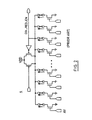
以下の説明において、図面の同様な要素は類似の数字で参照される。図4を参照すると、この発明の一般的な実施の形態に係るカラム冗長機構を実装するSDRAMの部分の配置が符号60で示されている。さらに具体的には、示されているカラム冗長機構は、メモリチップが4つのバンク(バンク当たり16×32ブロック、すなわちローラインの中の16ブロック、カラムの32ブロック)に分割される256M(Mbit)SDRAM用である。各バンクはローデコーダによりカラム方向に2つの半分のバンクに物理的に分離され、各半分のバンクは16カラムブロックを備える。各ブロックは64の通常カラム62と1つの冗長カラムを備える。図中に示される部分60は、BLOCK1、BLOCK2、BLOCK3及びBLOCK4と番号が付けられたブロックをもち、この配置はひとつの半分のバンクについて4回、バンク全体について8回繰り返される。各ブロックに関連付けられている冗長カラム64は各ブロックの右手側に示されている。各ブロックはコアYデコーダドライバ回路(YDEC)66(通常カラムデコーダドライバ66)(注:コア回路は、物理的及び機能的にメモリアレイに関連づけられている回路を言う。カラムとYという用語は相互に交換可能に用いられる)と、冗長Yデコーダ(冗長カラムデコーダRY)68と、冗長カラムドライバ(RYDEC)70とを備える。コアYデコーダドライバ回路(YDEC)66はチップの全体のYデコーディングの第2段階である。コアYデコーダドライバ回路(YDEC)66はYプリデコーダ(図示されていない)の出力PYから入力を得て、カラムデコーディングを完遂する。カラムデコーディングの第1段階は、グローバルカラムアドレス信号ACL[0:8](図示されていない)から次のプリデコードされたYアドレス:PY0_1_2(7:0)、PY3_4(3:0)、PY5_6(3:0)、PY7_8(3:0)を発生するYプリデコーダにより実行される。これらのアドレスの全ては、コアYデコーダドライバ回路(YDEC)66及び冗長Yデコーダ(RY)68へプリデコードされたアドレス信号を運ぶバスPYとして図4に一般的に示されている。全てSDRAMの分野においてよく知られた機能である、Yアドレスラッチ、バースト制御、インターリーブ制御、シーケンシャルバースト、インターリーブバースト及びYアドレスプリフェッチ等の論理機能は、全てYプリデコーダ回路に実装されている。
【0012】
上述のように、各ブロックはそのブロックの側に位置するひとつの冗長カラム64と冗長Yデコーダ(RY)68を備える。冗長Yデコーダ(RY)68とその対応するBLOCKコアYデコーダは同じブロック選択信号(BSEL)を共用する。結果として、ブロック選択信号BSELを切り換えることにより、ひとつのブロックの冗長カラムはバンク内の任意の隣接する4つのブロックのひとつの欠陥通常カラムを置き換えることに使用できる。さらに詳細は以下で説明される。コアYデコーダドライバ回路(YDEC)66及び冗長カラム64は共通のY選択クロック信号YSGによりクロックされる。4つの関連する冗長Yデコーダ(RY)68の概略構造、これらのコアYデコーダ及びコアI/Oとの関係は図4に示されている。
【0013】
この発明の実施の形態において、YSG信号は局所的に分配される。バンクの中央にあるYSG信号ドライバはバンク全体にわたってYSG信号を送る。YSG1、YSG2、YSG3などと示され、図9においてその詳細が示される、局所YSG信号分配回路72は各ブロックに備えられる。局所YSG信号分配回路72のそれぞれは、冗長Yデコーダ(RY)68からの出力RDECに応答して、コアYデコーダドライバ回路(YDEC)66または対応する冗長カラムドライバ70のいずれか一方にYSG信号を切り換えてドライブする。YSG1、YSG2、YSG3などの局所YSG信号分配回路72は、図9に示されるようにBUSL及び/BUSL信号(負論理を「/」で表す。以下同じ)によりクロックされ、2クロックサイクルの間それに対応する冗長Yデコーダ(RY)68の出力RDECをラッチする。もしラッチされた論理値が高(high)であるならば、YSG信号は冗長カラムドライバ70へ切り換えられ、冗長カラム64をドライブする。もしラッチされた論理値が低(low)であるならば、YSG信号はコアYデコーダドライバ回路(YDEC)66へ切り換えられ、通常カラムをドライブする。
【0014】
一般的に、隣接する奇数または偶数のブロック内の4つの冗長Yデコーダ(RY1〜RY4)68は4つのブロック全てにより共用され、これら4つのブロック内のいかなる欠陥通常カラムを置き換えるためにも使用することができる。冗長Yデコーダ(RY)68の/DB_CTL出力は4入力ANDゲート68bに接続されている。このゲートからの出力/RY10F4は4つの冗長Yデコーダ(RY1〜RY4)68に共有される。したがって、冗長Yデコーダ(RY)68が動作しているとき、その出力信号/DB_CTLは低(low)にセットされ、そして/RY10F4は低(low)にセットされ、冗長Yデコーダ(RY)68が使用中であることをコアI/O回路(コアデータパス回路)に知らせる。
【0015】
あるブロック内で通常カラムが選択されているとき、BSEL信号は高(high)になる。対応するコアI/Oはイネーブルされる必要があり、コアI/O制御信号DBSW_CTLは高(high)になる。もし、選択された通常カラムが不良であるなら、それは現在のブロックの内部または外部いずれか一方の冗長Yデコーダ(RY)68により置き換えられる。たとえBSELが高(high)のままであるとしてもこの欠陥の場合、DBSW_CTLは高(high)になるかどうかは、欠陥が置換される位置に依存する。DBSW_CTL信号は、選択されたカラムデータをデータバスに結合する、適切なデータバスのCMOSパスゲート67を切り換える。/RY10F4及びBSELは図6に記述される冗長Yデコーダ(RY)68へ入力され、出力DBSW_CTLを決定するために用いられる。これはコアI/Oスイッチを制御する。コアI/Oスイッチの規則は次の表に示される。
【0016】
【表1】

図示されている256M SDRAMにおいて、全ての制御信号とデータバスの2つのバージョンがある。ひとつはB0と記号が付されたものであり、他方はB1と記号が付されたものである。B0信号がアクティブの間、B1信号はプリチャージしている。B1信号がアクティブの間、B0信号はプリチャージしている。このように、より高速な動作のためにプリチャージ時間を隠している。この二重データバスアーキテクチャは、モサイドテクノロジーズに譲渡された合衆国特許第5,416,743号に記載されており、ここに言及することにより本明細書に組み込まれる。BUSL及び/BUSL信号はB0とB1信号の間の切換の予定を制御する。
【0018】
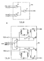
ここで図5(a)及び図5(b)を参照すると、コアYデコーダ66a及びカラムドライバ回路66bの回路図が示されている。組み合わされた回路は図4のブロック66に概略的に示されている。コアYデコーダ66aは、Yプリデコーダ出力PY0_1_2,PY3_4,PY5_6及びPY7_8を受ける一組のNANDゲート72及び74を備える。NANDゲート72及び74からの出力はNORゲート76で組み合わされ、デコードされた出力信号DECを提供する。デコーダ回路66aは4入力ANDゲートと等価である。コアYデコーダ66aからの出力DECは、図5(a)に示されるようにカラムドライバ回路66bに結合される。
【0019】
通常または冗長のカラムドライバ回路66bは、信号BUSL及び/BUSLとともに出力信号DECにより制御される各CMOSパスゲート82及び84でYクロックエネーブル信号/YSG_B0及び/YSG_B1を受ける。クロックエネーブル信号/YSG_B0及び/YSG_B1は適当な時間にそのCMOSパスゲートを通過してインバータ86に到達し、このインバータはBUSLまたは/BUSL信号の状態に応じて信号Y_B0またはY_B1で対応するカラムをドライブする。このように、デコードされた信号DECはCMOSパスゲート82及び84を制御する。
【0020】
図4に示される全体のコアYデコーダドライバ回路(YDEC)66は、図5(a)及び図5(b)に示される2つの部品で作られてもよい。例えば、Yアドレスが9ビットであるならば、512の異なるデコーディング出力を備える。偶数ビット及び奇数ビットはそれぞれ4つの偶数ブロック及び4つの奇数ブロックをドライブするように分離されていてもよい。その配列は、半分のバンクのための完全なコア幅デコーダを実現するためにそれ自身を2回繰り返したり、全体のバンクために4回繰り返す。
【0021】
図6を見ると、図4の冗長Yデコーダ(RY)68の詳細な図面が示されている。冗長Yデコーダ(RY1、RY2、・・・RYN)68は、冗長カラムへのアクセスが要求されているかどうかを判定する。これらの冗長Yデコーダ(RY)68はアドレス比較機構を利用してこの判定を行う。繰り返すが、各メモリブロックはそのブロック側に位置するひとつの冗長カラムを備える。冗長Yデコーダ(RY)68及びその対応するコアYデコーダYDECは同じブロック選択信号(BSEL)を共有する。図6に示される冗長Yデコーダ(RY)68は、プリデコードされたアドレスPY0_1_2、PY3_4,PY5_6及びPY7_8を受ける一組のアドレス比較回路90を含む。各アドレス比較回路90は単一のアドレスにプログラムされることができ、したがって冗長Yデコーダ(RY)68は2つの冗長アドレスにプログラムされることができる。アドレス比較回路90の詳細は図7を参照して説明される。
【0022】
通常カラムはブロック内の上側または下側の部分に分離してアドレスされている可能性があるので、ローアドレス信号AX12は冗長Yデコーダ(RY)68へ供給されて上側または下側のカラム部分の選択を行う。ローアドレス信号AX12は、アドレス比較回路92及び94からのそれぞれの出力を受ける一組のCMOSパスゲート96及び98の制御入力に結合される。従って、ひとつの冗長カラムは、2つの異なるアドレスの通常カラムの下側半分と通常カラムの上側半分を置き換えに用いることができ、またその逆も可能である。/RY信号はインバータ99に結合されてRDEC信号をドライブする。これは次に図5(b)に示されたカラムドライバ回路66b及び図4に示された局所YSG信号分配回路72をドライブする。
【0023】
回路は、またINI1及びINI0発生回路を含む。一般的にはこの回路はメインのINI信号線からドライブされる直列に接続されたインバータ100の連鎖を備え、INI0及びINI1信号は連鎖に沿うタップから取られる。
【0024】
図7を参照すると、図6のアドレス比較回路90の詳細が示されている。プリデコーダ(図4)はプリデコードされた出力の4つのグループ:PY0_1_2,PY3_4,PY5_6及びPY7_8をもつので、アドレス比較回路はプログラム可能なヒューズ回路142の4つのグループを備える。ヒューズ回路の各グループ142は、図8に示されるヒューズ状態評価回路180に関連付けられた4つのヒューズを含む。ひとつのグループの構成ヒューズ評価回路のそれぞれへの入力は各グループのプリデコードされたカラムアドレス信号、すなわちPY0_1_2,PY3_4,PY5_6またはPY7_8から得られる。グループ142のそれぞれのヒューズからの出力PY_OUTは、それぞれの信号PY_OUT1、PY_OUT2、PY_OUT3及びPY_OUT4を供給するように組み合わされる。これらの信号は、アドレス組み合わせ回路146で組み合わされる前に、初期化回路144を通過する。アドレス組み合わせ回路146は本質的には図6で示される冗長選択信号/RYを出力する4入力NANDゲートである。これらの回路部のそれぞれは以下に詳しく説明される。
【0025】
アドレス比較回路90の動作は次のとおりである。欠陥カラムがなく冗長カラムを必要としないとき、いずれのヒューズ回路も切断されず、PY_OUT線は、回路の初期化回路144により全てロジック低(low)に初期化される。これは、全ての非欠陥カラムのヒューズが切断される一方で、欠陥アドレスのヒューズは損なわれていないままにされていた、いくつかの先行技術のアドレス比較の具体例と対照的である。この手法は冗長プログラミングプロセスをかなり複雑にする。初期化回路144は一組のNORゲート148及び150を備え、これらのそれぞれはその入力部でそれぞれのPY_OUT信号を受けるように接続されている。各NORゲート入力は、それぞれNMOSトランジスタ152及び154に結合される。これらのトランジスタのゲートはそれぞれのNORゲート出力に接続されている。従って、NORゲート148、150への全てのロジック低(low)PY_OUT入力について、フィードバックトランジスタを通るフィードバック接続がさらに入力をロジック低(low)にラッチする間、NORゲートの出力はロジック高(high)である。線PY_OUTの同じロジック低(low)信号がNANDゲート155及び156に供給され、そのためこれらの出力にロジック高(high)を生成する。信号CST_BLKは、通常は高(high)であるブロック冗長試験信号であり、それによりNANDゲート157及び158をイネーブルする。NANDゲート155及び156からの出力がロジック高(high)でありかつCST_BLK信号がロジック高(high)であると、NANDゲート157及び158からの両方の出力はロジック低(low)である。これは次にNANDゲート160のロジック高(high)出力を生成し、冗長性は使用されていない、すなわち/RYはロジック高(high)であることを示す。
【0026】
もし、欠陥位置が試験中に発見されると、適切なプレデコーダカラムアドレスが、先に記述されたようにヒューズ回路グループのそれぞれにプログラムされる。アドレス比較回路出力は初期化装置に優先する(この処理はさらに詳しく後述される)ので、結果として、プログラミング信号線PY_OUT1,PY_OUT2,PY_OUT3及びPY_OUT4はプリデコードされた信号を受けてすべてロジック高(high)に設定される。その結果、NANDゲート155及び156に2つのロジック高(high)入力が供給されるので、それぞれのゲートはロジック低(low)出力を提供し、この低(low)出力がNANDゲート157及び158で通常高(high)のCST_BLK信号と結合されたとき、NANDゲート160に2つのロジック高(high)入力信号を供給し、このゲートからアクティブ低(low)出力信号/RYが供給され、冗長性の使用を示す。この発明の実施の形態において、第一に、欠陥アドレスが検出されないときヒューズは切断される必要はないのに対して、図1の先行技術のアドレス比較手法において全てのヒューズは切断されなければならない点に注意することは重要である。第二に、欠陥アドレスが検出され、欠陥アドレスをプログラムするとき、この発明の実施の形態において、先行技術のアドレス比較機構で12個のヒューズを切断しなければならないのに対して、この発明の実施の形態において、わずか4つのヒューズが切断されなければならないにすぎない。これらの違いにより、冗長プログラミング機能の相当の簡易化が実現されるのである。
【0027】
図8を参照すると、図7のヒューズ状態評価回路180の詳細な回路図が示されている。上述のように、ヒューズ状態評価回路180はそのPY_IN端子にプリデコードされたアドレス信号のうちのひとつを受け、この信号は次にNMOS及びPMOSトランジスタの183及び184それぞれにより形成されるCMOSパスゲート182に接続される。CMOSパスゲート182の出力は信号PY_OUTである。CMOSパスゲート182はヒューズ素子186により制御される。CMOSパスゲート182に対する初期状態はNANDゲート188により設定され、このNANDゲートは信号INI0及びINI1から受ける入力により決定される初期状態をもつ。INI0及びINI1信号は、図6に示されるように、INI1の前にINI0が来るように互いに少しだけ遅延させたバージョンである。
【0028】
フィードバックPMOSトランジスタ190は、NANDゲート188の出力に接続されたゲートと、NANDゲート188の入力188bに接続されたドレインを備え、ハーフラッチを形成する。フィードバックトランジスタ190はプログラムされた冗長アドレスをラッチするために使用される。INI1信号は、NANDゲート188のもう一方の入力188aのうちのひとつ及びひとつの端が接地されたヒューズ186の他の端に接続されたソースをもつNMOSトランジスタ192のゲートへ直接加えられる。NMOSトランジスタ192のドレイン端子はPMOSトランジスタ194のドレイン端子に接続され、このPMOSトランジスタ194のソースはVDD電源に接続される。INI0信号はPMOSトランジスタ194のゲートに加えられる。PMOSトランジスタ194及びNMOSトランジスタ192の間の共通ドレイン接続はNANDゲート188の最初の入力188bに接続される。NANDゲート188からの出力はインバータ196を経由してCMOSパスゲート182の2つのトランジスタの一方のNMOSトランジスタの183に接続され、これをドライブする。
【0029】
ヒューズ状態は次のように評価される。信号INI0及びINI1はPOWER_OK信号から発生され、INI1はINI0よりも遅延させられる。最初に、INI0及びINI1の両方が低(low)であり、CMOSパスゲート182はオープンの状態であり、プリデコードされた信号は通過できない。一般的な動作において、ヒューズが切断されていないとき、INI0及びINI1の両方が一度高(high)になると、CMOSパスゲート182はオープン状態を保持する。他方、ヒューズが切断されているとき、CMOSパスゲート182はクローズし、プリデコードされた信号PY_INは冗長プリデコードアドレス信号PY_OUTとして通過する。
【0030】
図6を参照して以前に述べたように、信号INI0及びINI1の伝播の間に遅延が存在する。INI0からのINI1の遅延は、ヒューズが切断されていないとき、電源電圧VDDからヒューズ186を通って接地へ流れる直流電流は存在しないことを保証する。上述のように、フィードバックトランジスタ190は、CMOSパスゲート182に対するヒューズ回路の冗長状態をラッチすることに使用される。典型的には、先行技術の回路においてこのPMOS素子190はかなり長く、ハーフラッチのリセット性を容易にすることができる。しかしながら、長いチャンネルのトランジスタは短いチャンネルをもつものと比べてより多くの電力を消費するとともに、より大きな領域を取る傾向がある。遅延された初期化信号INI0及びINI1の役割は、また、フィードバックトランジスタ190の大きさを通常のサイズに減少させることに役立つことである。したがってこの実装によりヒューズ評価の間の電流消費量を減少させることができる。さらに、INI0及びINI1信号の遅延された活性化はレース状況を避ける。これは次のように避けられる。INI0及びINI1がひとつで同じ信号であるならば、低(low)から高(high)へ移行する間、両方の素子194及び192は導通するであろう。素子194は、ヒューズの抵抗のために192を通るプルダウンよりもプルアップの方が早くなるため、ノード188bは高(high)のまま残る傾向があり、またINI1が一度十分に高(high)くなったら、NANDゲート188への両方の入力は高(high)となり、その出力を低(low)に引っ張り、トランジスタ190をオンにする。しかし、トランジスタ190がオンになっている一方で、トランジスタ192もまたオンにされるため、ヒューズが切断されていないとしてVDDから接地へのパスを形成する。このレースは、したがって194、192及び190のターンオンの間である。対照的に、INI0及びINI1の遷移を互い違いに配置することにより、INI0が最初に低(low)から高(high)になりその後遅延したINI1もまた低(low)から高(high)になり、引き続く動作は上述したレース状況を避けることができる。INI0が初期に低(low)であるので、素子194はパワーアップが発生しているときオン状態にある。INI0が低(low)から高(high)になるので、素子194はターンオフし、ノード188bは一時的に高(high)に浮いたままである。INI1がまだ低(low)であるということのために、188の出力はまだ高(high)であり、素子190はオフ状態にあることに注意する。INI1が低(low)から高(high)への遷移を始める(実際の動作においてどのロジック遷移も方形波型の瞬間的な遷移を行うことはできず、よりランプ形状に近い遷移を生じさせるわずかな遅延が常に存在するであろう)とき、素子194について競争はないのでトランジスタ192はターンオンを開始し、ノード188bは容易に放電される。INI1(ノード188a)が低(low)から高(high)になるとき、ノード188bは浮いている(floating)高(high)から低(low)になり、したがってNANDゲート188の出力は、ヒューズが切断されていない限り、高(high)のままであり、トランジスタ190はターンオンされず、CMOSパスゲート182はオフのままであるという結果になる。結果として、PY_IN信号はCMOSパスゲートを通って送り出されず、PY_OUT端子信号は上述のように初期化された状態のままである。
【0031】
もしヒューズ186が切断されると、NANDゲート188の入力188bはロジック低(low)レベルに引かれない。結果として、NANDゲート188の両方の入力188a及び188bはロジック高(high)になり、NANDゲートからのロジック低(low)出力を生じさせる。このロジック低(low)出力はトランジスタ190のターンオンを通してラッチされ、CMOSパスゲート182をイネーブルにする。結果として、冗長動作(ヒューズ切断を伴う)に対して、CMOSパスゲート182は信号PY_INを信号PY_OUTとして通過させ、図7に示される対応するプリチャージ線のプリチャージ値を無効にする。欠陥アドレスのヒューズのみが切断される必要があり、欠陥のないアドレスのヒューズはその必要がないことに注意することが重要である。
【0032】
図9を参照すると、局所YSG信号分配回路72(図4)の詳細が示されている。切換回路は結合された一組のYSGラッチ200を含み、入力RDEC信号をラッチして遅延する。YSG信号は、二重データバス構造のために2クロックサイクルの間保持される。出力/RYSG_B(1:0)及び/YSG_B(1:0)はそれぞれ冗長カラムドライバ(RYDEC)70と通常Yドライバに結合される。ラッチ200からのRCTL(冗長デコーダ制御)出力は各ゲート202及び204の入力に結合され、一方、CTL(デコーダ制御)出力は第2の組のNANDゲート206及び208の入力に結合される。NANDゲート202,204及び206、208の両方の組は、これらの他の入力のひとつにYSG信号を受ける。図10を参照すると、YSGラッチ200は相補的極性の出力RCTL及びCTLを備える。そのため、NANDゲート202、204及び206,208はRYSG_BまたはYSG_Bのいずれか一方へYSG信号を切り換えるように動作する。
【0033】
この発明は具体的なその実施の形態に関して、具体的な使用において説明されているが、その種々の変形は、添付された請求の範囲に明らかにされた発明の精神から離れずにこの技術分野の知識を有する者に行い得る。例えば、通常のYドライバのグループに関連づけられる冗長ドライバの数を変えてもよい。さらに、カラム冗長システムはDRAM、SDRAM、SGRAMなどの全てのタイプのRAMに適用することもできる。同様に、回路によく知られた修正を加えることにより、ここで記述された冗長システムはロー冗長の実装に適用することもできる。
【0034】
この明細書で用いられた用語や表現は説明の言葉として用いられ、限定するものではなく、そのような用語や表現において示されたり記述された特徴またはその部分の均等物を除外する意図はない。請求された発明の範囲内において様々な変形が可能であることが認識される。
【図面の簡単な説明】
【図1】 図1は先行技術に係る冗長プログラミング回路を示す。
【図2】 図2は先行技術に係る他の冗長プログラミング回路を示す。
【図3】 図3は先行技術に係る冗長アドレス切換機構の回路図である。
【図4】 図4はこの発明の実施の形態に係るカラム冗長機構を備える半導体メモリのうちの一部の配置を示す平面図である。
【図5】 図5(a)はこの発明の実施の形態に係る通常カラムデコーダの回路図である。
図5(b)はこの発明の実施の形態に係るカラムドライバの回路図である。
【図6】 図6はこの発明の実施の形態に係る冗長カラムデコーダ(冗長Yデコーダ)の回路図である。
【図7】 図7はこの発明の実施の形態に係るアドレス比較回路の回路図である。
【図8】 図8はこの発明の実施の形態に係るヒューズ評価回路の回路図である。
【図9】 図9はこの発明の実施の形態に係るカラムクロック分配回路の回路図である。
【図10】 図10はこの発明の実施の形態に係る冗長カラムデコーダ(冗長Yデコーダ)ラッチの回路図である。[0001]
The present invention relates to a semiconductor memory, and more particularly to a semiconductor memory including a flexible and efficient circuit for replacing a defective column with a redundant column.
[0002]
Conventional technology
Semiconductor dynamic random access memories (DRAMs) are typically formed from a word line and a column that intersects the word line. Capacitors in close proximity to the intersection of the row line and column accumulate charge and indicate stored data. These capacitors are coupled to the column by access transistors to receive and charge or discharge the appropriate voltage on the row line. The row lines and columns are selected so that they can be read and written to specific capacitors by row (or X) decoder and column (or Y) decoder means.
[0003]
Occasionally, physical defects are associated with the column or related elements. For this reason, RAM typically includes redundant (spare) columns that provide extra memory elements and column circuitry. The redundant decoder required to access this memory instead of extra memory and defective columns uses precious semiconductor chip area to reduce the efficiency of the memory area.
[0004]
Various methods have been implemented to provide column redundancy schemes in synchronous dynamic random access memories (SDRAMs). Among these are address comparison techniques, address detector techniques, shifter techniques, and combinations of these with address or data steering techniques. For example, in the first of these techniques, a Y address comparator that sends a regenerated Y address signal (PY1: N) through a fuse and generates a redundant column enable signal (RCE) as shown in FIG. We are using. These fuses associated with
[0005]
The second method relates to the
[0006]
Another known permutation Y decoder uses a fuse in the Y decoder but is not connected to its signal path. In general, the two Y select lines share a group of fuses. In order to replace a column, that column becomes inoperable by cutting the fuse inside the Y decoder. The replacement is completed by shifting the Y driver access to the defective block to the adjacent driver. The advantage of this system is that there is no timing difference between the normal path and the redundant path because the fuse is not connected to the column address path. Furthermore, block replacement is possible (the column in which the defect is present can be repaired in each block using a different decoding of each block). The disadvantage of this system is that two adjacent Y selection lines must be replaced simultaneously, and this approach is less flexible than other approaches. In addition, the column requires unidirectional shifting.
[0007]
In FIG. 3, redundant circuit 10 is implemented using the address steering technique according to the embodiment of the invention disclosed in US patent application Ser. No. 08 / 904,153 assigned to Moside Technologies, Inc. from Chen et al. It is. According to this method, each Y decoder includes an
[0008]
Therefore, there is a need for a redundancy approach that can reduce timing differences between normal and redundant column paths, increase the flexibility in repairing defective columns by reducing the number of fuses, and adapt to large memory speed requirements. There existed.
[0009]
Summary of invention
The present invention relates to a column redundancy method in a semiconductor memory that minimizes the difference in timing between a normal address path and a redundant column address path and minimizes the number of fuses that need to be cut when repairing a defective column. And to provide an apparatus.
[0010]
According to this invention,
a) a plurality of normal memory columns that are selectively enabled by a normal column decoder;
b) a redundant memory column selectively enabled by a redundant column decoder, the normal and redundant column The decoder responds to the column clock signal,
c) A semiconductor memory device comprising a local signal distribution circuit for switching the column clock signal to either a normal driver or a corresponding redundant driver in response to an output from the redundant column decoder is provided.
[0011]
Detailed Description of the Preferred Embodiment
In the following description, like elements in the drawings are referred to by like numerals. Referring to FIG. 4, the layout of the portion of the SDRAM that implements the column redundancy mechanism according to the general embodiment of the present invention is indicated by
[0012]
As mentioned above, each block is a single side of that block.
[0013]
In the embodiment of the present invention, the YSG signal is distributed locally. The YSG signal driver in the center of the bank sends the YSG signal throughout the bank. YSG1, YSG2, YSG3, etc. FIG. The local YSG signal distribution circuit whose details are shown in FIG. 72 Is provided in each block. Each of the local YSG
[0014]
In general, the four in adjacent odd or even blocks Redundant Y decoder (RY1 to RY4) 68 Is shared by all four blocks and can be used to replace any defective normal column in these four blocks. Redundant Y decoder (RY) 68 The / DB_CTL output is connected to a 4-input AND
[0015]
When a normal column is selected in a block, the BSEL signal goes high. The corresponding core I / O needs to be enabled and the core I / O control signal DBSW_CTL goes high. If the selected regular column is bad, it is replaced by a redundant Y decoder (RY) 68 either inside or outside the current block. For this defect, even if BSEL remains high, whether DBSW_CTL is high depends on the position where the defect is replaced. The DBSW_CTL signal switches the appropriate data bus
[0016]
[Table 1]
In the illustrated 256M SDRAM, there are two versions of all control signals and the data bus. One is labeled B0 and the other is labeled B1. While the B0 signal is active, the B1 signal is precharged. While the B1 signal is active, the B0 signal is precharged. In this way, the precharge time is hidden for faster operation. This dual data bus architecture is described in US Pat. No. 5,416,743 assigned to Moside Technologies, which is incorporated herein by reference. The BUSL and / BUSL signals control the schedule for switching between the B0 and B1 signals.
[0018]
5A and 5B, there are shown circuit diagrams of the
[0019]
The normal or redundant
[0020]
The whole shown in FIG. Core Y decoder driver circuit (YDEC) 66 May be made of the two parts shown in FIGS. 5 (a) and 5 (b). For example, if the Y address is 9 bits, it has 512 different decoding outputs. The even and odd bits may be separated to drive 4 even blocks and 4 odd blocks, respectively. The arrangement repeats itself twice to implement a full core width decoder for half banks or four times for the whole bank.
[0021]
When FIG. 6 is seen, FIG. Redundant Y decoder (RY) 68 Detailed drawings are shown. Redundant Y decoder (RY1, RY2, ... RYN) 68 Determines whether access to a redundant column is requested. these Redundant Y decoder (RY) 68 Makes this determination using an address comparison mechanism. Again, each memory block has one redundant column located on that block side. Redundant Y decoder (RY) 68 And its corresponding core Y decoder YDEC share the same block select signal (BSEL). As shown in FIG. Redundant Y decoder (RY) 68 Includes a set of
[0022]
Since the normal column may be addressed separately in the upper or lower part of the block, the row address signal AX12 is Redundant Y decoder (RY) 68 To select the upper or lower column part. Row address signal AX12 is coupled to the control inputs of a set of
[0023]
The circuit also includes INI1 and INI0 generation circuits. Typically, this circuit comprises a chain of
[0024]
Referring to FIG. 7, details of the
[0025]
Address comparison circuit The operation of 90 is as follows. When there is no defective column and no redundant column is required, neither fuse circuit is blown and the PY_OUT line is connected to the circuit.
[0026]
If a defect location is found during testing, an appropriate predecoder column address is programmed into each of the fuse circuit groups as previously described. Since the output of the address comparison circuit has priority over the initialization device (this process will be described in more detail later), as a result, the programming signal lines PY_OUT1, PY_OUT2, PY_OUT3 and PY_OUT4 receive all the predecoded signals and are all logic high (high ). As a result, two logic high inputs are provided to
[0027]
Referring to FIG. 8, a detailed circuit diagram of the fuse
[0028]
[0029]
The fuse state is evaluated as follows. Signals INI0 and INI1 are generated from the POWER_OK signal, and INI1 is delayed from INI0. Initially, both INI0 and INI1 are low,
[0030]
As previously described with reference to FIG. 6, there is a delay between the propagation of signals INI0 and INI1. The delay of INI1 from INI0 is the power supply voltage V when the fuse is not blown. DD To ensure that there is no direct current flowing from the fuse through the
[0031]
If
[0032]
Referring to FIG. Local YSG signal distribution circuit Details of 72 (FIG. 4) are shown. The switching circuit includes a set of coupled YSG latches 200 that latch and delay the input RDEC signal. The YSG signal is held for two clock cycles due to the dual data bus structure. The outputs / RYSG_B (1: 0) and / YSG_B (1: 0) are respectively coupled to a redundant column driver (RYDEC) 70 and a normal Y driver. The RCTL (redundant decoder control) output from
[0033]
Although the invention has been described in specific use with reference to specific embodiments thereof, various modifications thereof can be made without departing from the spirit of the invention as set forth in the appended claims. Can be performed by those who have knowledge of For example, the number of redundant drivers associated with a normal group of Y drivers may be changed. Furthermore, the column redundancy system can be applied to all types of RAM such as DRAM, SDRAM, SGRAM and the like. Similarly, by making well-known modifications to the circuit, the redundancy system described herein can be applied to a row redundancy implementation.
[0034]
The terms and expressions used in this specification are used as descriptive words, are not limiting, and are not intended to exclude the features or equivalents shown or described in such terms or expressions. . It will be appreciated that various modifications are possible within the scope of the claimed invention.
[Brief description of the drawings]
FIG. 1 shows a redundant programming circuit according to the prior art.
FIG. 2 shows another redundant programming circuit according to the prior art.
FIG. 3 is a circuit diagram of a redundant address switching mechanism according to the prior art.
FIG. 4 is a plan view showing an arrangement of a part of a semiconductor memory including a column redundancy mechanism according to an embodiment of the present invention.
FIG. 5 (a) is a circuit diagram of a normal column decoder according to an embodiment of the present invention.
FIG. 5B is a circuit diagram of the column driver according to the embodiment of the present invention.
FIG. 6 is a redundant column decoder according to the embodiment of the present invention. (Redundant Y decoder) FIG.
FIG. 7 is a circuit diagram of an address comparison circuit according to an embodiment of the present invention.
FIG. 8 is a circuit diagram of a fuse evaluation circuit according to an embodiment of the present invention.
FIG. 9 is a circuit diagram of a column clock distribution circuit according to the embodiment of the present invention.
FIG. 10 relates to an embodiment of the present invention. Redundant column decoder (redundant Y decoder) It is a circuit diagram of a latch.
Claims (13)
(b)入力で受けたデコードされたメモリアドレス信号に応答して、少なくとも1つの通常カラム(62)を作動させる通常カラムドライバ(66b)と、
(c)入力で受けた冗長カラムアドレス信号に応答して、少なくとも1つの冗長カラム(64)を選択的に作動させる冗長カラムドライバ(70)と、
(d)冗長カラムアドレス信号に応答して、選択的に冗長カラムドライバ(70)を作動させるとともに、プログラムされた欠陥メモリアドレスに関連づけられた通常カラムドライバ(66b)を作動させなくするスイッチ(72)と、を備え、通常及び冗長カラムメモリアドレス信号パスの間のタイミングに実質的な違いがない、半導体メモリ装置。(A) a plurality of blocks each including memory elements arranged in rows and columns, wherein the memory elements are activated by applying column address signals and row address signals to the respective columns and rows; Selectively activated by a block select signal,
(B) a normal column driver ( 66b ) that activates at least one normal column (62) in response to a decoded memory address signal received at the input;
(C) a redundant column driver (70) that selectively activates at least one redundant column (64) in response to a redundant column address signal received at the input;
(D) A switch (72) that selectively activates the redundant column driver (70) in response to the redundant column address signal and disables the normal column driver ( 66b ) associated with the programmed defective memory address. ), And there is no substantial difference in timing between the normal and redundant column memory address signal paths.
(b)関連づけられた通常カラム(62)を作動させる通常カラムドライバ(66b)であって、その入力で受けたデコードされたメモリアドレス信号に応答して前記通常カラム(62)を作動させる通常カラムドライバと、
(c)関連づけられた冗長カラム(64)を作動させる冗長カラムドライバ(70)であって、その入力で受けたデコードされたメモリアドレス信号に応答して、複数のメモリアレイブロックのいずれかにおいて少なくともひとつの冗長カラムを作動させる冗長カラムドライバと、
(d)データパス制御信号を発生する手段であって、前記複数のメモリアレイブロック内のどの冗長カラムドライバ(70)も作動されないとき、前記データパス制御信号はブロック選択信号により選択されるメモリブロック内で動作中であり、また前記複数のメモリブロック内で少なくともひとつの冗長カラムデコーダ(68)が作動されているとき、前記ブロック選択信号にかかわらず、前記データパス制御信号は冗長カラムドライバ(70)が作動されているメモリアレイブロックで動作中であり、
(e)欠陥通常カラムを示す信号に応答して、選択的に冗長カラムドライバ(70)を作動させるとともに、前記欠陥カラムに関連づけられた通常カラムドライバ(66b)を作動させなくする切換手段とを備え、通常及び冗長カラムメモリアドレス信号パスの間のタイミングに実質的な違いがない、半導体メモリ装置。(A) memory elements arranged in rows and columns, the memory elements being accessible by applying a column address signal and a row address signal to the associated column or row, respectively;
(B) a normal column driver ( 66b ) that operates the associated normal column (62), the normal column operating the normal column (62) in response to a decoded memory address signal received at its input; A driver,
(C) a redundant column driver (70) for operating the associated redundant column (64), at least in any of the plurality of memory array blocks in response to a decoded memory address signal received at its input; A redundant column driver that operates one redundant column;
(D) means for generating a data path control signal, and when no redundant column driver (70) in the plurality of memory array blocks is activated, the data path control signal is selected by a block selection signal. And at least one redundant column decoder ( 68 ) is activated in the plurality of memory blocks, the data path control signal is supplied to the redundant column driver (70) regardless of the block selection signal. ) Is operating on the activated memory array block,
(E) switching means for selectively activating the redundant column driver (70) in response to a signal indicating a defective normal column and disabling the normal column driver ( 66b ) associated with the defective column; A semiconductor memory device that has a substantial difference in timing between normal and redundant column memory address signal paths.
(a)ロー及びカラムに配列されたメモリ素子であって、前記メモリ素子はそれぞれのカラムまたはローにカラムアドレス信号及びローアドレス信号を与えることによりアクセス可能であり、
(b)関連付けられた少なくとも1つの通常カラムを作動させる通常カラムドライバであって、前記通常カラムドライバは、通常クロック作動信号を受けて関連付けられたカラムを作動させるために、通常カラムデコーダによりデコードされたデコードメモリアドレス信号(DEC)に応答し、
(c)欠陥通常カラムを示す冗長カラムデコーダからの信号及び冗長クロック作動信号に応答して、それとともに関連付けられた少なくとも1つの冗長カラムを選択的に作動させる冗長カラムドライバと、
(d)前記冗長カラムデコーダからの信号のレベルに応答するスイッチであって、クロック信号を通常カラムドライバのための通常クロック作動信号又は冗長カラムドライバのための冗長クロック作動信号のいずれかに切り換えることによって、冗長カラムドライバ又は通常カラムドライバのいずれか1つを選択的に作動させ、欠陥メモリアドレスに関連付けられた冗長カラムへ及びからのデータを提供するスイッチと、
を備える、半導体メモリ装置。In a semiconductor memory device having a plurality of blocks, the blocks are selectively activated by a block selection signal (BSEL), and the blocks are respectively
(a) memory elements arranged in rows and columns, the memory elements being accessible by applying a column address signal and a row address signal to each column or row;
(b) a normal column driver that operates at least one associated normal column, said normal column driver being decoded by a normal column decoder to activate the associated column in response to a normal clock activation signal; In response to the decoded memory address signal (DEC)
(c) a redundant column driver that selectively activates at least one redundant column associated therewith in response to a signal from the redundant column decoder indicating a defective normal column and a redundant clock activation signal;
(d) A switch responsive to the level of the signal from the redundant column decoder, wherein the clock signal is switched to either a normal clock operating signal for a normal column driver or a redundant clock operating signal for a redundant column driver. A switch that selectively activates one of the redundant column driver or the normal column driver to provide data to and from the redundant column associated with the defective memory address;
A semiconductor memory device.
(b)その入力で受けたデコードされたメモリアドレス信号に応答して少なくとも1つの通常カラムを作動させる通常カラムドライバと、
(c)その入力で受けた冗長カラムアドレス信号に応答して少なくとも1つの冗長カラムを作動させるために選択可能な冗長カラムドライバと、
(d)前記冗長カラムアドレス信号に応答して前記冗長カラムドライバを選択的に作動させるとともに、前記欠陥通常カラムに関連付けられた通常カラムドライバを作動させなくする切換手段と、
(e)プログラムされた欠陥メモリアドレス及び前記ブロック選択信号に応答して前記冗長カラムアドレス信号を発生させるための冗長カラムデコーダであって、これによって前記冗長カラムは前記ブロックのいずれか1つにおける欠陥カラムに取って代わることができる、冗長カラムデコーダと、
を備える、半導体メモリ装置。(a) a plurality of blocks each including memory elements arranged in rows and columns, wherein the memory elements are activated by applying column and row address signals to the columns and rows, respectively; Selectively activated by
(b) a normal column driver for operating at least one normal column in response to a decoded memory address signal received at its input;
(c) a redundant column driver selectable to activate at least one redundant column in response to a redundant column address signal received at its input;
(d) switching means for selectively activating the redundant column driver in response to the redundant column address signal and disabling the normal column driver associated with the defective normal column;
(e) a redundant column decoder for generating the redundant column address signal in response to a programmed defective memory address and the block selection signal, whereby the redundant column is a defect in any one of the blocks; A redundant column decoder that can replace the column ;
A semiconductor memory device.
(b) 関連付けられた通常カラムを作動させる通常カラムドライバであって、前記通常カラムドライバはカラムを作動させるためにそれぞれの入力で受けたデコードされたメモリアドレス信号に応答し、
(c)冗長カラムを作動させるためにその入力で受けたデコードされたメモリアドレス信号に応答して、関連付けられた少なくとも1つの冗長カラムを作動させるための冗長カラムドライバと、
(d)欠陥通常カラムを示す信号に応答して、通常カラムドライバを作動させなくし、そして、欠陥通常カラムに関連付けられた冗長カラムドライバを選択的に作動させるとともに、関連付けられた冗長カラムへの及びからのデータを提供する切換手段とを備え、通常及び冗長カラムメモリアドレス信号パスの間のタイミングに実質的に違いがない、半導体メモリ装置。(a) memory elements arranged in rows and columns, wherein the memory elements are accessible by applying column address signals and row address signals to the associated columns and rows, respectively;
(b) a normal column driver for operating the associated normal column, wherein the normal column driver is responsive to a decoded memory address signal received at each input to operate the column;
(c) a redundant column driver for activating at least one associated redundant column in response to a decoded memory address signal received at its input to activate the redundant column;
(d) In response to a signal indicating a defective normal column , disable the normal column driver, and selectively activate the redundant column driver associated with the defective normal column and And a switching means for providing data from the semiconductor memory device, wherein there is substantially no difference in timing between normal and redundant column memory address signal paths.
(b)冗長カラムデコーダにより選択的に作動される冗長メモリカラムとを備え、前記通常及び冗長カラムデコーダはカラムクロック信号に応答し、
(c)前記冗長カラムデコーダからの出力に応答して通常ドライバ又は冗長ドライバのいずれか一方に前記カラムクロック信号を切り換える局所信号分配回路とを備える、半導体メモリ装置。(a) a plurality of normal columns selectively operated by a normal column decoder;
(b) a redundant memory column selectively operated by a redundant column decoder , wherein the normal and redundant column decoders are responsive to a column clock signal;
(c) A semiconductor memory device comprising: a local signal distribution circuit that switches the column clock signal to either a normal driver or a redundant driver in response to an output from the redundant column decoder.
(b)関連付けられた通常カラムを作動させる通常カラムドライバであって、前記通常カラムドライバはカラムを作動させるためにそれぞれの入力で受けたデコードされたメモリアドレス信号に応答し、
(c)冗長カラムにアクセスする冗長カラムデコーダであって、前記冗長カラムデコーダは、それぞれにカラムアドレスをプログラムすることができるアドレス比較回路を少なくとも2つ含み、前記冗長カラムデコーダは、ローアドレス信号に応答して前記少なくとも2つのアドレス比較回路のうちの1つにより供給される欠陥通常カラムを示す信号を選択的に出力し、
(d)欠陥通常カラムを示す信号に応答して、それとともに関連付けられた少なくとも1つの冗長カラムを作動させる冗長カラムドライバと、
(e) 欠陥通常カラムを示す信号に応答して、前記冗長カラムドライバを選択的に作動させるとともに、前記欠陥通常カラムに関連付けられた通常カラムドライバを作動させなくする切換手段と、
を備える、半導体メモリ装置。(a) memory elements arranged in rows and columns, the memory elements being accessible by applying a column address signal and a row address signal to each column or row;
(b) a normal column driver for operating the associated normal column, wherein the normal column driver is responsive to a decoded memory address signal received at each input to operate the column;
(c) A redundant column decoder for accessing a redundant column , wherein the redundant column decoder includes at least two address comparison circuits each capable of programming a column address, and the redundant column decoder receives a row address signal. In response, selectively outputting a signal indicating a defective normal column supplied by one of the at least two address comparison circuits;
(d) a redundant column driver that activates at least one redundant column associated therewith in response to a signal indicating a defective normal column;
(e) switching means for selectively operating the redundant column driver in response to a signal indicating a defective normal column and disabling the normal column driver associated with the defective normal column;
A semiconductor memory device.
(b)関連付けられた通常カラムを作動させる通常カラムドライバであって、前記通常カラムドライバはカラムを作動させるためにそれぞれの入力で受けたデコードされたメモリアドレス信号に応答し、
(c)関連付けられた冗長カラムを作動させる冗長カラムドライバであって、その入力で受けたデコードされたメモリアドレス信号に応答して、複数のメモリアレイブロックのいずれかにおいて少なくとも1つの冗長カラムを作動させる冗長カラムドライバと、
(d)データパス制御信号を発生する手段であって、前記複数のメモリアレイブロック内のどの冗長カラムドライバも作動されないとき、前記データパス制御信号はブロック選択信号により選択されるメモリブロック内で動作中であり、また前記複数のメモリブロック内で少なくとも1つの冗長カラムデコーダが作動されているとき、前記ブロック選択信号にかかわらず、前記データパス制御信号は冗長カラムドライバが作動されているメモリアレイブロックで動作中であり、
(e)欠陥通常カラムを示す信号に応答して、冗長カラムドライバを選択的に作動させるとともに、欠陥通常カラムドライバが関連付けられた冗長カラムを作動させなくする切換手段とを備える、半導体メモリ装置。(a) memory elements arranged in rows and columns, the memory elements being accessible by applying a column address signal and a row address signal to each column or row;
(b) a normal column driver for operating the associated normal column, wherein the normal column driver is responsive to a decoded memory address signal received at each input to operate the column;
(c) a redundant column driver that activates the associated redundant column and activates at least one redundant column in any of the plurality of memory array blocks in response to a decoded memory address signal received at its input A redundant column driver,
(d) means for generating a data path control signal, wherein when no redundant column driver in the plurality of memory array blocks is activated, the data path control signal operates in a memory block selected by a block selection signal And when at least one redundant column decoder is activated in the plurality of memory blocks, the data path control signal is the memory array block in which the redundant column driver is activated, regardless of the block selection signal. Is in operation and
(e) A semiconductor memory device comprising: switching means for selectively operating a redundant column driver in response to a signal indicating a defective normal column and not operating a redundant column associated with the defective normal column driver.
Applications Claiming Priority (3)
| Application Number | Priority Date | Filing Date | Title |
|---|---|---|---|
| US09/182,495 | 1998-10-30 | ||
| US09/182,495 US6137735A (en) | 1998-10-30 | 1998-10-30 | Column redundancy circuit with reduced signal path delay |
| PCT/CA1999/001054 WO2000026784A1 (en) | 1998-10-30 | 1999-10-29 | Column redundancy circuit with reduced signal path delay |
Publications (3)
| Publication Number | Publication Date |
|---|---|
| JP2002529874A JP2002529874A (en) | 2002-09-10 |
| JP2002529874A5 JP2002529874A5 (en) | 2010-01-21 |
| JP4965025B2 true JP4965025B2 (en) | 2012-07-04 |
Family
ID=22668727
Family Applications (1)
| Application Number | Title | Priority Date | Filing Date |
|---|---|---|---|
| JP2000580093A Expired - Fee Related JP4965025B2 (en) | 1998-10-30 | 1999-10-29 | Column redundancy circuit with reduced signal path delay |
Country Status (10)
| Country | Link |
|---|---|
| US (1) | US6137735A (en) |
| EP (2) | EP1526458B8 (en) |
| JP (1) | JP4965025B2 (en) |
| KR (1) | KR100724816B1 (en) |
| CN (1) | CN1186725C (en) |
| AT (1) | ATE278217T1 (en) |
| AU (1) | AU1024500A (en) |
| CA (1) | CA2347765C (en) |
| DE (2) | DE69920735T2 (en) |
| WO (1) | WO2000026784A1 (en) |
Families Citing this family (10)
| Publication number | Priority date | Publication date | Assignee | Title |
|---|---|---|---|---|
| KR100363085B1 (en) * | 1999-11-05 | 2002-12-05 | 삼성전자 주식회사 | Semiconductor memory device having row redundancy scheme for improving redundancy efficiency |
| JP2002050191A (en) * | 2000-08-02 | 2002-02-15 | Fujitsu Ltd | Semiconductor memory |
| US6775759B2 (en) * | 2001-12-07 | 2004-08-10 | Micron Technology, Inc. | Sequential nibble burst ordering for data |
| US20040015645A1 (en) * | 2002-07-19 | 2004-01-22 | Dodd James M. | System, apparatus, and method for a flexible DRAM architecture |
| US6674673B1 (en) | 2002-08-26 | 2004-01-06 | International Business Machines Corporation | Column redundancy system and method for a micro-cell embedded DRAM (e-DRAM) architecture |
| WO2005081257A1 (en) * | 2004-02-20 | 2005-09-01 | Spansion Llc | Semiconductor storage device and semiconductor storage device control method |
| US7035152B1 (en) * | 2004-10-14 | 2006-04-25 | Micron Technology, Inc. | System and method for redundancy memory decoding |
| US7251173B2 (en) * | 2005-08-02 | 2007-07-31 | Micron Technology, Inc. | Combination column redundancy system for a memory array |
| CN105355233B (en) * | 2015-11-23 | 2018-04-10 | 清华大学 | Efficient data wiring method based on PCM reversion error correction algorithms |
| CN107389211B (en) * | 2017-06-29 | 2019-03-12 | 西安邮电大学 | A kind of binary code turns thermometer-code circuit |
Family Cites Families (17)
| Publication number | Priority date | Publication date | Assignee | Title |
|---|---|---|---|---|
| US4598388A (en) * | 1985-01-22 | 1986-07-01 | Texas Instruments Incorporated | Semiconductor memory with redundant column circuitry |
| JP2564507B2 (en) * | 1985-04-16 | 1996-12-18 | 富士通株式会社 | Semiconductor memory device |
| JPH01125799A (en) * | 1987-11-11 | 1989-05-18 | Fujitsu Ltd | Semiconductor memory device |
| US5270975A (en) * | 1990-03-29 | 1993-12-14 | Texas Instruments Incorporated | Memory device having a non-uniform redundancy decoder arrangement |
| DE69132951T2 (en) * | 1991-08-28 | 2002-09-12 | Oki Electric Ind Co Ltd | SEMICONDUCTOR STORAGE DEVICE |
| US5257229A (en) * | 1992-01-31 | 1993-10-26 | Sgs-Thomson Microelectronics, Inc. | Column redundancy architecture for a read/write memory |
| US5268866A (en) * | 1992-03-02 | 1993-12-07 | Motorola, Inc. | Memory with column redundancy and localized column redundancy control signals |
| EP0697659B1 (en) * | 1994-08-12 | 1999-12-15 | Siemens Aktiengesellschaft | Redundancy circuit for an integrated circuit semiconductor memory |
| KR0130030B1 (en) * | 1994-08-25 | 1998-10-01 | 김광호 | Column redundancy circuit and method for semiconductor memory device |
| US5572470A (en) * | 1995-05-10 | 1996-11-05 | Sgs-Thomson Microelectronics, Inc. | Apparatus and method for mapping a redundant memory column to a defective memory column |
| JPH0955080A (en) * | 1995-08-08 | 1997-02-25 | Fujitsu Ltd | Semiconductor storage device and method for writing in and reading out cell information for the same device |
| EP0758112B1 (en) * | 1995-08-09 | 2002-07-03 | Infineon Technologies AG | Integrated semiconductor memory device having redundancy circuit arrangement |
| US5646896A (en) * | 1995-10-31 | 1997-07-08 | Hyundai Electronics America | Memory device with reduced number of fuses |
| US5732030A (en) * | 1996-06-25 | 1998-03-24 | Texas Instruments Incorporated | Method and system for reduced column redundancy using a dual column select |
| JPH10275493A (en) * | 1997-03-31 | 1998-10-13 | Nec Corp | Semiconductor memory |
| CA2202692C (en) * | 1997-04-14 | 2006-06-13 | Mosaid Technologies Incorporated | Column redundancy in semiconductor memories |
| KR100281284B1 (en) * | 1998-06-29 | 2001-02-01 | 김영환 | Column redundancy circuit |
-
1998
- 1998-10-30 US US09/182,495 patent/US6137735A/en not_active Expired - Lifetime
-
1999
- 1999-10-29 EP EP04023097A patent/EP1526458B8/en not_active Expired - Lifetime
- 1999-10-29 EP EP99953491A patent/EP1125203B1/en not_active Expired - Lifetime
- 1999-10-29 AT AT99953491T patent/ATE278217T1/en not_active IP Right Cessation
- 1999-10-29 CN CNB998128104A patent/CN1186725C/en not_active Expired - Lifetime
- 1999-10-29 AU AU10245/00A patent/AU1024500A/en not_active Abandoned
- 1999-10-29 DE DE69920735T patent/DE69920735T2/en not_active Expired - Lifetime
- 1999-10-29 DE DE69939716T patent/DE69939716D1/en not_active Expired - Lifetime
- 1999-10-29 WO PCT/CA1999/001054 patent/WO2000026784A1/en active IP Right Grant
- 1999-10-29 JP JP2000580093A patent/JP4965025B2/en not_active Expired - Fee Related
- 1999-10-29 CA CA002347765A patent/CA2347765C/en not_active Expired - Fee Related
- 1999-10-29 KR KR1020017005435A patent/KR100724816B1/en not_active IP Right Cessation
Also Published As
| Publication number | Publication date |
|---|---|
| CA2347765C (en) | 2008-07-29 |
| ATE278217T1 (en) | 2004-10-15 |
| WO2000026784A1 (en) | 2000-05-11 |
| EP1526458B1 (en) | 2008-10-08 |
| DE69920735D1 (en) | 2004-11-04 |
| CA2347765A1 (en) | 2000-05-11 |
| EP1526458A3 (en) | 2006-03-29 |
| EP1125203B1 (en) | 2004-09-29 |
| CN1331818A (en) | 2002-01-16 |
| US6137735A (en) | 2000-10-24 |
| EP1526458B8 (en) | 2008-12-24 |
| AU1024500A (en) | 2000-05-22 |
| DE69939716D1 (en) | 2008-11-20 |
| JP2002529874A (en) | 2002-09-10 |
| KR20010085983A (en) | 2001-09-07 |
| KR100724816B1 (en) | 2007-06-04 |
| EP1125203A1 (en) | 2001-08-22 |
| EP1526458A2 (en) | 2005-04-27 |
| CN1186725C (en) | 2005-01-26 |
| DE69920735T2 (en) | 2005-02-10 |
Similar Documents
| Publication | Publication Date | Title |
|---|---|---|
| US6084818A (en) | Semiconductor memory device capable of efficient memory cell select operation with reduced element count | |
| US6272056B1 (en) | Semiconductor memory device capable of implementing redundancy-based repair efficiently in relation to layout and operating speed and semiconductor integrated circuit device having such semiconductor memory device | |
| US6704228B2 (en) | Semiconductor memory device post-repair circuit and method | |
| KR100790442B1 (en) | Memory device with global redundancy and its operating method | |
| US6519192B2 (en) | Semiconductor memory device having a large band width and allowing efficient execution of redundant repair | |
| JP3103068B2 (en) | Method and apparatus for redundant word line replacement in a repairable semiconductor memory device | |
| KR100266116B1 (en) | Row redundancy block architecture | |
| JP4965025B2 (en) | Column redundancy circuit with reduced signal path delay | |
| CA2202692C (en) | Column redundancy in semiconductor memories | |
| US5978291A (en) | Sub-block redundancy replacement for a giga-bit scale DRAM | |
| JP4685282B2 (en) | Semiconductor memory device capable of multi-row address test and test method thereof | |
| JP2003151293A (en) | Semiconductor memory | |
| US6335897B1 (en) | Semiconductor memory device including redundancy circuit adopting latch cell | |
| US6097645A (en) | High speed column redundancy scheme | |
| US5757716A (en) | Integrated circuit memory devices and methods including programmable block disabling and programmable block selection | |
| US20080068905A1 (en) | Reparable semiconductor memory device | |
| JP2000113696A (en) | Semiconductor integrated circuit device | |
| KR100242719B1 (en) | Semiconductor device having row fail restoration circuit | |
| JP2001210091A (en) | Semiconductor memory | |
| US20040032766A1 (en) | Semiconductor memory devices with data line redundancy schemes and method therefore | |
| JP2001060400A (en) | Semiconductor integrated circuit device | |
| JP3836315B2 (en) | Semiconductor memory integrated circuit |
Legal Events
| Date | Code | Title | Description |
|---|---|---|---|
| A621 | Written request for application examination |
Free format text: JAPANESE INTERMEDIATE CODE: A621 Effective date: 20061004 |
|
| A977 | Report on retrieval |
Free format text: JAPANESE INTERMEDIATE CODE: A971007 Effective date: 20091021 |
|
| A521 | Request for written amendment filed |
Free format text: JAPANESE INTERMEDIATE CODE: A523 Effective date: 20091127 |
|
| A131 | Notification of reasons for refusal |
Free format text: JAPANESE INTERMEDIATE CODE: A131 Effective date: 20100202 |
|
| A521 | Request for written amendment filed |
Free format text: JAPANESE INTERMEDIATE CODE: A523 Effective date: 20100430 |
|
| A131 | Notification of reasons for refusal |
Free format text: JAPANESE INTERMEDIATE CODE: A131 Effective date: 20110118 |
|
| A601 | Written request for extension of time |
Free format text: JAPANESE INTERMEDIATE CODE: A601 Effective date: 20110405 |
|
| A602 | Written permission of extension of time |
Free format text: JAPANESE INTERMEDIATE CODE: A602 Effective date: 20110413 |
|
| A521 | Request for written amendment filed |
Free format text: JAPANESE INTERMEDIATE CODE: A523 Effective date: 20110713 |
|
| A02 | Decision of refusal |
Free format text: JAPANESE INTERMEDIATE CODE: A02 Effective date: 20110907 |
|
| A521 | Request for written amendment filed |
Free format text: JAPANESE INTERMEDIATE CODE: A523 Effective date: 20111206 |
|
| A521 | Request for written amendment filed |
Free format text: JAPANESE INTERMEDIATE CODE: A523 Effective date: 20111212 |
|
| A521 | Request for written amendment filed |
Free format text: JAPANESE INTERMEDIATE CODE: A523 Effective date: 20120110 |
|
| A911 | Transfer to examiner for re-examination before appeal (zenchi) |
Free format text: JAPANESE INTERMEDIATE CODE: A911 Effective date: 20120131 |
|
| TRDD | Decision of grant or rejection written | ||
| A01 | Written decision to grant a patent or to grant a registration (utility model) |
Free format text: JAPANESE INTERMEDIATE CODE: A01 Effective date: 20120228 |
|
| A01 | Written decision to grant a patent or to grant a registration (utility model) |
Free format text: JAPANESE INTERMEDIATE CODE: A01 |
|
| A61 | First payment of annual fees (during grant procedure) |
Free format text: JAPANESE INTERMEDIATE CODE: A61 Effective date: 20120329 |
|
| R150 | Certificate of patent or registration of utility model |
Free format text: JAPANESE INTERMEDIATE CODE: R150 |
|
| FPAY | Renewal fee payment (event date is renewal date of database) |
Free format text: PAYMENT UNTIL: 20150406 Year of fee payment: 3 |
|
| S531 | Written request for registration of change of domicile |
Free format text: JAPANESE INTERMEDIATE CODE: R313531 |
|
| S533 | Written request for registration of change of name |
Free format text: JAPANESE INTERMEDIATE CODE: R313533 |
|
| R350 | Written notification of registration of transfer |
Free format text: JAPANESE INTERMEDIATE CODE: R350 |
|
| R250 | Receipt of annual fees |
Free format text: JAPANESE INTERMEDIATE CODE: R250 |
|
| LAPS | Cancellation because of no payment of annual fees |