EP1526458A2 - Column redundancy circuit with reduced signal path delay - Google Patents
Column redundancy circuit with reduced signal path delay Download PDFInfo
- Publication number
- EP1526458A2 EP1526458A2 EP04023097A EP04023097A EP1526458A2 EP 1526458 A2 EP1526458 A2 EP 1526458A2 EP 04023097 A EP04023097 A EP 04023097A EP 04023097 A EP04023097 A EP 04023097A EP 1526458 A2 EP1526458 A2 EP 1526458A2
- Authority
- EP
- European Patent Office
- Prior art keywords
- column
- memory
- address
- redundant
- normal
- Prior art date
- Legal status (The legal status is an assumption and is not a legal conclusion. Google has not performed a legal analysis and makes no representation as to the accuracy of the status listed.)
- Granted
Links
- 230000015654 memory Effects 0.000 claims abstract description 86
- 230000002950 deficient Effects 0.000 claims abstract description 30
- 239000004065 semiconductor Substances 0.000 claims abstract description 28
- 238000000034 method Methods 0.000 claims description 24
- 230000007547 defect Effects 0.000 claims description 13
- 230000004044 response Effects 0.000 claims description 6
- 238000007664 blowing Methods 0.000 claims description 3
- 230000008878 coupling Effects 0.000 claims description 3
- 238000010168 coupling process Methods 0.000 claims description 3
- 238000005859 coupling reaction Methods 0.000 claims description 3
- 101000835860 Homo sapiens SWI/SNF-related matrix-associated actin-dependent regulator of chromatin subfamily B member 1 Proteins 0.000 description 21
- 102100025746 SWI/SNF-related matrix-associated actin-dependent regulator of chromatin subfamily B member 1 Human genes 0.000 description 21
- 238000010586 diagram Methods 0.000 description 10
- 238000013459 approach Methods 0.000 description 8
- 230000007704 transition Effects 0.000 description 7
- 238000011156 evaluation Methods 0.000 description 5
- 230000003111 delayed effect Effects 0.000 description 4
- 230000005540 biological transmission Effects 0.000 description 3
- 239000003990 capacitor Substances 0.000 description 3
- 101000616718 Homo sapiens Sialate O-acetylesterase Proteins 0.000 description 2
- 102100021837 Sialate O-acetylesterase Human genes 0.000 description 2
- 230000009977 dual effect Effects 0.000 description 2
- 238000005516 engineering process Methods 0.000 description 2
- 230000006870 function Effects 0.000 description 2
- 230000014509 gene expression Effects 0.000 description 2
- 238000012986 modification Methods 0.000 description 2
- 230000004048 modification Effects 0.000 description 2
- 230000008569 process Effects 0.000 description 2
- 238000012360 testing method Methods 0.000 description 2
- 230000004913 activation Effects 0.000 description 1
- 230000008901 benefit Effects 0.000 description 1
- 230000000295 complement effect Effects 0.000 description 1
- 239000000470 constituent Substances 0.000 description 1
- 230000007423 decrease Effects 0.000 description 1
- 238000013461 design Methods 0.000 description 1
- 238000007667 floating Methods 0.000 description 1
- 230000001360 synchronised effect Effects 0.000 description 1
Images


Classifications
-
- G—PHYSICS
- G06—COMPUTING; CALCULATING OR COUNTING
- G06F—ELECTRIC DIGITAL DATA PROCESSING
- G06F12/00—Accessing, addressing or allocating within memory systems or architectures
- G06F12/02—Addressing or allocation; Relocation
-
- G—PHYSICS
- G11—INFORMATION STORAGE
- G11C—STATIC STORES
- G11C29/00—Checking stores for correct operation ; Subsequent repair; Testing stores during standby or offline operation
- G11C29/70—Masking faults in memories by using spares or by reconfiguring
- G11C29/78—Masking faults in memories by using spares or by reconfiguring using programmable devices
- G11C29/80—Masking faults in memories by using spares or by reconfiguring using programmable devices with improved layout
- G11C29/808—Masking faults in memories by using spares or by reconfiguring using programmable devices with improved layout using a flexible replacement scheme
Definitions
- This invention relates to semiconductor memories and in particular to semiconductor memories having a flexible and efficient circuit for substituting redundant columns for defective columns.
- DRAMs Semiconductor dynamic random access memories
- DRAMs are typically formed of wordlines and columns crossing the wordlines. Capacitors adjacent each crossing of the rowlines and columns store charge, designating the data to be stored. The capacitors are coupled to the columns by an access transistor in order to receive or discharge charge upon receipt of an appropriate voltage on the rowlines.
- the rowlines and columns are selected so as to read and write to particular capacitors by means of row (or X) decoders and column (or Y) decoders.
- RAMs usually contain redundant (spare) columns which involve the provision of extra memory elements and column circuitry.
- the extra memory and required redundant decoders to access that memory in place of defective columns uses valuable semiconductor chip area and decreases the area efficiency of the memory.
- Various techniques have been implemented to provide column redundancy schemes in synchronous dynamic random access memories (SDRAMs). Amongst these are the address compare approach, the address detector approach, the shifter approach, and the address or data steering approach as well as combinations thereof.
- a first of these techniques utilizes an Y address comparator, wherein pre-decoded Y address signals (PY1:N) pass through fuses to generate redundant column enable signals (RCE) as illustrated in figure 1.
- RCE redundant column enable signals
- a second technique shown in figure 2 involves an Y address detector 4 wherein Y address signals (AY(N-1:0)) control NMOS gates that connect to a pre-charged node through fuses and each can generate redundant column enable signals.
- Y address signals AY(N-1:0)
- a column redundant enable signal COL_RED_EN
- timing between the normal and the redundant column path is usually different. Additional logic circuits are required to adjust the timing difference, i.e. a time delay circuit must be employed in the normal address signal path in order to compensate for the slower redundant path.
- a further technique known as a shift replacement Y decoder utilizes fuses in the Y decoders but not connected in the signal path.
- two Y select lines share one group of fuses.
- the column is disabled by blowing the fuse inside the Y decoder. Shifting the Y driver access for the defective block over to an adjacent driver completes replacement.
- An advantage of this system is that since fuses are not connected in the column address path, no difference in timing between the normal and redundant path exists. Furthermore, block replacement is possible (failed columns can be repaired in each block with different decoding of each block).
- a disadvantage of this system is that two adjacent Y select lines must be replaced at the same time making this technique less flexible than other techniques. Furthermore, one directional shifting is required of the columns.
- redundancy circuitry 10 is implemented which uses an address steering approach according to an embodiment of the invention disclosed in United States Patent Application no. 08/904,153 to Chen et al. assigned to MOSAID Technologies Inc.
- each Y decoder consists of an NMOS multiplexer 12 which steers the column select signal either down the normal or redundant paths according to the information programmed in the fuse circuit 14.
- NMOS transistors are used in conjunction with an on-chip boosted voltage supply VPP to select the appropriate path since the NMOS transistors in the multiplexer require a voltage larger than VDD to fully turn them on.
- the redundant select line RYSEL 16 is long and exhibits considerable RC delay.
- the invention seeks to provide a column redundancy apparatus and method for a semiconductor memory that allows a redundant column in one memory block to replace a defective column in another memory block and two column defects in a given memory block with a single column redundancy.
- a semiconductor memory has a plurality of memory blocks, each memory block having memory elements arranged in a plurality of rows and a plurality of columns.
- the plurality of columns in each memory block include a plurality of normal columns and at least one redundant column.
- a normal column driver is associated with each normal column. The normal column driver enables access to the associated normal column in response to a decoded memory address signal.
- a redundant column driver is associated with each redundant column. The redundant column driver enables access to the associated redundant column.
- a redundant column driver in a first memory block is responsive to a decoded memory address signal indicative of a defective normal column in another memory block.
- a method for replacing a defective column in a memory block.
- the memory block is one of a plurality of memory blocks in a semiconductor memory having memory cells arranged in rows and columns, each memory block having a plurality of normal columns and at least one redundant column.
- a column address corresponding to the location of a defective column in a first memory block is stored.
- a memory address indicating a normal column to be accessed is received and compared to the stored address and in the event of a match, access to a redundant column in a second memory block is enabled.
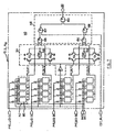
- FIG. 60 the layout of a section of an SDRAM implementing a column redundancy scheme according to a general embodiment of the present invention, is shown by numeral 60. More specifically, the column redundancy scheme illustrated is that for a 256M (Mbit) SDRAM in which the memory chip is divided into four banks, with 16x32 blocks per bank, i.e. 16 blocks of rowlines and 32 blocks of columns. Each bank is physically separated into two half banks in the column direction by row decoders, with each half bank having sixteen (16) column blocks. Each block comprises sixty four (64) normal columns 62 and one (1) redundant column.
- Mbit 16M
- Each bank is physically separated into two half banks in the column direction by row decoders, with each half bank having sixteen (16) column blocks.
- Each block comprises sixty four (64) normal columns 62 and one (1) redundant column.
- the section 60 shown has blocks numbered BLOCK1, BLOCK2, BLOCK3 and BLOCK4, and this layout is repeated four times for a half bank and eight times for an entire bank.
- the redundant column 64 associated with each block is shown at the right hand side thereof.
- Each block has a core Y decoder circuit YDEC 66 (Note: core circuitry refers to circuitry that is physically and functionally associated with the memory array; the terms column and Y are used interchangeably) and a single core redundant decoder RY 68 and driver RYDEC 70.
- the core Y decoders 66 are the second stage of the overall Y decoding for the chip.
- the core Y decoder gets its input from Y- predecoder (not shown) outputs PY and completes the column decoding.
- the first stage of column decoding is performed by the Y predecoders which, from global column address signals ACL[0:8] (not shown), generate the following predecoded Y addresses: PY0_1_2(7:0), PY3_4(3:0), PY5_6(3:0), PY7_8(3:0). All of these addresses are shown generally in Figure 4 as bus PY which carries the predecoded address signals to the core Y decoder 66 and core Y redundancy circuitry 68.
- Y address latch such as Y address latch, burst control, interleave control, sequential burst, interleave burst and Y address prefetch, all well-known in the SDRAM field, are all implemented in the Y predecoder circuit.
- each block has one Y redundancy column 64 and decoder RY 68 located at the side of the block.
- the Y redundancy decoder 70 and its corresponding BLOCK core Y decoder 66 share the same block selection signal (BSEL).
- BSEL block selection signal
- the core Y-decoders 66 and the redundant column 64 are clocked by a common Y select clock signal YSG.
- the overall structure of the four related redundant Y decoders, their relations to the core Y decoders and core-I/Os are illustrated in Figure 4.
- the YSG signals are distributed locally.
- the YSG signal drivers at the center of the bank pass YSG signals throughout an entire bank.
- Local YSG signal distribution circuitry indicated as YSG1, YSG2, YSG3 etc., and shown in detail in figure 9, are provided for each block.
- Each of the local YSG signal distribution circuitry 72 switch and drive the YSG signal to either a normal core Y decoder 66 or to the corresponding Y redundancy decoder 68 in response to the output RDEC from the redundant Y decoder.
- the YSG signal distribution circuitry YSG1, YSG2, YSG3 etc.
- redundancy decoders within adjacent odd or even blocks are shared by all four blocks and can be used to replace any bad normal column within these four blocks.
- the DB_CTL outputs of the redundant Y decoder are connected to a four input AND gate 68b.
- the output RY 10 F 4 from this gate is shared by the four redundancy decoders.
- DB_CTL When a redundant Y decoder is working, its output signal DB_CTL is set low, so RY 10 F 4 is set low to inform the core-I/O circuitry (core data path circuitry) that a redundant Y decoder is being used.
- the BSEL signal goes high.
- the corresponding core-I/O needs to be enabled so core-I/O control signal DBSW_CTL goes high.
- DBSW_CTL goes high. If the selected normal column is bad, it can be replaced by a redundant Y decoder, either within or outside the current block. Under this failure case even if BSEL is still high, whether DBSW_CTL goes high or not depends on the position of the failure replacement.
- the DBSW-CTL signal is responsible for switching the appropriate data bus pass gates 67 for coupling the selected column data to the data bus.
- the RY 10 F 4 , BSEL and DB_CTL which controls the core I/O switch.
- the core-I/O switch rule is shown in the following table: INPUTS OUTPUT RY 10 F 4 BSEL DB_CTL DBSW_CTL 0 0 0 1 1 0 0 1 0 1 0 1 0 1 0 1 1 1 1 1 1
- FIG. 5(a) and 5(b) a schematic diagram of the core Y decoder 66a and a Y driver 66b.
- the combined circuit is shown schematically in block 66 of figure 4.
- the core Y decoder 66a comprises a pair of NAND gates 72 and 74 for receiving the Y predecoder outputs PY0_1_2, PY3_4, PY5_6 and PY7_8.
- the outputs from the NAND gates 72 and 74 are combined in a NOR gate 76 to provide decoded output signal DEC.
- the decoder circuit 66a is equivalent to a four input AND gate.
- the output from the core Y decoder DEC is coupled to the column driver circuit 66b as shown in figure 5(b).
- the normal or redundant column driver 66b receives the Y clock enable signals YSG_B0 and YSG_B1 at respective CMOS pass gates 82 and 84 which are controlled by the output signal DEC in conjunction with signals BUSL and BUSL .
- the clock signals YSG_B0 and YSG_B1 are passed through the CMOS gates at the appropriate time to an inverter 86 which then drives the corresponding column with the signal Y_B0 or Y_B1, depending on the state of the BUSL or the BUSL signals.
- the decoded signal DEC controls the pass gates 82 and 84.
- the overall core Y decoder YDEC 66 shown in figure 4 may be built with the two components shown in figures 5(a) and 5(b). For example, if the Y address has nine bits, it then has 512 different decoding outputs. The even bits and odd bits may be separated to drive four even blocks and four odd blocks respectively. The arrangement will then repeat itself two times to realize a complete core wide decoder for a half bank or four times for a whole bank.
- each memory block has one redundant column located at the side of the block.
- the redundancy decoder RY and its corresponding core Y decoder YDEC share the same block selection signal (BSEL).
- the redundancy decoder RY shown in figure 6 includes a pair of address-compare circuits 92 and 94 which receive the predecoded addresses PY0_1_2, PY3_4, PY5_6 and PY7_8.
- Each address-compare circuit 92 and 94 is capable of being programmed with a single address thus the redundant Y decoder is capable of being programmed to two redundant addresses. Details of the address compare circuitry 92 and 94 will be discussed with reference to figure 7.
- a row address signal AX12 is provided to the redundant Y decoder to perform the upper or lower column portion selection.
- the row address signal AX12 is coupled to the control inputs of a pair of CMOS pass gates 96 and 98 which receive the respective outputs from the address-compare circuits 92 and 94.
- the RY signal is coupled to an inverter 99 to drive the RDEC signal, which in turn drives the column driver 66b shown in figure 5(b) and the YSG signal distribution circuit 72 shown in figure 4.
- the circuit also includes the INI1 and INI0 generation circuitry.
- the circuit comprises a chain of series connected inverters 100 driven from a main INI signal line, and the INI0 and INI1 signals taken as taps along the chain.
- the address compare circuits 92 and 94 of figure 6 are shown in detail. Since the predecoder (figure 4) has four groups of predecoded outputs: PY0_1_2, PY3_4, PY5_6 and PY7_8, the address-compare circuit comprises four groups of programmable fuse circuits 142. Each group of fuse circuits includes four fuses with an associated fuse state evaluation circuit 180 shown in figure 8. The inputs to each of the constituent fuse evaluation circuits in a group are derived from the predecoded column address signals in each group, i.e., PY0_1_2, PY3_4, PY5_6 or PY7_8.
- the outputs PY_OUT from each of the fuses in a group 142 are combined to provide respective signals PY_OUT1, PY_OUT2, PY_OUT3 and PY_OUT4. These signals are passed through an initialization circuit 144 before being combined in an address combiner circuit 146.
- the address combiner circuit is essentially a four input NAND gate which outputs a redundant select signal RY shown in figure 6.
- the operation of the circuit 90 is as follows. If there are no defective columns and no need for redundancy, then no fuse circuits are blown, and the PY_OUT lines are all initialized to a logic low due to the initialization portion 144 of the circuit. This is in contrast with some of the prior art address-compare implementations where fuses of defective addresses were left intact while all fuses of non-defective columns were blown. That approach complicates the redundancy programming process considerably.
- the initialization circuit 144 is comprised of a pair of NOR gates 148 and 150, each connected to receive at its inputs a respective PY_OUT signal. Each of the NOR gate inputs are coupled to a respective NMOS transistor 152 and 154.
- the gates of these transistors are connected to their respective NOR gate output.
- the outputs of the NOR gates are logic high while the feedback connections via the feedback transistors further latch the inputs to logic low.
- the same logic low signals on lines PY_OUT are fed into NAND gates 155 and 156 thus producing logic highs at their outputs.
- the signal CST_BLK is a block redundancy test signal which is normally high, thus enabling NAND gates 157 and 158.
- both outputs from NAND gates 157 and 158 are logic low, which in turn produce a logic high out of NAND gate 160, indicating that redundancy is not being used, i.e., RY is logic high.
- the appropriate predecoder column address is programmed into each of the fuse circuit groups as described earlier.
- the programming signal lines PY_OUT1, PY_OUT2, PY_OUT3 and PY_OUT4 will all be set to logic high upon receipt of the predecoded signals since the address-compare circuit outputs will override the initialization devices; this process will be described in more detail below.
- the circuit 180 receives one of the predecoded address signals on its PY_IN terminal which is in turn connected to a CMOS pass gate 182 formed by a NMOS and PMOS transistor 183 and 184 respectively.
- the output of the CMOS pass gate 182 is the signal PY_OUT.
- the gates of pass gates 183 and 184 are controlled by a fuse element 186.
- the initial conditions for the pass gate 182 are set by a NAND gate 188, which in turn has its initial conditions determined by its inputs received from signals INI0 and INI1.
- the IN and INI1 signals are slightly delayed versions of one another with INI0 preceding INI1, as shown in figure 6.
- a feedback PMOS transistor 190 has its gate connected to output of NAND gate 188 and its drain connected to one of the inputs 188b of the NAND gate 188, forming a half-latch.
- the feedback transistor 190 is used to latch the programmed redundancy address.
- the INI1 signal is applied directly to the other input 188a of the NAND gate 188 and to the gate of an NMOS transistor 192 having its source connected to one end of the fuse 186 the other end of which is connected to ground.
- the drain terminal of the NMOS transistor 192 is connected to the drain terminal of a PMOS transistor 194 which in turn has its source connected to the V DD supply.
- the INI0 signal is applied to the gate of the PMOS transistor 194.
- the common drain connection between the PMOS transistor 194 and the NMOS transistor 192 is connected to the first input 188b of the NAND gate 188.
- the output from the NAND gate 188 is connected via an inverter 196 to drive one of the pass gate transistors 183.
- the fuse state is evaluated as follows. Signal INI0 and INI1 are generated from the POWER_OK signal and INI1 is delayed from INI0. Initially, both INI0 and INI1 are low and the CMOS transmission gate is open and the predecoded signal cannot be passed. In general operation, if the fuse is not blown, once both INI0 and INI1 have become high, the CMOS transmission gate keeps its open state. On the other hand, if the fuse is blown, the CMOS transmission gate is closed and the predecoded signal PY_IN is passed as a redundant predecoded address signal PY_OUT.
- the feedback transistor 190 is used to latch the redundant state of the fuse circuit for the pass gate 182.
- this PMOS device 190 is fairly long to allow easy resetability of the half latch.
- long channel transistors tend to consume more power and take up more area than ones with shorter channels.
- the role of the delayed initialization signals INI0 and INI1 also serves to reduce the size of the feedback transistor 190 to a normal size. This implementation therefore reduces the current consumption during fuse evaluation.
- the delayed activation of the INI0 and INI1 signals avoids a race condition as follows: if INI0 and INI1 were one and the same signal, during the transition from a low to a high, both devices 194 and 192 would be conducting. Since device 194 could achieve a faster pull-up than the pull-down through 192 due to the resistance of the fuse, node 188b would tend to remain high, and once INI1 would be sufficiently high, both inputs to NAND gate 188 would be high, pulling its output low and turning on transistor 190. But while transistor 190 would be turning on, transistor 192 would also be turned on, creating a path from VDD to ground, assuming the fuse is not blown. The race is therefore between the turning on of 194,192 and 190.
- INI1 In contrast, by staggering the transition of INIO and INI1, where INI0 goes from low to high first and then after a delay, INI1 also goes from low to high, the following operation avoids the race condition mentioned above.
- INI0 initially low, device 194 is in the on state as power-up is occurring.
- INI0 goes from low to high, device 194 turns off and node 188b is left to float at high temporarily. Note that due to the fact that INI1 is still low, the output of 188 is still high, and device 190 is in an off state.
- INI1 begins its transition from low to high (no logic transitions can be instantaneous square-wave type transitions in actual operation, there will always be some slight delay resulting in more of a ramp-like transition), transistor 192 begins to turn on and node 188b is easily discharged since there is no contest with device 194.
- INI1 node 188a
- node 188b is going from floating high to low, and therefore, the output of NAND gate 188, as long as the fuse is not blown, will remain high, transistor 190 will not be turned on, and the pass gate 182 will remain off.
- the PY_IN signal will not be passed through the pass gate and the PY_OUT terminal signal will remain at its initialized state as described above.
- the YSG switching circuit 72 (figure 4) is shown in detail.
- the switching circuit includes a pair of YSG latches 200 coupled to latch and delay the input RDEC signal.
- the YSG signal is held for two clock cycles due to the dual data bus architecture.
- the output RYSG_B (1.0) and YSG_B (1.0) are coupled to the redundant driver 70 and the normal Y drivers respectively.
- RCTL (redundant decoder control) output from the latches 200 are coupled to an input of respective gates 202 and 204, while a CTL (decoder control) output is coupled to the inputs of a second pair of NAND gates 206 and 208.
- Both sets of NAND gates 202, 204 and 206, 208 receive the YSG signal on one of their other inputs.
- the YSG latches 200 have their outputs RCTL and CTL of complementary polarity.
- the NAND gates 202, 204 and 206, 208 are responsible for switching the YSG signal to either RYSG_B or YSG_B.
- the number of redundant Y drivers associated with a group of normal Y drivers may be varied.
- the column redundancy system may be applied to all types of RAMs such as DRAMs, SDRAMs, SGRAMs, and the like.
- the redundancy system described herein could also be adapted to implement row redundancy.
Landscapes
- Engineering & Computer Science (AREA)
- Theoretical Computer Science (AREA)
- Physics & Mathematics (AREA)
- General Engineering & Computer Science (AREA)
- General Physics & Mathematics (AREA)
- For Increasing The Reliability Of Semiconductor Memories (AREA)
- Dram (AREA)
- Logic Circuits (AREA)
- Techniques For Improving Reliability Of Storages (AREA)
Abstract
Description
- This invention relates to semiconductor memories and in particular to semiconductor memories having a flexible and efficient circuit for substituting redundant columns for defective columns.
- Semiconductor dynamic random access memories (DRAMs) are typically formed of wordlines and columns crossing the wordlines. Capacitors adjacent each crossing of the rowlines and columns store charge, designating the data to be stored. The capacitors are coupled to the columns by an access transistor in order to receive or discharge charge upon receipt of an appropriate voltage on the rowlines. The rowlines and columns are selected so as to read and write to particular capacitors by means of row (or X) decoders and column (or Y) decoders.
- There are sometimes physical faults associated with the columns or associated elements. For this reason, RAMs usually contain redundant (spare) columns which involve the provision of extra memory elements and column circuitry. The extra memory and required redundant decoders to access that memory in place of defective columns uses valuable semiconductor chip area and decreases the area efficiency of the memory.
- Various techniques have been implemented to provide column redundancy schemes in synchronous dynamic random access memories (SDRAMs). Amongst these are the address compare approach, the address detector approach, the shifter approach, and the address or data steering approach as well as combinations thereof. For example, a first of these techniques utilizes an Y address comparator, wherein pre-decoded Y address signals (PY1:N) pass through fuses to generate redundant column enable signals (RCE) as illustrated in figure 1. The fuses associated with the
redundancy comparator 2 having inherent capacitance and resistance add an extra delay in the Y redundant path. - A second technique shown in figure 2 involves an
Y address detector 4 wherein Y address signals (AY(N-1:0)) control NMOS gates that connect to a pre-charged node through fuses and each can generate redundant column enable signals. When an Y address matches a fuse programming pattern, a column redundant enable signal (COL_RED_EN) is maintained high in order to indicate that the column corresponding to the current Y address will be replaced by a redundant one. Because of this redundancy detecting circuit, timing between the normal and the redundant column path is usually different. Additional logic circuits are required to adjust the timing difference, i.e. a time delay circuit must be employed in the normal address signal path in order to compensate for the slower redundant path. - A further technique known as a shift replacement Y decoder utilizes fuses in the Y decoders but not connected in the signal path. Generally, two Y select lines share one group of fuses. In order to replace a column, the column is disabled by blowing the fuse inside the Y decoder. Shifting the Y driver access for the defective block over to an adjacent driver completes replacement. An advantage of this system is that since fuses are not connected in the column address path, no difference in timing between the normal and redundant path exists. Furthermore, block replacement is possible (failed columns can be repaired in each block with different decoding of each block). A disadvantage of this system is that two adjacent Y select lines must be replaced at the same time making this technique less flexible than other techniques. Furthermore, one directional shifting is required of the columns.
- In figure 3,
redundancy circuitry 10 is implemented which uses an address steering approach according to an embodiment of the invention disclosed in United States Patent Application no. 08/904,153 to Chen et al. assigned to MOSAID Technologies Inc. In this approach, each Y decoder consists of anNMOS multiplexer 12 which steers the column select signal either down the normal or redundant paths according to the information programmed in thefuse circuit 14. NMOS transistors are used in conjunction with an on-chip boosted voltage supply VPP to select the appropriate path since the NMOS transistors in the multiplexer require a voltage larger than VDD to fully turn them on. The redundant select line RYSEL 16 is long and exhibits considerable RC delay. In this implementation two redundant column drivers are accessible by 64 normal columns, but the redundant drivers are dedicated to replacing faulty columns only in that block and can not be used to replace faulty columns in any other blocks within a quadrant. This lack of flexibility proves to be intolerable when moving from the 64M SDRAM density to the 256M SDRAM density. Furthermore, the length of the RYSELline 16 makes such a design too slow for the 256M generation SDRAM. - Thus, it may be seen that there is a need for a redundancy scheme that reduces the timing difference between normal and redundant column paths and which reduces the number of fuses and provides greater flexibility in repairing faulty columns and is capable of accommodating the speed requirements of large memories.
- The invention seeks to provide a column redundancy apparatus and method for a semiconductor memory that allows a redundant column in one memory block to replace a defective column in another memory block and two column defects in a given memory block with a single column redundancy.
- In accordance with one aspect of the invention a semiconductor memory has a plurality of memory blocks, each memory block having memory elements arranged in a plurality of rows and a plurality of columns. The plurality of columns in each memory block include a plurality of normal columns and at least one redundant column. A normal column driver is associated with each normal column. The normal column driver enables access to the associated normal column in response to a decoded memory address signal. A redundant column driver is associated with each redundant column. The redundant column driver enables access to the associated redundant column. A redundant column driver in a first memory block is responsive to a decoded memory address signal indicative of a defective normal column in another memory block.
- In accordance with another aspect of the invention a method is provided for replacing a defective column in a memory block. The memory block is one of a plurality of memory blocks in a semiconductor memory having memory cells arranged in rows and columns, each memory block having a plurality of normal columns and at least one redundant column. A column address corresponding to the location of a defective column in a first memory block is stored. A memory address indicating a normal column to be accessed is received and compared to the stored address and in the event of a match, access to a redundant column in a second memory block is enabled.
- A better understanding of the invention will be obtained by reference to the detailed description below in conjunction with the following drawings in which;
- Figure 1 illustrates a redundancy programming circuit according to the prior art;
- Figure 2 indicates a further redundancy programming circuit according to the prior art;
- Figure 3 is a schematic diagram of a redundancy address steering scheme according to the prior art;
- Figure 4 is a plan view showing a layout for part of a semiconductor memory with a column redundancy scheme according to an embodiment of the present invention;
- Figure 5(a) is a schematic diagram of a normal column decoder according to an embodiment of the present invention;
- Figure 5(b) is a schematic diagram of a column driver according to an embodiment of the present invention;
- Figure 6 is a schematic diagram of a redundant column decoder according to an embodiment of the present invention;
- Figure 7 is a schematic diagram of an address compare circuit according to an embodiment of the present invention;
- Figure 8 is a schematic diagram of a fuse evaluation circuit according to an embodiment of the present invention;
- Figure 9 is a schematic diagram of a column clock distribution circuit according to an embodiment of the present invention; and
- Figure 10 is a schematic diagram of a redundant decoder latch according to an embodiment of the present invention.
-
- In the following description, like numerals refer to similar elements in the drawings. Referring to figure 4, the layout of a section of an SDRAM implementing a column redundancy scheme according to a general embodiment of the present invention, is shown by
numeral 60. More specifically, the column redundancy scheme illustrated is that for a 256M (Mbit) SDRAM in which the memory chip is divided into four banks, with 16x32 blocks per bank, i.e. 16 blocks of rowlines and 32 blocks of columns. Each bank is physically separated into two half banks in the column direction by row decoders, with each half bank having sixteen (16) column blocks. Each block comprises sixty four (64)normal columns 62 and one (1) redundant column. Thesection 60 shown has blocks numbered BLOCK1, BLOCK2, BLOCK3 and BLOCK4, and this layout is repeated four times for a half bank and eight times for an entire bank. Theredundant column 64 associated with each block is shown at the right hand side thereof. Each block has a core Y decoder circuit YDEC 66 (Note: core circuitry refers to circuitry that is physically and functionally associated with the memory array; the terms column and Y are used interchangeably) and a single coreredundant decoder RY 68 anddriver RYDEC 70. Thecore Y decoders 66 are the second stage of the overall Y decoding for the chip. The core Y decoder gets its input from Y- predecoder (not shown) outputs PY and completes the column decoding. The first stage of column decoding is performed by the Y predecoders which, from global column address signals ACL[0:8] (not shown), generate the following predecoded Y addresses: PY0_1_2(7:0), PY3_4(3:0), PY5_6(3:0), PY7_8(3:0). All of these addresses are shown generally in Figure 4 as bus PY which carries the predecoded address signals to thecore Y decoder 66 and coreY redundancy circuitry 68. Logic functions such as Y address latch, burst control, interleave control, sequential burst, interleave burst and Y address prefetch, all well-known in the SDRAM field, are all implemented in the Y predecoder circuit. - As described above, each block has one
Y redundancy column 64 anddecoder RY 68 located at the side of the block. TheY redundancy decoder 70 and its corresponding BLOCKcore Y decoder 66 share the same block selection signal (BSEL). As a result, by changing the block selection signal BSEL, a redundant column in one block can be used to replace a faulty normal column in any adjacent four blocks within a bank, as will be described in further detail below. The core Y-decoders 66 and theredundant column 64 are clocked by a common Y select clock signal YSG. The overall structure of the four related redundant Y decoders, their relations to the core Y decoders and core-I/Os are illustrated in Figure 4. - In this embodiment, the YSG signals are distributed locally. The YSG signal drivers at the center of the bank pass YSG signals throughout an entire bank. Local YSG signal distribution circuitry, indicated as YSG1, YSG2, YSG3 etc., and shown in detail in figure 9, are provided for each block. Each of the local YSG
signal distribution circuitry 72 switch and drive the YSG signal to either a normalcore Y decoder 66 or to the correspondingY redundancy decoder 68 in response to the output RDEC from the redundant Y decoder. The YSG signal distribution circuitry YSG1, YSG2, YSG3 etc. is clocked by BUSL andBUSL signals to latch its corresponding redundant Y decoder output RDEC for 2 clock cycles, as shown in figure 9. If the latched logic value is high, the YSG signals are switched to redundant Y decoder to drive theredundancy column 64. If the latched logic value is low, the YSG signals are switched to core Y decoder to drive the normal column. - Generally, four redundancy decoders within adjacent odd or even blocks are shared by all four blocks and can be used to replace any bad normal column within these four blocks. The
DB_CTL outputs of the redundant Y decoder are connected to a four input ANDgate 68b. The outputRY10F4 from this gate is shared by the four redundancy decoders. Thus when a redundant Y decoder is working, its output signalDB_CTL is set low, soRY10F4 is set low to inform the core-I/O circuitry (core data path circuitry) that a redundant Y decoder is being used. - When a normal column is selected within a block, the BSEL signal goes high. The corresponding core-I/O needs to be enabled so core-I/O control signal DBSW_CTL goes high. If the selected normal column is bad, it can be replaced by a redundant Y decoder, either within or outside the current block. Under this failure case even if BSEL is still high, whether DBSW_CTL goes high or not depends on the position of the failure replacement. The DBSW-CTL signal is responsible for switching the appropriate data
bus pass gates 67 for coupling the selected column data to the data bus. TheRY10F4 , BSEL andDB_CTL , which controls the core I/O switch. The core-I/O switch rule is shown in the following table:INPUTS OUTPUT RY10F4 BSEL DB_CTL DBSW_CTL 0 0 0 1 1 0 0 1 0 1 1 0 1 0 1 0 1 1 1 1 - It may be noted that in the 256M SDRAM embodiment illustrated in figure 5b, there are two versions of all control signals and data buses, one marked as B0 and the other marked as B1. While B0 signals are active, B1 signals are precharging and while B1 signals are active, the B0 signals are precharging. Thus, hiding the precharge time for a higher speed operation. This dual data bus architecture is described in US patent 5,416,743 assigned to MOSAID Technologies, which is hereby incorporated by reference. The BUSL and
BUSL signals schedule the toggling between B0 and B1 signals. - Referring now to figure 5(a) and 5(b), a schematic diagram of the
core Y decoder 66a and aY driver 66b. The combined circuit is shown schematically inblock 66 of figure 4. Thecore Y decoder 66a comprises a pair ofNAND gates NAND gates gate 76 to provide decoded output signal DEC. Thedecoder circuit 66a is equivalent to a four input AND gate. The output from the core Y decoder DEC is coupled to thecolumn driver circuit 66b as shown in figure 5(b). - The normal or
redundant column driver 66b, receives the Y clock enable signalsYSG_B0 andYSG_B1 at respectiveCMOS pass gates BUSL . The clock signalsYSG_B0 andYSG_B1 are passed through the CMOS gates at the appropriate time to aninverter 86 which then drives the corresponding column with the signal Y_B0 or Y_B1, depending on the state of the BUSL or theBUSL signals. Thus, the decoded signal DEC controls thepass gates - The overall core
Y decoder YDEC 66 shown in figure 4 may be built with the two components shown in figures 5(a) and 5(b). For example, if the Y address has nine bits, it then has 512 different decoding outputs. The even bits and odd bits may be separated to drive four even blocks and four odd blocks respectively. The arrangement will then repeat itself two times to realize a complete core wide decoder for a half bank or four times for a whole bank. - Turning back to figure 6, a detailed diagram of the
redundancy decoder RY 68 of figure 4 is shown. The redundant Y decoders RY1, RY2, ... RYN are used to determine if access to a redundant column is required. These redundant Y decoders utilize an address-compare scheme to make this determination. To reiterate, each memory block has one redundant column located at the side of the block. The redundancy decoder RY and its corresponding core Y decoder YDEC share the same block selection signal (BSEL). The redundancy decoder RY shown in figure 6 includes a pair of address-comparecircuits circuit circuitry - Because normal columns may have separately addressed upper or lower portions within a block, a row address signal AX12 is provided to the redundant Y decoder to perform the upper or lower column portion selection. The row address signal AX12 is coupled to the control inputs of a pair of
CMOS pass gates circuits RY signal is coupled to aninverter 99 to drive the RDEC signal, which in turn drives thecolumn driver 66b shown in figure 5(b) and the YSGsignal distribution circuit 72 shown in figure 4. - The circuit also includes the INI1 and INI0 generation circuitry. Generally the circuit comprises a chain of series connected
inverters 100 driven from a main INI signal line, and the INI0 and INI1 signals taken as taps along the chain. - Referring now to figure 7, the address compare
circuits programmable fuse circuits 142. Each group of fuse circuits includes four fuses with an associated fusestate evaluation circuit 180 shown in figure 8. The inputs to each of the constituent fuse evaluation circuits in a group are derived from the predecoded column address signals in each group, i.e., PY0_1_2, PY3_4, PY5_6 or PY7_8. The outputs PY_OUT from each of the fuses in agroup 142 are combined to provide respective signals PY_OUT1, PY_OUT2, PY_OUT3 and PY_OUT4. These signals are passed through an initialization circuit 144 before being combined in anaddress combiner circuit 146. The address combiner circuit is essentially a four input NAND gate which outputs a redundant select signalRY shown in figure 6. Each of these circuit sections will now be discussed in detail. - The operation of the circuit 90 is as follows. If there are no defective columns and no need for redundancy, then no fuse circuits are blown, and the PY_OUT lines are all initialized to a logic low due to the initialization portion 144 of the circuit. This is in contrast with some of the prior art address-compare implementations where fuses of defective addresses were left intact while all fuses of non-defective columns were blown. That approach complicates the redundancy programming process considerably. The initialization circuit 144 is comprised of a pair of NOR
gates respective NMOS transistor NAND gates NAND gates NAND gate NAND gates NAND gate 160, indicating that redundancy is not being used, i.e.,RY is logic high. - If a faulty location is detected during testing, then the appropriate predecoder column address is programmed into each of the fuse circuit groups as described earlier. As a result, the programming signal lines PY_OUT1, PY_OUT2, PY_OUT3 and PY_OUT4 will all be set to logic high upon receipt of the predecoded signals since the address-compare circuit outputs will override the initialization devices; this process will be described in more detail below. Consequently, with two logic high inputs applied to the
NAND gates NAND gates NAND gate 160, which in turn provides the active low output signalRY , indicating the use of redundancy. It is important to note that in the embodiment of the present invention, firstly if no defective address is detected, no fuses need to be blown, whereas in the prior art address compare approach of figure 1, all fuses would have to be blown. Secondly, if a defective address is detected, to program a defective address, in the present invention embodiment no more than four (4) fuses must be blown compared to twelve (12) fuses for the prior art address-compare scheme. These differences represent a substantial simplification of the redundancy programming function. - Referring to figure 8, a detailed schematic of the fuse
state evaluation circuit 180 of figure 7 is shown. As described above, thecircuit 180 receives one of the predecoded address signals on its PY_IN terminal which is in turn connected to aCMOS pass gate 182 formed by a NMOS andPMOS transistor CMOS pass gate 182 is the signal PY_OUT. The gates ofpass gates fuse element 186. The initial conditions for thepass gate 182 are set by aNAND gate 188, which in turn has its initial conditions determined by its inputs received from signals INI0 and INI1. The IN and INI1 signals are slightly delayed versions of one another with INI0 preceding INI1, as shown in figure 6. - A
feedback PMOS transistor 190 has its gate connected to output ofNAND gate 188 and its drain connected to one of theinputs 188b of theNAND gate 188, forming a half-latch. Thefeedback transistor 190 is used to latch the programmed redundancy address. The INI1 signal is applied directly to theother input 188a of theNAND gate 188 and to the gate of anNMOS transistor 192 having its source connected to one end of thefuse 186 the other end of which is connected to ground. The drain terminal of theNMOS transistor 192 is connected to the drain terminal of aPMOS transistor 194 which in turn has its source connected to the VDD supply. The INI0 signal is applied to the gate of thePMOS transistor 194. The common drain connection between thePMOS transistor 194 and theNMOS transistor 192 is connected to thefirst input 188b of theNAND gate 188. The output from theNAND gate 188 is connected via aninverter 196 to drive one of thepass gate transistors 183. - The fuse state is evaluated as follows. Signal INI0 and INI1 are generated from the POWER_OK signal and INI1 is delayed from INI0. Initially, both INI0 and INI1 are low and the CMOS transmission gate is open and the predecoded signal cannot be passed. In general operation, if the fuse is not blown, once both INI0 and INI1 have become high, the CMOS transmission gate keeps its open state. On the other hand, if the fuse is blown, the CMOS transmission gate is closed and the predecoded signal PY_IN is passed as a redundant predecoded address signal PY_OUT.
- As previously mentioned with reference to figure 6, there is a delay between the transition of signals INI0 and INI1. The delay of INI1 from INI0 ensures that there is no DC current flowing from the supply voltage VDD through the
fuse 186 to ground when the fuse is intact. As mentioned above, thefeedback transistor 190 is used to latch the redundant state of the fuse circuit for thepass gate 182. Typically, in prior art circuits thisPMOS device 190 is fairly long to allow easy resetability of the half latch. However, long channel transistors tend to consume more power and take up more area than ones with shorter channels. The role of the delayed initialization signals INI0 and INI1 also serves to reduce the size of thefeedback transistor 190 to a normal size. This implementation therefore reduces the current consumption during fuse evaluation. Furthermore, the delayed activation of the INI0 and INI1 signals avoids a race condition as follows: if INI0 and INI1 were one and the same signal, during the transition from a low to a high, bothdevices device 194 could achieve a faster pull-up than the pull-down through 192 due to the resistance of the fuse,node 188b would tend to remain high, and once INI1 would be sufficiently high, both inputs toNAND gate 188 would be high, pulling its output low and turning ontransistor 190. But whiletransistor 190 would be turning on,transistor 192 would also be turned on, creating a path from VDD to ground, assuming the fuse is not blown. The race is therefore between the turning on of 194,192 and 190. In contrast, by staggering the transition of INIO and INI1, where INI0 goes from low to high first and then after a delay, INI1 also goes from low to high, the following operation avoids the race condition mentioned above. With INI0 initially low,device 194 is in the on state as power-up is occurring. As INI0 goes from low to high,device 194 turns off andnode 188b is left to float at high temporarily. Note that due to the fact that INI1 is still low, the output of 188 is still high, anddevice 190 is in an off state. As INI1 begins its transition from low to high (no logic transitions can be instantaneous square-wave type transitions in actual operation, there will always be some slight delay resulting in more of a ramp-like transition),transistor 192 begins to turn on andnode 188b is easily discharged since there is no contest withdevice 194. The result is that as INI1 (node 188a) is going from low to high,node 188b is going from floating high to low, and therefore, the output ofNAND gate 188, as long as the fuse is not blown, will remain high,transistor 190 will not be turned on, and thepass gate 182 will remain off. As a result, the PY_IN signal will not be passed through the pass gate and the PY_OUT terminal signal will remain at its initialized state as described above. - If the
fuse 186 is blown, then theinput 188b ofNAND gate 188 is not pulled to a logic low level. As a result, bothinput NAND gate 188 are at a logic high, resulting in a logic low output from the NAND gate. This logic low output is latched through the turning on oftransistor 190 and enables theCMOS pass gate 182. As a result, for redundant operation (with the fuse blown), thepass gate 182 allows the signal PY_IN to pass through as signal PY_OUT and override the precharge value on the corresponding precharge line shown in figure 7. It is important to note that only fuses of faulty addresses need to be blown and not those of non-defective addresses. - Referring to figure 9, the YSG switching circuit 72 (figure 4) is shown in detail. The switching circuit includes a pair of YSG latches 200 coupled to latch and delay the input RDEC signal. The YSG signal is held for two clock cycles due to the dual data bus architecture. The output
RYSG_B(1.0) andYSG_B(1.0) are coupled to theredundant driver 70 and the normal Y drivers respectively. RCTL (redundant decoder control) output from thelatches 200 are coupled to an input ofrespective gates NAND gates NAND gates NAND gates - While the invention has been described in connection with the specific embodiment thereof, and in a specific use, various modifications thereof will occur to those skilled in the art without departing from the spirit of the invention as set forth in the appended claims. For example, the number of redundant Y drivers associated with a group of normal Y drivers may be varied. Furthermore, the column redundancy system may be applied to all types of RAMs such as DRAMs, SDRAMs, SGRAMs, and the like. Similarly, by making well-known amendments to the circuitry, the redundancy system described herein could also be adapted to implement row redundancy.
- The terms and expressions which have been employed in this specification are used as terms of description and not of limitations, there is no intention in the use of such terms and expressions to exclude any equivalence of the features shown and described or portions thereof, but it is recognized that various modifications are possible within the scope of the claims to the invention.
Claims (28)
- A semiconductor memory comprising:a plurality of memory blocks, each memory block having memory elements arranged in a plurality of rows and a plurality of columns, the plurality of columns in each memory block including a plurality of normal columns and at least one redundant column;a normal column driver associated with each normal column, the normal column driver for enabling access to the associated normal column in response to a decoded normal memory address signal;a redundant column driver associated with each redundant column, the redundant column driver for enabling access to the associated redundant column in response to a redundant column memory address signal;a redundant column decoder generating the redundant column memory address signal in response to at least one column memory address signal and to a portion selection signal.
- A semiconductor memory in accordance with claim 1, wherein the redundant column driver in a first memory block is also responsive to a decoded memory address signal indicative of a defective normal column in the first memory block.
- A semiconductor memory in accordance with claim 2, wherein the plurality of memory blocks comprise an upper and a lower portion respectively and each redundant column driver is adapted to separately enable access to the upper and lower portions of the associated redundant column.
- A semiconductor memory in accordance with claim 3, wherein the redundant column driver enables a first portion of the redundant column to be addressed in response to the portion selection signal.
- A semiconductor memory in accordance with claim 3, wherein a first portion selection signal is indicative of a defect in the upper portion of a first normal column address and a second portion selection signal is indicative of a defect in the lower portion of a second normal column address.
- A semiconductor memory in accordance with claim 3, wherein a first defect in a first column address is replaced by a first portion of a first redundant column and a second defect in a second column address is replaced by a second portion of the first redundant column.
- A semiconductor memory in accordance with claim 3, wherein a first defect in an upper portion of a first normal column address is replaced by an upper portion of a first redundant column, and a second defect in a lower portion of a second column address is replaced by a lower portion of the first redundant column.
- A semiconductor memory in accordance with claim 3, wherein a first defect in an upper portion of a first normal column address in a first memory block is replaced by an upper portion of a first redundant column, and a second defect in a lower portion of a second column address in the first memory block is replaced by a lower portion of the first redundant column, the first redundant column located in the first memory block.
- A semiconductor memory in accordance with claim 3, wherein a first defect in an upper portion of a first normal column address in a first memory block is replaced by an upper portion of a first redundant column, and a second defect in a lower portion of a second column address in the first memory block is replaced by a lower portion of the first redundant column, the first redundant column located in a second memory block.
- A semiconductor memory in accordance with claim 3, wherein a first defect in an upper portion of a first normal column address in a first memory block is replaced by an upper portion of a first redundant column in a first memory block, and a second defect in a lower portion of a second column address in the first memory block is replaced by a lower portion of a second redundant column, the second redundant column located in a second memory block.
- A semiconductor memory in accordance with claim 1, wherein for each block, the decoded memory address signal is provided by a normal address decoder and the decoded memory address signal indicative of a defective normal column is provided by a redundant address decoder.
- A semiconductor memory in accordance with claim 11, wherein the redundant address decoder comprises an address-compare circuit for comparing the memory address signal with a column address corresponding to the location of a defective column.
- A semiconductor memory in accordance with claim 12, comprising a programmable fuse bank for storing the column address corresponding to the location of the defective column.
- A semiconductor memory in accordance with claim 12, comprising an output circuit for asserting a signal indicative of a match between the memory address signal and the column address corresponding to the location of a defective column.
- A semiconductor memory in accordance with claim 14, further comprising a switch responsive to the signal indicative of a match, the switch being operative to selectively couple a clock signal to a normal column driver or a redundant column driver.
- A semiconductor memory in accordance with claim 1, comprising a data pass gate for each redundant column, the data pass gate responsive to a data path control signal to pass data from an enabled redundant column to a common data bus.
- A method for replacing a defective column in a memory block, the memory block being one of a plurality of memory blocks in a semiconductor memory having memory cells arranged in rows and columns, each memory block having a plurality of normal columns and at least one redundant column, the method comprising the steps of:storing a column address corresponding to the location of a defective column in a first memory block;receiving a memory address indicating at least a normal column to be accessed;comparing the memory address to the stored column address and in the event of a match, enabling access to a redundant column in a second memory block.
- A method according to claim 17, wherein the received memory address indicates a normal column to be accessed in one of the plurality of memory blocks.
- A method according to claim 17, wherein the plurality of memory blocks are separated into upper and lower portions and comprising the further step of decoding the received memory address to indicate which portion of the upper and lower portions is to be enabled for access.
- A method according to claim 17, wherein storing a column address comprises blowing a plurality of fuses corresponding to the column address of the defective column.
- A method according to claim 17, comprising the step of enabling access to the plurality of memory blocks by asserting a block select signal.
- A method according to claim 17, comprising the further step of generating data path control signals for selectively coupling an enabled redundant column to a data bus.
- A method for replacing a defective portion in a column in a memory block, the memory block being one of a plurality of memory blocks in a semiconductor memory having memory cells arranged in rows and columns, each memory block having a plurality of normal columns and at least one redundant column, the method comprising the steps of:storing a column address and a portion selection signal corresponding to the location of a defective column portion;receiving a memory address indicating at least a normal column to be accessed;comparing the memory address to the stored column address and in the event of a match, replacing a portion indicated by the stored portion selection signal in the normal column with a portion, in particular a corresponding portion, in the redundant column.
- A method according to claim 23, wherein the received memory address indicates a normal column to be accessed in one of the plurality of memory blocks.
- A method according to claim 23, wherein the plurality of memory blocks are separated into upper and lower portions and comprising the further step of decoding the received memory address to indicate which portion of the upper and lower portions is to be enabled for access.
- A method according to claim 23, wherein storing a column address comprises blowing a plurality of fuses corresponding to the column address of the column having the defective portion and the portion selection signal corresponding to the defective portion.
- A method according to claim 23, comprising the step of enabling access to the plurality of memory blocks by asserting a block select signal.
- A method according to claim 23, comprising the further step of generating data path control signals for selectively coupling an enabled redundant column to a data bus.
Applications Claiming Priority (3)
| Application Number | Priority Date | Filing Date | Title |
|---|---|---|---|
| US182495 | 1994-01-18 | ||
| US09/182,495 US6137735A (en) | 1998-10-30 | 1998-10-30 | Column redundancy circuit with reduced signal path delay |
| EP99953491A EP1125203B1 (en) | 1998-10-30 | 1999-10-29 | Column redundancy circuit with reduced signal path delay |
Related Parent Applications (1)
| Application Number | Title | Priority Date | Filing Date |
|---|---|---|---|
| EP99953491A Division EP1125203B1 (en) | 1998-10-30 | 1999-10-29 | Column redundancy circuit with reduced signal path delay |
Publications (4)
| Publication Number | Publication Date |
|---|---|
| EP1526458A2 true EP1526458A2 (en) | 2005-04-27 |
| EP1526458A3 EP1526458A3 (en) | 2006-03-29 |
| EP1526458B1 EP1526458B1 (en) | 2008-10-08 |
| EP1526458B8 EP1526458B8 (en) | 2008-12-24 |
Family
ID=22668727
Family Applications (2)
| Application Number | Title | Priority Date | Filing Date |
|---|---|---|---|
| EP99953491A Expired - Lifetime EP1125203B1 (en) | 1998-10-30 | 1999-10-29 | Column redundancy circuit with reduced signal path delay |
| EP04023097A Expired - Lifetime EP1526458B8 (en) | 1998-10-30 | 1999-10-29 | Column redundancy circuit with reduced signal path delay |
Family Applications Before (1)
| Application Number | Title | Priority Date | Filing Date |
|---|---|---|---|
| EP99953491A Expired - Lifetime EP1125203B1 (en) | 1998-10-30 | 1999-10-29 | Column redundancy circuit with reduced signal path delay |
Country Status (10)
| Country | Link |
|---|---|
| US (1) | US6137735A (en) |
| EP (2) | EP1125203B1 (en) |
| JP (1) | JP4965025B2 (en) |
| KR (1) | KR100724816B1 (en) |
| CN (1) | CN1186725C (en) |
| AT (1) | ATE278217T1 (en) |
| AU (1) | AU1024500A (en) |
| CA (1) | CA2347765C (en) |
| DE (2) | DE69939716D1 (en) |
| WO (1) | WO2000026784A1 (en) |
Families Citing this family (10)
| Publication number | Priority date | Publication date | Assignee | Title |
|---|---|---|---|---|
| KR100363085B1 (en) * | 1999-11-05 | 2002-12-05 | 삼성전자 주식회사 | Semiconductor memory device having row redundancy scheme for improving redundancy efficiency |
| JP2002050191A (en) * | 2000-08-02 | 2002-02-15 | Fujitsu Ltd | Semiconductor memory |
| US6775759B2 (en) * | 2001-12-07 | 2004-08-10 | Micron Technology, Inc. | Sequential nibble burst ordering for data |
| US20040015645A1 (en) * | 2002-07-19 | 2004-01-22 | Dodd James M. | System, apparatus, and method for a flexible DRAM architecture |
| US6674673B1 (en) | 2002-08-26 | 2004-01-06 | International Business Machines Corporation | Column redundancy system and method for a micro-cell embedded DRAM (e-DRAM) architecture |
| CN100593215C (en) * | 2004-02-20 | 2010-03-03 | 斯班逊有限公司 | Semiconductor storage device and semiconductor storage device control method |
| US7035152B1 (en) * | 2004-10-14 | 2006-04-25 | Micron Technology, Inc. | System and method for redundancy memory decoding |
| US7251173B2 (en) * | 2005-08-02 | 2007-07-31 | Micron Technology, Inc. | Combination column redundancy system for a memory array |
| CN105355233B (en) * | 2015-11-23 | 2018-04-10 | 清华大学 | Efficient data wiring method based on PCM reversion error correction algorithms |
| CN107389211B (en) * | 2017-06-29 | 2019-03-12 | 西安邮电大学 | A kind of binary code turns thermometer-code circuit |
Citations (3)
| Publication number | Priority date | Publication date | Assignee | Title |
|---|---|---|---|---|
| EP0559368A2 (en) * | 1992-03-02 | 1993-09-08 | Motorola, Inc. | Memory column redundancy and localized column redundancy control signals |
| US5270975A (en) * | 1990-03-29 | 1993-12-14 | Texas Instruments Incorporated | Memory device having a non-uniform redundancy decoder arrangement |
| US5894441A (en) * | 1997-03-31 | 1999-04-13 | Nec Corporation | Semiconductor memory device with redundancy circuit |
Family Cites Families (14)
| Publication number | Priority date | Publication date | Assignee | Title |
|---|---|---|---|---|
| US4598388A (en) * | 1985-01-22 | 1986-07-01 | Texas Instruments Incorporated | Semiconductor memory with redundant column circuitry |
| JP2564507B2 (en) * | 1985-04-16 | 1996-12-18 | 富士通株式会社 | Semiconductor memory device |
| JPH01125799A (en) * | 1987-11-11 | 1989-05-18 | Fujitsu Ltd | Semiconductor memory device |
| DE69132951T2 (en) * | 1991-08-28 | 2002-09-12 | Oki Electric Ind Co Ltd | SEMICONDUCTOR STORAGE DEVICE |
| US5257229A (en) * | 1992-01-31 | 1993-10-26 | Sgs-Thomson Microelectronics, Inc. | Column redundancy architecture for a read/write memory |
| DE59409008D1 (en) * | 1994-08-12 | 2000-01-20 | Siemens Ag | Redundancy circuit arrangement for an integrated semiconductor memory |
| KR0130030B1 (en) * | 1994-08-25 | 1998-10-01 | 김광호 | Column redundancy circuit and method for semiconductor memory device |
| US5572470A (en) * | 1995-05-10 | 1996-11-05 | Sgs-Thomson Microelectronics, Inc. | Apparatus and method for mapping a redundant memory column to a defective memory column |
| JPH0955080A (en) * | 1995-08-08 | 1997-02-25 | Fujitsu Ltd | Semiconductor storage device and method for writing in and reading out cell information for the same device |
| EP0758112B1 (en) * | 1995-08-09 | 2002-07-03 | Infineon Technologies AG | Integrated semiconductor memory device having redundancy circuit arrangement |
| US5646896A (en) * | 1995-10-31 | 1997-07-08 | Hyundai Electronics America | Memory device with reduced number of fuses |
| US5732030A (en) * | 1996-06-25 | 1998-03-24 | Texas Instruments Incorporated | Method and system for reduced column redundancy using a dual column select |
| CA2202692C (en) * | 1997-04-14 | 2006-06-13 | Mosaid Technologies Incorporated | Column redundancy in semiconductor memories |
| KR100281284B1 (en) * | 1998-06-29 | 2001-02-01 | 김영환 | Column redundancy circuit |
-
1998
- 1998-10-30 US US09/182,495 patent/US6137735A/en not_active Expired - Lifetime
-
1999
- 1999-10-29 KR KR1020017005435A patent/KR100724816B1/en not_active IP Right Cessation
- 1999-10-29 DE DE69939716T patent/DE69939716D1/en not_active Expired - Lifetime
- 1999-10-29 WO PCT/CA1999/001054 patent/WO2000026784A1/en active IP Right Grant
- 1999-10-29 EP EP99953491A patent/EP1125203B1/en not_active Expired - Lifetime
- 1999-10-29 EP EP04023097A patent/EP1526458B8/en not_active Expired - Lifetime
- 1999-10-29 CN CNB998128104A patent/CN1186725C/en not_active Expired - Lifetime
- 1999-10-29 AT AT99953491T patent/ATE278217T1/en not_active IP Right Cessation
- 1999-10-29 DE DE69920735T patent/DE69920735T2/en not_active Expired - Lifetime
- 1999-10-29 JP JP2000580093A patent/JP4965025B2/en not_active Expired - Fee Related
- 1999-10-29 AU AU10245/00A patent/AU1024500A/en not_active Abandoned
- 1999-10-29 CA CA002347765A patent/CA2347765C/en not_active Expired - Fee Related
Patent Citations (3)
| Publication number | Priority date | Publication date | Assignee | Title |
|---|---|---|---|---|
| US5270975A (en) * | 1990-03-29 | 1993-12-14 | Texas Instruments Incorporated | Memory device having a non-uniform redundancy decoder arrangement |
| EP0559368A2 (en) * | 1992-03-02 | 1993-09-08 | Motorola, Inc. | Memory column redundancy and localized column redundancy control signals |
| US5894441A (en) * | 1997-03-31 | 1999-04-13 | Nec Corporation | Semiconductor memory device with redundancy circuit |
Also Published As
| Publication number | Publication date |
|---|---|
| EP1526458B1 (en) | 2008-10-08 |
| KR100724816B1 (en) | 2007-06-04 |
| US6137735A (en) | 2000-10-24 |
| DE69920735D1 (en) | 2004-11-04 |
| DE69920735T2 (en) | 2005-02-10 |
| DE69939716D1 (en) | 2008-11-20 |
| EP1526458A3 (en) | 2006-03-29 |
| CN1331818A (en) | 2002-01-16 |
| WO2000026784A1 (en) | 2000-05-11 |
| ATE278217T1 (en) | 2004-10-15 |
| AU1024500A (en) | 2000-05-22 |
| CN1186725C (en) | 2005-01-26 |
| KR20010085983A (en) | 2001-09-07 |
| JP4965025B2 (en) | 2012-07-04 |
| EP1526458B8 (en) | 2008-12-24 |
| CA2347765C (en) | 2008-07-29 |
| CA2347765A1 (en) | 2000-05-11 |
| EP1125203A1 (en) | 2001-08-22 |
| EP1125203B1 (en) | 2004-09-29 |
| JP2002529874A (en) | 2002-09-10 |
Similar Documents
| Publication | Publication Date | Title |
|---|---|---|
| US6084818A (en) | Semiconductor memory device capable of efficient memory cell select operation with reduced element count | |
| US6272056B1 (en) | Semiconductor memory device capable of implementing redundancy-based repair efficiently in relation to layout and operating speed and semiconductor integrated circuit device having such semiconductor memory device | |
| US5796662A (en) | Integrated circuit chip with a wide I/O memory array and redundant data lines | |
| US6519192B2 (en) | Semiconductor memory device having a large band width and allowing efficient execution of redundant repair | |
| CA2389986C (en) | Architecture with multi-instance redundancy implementation | |
| KR100790442B1 (en) | Memory device with global redundancy and its operating method | |
| US5469401A (en) | Column redundancy scheme for DRAM using normal and redundant column decoders programmed with defective array address and defective column address | |
| US5963489A (en) | Method and apparatus for redundancy word line replacement in a repairable semiconductor memory device | |
| JP4519208B2 (en) | Semiconductor memory device | |
| US5544113A (en) | Random access memory having a flexible array redundancy scheme | |
| KR19980063434A (en) | Row redundancy block architecture | |
| US6144591A (en) | Redundancy selection circuit for semiconductor memories | |
| CA2202692C (en) | Column redundancy in semiconductor memories | |
| EP1526458B1 (en) | Column redundancy circuit with reduced signal path delay | |
| US6058052A (en) | Redundancy scheme providing improvements in redundant circuit access time and integrated circuit layout area | |
| KR20000022718A (en) | Sub-block redundancy replacement for a giga-bit scale dram | |
| US6335897B1 (en) | Semiconductor memory device including redundancy circuit adopting latch cell | |
| US6320801B1 (en) | Redundancy circuit and redundancy method for semiconductor memory device | |
| US20080068905A1 (en) | Reparable semiconductor memory device | |
| US20240029781A1 (en) | Apparatuses and methods for repairing mutliple bit lines with a same column select value | |
| US6928008B2 (en) | Semiconductor memory devices with data line redundancy schemes and method therefore | |
| CA2246763C (en) | Improved redundancy selection circuit for semiconductor memories | |
| JPH09106697A (en) | Semiconductor memory device |
Legal Events
| Date | Code | Title | Description |
|---|---|---|---|
| PUAI | Public reference made under article 153(3) epc to a published international application that has entered the european phase |
Free format text: ORIGINAL CODE: 0009012 |
|
| AC | Divisional application: reference to earlier application |
Ref document number: 1125203 Country of ref document: EP Kind code of ref document: P |
|
| AK | Designated contracting states |
Kind code of ref document: A2 Designated state(s): AT BE CH CY DE DK ES FI FR GB GR IE IT LI LU MC NL PT SE |
|
| PUAL | Search report despatched |
Free format text: ORIGINAL CODE: 0009013 |
|
| AK | Designated contracting states |
Kind code of ref document: A3 Designated state(s): AT BE CH CY DE DK ES FI FR GB GR IE IT LI LU MC NL PT SE |
|
| RIC1 | Information provided on ipc code assigned before grant |
Ipc: G11C 29/00 20060101AFI20060203BHEP |
|
| 17P | Request for examination filed |
Effective date: 20060920 |
|
| 17Q | First examination report despatched |
Effective date: 20061016 |
|
| AKX | Designation fees paid |
Designated state(s): DE FI FR GB IT NL |
|
| GRAP | Despatch of communication of intention to grant a patent |
Free format text: ORIGINAL CODE: EPIDOSNIGR1 |
|
| GRAS | Grant fee paid |
Free format text: ORIGINAL CODE: EPIDOSNIGR3 |
|
| GRAA | (expected) grant |
Free format text: ORIGINAL CODE: 0009210 |
|
| AC | Divisional application: reference to earlier application |
Ref document number: 1125203 Country of ref document: EP Kind code of ref document: P |
|
| AK | Designated contracting states |
Kind code of ref document: B1 Designated state(s): DE FI FR GB IT NL |
|
| REG | Reference to a national code |
Ref country code: GB Ref legal event code: FG4D |
|
| RAP2 | Party data changed (patent owner data changed or rights of a patent transferred) |
Owner name: MOSAID TECHNOLOGIES INCORPORATED Owner name: PANASONIC CORPORATION |
|
| REF | Corresponds to: |
Ref document number: 69939716 Country of ref document: DE Date of ref document: 20081120 Kind code of ref document: P |
|
| NLT2 | Nl: modifications (of names), taken from the european patent patent bulletin |
Owner name: MOSAID TECHNOLOGIES INCORPORATED EN PANASONIC CORP Effective date: 20081119 |
|
| PLBE | No opposition filed within time limit |
Free format text: ORIGINAL CODE: 0009261 |
|
| STAA | Information on the status of an ep patent application or granted ep patent |
Free format text: STATUS: NO OPPOSITION FILED WITHIN TIME LIMIT |
|
| PG25 | Lapsed in a contracting state [announced via postgrant information from national office to epo] |
Ref country code: IT Free format text: LAPSE BECAUSE OF FAILURE TO SUBMIT A TRANSLATION OF THE DESCRIPTION OR TO PAY THE FEE WITHIN THE PRESCRIBED TIME-LIMIT Effective date: 20081008 |
|
| 26N | No opposition filed |
Effective date: 20090709 |
|
| REG | Reference to a national code |
Ref country code: FR Ref legal event code: CA |
|
| REG | Reference to a national code |
Ref country code: DE Ref legal event code: R082 Ref document number: 69939716 Country of ref document: DE Representative=s name: 24IP LAW GROUP SONNENBERG FORTMANN, DE |
|
| REG | Reference to a national code |
Ref country code: FR Ref legal event code: CA Effective date: 20141021 Ref country code: FR Ref legal event code: CD Owner name: CONVERSANT INTELLECTUAL PROPERTY MANAGEMENT IN, CA Effective date: 20141021 |
|
| REG | Reference to a national code |
Ref country code: DE Ref legal event code: R081 Ref document number: 69939716 Country of ref document: DE Owner name: PANASONIC CORPORATION, KADOMA-SHI, JP Free format text: FORMER OWNER: MOSAID TECHNOLOGIES INC., PANASONIC CORPORATION, , JP Effective date: 20141120 Ref country code: DE Ref legal event code: R082 Ref document number: 69939716 Country of ref document: DE Representative=s name: 24IP LAW GROUP SONNENBERG FORTMANN, DE Effective date: 20141120 Ref country code: DE Ref legal event code: R081 Ref document number: 69939716 Country of ref document: DE Owner name: CONVERSANT INTELLECTUAL PROPERTY MANAGEMENT IN, CA Free format text: FORMER OWNER: MOSAID TECHNOLOGIES INC., PANASONIC CORPORATION, , JP Effective date: 20141120 Ref country code: DE Ref legal event code: R081 Ref document number: 69939716 Country of ref document: DE Owner name: PANASONIC CORPORATION, KADOMA-SHI, JP Free format text: FORMER OWNERS: MOSAID TECHNOLOGIES INC., OTTAWA, ONTARIO, CA; PANASONIC CORPORATION, KADOMA-SHI, OSAKA, JP Effective date: 20141120 Ref country code: DE Ref legal event code: R081 Ref document number: 69939716 Country of ref document: DE Owner name: CONVERSANT INTELLECTUAL PROPERTY MANAGEMENT IN, CA Free format text: FORMER OWNERS: MOSAID TECHNOLOGIES INC., OTTAWA, ONTARIO, CA; PANASONIC CORPORATION, KADOMA-SHI, OSAKA, JP Effective date: 20141120 |
|
| REG | Reference to a national code |
Ref country code: NL Ref legal event code: TD Effective date: 20150216 |
|
| REG | Reference to a national code |
Ref country code: FR Ref legal event code: PLFP Year of fee payment: 17 |
|
| PGFP | Annual fee paid to national office [announced via postgrant information from national office to epo] |
Ref country code: GB Payment date: 20151019 Year of fee payment: 17 Ref country code: FI Payment date: 20151020 Year of fee payment: 17 |
|
| PGFP | Annual fee paid to national office [announced via postgrant information from national office to epo] |
Ref country code: FR Payment date: 20151029 Year of fee payment: 17 Ref country code: NL Payment date: 20151029 Year of fee payment: 17 |
|
| PGFP | Annual fee paid to national office [announced via postgrant information from national office to epo] |
Ref country code: DE Payment date: 20161214 Year of fee payment: 18 |
|
| REG | Reference to a national code |
Ref country code: NL Ref legal event code: MM Effective date: 20161101 |
|
| GBPC | Gb: european patent ceased through non-payment of renewal fee |
Effective date: 20161029 |
|
| REG | Reference to a national code |
Ref country code: FR Ref legal event code: ST Effective date: 20170630 |
|
| PG25 | Lapsed in a contracting state [announced via postgrant information from national office to epo] |
Ref country code: FI Free format text: LAPSE BECAUSE OF NON-PAYMENT OF DUE FEES Effective date: 20161029 Ref country code: FR Free format text: LAPSE BECAUSE OF NON-PAYMENT OF DUE FEES Effective date: 20161102 Ref country code: GB Free format text: LAPSE BECAUSE OF NON-PAYMENT OF DUE FEES Effective date: 20161029 |
|
| PG25 | Lapsed in a contracting state [announced via postgrant information from national office to epo] |
Ref country code: NL Free format text: LAPSE BECAUSE OF NON-PAYMENT OF DUE FEES Effective date: 20161101 |
|
| REG | Reference to a national code |
Ref country code: DE Ref legal event code: R119 Ref document number: 69939716 Country of ref document: DE |
|
| PG25 | Lapsed in a contracting state [announced via postgrant information from national office to epo] |
Ref country code: DE Free format text: LAPSE BECAUSE OF NON-PAYMENT OF DUE FEES Effective date: 20180501 |