JP4959080B2 - Reflective mask substrate coating - Google Patents
Reflective mask substrate coating Download PDFInfo
- Publication number
- JP4959080B2 JP4959080B2 JP2001501941A JP2001501941A JP4959080B2 JP 4959080 B2 JP4959080 B2 JP 4959080B2 JP 2001501941 A JP2001501941 A JP 2001501941A JP 2001501941 A JP2001501941 A JP 2001501941A JP 4959080 B2 JP4959080 B2 JP 4959080B2
- Authority
- JP
- Japan
- Prior art keywords
- layer
- substrate
- silicon
- surface side
- mask substrate
- Prior art date
- Legal status (The legal status is an assumption and is not a legal conclusion. Google has not performed a legal analysis and makes no representation as to the accuracy of the status listed.)
- Expired - Lifetime
Links
Images


Classifications
-
- B—PERFORMING OPERATIONS; TRANSPORTING
- B82—NANOTECHNOLOGY
- B82Y—SPECIFIC USES OR APPLICATIONS OF NANOSTRUCTURES; MEASUREMENT OR ANALYSIS OF NANOSTRUCTURES; MANUFACTURE OR TREATMENT OF NANOSTRUCTURES
- B82Y10/00—Nanotechnology for information processing, storage or transmission, e.g. quantum computing or single electron logic
-
- B—PERFORMING OPERATIONS; TRANSPORTING
- B82—NANOTECHNOLOGY
- B82Y—SPECIFIC USES OR APPLICATIONS OF NANOSTRUCTURES; MEASUREMENT OR ANALYSIS OF NANOSTRUCTURES; MANUFACTURE OR TREATMENT OF NANOSTRUCTURES
- B82Y40/00—Manufacture or treatment of nanostructures
-
- G—PHYSICS
- G03—PHOTOGRAPHY; CINEMATOGRAPHY; ANALOGOUS TECHNIQUES USING WAVES OTHER THAN OPTICAL WAVES; ELECTROGRAPHY; HOLOGRAPHY
- G03F—PHOTOMECHANICAL PRODUCTION OF TEXTURED OR PATTERNED SURFACES, e.g. FOR PRINTING, FOR PROCESSING OF SEMICONDUCTOR DEVICES; MATERIALS THEREFOR; ORIGINALS THEREFOR; APPARATUS SPECIALLY ADAPTED THEREFOR
- G03F1/00—Originals for photomechanical production of textured or patterned surfaces, e.g., masks, photo-masks, reticles; Mask blanks or pellicles therefor; Containers specially adapted therefor; Preparation thereof
- G03F1/22—Masks or mask blanks for imaging by radiation of 100nm or shorter wavelength, e.g. X-ray masks, extreme ultraviolet [EUV] masks; Preparation thereof
- G03F1/24—Reflection masks; Preparation thereof
-
- G—PHYSICS
- G03—PHOTOGRAPHY; CINEMATOGRAPHY; ANALOGOUS TECHNIQUES USING WAVES OTHER THAN OPTICAL WAVES; ELECTROGRAPHY; HOLOGRAPHY
- G03F—PHOTOMECHANICAL PRODUCTION OF TEXTURED OR PATTERNED SURFACES, e.g. FOR PRINTING, FOR PROCESSING OF SEMICONDUCTOR DEVICES; MATERIALS THEREFOR; ORIGINALS THEREFOR; APPARATUS SPECIALLY ADAPTED THEREFOR
- G03F1/00—Originals for photomechanical production of textured or patterned surfaces, e.g., masks, photo-masks, reticles; Mask blanks or pellicles therefor; Containers specially adapted therefor; Preparation thereof
- G03F1/38—Masks having auxiliary features, e.g. special coatings or marks for alignment or testing; Preparation thereof
- G03F1/46—Antireflective coatings
-
- H—ELECTRICITY
- H10—SEMICONDUCTOR DEVICES; ELECTRIC SOLID-STATE DEVICES NOT OTHERWISE PROVIDED FOR
- H10P—GENERIC PROCESSES OR APPARATUS FOR THE MANUFACTURE OR TREATMENT OF DEVICES COVERED BY CLASS H10
- H10P76/00—Manufacture or treatment of masks on semiconductor bodies, e.g. by lithography or photolithography
- H10P76/40—Manufacture or treatment of masks on semiconductor bodies, e.g. by lithography or photolithography of masks comprising inorganic materials
- H10P76/408—Manufacture or treatment of masks on semiconductor bodies, e.g. by lithography or photolithography of masks comprising inorganic materials characterised by their sizes, orientations, dispositions, behaviours or shapes
- H10P76/4085—Manufacture or treatment of masks on semiconductor bodies, e.g. by lithography or photolithography of masks comprising inorganic materials characterised by their sizes, orientations, dispositions, behaviours or shapes characterised by the processes involved to create the masks
-
- G—PHYSICS
- G21—NUCLEAR PHYSICS; NUCLEAR ENGINEERING
- G21K—HANDLING OF PARTICLES OR IONISING RADIATION NOT OTHERWISE PROVIDED FOR; IRRADIATION DEVICES; GAMMA RAY OR X-RAY MICROSCOPES
- G21K2201/00—Arrangements for handling radiation or particles
- G21K2201/06—Arrangements for handling radiation or particles using diffractive, refractive or reflecting elements
- G21K2201/067—Construction details
Landscapes
- Engineering & Computer Science (AREA)
- Physics & Mathematics (AREA)
- General Physics & Mathematics (AREA)
- Chemical & Material Sciences (AREA)
- Nanotechnology (AREA)
- Crystallography & Structural Chemistry (AREA)
- Mathematical Physics (AREA)
- Theoretical Computer Science (AREA)
- Condensed Matter Physics & Semiconductors (AREA)
- Manufacturing & Machinery (AREA)
- Preparing Plates And Mask In Photomechanical Process (AREA)
- Exposure Of Semiconductors, Excluding Electron Or Ion Beam Exposure (AREA)
Description
【0001】
米国政府は、Lawrence Livermore National Laboratoryの事業に関する米国エネルギー省とカリフォルニア大学との契約No.W‐7405‐ENG‐48に従い、この発明に権利を有している。
【0002】
【関連出願】
この出願は6/7/99付で出願されたUS仮出願60/138,158およびそのクレイム優先権と関連している。
【0003】
【発明の背景】
本発明はリソグラフィー用の反射マスク基板、具体的には極紫外線リソグラフィー用の反射マスク基板、更に具体的には、マスク基板として低熱膨張性物質の使用を可能にして、このような基板で多層膜応力作用を相殺するコーティングをマスク基板の表面(フロント)および/または裏面(バック)へ施すこと、追加コーティングがマスク基板の表面(フロント)および/または裏面(バック)へ適用されることに関する。
【0004】
極紫外線リソグラフィー(EUVL)は、半導体マイクロエレクトロニクスを加工する次世代リソグラフィーシステム用の筆頭候補である。EUVLと従来のリソグラフィーとの主要な差異は、EUVLが13.4nm光を用いるため、多層膜(ML)、典型的にはMo/Siでコートされた反射光素子およびマスクを要することである。欠陥を容易に精査しうる低熱膨張性物質(LTEM)透明マスク基板の開発は、現在発展中の重要な面である。
【0005】
EUVリソグラフィーマスクまたはレチクルの熱管理は、極紫外線リソグラフィー(EUVL)システムに関する現在の開発努力からみて重要な分野になっている。S.E.Gianoulakis et al.,”Thermal-mechanical performance of extreme ultraviolet lithographic rectiles”,J.Vac.Sci.Technol.B16(6)3440-3,Nov./Dec.1998およびS.E.Gianoulakis et al.,”Thermal management of EUV lithographymasks using low expansion glass substrates”,Emerging Lithographic Technologies III,SPIE Proceedings,Vol.3676,1999参照。
【0006】
現在、epi-Si(100)ウェハが、少ない欠陥、優れた平面性および仕上げ並びに精査および超清浄取扱い機器の存在のようなそれらの望ましい性質のおかげで、EUVLマスクブランク用の基板として用いられている。しかしながら、シリコンは許容し得ないほど大きな熱膨張率を有している。印刷中に、EUV光の〜40%はマスクに吸収されてしまい、加熱により生じた熱膨張は大きな画像たわみを引き起こして、エラー・バジェット(error budget)を超えることがある。低熱膨張性物質(LTEM)はEUVLマスク用の基板物質として提案されてきた。W.M.Tong et al.,”Mask substrated requirements and development for extreme ultraviolet lithography(EUVL)” ,SPIE,Vol.3873,Sept.1999参照。しかしながら、LTEM基板の使用には次の面で新たな挑戦を克服する必要がある。
【0007】
1.精査
欠陥数はEUVLマスク加工にとり主要な関心事であり、欠陥精査は欠陥を減らす上で重要なステップである。光散乱が最新の欠陥精査機器で用いられている。欠陥の散乱断面積は可視波長で反射性の表面により高められる:ULEのような透明LTEM基板で最少の検出可能な欠陥サイズ検知閾値(〜0.12μm)はシリコン表面の場合(〜60nm)よりも高い。透明基板で欠陥検知を高める手段が必要とされる。
【0008】
2.表面仕上げ
EUVLマスクでは、画像配置エラーおよび反射能の喪失を最少に抑えるために、低い平面性エラーおよび低い面粗性を各々要求する。平面性および面粗性の要件を果たす上で役立ついかなる方法も望ましい。
【0009】
3.欠陥
現在、非シリコン基板の欠陥数はシリコンウェハよりもかなり多いが、シリコンウェハで欠陥を少なくという半導体産業の要望が欠陥を減らす上でシリコン基板製造業者に何十億ドルもの投資を余儀なくさせていたからである。最新の欠陥精査、クリーニングおよび他の欠陥減少プロセスを行う現行機器とより適合しうるようにLTEM基板を作ることが高度に望ましい。
【0010】
4.静電マスクチャック
マスクの静電チャッキングはEUVLマスク加工の様々な段階で必要とされている。多層膜コーティングに際する静電チャッキングは機械的チャッキングよりもマスクへ加える欠陥が少ないことが証明された。更に、静電チャッキングはマスクのパターン化、精査および暴露に際してマスクをマウントする上で評価をうけている2つのオプションのうち1つである。しかしながら、ほとんどのLTEMはシリコンと異なり低い誘電率を有しており、同様のチャッキング力を得る上でかなり高い電圧を要する。高電圧は可能性としてプロセッシングステップを妨げる電界を生み出すか、または真空中で絶縁破壊を生じることがある。LTEM基板は低電圧静電チャックと適合するよう作製されねばならない。
【0011】
5.応力バランシング
どのような種類のコーティングを有する基板も、2者間の応力アンバランスのせいでたわむことがある。EUVLマスクの場合、基板はほぼゼロの膨張であって、シリコンのような典型的コーティングが大きさで大抵1または2程度高いCTEを有していることから、この問題は特に激しい。応力形成で1つの可能なメカニズムは次のとおりである:LTEM基板へのML付着は約70℃で行われる。付着後、温度は環境に戻って、MLは収縮する。LTEM基板は収縮しないため、これは応力アンバランスを生じて、たわんだ基板をもたらす。応力アンバランスによるこのたわみを克服するための技術は必須である。
【0012】
本発明は上記の問題に対する解決法を提供するもので、EUVLマスク用の基板物質として低熱膨張性物質(LTEM)の使用を可能とする。本発明では基本的にLTEM基板の表面および/または裏面表面へコーティングを施す。表面コーティングは基板の欠陥精査、欠陥減少、表面仕上げおよび応力バランスを高めるが、裏面コーティングは基板の静電チャッキングおよび応力バランスを高める。
【0013】
【発明の要旨】
フォトリソグラフィー用のマスク基板として低熱膨張性物質の使用を可能とさせることが、本発明の目的である。
本発明の別な目的は、透明でもまたはそうでなくてもよい、低熱膨張性物質から構成されているEUVLマスク基板を加工するために、シリコン、金属または多層膜のようなコーティングを用いるプロセスを提供することである。
本発明のもう1つの目的は、改善された欠陥精査を行えるように、シリコンのようなコーティングを有した透明または非反射性低熱膨張性物質マスク基板を提供することである。
本発明のもう1つの目的は、改善された表面仕上げを行えるように、平滑化効果をもつおよび/または研磨しうる表面コーティングを有したマスク基板を提供することである。
本発明のもう1つの目的は、表面欠陥の減少を行えるように、シリコンおよびモリブデンのような表面コーティングを有したマスク基板を提供することである。
本発明のもう1つの目的は、基板の静電チャッキングを促すために、シリコン、モリブデン、クロム、オキシ窒化クロムまたはTaSiのような、基板よりも高い誘電率の物質の裏面コーティングを有したマスク基板を提供することである。
本発明のもう1つの目的は、コーティングがシリコン、モリブデン、クロム、オキシ窒化クロム、TaSiおよびMo/Si多層膜スタックのような物質を含有している、基板の応力誘導性たわみを直すために、表面および/または裏面にコーティングを有したマスク基板を提供することである。
【0014】
本発明の他の目的および利点は、以下の記載および添付した図面から明らかになるであろう。基本的に、本発明では表面、裏面および/または双方においてコーティングでマスク基板をコートする。マスクの表面におけるコーティングは、欠陥精査を高め、表面仕上げを改善し、欠陥レベルを減らし、および/または他のコーティングとマスク基板との応力アンバランスによる基板のたわみを直すためである。基板の裏面における高誘電性コーティングは、静電チャッキングを促し、欠陥精査を高め、および/またはマスク基板の表面における付着シリコン層および/またはMLコーティングで生じた応力アンバランスによる基板のたわみを直すためである。更に詳しくは、本発明は、表面側でシリコンのような物質でコートされ、裏面側で金属のような少くとも高誘電性のコーティングでコートされた、低熱膨張性物質(LTEM)基板から構成されている、マスク基板に関する。LTEMの片側または両側におけるシリコンコーティングは、欠陥精査、表面仕上げおよび欠陥レベルが改善された透明EUVLマスク基板を供する。基板の裏面側における、付加コーティングおよび高誘電率を有するコーティングは、静電チャッキングを促して、マスク基板の表面側で多層膜コーティングに付着するシリコン層で生じた応力アンバランスによる基板のたわみを直すためにある。加えて、LTEM基板の表面側とシリコンコーティングとの中間またはシリコンコーティングと多層膜との間に、非晶質でもよい膜を形成することは、応力バランスをとる上で役立つ。本発明の透明マスク基板は、EUVLマスク応用に加えて、集積回路製造用の半導体ダイをパターン化する上で他のリソグラフィーシステムにも応用できる。
【0015】
【発明の具体的な説明】
本発明は、EUVLシステムで利用されるような反射マスク基板を用いるフォトリソグラフィー向けに、低熱膨張性物質(LTEM)マスク基板のようなマスク基板上における、シリコンおよび金属コーティングのようなコーティングの使用に関する。本発明では、欠陥精査、表面仕上げおよび欠陥レベルを改善するために、LTEMマスク基板の片側または両側に1以上のコーティングを施し;静電チャッキングを促して、マスク基板の表面側および/または裏面側に付着されたシリコン層または多層膜コーティングで生じた応力アンバランスによるたわみを直すために、基板の裏面側に導電性コーティングを施す。付着コーティングはシリコン、モリブデン、クロム、オキシ窒化クロム、TaSiまたはSi/Mo多層膜から構成しうる。しかも、TaSiのような物質の非晶質膜は、応力バランスをとるために、LTEMとSi膜との間にはさむことができる。低熱膨張性物質は熱膨張率<1ppm/Kの物質として規定され、選択されたガラス、ガラス‐セラミック、プラスチック、セラミック、複合材などから構成しうる。LTEMの例には、Schott Glass Technologies,Duryea,PA製のZerodur;Corning,Inc.,Corning,NY製のULE;Ohara Corp.,相模原,日本製のClearCeram;SiC、石英およびドライシリカがある。ここで記載されているマスクの表面または表面側とは、パターン化される側である。
【0016】
少くとも1つの表面側上層および/または1つの裏面側物質でLTEM基板をコーティングすると、先に記載され、後でも個別に記載されて、表1でまとめられた問題を解決しうる。
【0017】
1.精査:シリコンのような反射コーティングを有する透明または半透明マスク基板は、今日の最新シリコン欠陥精査機器で欠陥精査を行える。これらの機器の精査の感度および速度は、非反射基板を精査する対応機器の場合よりも現在はかなり高い。
【0018】
2.表面仕上げ:シリコン上層ではシリコン産業の成熟した仕上げ力を利用しうる。非晶質、多結晶質またはその他である1〜5μmシリコンのコーティングは、シリコンウェハと同程度の平面性および低面粗性になるまで研磨および加工することができる。これはシリコンウェハと同じように仕上げを行える手法をマスク基板へもたらす。
【0019】
3.欠陥減少:表面コーティングを有する利点は3倍である:第一に、そのコーティングはLTEM基板自体よりもきれいにしやすい物質から作製しうる。例えば、シリコンの表面コーティングを有したマスク基板では、シリコンウェハ用に開発された現行の洗練されたクリーニングテクノロジーおよびプロセスを利用しうる。第二に、シリコンまたはクロムのようなコーティングは、最新の低欠陥プロセス装置で用いられる自動操作装置でセンサーに用いられている可視光に対して基板を不透明にさせうる。そのため、本プロセッシング機器との適合性は有意に高められる。第三に、基板上のいかなる汚染物もオーバーコートで覆われるため、それらはプロセス機器に入れず、それらの機器で行われる他のプロセスを損なうことがない。更に、シリコン基板を仕上げる技術水準がより発達したおかげで、シリコンの表面コーティングは元のLTEM基板表面よりも良い仕上げおよびクリーン度となるまで容易に再研磨しうる。
【0020】
4.静電チャック:静電チャックはパターン化、精査および暴露のためにマスク基板をマウントする上で提案されており、その使用は高誘電率の基板物質により促されるであろう。ほとんどのマスク基板物質、例えばLTEMおよび石英は低い誘電率を有している。限定されないが、シリコン、TiN、モリブデン、クロム、TaSiおよび/またはMo/Si MLスタックを含めた、基板の裏面側における高誘電率のコーティングは、静電チャックの使用を促すようになる。
【0021】
5.応力バランシング:裏面側のコーティングも表面でMLによるたわみを直すために用いうる。裏面コーティングの厚さは、基板とその他のコーティングとの応力アンバランスを直すために必要とされるものに依存する。シリコン、モリブデン、クロム、オキシ窒化クロム、TaSiまたはMo/Si MLスタックのコーティングが用いうる。特に、応力がアニーリングにより調整しうるTaSiおよびオキシ窒化クロムのようなコーティングは、個別マスクの応力バランシングニーズを満たすように仕上げることもできる。
【0022】

ここで図面を参考にしてみると、図1は全体として10で示された従来型EUVLマスク基板の態様を表わしており、LTEMのマスク基板11、例えばMo/Siのような多層膜12、二酸化ケイ素のようなマスクパターン修復用の緩衝層13、並びにTiNおよびCrのような吸収体パターン14から構成されている。
【0024】
図2〜4は、図1の場合と類似しているが、図1の基板11の表面、裏面または両側に1以上の物質層を付着させた、EUVLマスク基板の態様を表わしている。図1の場合に相当する部分は対応した参照番号で示されている。図2において、EUVLマスク基板20は図1のように基板11、多層膜12、緩衝層13および吸収体パターン14からなるが、欠陥精査、応力バランス、欠陥平滑性を高めておよび/または再研磨するために、基板11と多層膜12との間に表面コーティング21を付加している。表面コーティング21はSi、Mo、Cr、オキシ窒化クロム、TaSiまたはMo/Si多層膜のような物質から構成されている。
【0025】
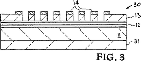
図3は、図1のように基板11、多層膜12、緩衝層13および吸収体パターン14からなるが、静電チャッキングおよび/または応力バランスを促す裏面コーティング31を基板11に付加した、EUVLマスク基板30について示している。裏面コーティング31はSi、Mo、Cr、オキシ窒化クロム、TaSiまたはMo/Si多層膜のような物質から構成されている。
【0026】
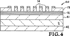
図4は、図1のように基板11、多層膜12、緩衝層13および吸収体パターン14からなるが、図2のように基板11と多層膜12との間に表面コーティング41、および図3のように基板11に裏面コーティング42を付加した、EUVLマスク基板40について示しており、こうすると表面コーティング41は図2のように欠陥精査、応力バランス、欠陥平滑性を高めておよび/または再研磨しうるようになり、裏面コーティング42は図3のように静電チャッキングおよび/または応力バランスを促す。コーティング41および42は各々Si、Mo、Cr、オキシ窒化クロム、TaSiまたはMo/Si多層膜のような物質から構成されうる。
【0027】
表面コーティングおよび21および41と裏面コーティング31および42は単層コーティングとして示されているが、各コーティングは単層および/または多層構造でもよい。
【0028】
本発明は、集積回路製造用の半導体ダイをパターン化するEUVLシステムまたは他のリソグラフィーシステムのように、マスク基板の形成で精査、表面仕上げ、欠陥、応力バランシングおよび静電チャック保持に伴う以前の問題に対する解決法を提供していることが、こうして示された。欠陥精査を高め、表面仕上げを改善して、欠陥を減らし、静電チャッキングを促し、および/または応力アンバランスを直すために、マスク基板表面の表面および/または裏面でコーティングの適用により、本発明はフォトリソグラフィーマスク加工技術の水準をかなり発達させている。
【0029】
低熱膨張性物質を利用するマスク基板の具体的態様が、本発明の原理を例示および記載するために、特定の物質およびパラメーターと共に説明および記載されてきたが、このようなことは制限するためではない。修正および変更は当業者に明らかとなるであろうが、本発明が添付された請求の範囲のみに限定されるわけではない。
【図面の簡単な説明】
添付図面は本開示に組み込まれてその一部を形成するものであって、本発明の態様を図解しており、その記載と一緒にすると本発明の原理を説明する上で役立つ。
【図1】 従来のEUVLマスク基板の態様の横断面図である。
【図2】 本発明に従い作製された、1以上の表面コーティングを有するEUVLマスク基板の態様を示している。
【図3】 本発明に従い1以上の裏面コーティングを有するEUVLマスク基板の態様を示している。
【図4】 本発明に従い1以上の表面コーティングおよび1以上の裏面コーティングを有するEUVLマスク基板の態様を示している。[0001]
The US government has signed a contract with the US Department of Energy and the University of California for Lawrence Livermore National Laboratory. We have the rights to this invention in accordance with W-7405-ENG-48.
[0002]
[Related Applications]
This application is related to US Provisional Application 60 / 138,158 filed 6/7/99 and its claim priority.
[0003]
BACKGROUND OF THE INVENTION
The present invention relates to a reflective mask substrate for lithography, specifically to a reflective mask substrate for extreme ultraviolet lithography, and more specifically to the use of a low thermal expansion material as a mask substrate. It relates to applying a coating that counteracts the stress action to the front (front) and / or back (back) of the mask substrate, and to applying an additional coating to the front (front) and / or back (back) of the mask substrate.
[0004]
Extreme ultraviolet lithography (EUVL) is a leading candidate for next generation lithography systems that process semiconductor microelectronics. The main difference between EUVL and conventional lithography is that since EUVL uses 13.4 nm light, it requires a multilayer (ML), reflective light element and mask, typically coated with Mo / Si. The development of a low thermal expansion material (LTEM) transparent mask substrate that can be easily scrutinized for defects is an important aspect currently under development.
[0005]
Thermal management of EUV lithography masks or reticles has become an important area in view of current development efforts for extreme ultraviolet lithography (EUVL) systems. SEGianoulakis et al., “Thermal-mechanical performance of extreme ultraviolet lithographic rectiles”, J. Vac. Sci. Technol. B16 (6) 3440-3, Nov./Dec. 1998 and SEGianoulakis et al., “Thermal management of EUV lithographymasks using low expansion glass substrates ”, Emerging Lithographic Technologies III, SPIE Proceedings, Vol. 3676, 1999.
[0006]
Currently, epi-Si (100) wafers are used as substrates for EUVL mask blanks because of their desirable properties such as few defects, excellent flatness and finish and the presence of inspection and ultra-clean handling equipment. Yes. However, silicon has an unacceptably large coefficient of thermal expansion. During printing, ˜40% of EUV light is absorbed by the mask, and thermal expansion caused by heating can cause large image deflections, which can exceed the error budget. Low thermal expansion materials (LTEM) have been proposed as substrate materials for EUVL masks. See WMTong et al., “Mask substrated requirements and development for extreme ultraviolet lithography (EUVL)”, SPIE, Vol.3873, Sept.1999. However, the use of the LTEM substrate needs to overcome new challenges in the following aspects.
[0007]
1. The number of inspection defects is a major concern for EUVL mask processing, and defect inspection is an important step in reducing defects. Light scattering is used in modern defect inspection equipment. The scattering cross-section of defects is enhanced by a reflective surface at visible wavelengths: the minimum detectable defect size detection threshold (˜0.12 μm) for transparent LTEM substrates such as ULE is better than for silicon surfaces (˜60 nm) Is also expensive. There is a need for a means to enhance defect detection with a transparent substrate.
[0008]
2. Surface finish EUVL masks require low planarity errors and low surface roughness, respectively, to minimize image placement errors and loss of reflectivity. Any method that helps to meet the planarity and surface roughness requirements is desirable.
[0009]
3. Defects Currently, the number of defects on non-silicon substrates is much higher than on silicon wafers, but the demand from the semiconductor industry to reduce defects on silicon wafers has forced billions of dollars to invest in silicon substrate manufacturers to reduce defects. It is. It is highly desirable to make an LTEM substrate so that it is more compatible with current equipment that performs state-of-the-art defect review, cleaning and other defect reduction processes.
[0010]
4). Electrostatic chuck chucking Electrostatic chucking of the mask is required at various stages of EUVL mask processing. Electrostatic chucking during multilayer coating has proven to have fewer defects on the mask than mechanical chucking. In addition, electrostatic chucking is one of two options that are being evaluated for mask mounting during mask patterning, inspection, and exposure. However, most LTEMs, unlike silicon, have a low dielectric constant and require a fairly high voltage to obtain a similar chucking force. High voltages can potentially create an electric field that interferes with the processing step, or can cause breakdown in a vacuum. The LTEM substrate must be made compatible with the low voltage electrostatic chuck.
[0011]
5. Stress Balancing A substrate with any type of coating can bend due to stress imbalance between the two. In the case of EUVL masks, this problem is particularly acute because the substrate has a nearly zero expansion and a typical coating such as silicon has a CTE that is typically about 1 or 2 higher in size. One possible mechanism for stress formation is as follows: ML deposition on the LTEM substrate takes place at about 70 ° C. After deposition, the temperature returns to the environment and the ML shrinks. Since the LTEM substrate does not shrink, this creates a stress imbalance resulting in a deflected substrate. Techniques for overcoming this deflection due to stress imbalance are essential.
[0012]
The present invention provides a solution to the above problem and allows the use of a low thermal expansion material (LTEM) as a substrate material for EUVL masks. In the present invention, coating is basically applied to the surface and / or the back surface of the LTEM substrate. The surface coating enhances substrate defect inspection, defect reduction, surface finish and stress balance, while the back coating enhances substrate electrostatic chucking and stress balance.
[0013]
SUMMARY OF THE INVENTION
It is an object of the present invention to allow the use of a low thermal expansion material as a mask substrate for photolithography.
Another object of the present invention is a process using coatings such as silicon, metal or multilayers to process EUVL mask substrates composed of low thermal expansion materials, which may or may not be transparent. Is to provide.
Another object of the present invention is to provide a transparent or non-reflective low thermal expansion material mask substrate with a coating such as silicon so that improved defect inspection can be performed.
Another object of the present invention is to provide a mask substrate having a surface coating that has a smoothing effect and / or can be polished so as to provide an improved surface finish.
Another object of the present invention is to provide a mask substrate having a surface coating such as silicon and molybdenum so that surface defects can be reduced.
Another object of the present invention is a mask having a back coating of a material with a higher dielectric constant than the substrate, such as silicon, molybdenum, chromium, chromium oxynitride or TaSi, to facilitate electrostatic chucking of the substrate. It is to provide a substrate.
Another object of the present invention is to correct the stress-induced deflection of the substrate where the coating contains materials such as silicon, molybdenum, chromium, chromium oxynitride, TaSi and Mo / Si multilayer stacks. It is to provide a mask substrate having a coating on the front and / or back.
[0014]
Other objects and advantages of the present invention will become apparent from the following description and accompanying drawings. Basically, the present invention coats the mask substrate with a coating on the front surface, back surface and / or both. The coating on the surface of the mask is to enhance defect inspection, improve surface finish, reduce defect levels, and / or correct substrate deflection due to stress imbalance between other coatings and the mask substrate. High dielectric coating on the backside of the substrate facilitates electrostatic chucking, enhances defect probing, and / or corrects substrate deflection due to stress imbalance caused by deposited silicon layer and / or ML coating on the surface of the mask substrate Because. More particularly, the present invention consists of a low thermal expansion material (LTEM) substrate coated with a material such as silicon on the front side and coated with at least a high dielectric coating such as metal on the back side. The present invention relates to a mask substrate. The silicon coating on one or both sides of the LTEM provides a transparent EUVL mask substrate with improved defect inspection, surface finish and defect level. Additional coatings and high dielectric constant coatings on the back side of the substrate promote electrostatic chucking and reduce the substrate deflection due to stress imbalance caused by the silicon layer adhering to the multilayer coating on the front side of the mask substrate. There is to fix. In addition, forming a film that may be amorphous between the surface side of the LTEM substrate and the silicon coating or between the silicon coating and the multilayer film helps to balance the stress. In addition to EUVL mask applications, the transparent mask substrate of the present invention can be applied to other lithography systems for patterning semiconductor dies for integrated circuit manufacturing.
[0015]
DETAILED DESCRIPTION OF THE INVENTION
The present invention relates to the use of coatings such as silicon and metal coatings on a mask substrate such as a low thermal expansion material (LTEM) mask substrate for photolithography using a reflective mask substrate such as utilized in EUVL systems. . In the present invention, one or more coatings are applied to one or both sides of the LTEM mask substrate to improve defect inspection, surface finish, and defect levels; to facilitate electrostatic chucking and to provide the front side and / or back side of the mask substrate A conductive coating is applied to the back side of the substrate to correct the deflection due to stress imbalance caused by the silicon layer or multilayer coating applied to the side. The adhesion coating may consist of silicon, molybdenum, chromium, chromium oxynitride, TaSi or Si / Mo multilayers. Moreover, an amorphous film of a material such as TaSi can be sandwiched between the LTEM and the Si film in order to balance the stress. The low thermal expansion material is defined as a material having a coefficient of thermal expansion <1 ppm / K, and may be composed of selected glass, glass-ceramic, plastic, ceramic, composite, and the like. Examples of LTEMs include Zerodur from Schott Glass Technologies, Duryea, PA; ULE from Corning, Inc., Corning, NY; ClearCeram from Ohara Corp., Sagamihara, Japan; SiC, quartz and dry silica. The surface or surface side of the mask described here is the side to be patterned.
[0016]
Coating the LTEM substrate with at least one front side top layer and / or one back side material can solve the problems described above and later described individually and summarized in Table 1.
[0017]
1. Probing: Transparent or translucent mask substrates with reflective coatings such as silicon can be probed for defects with today's latest silicon defect inspection equipment. The sensitivity and speed of scrutiny of these instruments is now significantly higher than that of corresponding instruments that scrutinize non-reflective substrates.
[0018]
2. Surface finish: The silicon top layer can take advantage of the mature finishing power of the silicon industry. A coating of 1-5 μm silicon that is amorphous, polycrystalline or otherwise can be polished and processed until it is as planar and low surface roughness as a silicon wafer. This provides the mask substrate with a technique that can be finished in the same way as a silicon wafer.
[0019]
3. Defect reduction: The advantage of having a surface coating is three times: First, the coating can be made from a material that is easier to clean than the LTEM substrate itself. For example, a mask substrate having a surface coating of silicon can utilize current sophisticated cleaning technologies and processes developed for silicon wafers. Secondly, coatings such as silicon or chrome can make the substrate opaque to the visible light used in sensors in automated handling equipment used in modern low defect process equipment. Therefore, the compatibility with the present processing device is significantly improved. Third, because any contaminants on the substrate are covered with the overcoat, they do not enter the process equipment and do not compromise other processes performed on those equipment. Furthermore, thanks to the more advanced state of the art of finishing silicon substrates, silicon surface coatings can be easily repolished to a better finish and cleanliness than the original LTEM substrate surface.
[0020]
4). Electrostatic chucks: Electrostatic chucks have been proposed for mounting mask substrates for patterning, probing and exposure, and their use will be facilitated by high dielectric constant substrate materials. Most mask substrate materials, such as LTEM and quartz, have a low dielectric constant. High dielectric constant coatings on the back side of the substrate, including but not limited to silicon, TiN, molybdenum, chromium, TaSi and / or Mo / Si ML stacks, will encourage the use of electrostatic chucks.
[0021]
5. Stress balancing: A coating on the back side can also be used to correct the ML deflection on the surface. The thickness of the backside coating depends on what is needed to correct the stress imbalance between the substrate and the other coatings. A coating of silicon, molybdenum, chromium, chromium oxynitride, TaSi or Mo / Si ML stacks can be used. In particular, coatings such as TaSi and chromium oxynitride, whose stress can be adjusted by annealing, can also be finished to meet the stress balancing needs of individual masks.
[0022]
Referring now to the drawings, FIG. 1 shows an embodiment of a conventional EUVL mask substrate shown generally as 10, which is an
[0024]
2-4 are similar to those of FIG. 1, but represent an embodiment of the EUVL mask substrate with one or more material layers deposited on the front, back or both sides of the
[0025]
FIG. 3 shows an EUVL comprising a
[0026]
4 includes the
[0027]
Although the
[0028]
The present invention addresses previous problems associated with probing, surface finishing, defects, stress balancing and electrostatic chuck retention in the formation of mask substrates, such as EUVL systems or other lithography systems that pattern semiconductor dies for integrated circuit manufacturing. It has thus been shown that it provides a solution to. By applying a coating on the front and / or back side of the mask substrate surface to improve defect inspection, improve surface finish, reduce defects, promote electrostatic chucking, and / or correct stress imbalance, The invention has considerably advanced the level of photolithographic mask processing technology.
[0029]
While specific embodiments of mask substrates utilizing low thermal expansion materials have been described and described with specific materials and parameters to illustrate and describe the principles of the present invention, such limitations are not intended. Absent. Modifications and changes will become apparent to those skilled in the art, but the invention is not limited to the scope of the appended claims.
[Brief description of the drawings]
The accompanying drawings, which are incorporated in and form a part of this disclosure, illustrate embodiments of the invention and together with the description serve to explain the principles of the invention.
FIG. 1 is a cross-sectional view of an embodiment of a conventional EUVL mask substrate.
FIG. 2 illustrates an embodiment of an EUVL mask substrate having one or more surface coatings made in accordance with the present invention.
FIG. 3 illustrates an embodiment of an EUVL mask substrate having one or more backside coatings in accordance with the present invention.
FIG. 4 illustrates an embodiment of an EUVL mask substrate having one or more surface coatings and one or more backside coatings in accordance with the present invention.
Claims (20)
前記単層基板の表面側に少なくとも一つの物質層、および
前記単層基板の裏面側に少なくとも一つの物質層
を含んでなり、前記表面側の物質層および前記裏面側の物質層の両方が、前記基板における応力アンバランスを直して前記基板上の応力バランスをとるために用いられ、前記裏面側の物質層が、前記裏面側の物質層の厚さを制御すること又は前記裏面側の物質層にアニーリング工程を施すことにより、前記基板の表面側の多層(ML)コーティングによって引き起こされる前記基板上の応力を直すために用いられる、マスク基板。A single layer substrate composed of a low thermal expansion material defined as a material having a coefficient of thermal expansion <1 ppm / K,
It comprises at least one material layer on the front surface side of the single layer substrate, and at least one material layer on the back surface side of the single layer substrate, and both the material layer on the front surface side and the material layer on the back surface side include: Used to correct stress imbalance in the substrate and balance the stress on the substrate, the material layer on the back side controls the thickness of the material layer on the back side, or the material layer on the back side A mask substrate used to relieve stress on the substrate caused by a multilayer (ML) coating on the surface side of the substrate by subjecting the substrate to an annealing step .
欠陥精査を高め、表面仕上げを改善し、欠陥レベルを減らし、応力アンバランスを直すために、基板と多層構造との中間に物質層を形成し、該物質層がシリコン、モリブデン、クロム、オキシ窒化クロム、TaSi、およびMo/Si多層膜からなる群より選択され、
静電チャッキング、欠陥精査を高めること、および応力アンバランスによる基材のたわみを直すことからなる群の少なくとも一つを促進するために、基板の裏面側に少なくとも一つの物質層を形成する
ことを含んでなり、
前記裏面側の物質層の厚さを設定すること又は前記裏面側の物質層にアニーリング工程を施すことのいずれかの手法を用いることにより、前記基板における応力アンバランスを直すように前記裏面側の物質層が仕上げられる、方法。A method for manufacturing a mask substrate including at least a multilayer structure on a surface side of a substrate, wherein a substrate of a low thermal expansion material defined as a material having a thermal expansion coefficient <1 ppm / K is formed.
In order to improve defect inspection, improve surface finish, reduce defect level and repair stress imbalance, a material layer is formed between the substrate and multilayer structure, and the material layer is silicon, molybdenum, chromium, oxynitride Selected from the group consisting of chromium, TaSi, and Mo / Si multilayers;
Forming at least one material layer on the back side of the substrate to promote at least one of the group consisting of electrostatic chucking, increasing defect probing, and correcting substrate deflection due to stress imbalance Comprising
By setting the thickness of the material layer on the back surface side or applying an annealing process to the material layer on the back surface side, the back surface side so as to correct the stress imbalance in the substrate A method wherein the material layer is finished.
前記基板の表面側におけるシリコンの第一層、
前記シリコンの第一層上における多層構造、
前記基板の裏面側におけるシリコンの第二層、および
前記シリコンの第二層上における導電性物質の層
を含んでなり、
前記第一層および前記第二層の両方が、前記基板における応力アンバランスを直すために用いられ、
前記裏面側の層の厚さを設定すること又は前記裏面側の層にアニーリング工程を施すことのいずれかの手法を用いることにより、前記基板における応力アンバランスを直すように前記裏面側の層が仕上げられてなる、透明EUVLマスク基板。A substrate composed of a low thermal expansion material defined as a material having a coefficient of thermal expansion <1 ppm / K,
A first layer of silicon on the surface side of the substrate;
A multilayer structure on the first layer of silicon,
A second layer of silicon on the back side of the substrate, and a layer of conductive material on the second layer of silicon,
Both the first layer and the second layer are used to correct stress imbalance in the substrate;
By setting the thickness of the layer on the back surface side or applying an annealing process to the layer on the back surface side, the layer on the back surface side is adjusted so as to correct the stress imbalance in the substrate. A transparent EUVL mask substrate that is finished.
Applications Claiming Priority (3)
| Application Number | Priority Date | Filing Date | Title |
|---|---|---|---|
| US13815899P | 1999-06-07 | 1999-06-07 | |
| US60/138,158 | 1999-06-07 | ||
| PCT/US2000/015578 WO2000075727A2 (en) | 1999-06-07 | 2000-06-06 | Coatings on reflective mask substrates |
Publications (3)
| Publication Number | Publication Date |
|---|---|
| JP2003501823A JP2003501823A (en) | 2003-01-14 |
| JP2003501823A5 JP2003501823A5 (en) | 2007-06-07 |
| JP4959080B2 true JP4959080B2 (en) | 2012-06-20 |
Family
ID=22480708
Family Applications (1)
| Application Number | Title | Priority Date | Filing Date |
|---|---|---|---|
| JP2001501941A Expired - Lifetime JP4959080B2 (en) | 1999-06-07 | 2000-06-06 | Reflective mask substrate coating |
Country Status (6)
| Country | Link |
|---|---|
| US (1) | US6352803B1 (en) |
| EP (1) | EP1190276A2 (en) |
| JP (1) | JP4959080B2 (en) |
| KR (1) | KR100805360B1 (en) |
| AU (1) | AU5597000A (en) |
| WO (1) | WO2000075727A2 (en) |
Cited By (1)
| Publication number | Priority date | Publication date | Assignee | Title |
|---|---|---|---|---|
| KR20200011859A (en) * | 2018-07-25 | 2020-02-04 | 주식회사 야스 | Glass Mask |
Families Citing this family (70)
| Publication number | Priority date | Publication date | Assignee | Title |
|---|---|---|---|---|
| FR2797060B1 (en) * | 1999-07-29 | 2001-09-14 | Commissariat Energie Atomique | STRUCTURE FOR A REFLECTION LITHOGRAPHY MASK AND METHOD FOR THE PRODUCTION THEREOF |
| US6319635B1 (en) * | 1999-12-06 | 2001-11-20 | The Regents Of The University Of California | Mitigation of substrate defects in reticles using multilayer buffer layers |
| US6368942B1 (en) * | 2000-03-31 | 2002-04-09 | Euv Llc | Method for fabricating an ultra-low expansion mask blank having a crystalline silicon layer |
| US6524881B1 (en) * | 2000-08-25 | 2003-02-25 | Micron Technology, Inc. | Method and apparatus for marking a bare semiconductor die |
| US6821682B1 (en) * | 2000-09-26 | 2004-11-23 | The Euv Llc | Repair of localized defects in multilayer-coated reticle blanks for extreme ultraviolet lithography |
| US6737201B2 (en) * | 2000-11-22 | 2004-05-18 | Hoya Corporation | Substrate with multilayer film, reflection type mask blank for exposure, reflection type mask for exposure and production method thereof as well as production method of semiconductor device |
| JP3939132B2 (en) * | 2000-11-22 | 2007-07-04 | Hoya株式会社 | SUBSTRATE WITH MULTILAYER FILM, REFLECTIVE MASK BLANK FOR EXPOSURE, REFLECTIVE MASK FOR EXPOSURE AND ITS MANUFACTURING METHOD, AND SEMICONDUCTOR MANUFACTURING METHOD |
| DE10206143B4 (en) * | 2001-02-14 | 2006-11-16 | Hoya Corp. | Reflective mask blank and reflective mask for EUV exposure and method of making the mask |
| JP2002299228A (en) * | 2001-04-03 | 2002-10-11 | Nikon Corp | Reticle, exposure apparatus and exposure method using the same |
| DE10164112A1 (en) * | 2001-12-24 | 2003-07-03 | Inst Oberflaechenmodifizierung | Defect analysis of reflective optic surfaces, especially masks for extreme UV lithography, whereby the surface is irradiated to produce a standing wave system and resultant emitted electrons or fluorescence evaluated |
| US7169685B2 (en) | 2002-02-25 | 2007-01-30 | Micron Technology, Inc. | Wafer back side coating to balance stress from passivation layer on front of wafer and be used as die attach adhesive |
| KR100455383B1 (en) * | 2002-04-18 | 2004-11-06 | 삼성전자주식회사 | Reflection photomask, method of fabricating reflection photomask and method of fabricating integrated circuit using the same |
| US6777137B2 (en) * | 2002-07-10 | 2004-08-17 | International Business Machines Corporation | EUVL mask structure and method of formation |
| US7129010B2 (en) * | 2002-08-02 | 2006-10-31 | Schott Ag | Substrates for in particular microlithography |
| US7056627B2 (en) * | 2002-08-23 | 2006-06-06 | Hoya Corporation | Method of manufacturing a reflection type mask blank and method of manufacturing a reflection type mask |
| DE10255605B4 (en) * | 2002-11-28 | 2005-07-07 | Infineon Technologies Ag | Reflection mask for the projection of a structure onto a semiconductor wafer and method for its production |
| DE10302342A1 (en) * | 2003-01-17 | 2004-08-05 | Schott Glas | Production of substrate used in the production of mask or optical component comprises preparing a base layer, applying a first covering layer on the base layer, and post-treating the covering layer |
| DE10317792A1 (en) * | 2003-04-16 | 2004-11-11 | Schott Glas | Blank mask for use in EUV lithography and process for its manufacture |
| JP4232018B2 (en) * | 2003-07-25 | 2009-03-04 | 信越化学工業株式会社 | Photomask blank substrate selection method |
| US7075103B2 (en) * | 2003-12-19 | 2006-07-11 | General Electric Company | Multilayer device and method of making |
| US20050238922A1 (en) * | 2003-12-25 | 2005-10-27 | Hoya Corporation | Substrate with a multilayer reflection film, reflection type mask blank for exposure, reflection type mask for exposure and methods of manufacturing them |
| JP2005210093A (en) * | 2003-12-25 | 2005-08-04 | Hoya Corp | Substrate with muti-layer reflective film, exposure reflection type mask blank, exposure reflection type mask, and manufacturing methods for these |
| US7198872B2 (en) * | 2004-05-25 | 2007-04-03 | International Business Machines Corporation | Light scattering EUVL mask |
| DE102004031079B4 (en) | 2004-06-22 | 2008-11-13 | Qimonda Ag | Method for producing a reflection mask |
| US20060008749A1 (en) * | 2004-07-08 | 2006-01-12 | Frank Sobel | Method for manufacturing of a mask blank for EUV photolithography and mask blank |
| US7407729B2 (en) * | 2004-08-05 | 2008-08-05 | Infineon Technologies Ag | EUV magnetic contrast lithography mask and manufacture thereof |
| DE102004038548A1 (en) * | 2004-08-06 | 2006-03-16 | Schott Ag | Mask blank manufacturing method for photolithography processing, involves designing handling portion so that multilayered layer on front surface of substrate is exposed in each handling portion and pressed by mechanical clamp |
| JP4604140B2 (en) * | 2004-09-13 | 2010-12-22 | マニー株式会社 | Medical needle or blade |
| JP5042456B2 (en) * | 2005-03-03 | 2012-10-03 | 凸版印刷株式会社 | Manufacturing method of stencil mask |
| US20070093038A1 (en) * | 2005-10-26 | 2007-04-26 | Andreas Koenig | Method for making microchips and microchip made according to this method |
| EP1962326B1 (en) | 2005-12-12 | 2012-06-06 | Asahi Glass Company, Limited | Reflection-type mask blank for euv lithography, and substrate with electrically conductive film for the mask blank |
| US7678511B2 (en) | 2006-01-12 | 2010-03-16 | Asahi Glass Company, Limited | Reflective-type mask blank for EUV lithography |
| KR100755395B1 (en) | 2006-08-31 | 2007-09-04 | 삼성전자주식회사 | Reflective Mask, Reflective Mask Fixture and Method |
| JP4958147B2 (en) * | 2006-10-18 | 2012-06-20 | Hoya株式会社 | Reflective mask blank for exposure, reflective mask for exposure, substrate with multilayer reflective film, and method for manufacturing semiconductor device |
| JP4978626B2 (en) | 2006-12-15 | 2012-07-18 | 旭硝子株式会社 | Reflective mask blank for EUV lithography, and functional film substrate for the mask blank |
| WO2008084680A1 (en) * | 2006-12-27 | 2008-07-17 | Asahi Glass Company, Limited | Reflective mask blanc for euv lithography |
| WO2008093534A1 (en) * | 2007-01-31 | 2008-08-07 | Asahi Glass Company, Limited | Reflective mask blank for euv lithography |
| JP5040996B2 (en) | 2007-04-17 | 2012-10-03 | 旭硝子株式会社 | Reflective mask blank for EUV lithography |
| JP5711533B2 (en) * | 2008-05-09 | 2015-05-07 | Hoya株式会社 | Reflective mask, reflective mask blank and manufacturing method thereof |
| JP2010135732A (en) | 2008-08-01 | 2010-06-17 | Asahi Glass Co Ltd | Substrate for euv mask blanks |
| JP5449358B2 (en) | 2008-08-21 | 2014-03-19 | エーエスエムエル ホールディング エヌ.ブイ. | Reticle, lithographic apparatus, and method of generating a reticle |
| CN102124542B (en) | 2008-09-05 | 2013-04-17 | 旭硝子株式会社 | Reflective mask base plate for EUV lithography and manufacturing method thereof |
| JP2010122304A (en) * | 2008-11-17 | 2010-06-03 | Dainippon Printing Co Ltd | Reflective mask blank, reflective mask, method for manufacturing reflective mask blank, and method for manufacturing reflective mask |
| EP2453464A1 (en) | 2009-07-08 | 2012-05-16 | Asahi Glass Company, Limited | Euv-lithography reflection-type mask blank |
| WO2011008964A1 (en) * | 2009-07-16 | 2011-01-20 | Kla-Tencor Corporation | Optical defect amplification for improved sensitivity on patterned layers |
| EP2509102A1 (en) | 2009-12-04 | 2012-10-10 | Asahi Glass Company, Limited | Optical member for euv lithography, and process for production of reflective-layer-attached substrate for euv lithography |
| TW201131615A (en) | 2009-12-09 | 2011-09-16 | Asahi Glass Co Ltd | Multilayer mirror for euv lithography and process for producing same |
| WO2011071086A1 (en) | 2009-12-09 | 2011-06-16 | 旭硝子株式会社 | Optical member for use in euv lithography |
| JP5533395B2 (en) * | 2010-07-26 | 2014-06-25 | 旭硝子株式会社 | Method for manufacturing a reflective mask blank for EUV lithography |
| EP2600388B1 (en) | 2010-07-27 | 2014-10-08 | Asahi Glass Company, Limited | Substrate provided with reflecting layer for euv lithography, and reflective mask blank for euv lithography |
| US8192901B2 (en) * | 2010-10-21 | 2012-06-05 | Asahi Glass Company, Limited | Glass substrate-holding tool |
| KR101857844B1 (en) | 2011-02-04 | 2018-05-14 | 아사히 가라스 가부시키가이샤 | Substrate with conductive film, substrate with multilayer reflection film, and reflective mask blank for euv lithography |
| JP2011211250A (en) * | 2011-07-29 | 2011-10-20 | Toppan Printing Co Ltd | Stencil mask blank, stencil mask and manufacturing method thereof, and pattern exposure method thereof |
| KR101993322B1 (en) | 2011-09-28 | 2019-06-26 | 호야 가부시키가이샤 | Glass substrate for mask blank, substrate with multilayer reflective film, mask blank and mask, and preparation method for the same |
| US9417515B2 (en) * | 2013-03-14 | 2016-08-16 | Applied Materials, Inc. | Ultra-smooth layer ultraviolet lithography mirrors and blanks, and manufacturing and lithography systems therefor |
| US9354508B2 (en) | 2013-03-12 | 2016-05-31 | Applied Materials, Inc. | Planarized extreme ultraviolet lithography blank, and manufacturing and lithography systems therefor |
| US20140272684A1 (en) | 2013-03-12 | 2014-09-18 | Applied Materials, Inc. | Extreme ultraviolet lithography mask blank manufacturing system and method of operation therefor |
| EP3127144A4 (en) | 2014-04-02 | 2018-02-28 | Zygo Corporation | Photo-masks for lithography |
| US9618836B2 (en) | 2014-04-22 | 2017-04-11 | Asahi Glass Company, Limited | Reflective mask blank for EUV lithography, substrate with funtion film for the mask blank, and methods for their production |
| TWI694304B (en) | 2015-06-08 | 2020-05-21 | 日商Agc股份有限公司 | Reflective mask base for EUV lithography |
| KR102380156B1 (en) * | 2015-06-30 | 2022-03-29 | 삼성디스플레이 주식회사 | Plasma enhanced Chemical Vapor Deposition Apparatus |
| US10539884B2 (en) | 2018-02-22 | 2020-01-21 | International Business Machines Corporation | Post-lithography defect inspection using an e-beam inspection tool |
| US10578981B2 (en) | 2018-07-25 | 2020-03-03 | International Business Machines Corporation | Post-lithography defect inspection using an e-beam inspection tool |
| DE102019100839B4 (en) * | 2019-01-14 | 2024-11-14 | Advanced Mask Technology Center Gmbh & Co. Kg | PHOTOMASK ARRANGEMENT WITH REFLECTIVE PHOTOMASK AND METHOD FOR PRODUCING A REFLECTIVE PHOTOMASK |
| JP7350571B2 (en) | 2019-08-30 | 2023-09-26 | Hoya株式会社 | Substrate with conductive film, reflective mask blank, reflective mask, and semiconductor device manufacturing method |
| JP7318607B2 (en) | 2020-07-28 | 2023-08-01 | Agc株式会社 | Reflective mask blank for EUV lithography, reflective mask for EUV lithography, and manufacturing method thereof |
| WO2022176749A1 (en) | 2021-02-16 | 2022-08-25 | Agc株式会社 | Reflective mask blank for euv lithography, reflective mask for euv lithography, and method for manufacturing same |
| KR102674790B1 (en) | 2022-04-28 | 2024-06-14 | 에이지씨 가부시키가이샤 | Reflective mask blank, reflective mask, manufacturing method of reflective mask |
| JP2024142243A (en) | 2023-03-29 | 2024-10-10 | Hoya株式会社 | Substrate with conductive film, substrate with multilayer reflective film, reflective mask blank, reflective mask, and method for manufacturing semiconductor device |
| WO2025226454A1 (en) * | 2024-04-26 | 2025-10-30 | Lam Research Corporation | Methods to enhance glass substrate handling in semiconductor processing |
Family Cites Families (17)
| Publication number | Priority date | Publication date | Assignee | Title |
|---|---|---|---|---|
| JPS59154452A (en) * | 1983-02-21 | 1984-09-03 | Dainippon Printing Co Ltd | Soft x-ray transferring mask and its manufacture |
| JPS61116358A (en) * | 1984-11-09 | 1986-06-03 | Mitsubishi Electric Corp | Photomask material |
| US4868093A (en) * | 1987-05-01 | 1989-09-19 | American Telephone And Telegraph Company, At&T Bell Laboratories | Device fabrication by X-ray lithography utilizing stable boron nitride mask |
| JP2779221B2 (en) * | 1989-08-25 | 1998-07-23 | 沖電気工業株式会社 | Exposure and inspection method using phase difference reticle |
| JP2751981B2 (en) * | 1992-07-22 | 1998-05-18 | 株式会社日立製作所 | Electron beam drawing equipment |
| US5500312A (en) * | 1994-10-11 | 1996-03-19 | At&T Corp. | Masks with low stress multilayer films and a process for controlling the stress of multilayer films |
| US5521031A (en) * | 1994-10-20 | 1996-05-28 | At&T Corp. | Pattern delineating apparatus for use in the EUV spectrum |
| JP3578872B2 (en) * | 1995-10-26 | 2004-10-20 | 三菱電機株式会社 | X-ray mask manufacturing method and heating apparatus |
| JPH09232216A (en) * | 1996-02-27 | 1997-09-05 | Fujitsu Ltd | X-ray mask manufacturing method and manufacturing apparatus |
| KR100223023B1 (en) * | 1996-08-21 | 1999-10-01 | 정선종 | X-ray mask |
| US6027815A (en) * | 1996-11-06 | 2000-02-22 | Taiwan Semiconductor Manufacturing Company | Non-absorbing anti-reflective coated (ARC) reticle using thin dielectric films and method of forming reticle |
| JP3437389B2 (en) * | 1996-11-08 | 2003-08-18 | 信越化学工業株式会社 | Mask membrane for electron beam and X-ray lithography |
| JPH10177943A (en) * | 1996-12-18 | 1998-06-30 | Hitachi Ltd | Projection exposure method |
| US6042995A (en) * | 1997-12-09 | 2000-03-28 | Lucent Technologies Inc. | Lithographic process for device fabrication using a multilayer mask which has been previously inspected |
| US5958629A (en) * | 1997-12-22 | 1999-09-28 | Intel Corporation | Using thin films as etch stop in EUV mask fabrication process |
| US6048652A (en) * | 1998-12-04 | 2000-04-11 | Advanced Micro Devices, Inc. | Backside polish EUV mask and method of manufacture |
| US6159643A (en) * | 1999-03-01 | 2000-12-12 | Advanced Micro Devices, Inc. | Extreme ultraviolet lithography reflective mask |
-
2000
- 2000-06-06 EP EP00941241A patent/EP1190276A2/en not_active Withdrawn
- 2000-06-06 US US09/587,836 patent/US6352803B1/en not_active Expired - Lifetime
- 2000-06-06 WO PCT/US2000/015578 patent/WO2000075727A2/en not_active Ceased
- 2000-06-06 JP JP2001501941A patent/JP4959080B2/en not_active Expired - Lifetime
- 2000-06-06 KR KR1020017014245A patent/KR100805360B1/en not_active Expired - Lifetime
- 2000-06-06 AU AU55970/00A patent/AU5597000A/en not_active Abandoned
Cited By (2)
| Publication number | Priority date | Publication date | Assignee | Title |
|---|---|---|---|---|
| KR20200011859A (en) * | 2018-07-25 | 2020-02-04 | 주식회사 야스 | Glass Mask |
| KR102146162B1 (en) * | 2018-07-25 | 2020-08-19 | 주식회사 야스 | Glass Mask |
Also Published As
| Publication number | Publication date |
|---|---|
| WO2000075727A3 (en) | 2001-05-17 |
| KR100805360B1 (en) | 2008-02-20 |
| AU5597000A (en) | 2000-12-28 |
| EP1190276A2 (en) | 2002-03-27 |
| KR20020010912A (en) | 2002-02-06 |
| WO2000075727A2 (en) | 2000-12-14 |
| US6352803B1 (en) | 2002-03-05 |
| JP2003501823A (en) | 2003-01-14 |
Similar Documents
| Publication | Publication Date | Title |
|---|---|---|
| JP4959080B2 (en) | Reflective mask substrate coating | |
| US6737201B2 (en) | Substrate with multilayer film, reflection type mask blank for exposure, reflection type mask for exposure and production method thereof as well as production method of semiconductor device | |
| KR101388828B1 (en) | Reflective mask blank for exposure, reflective mask for exposure, semiconductor device manufacturing method, and substrate with multilayered reflective films | |
| US9354510B2 (en) | EUV mask and method for forming the same | |
| KR102055992B1 (en) | Mask blank substrate, substrate with multilayer reflection film, transparent mask blank, reflecting mask, transparent mask, and reflecting mask and semiconductor fabrication method | |
| CN100474105C (en) | Alternating phase shift photomask for damascene extreme ultraviolet lithography and method of manufacture | |
| US10578961B2 (en) | Mask blank substrate, multi-layer reflective film coated substrate, and mask blank | |
| US6048652A (en) | Backside polish EUV mask and method of manufacture | |
| JP4372178B2 (en) | Light reflecting mask, light reflecting mask manufacturing method, and semiconductor device manufacturing method | |
| US20130011547A1 (en) | Optical Component Fabrication Using Coated Substrates | |
| US20200174379A1 (en) | Mirror, in particular for a microlithographic projection exposure system | |
| US6368942B1 (en) | Method for fabricating an ultra-low expansion mask blank having a crystalline silicon layer | |
| JP2002222764A (en) | Substrate with multilayer film, reflection mask blank for exposure, reflection mask for exposure, method of manufacturing it and method of manufacturing semiconductor | |
| JP6186962B2 (en) | Reflective mask blank for EUV lithography and reflective mask for EUV lithography | |
| KR20140104375A (en) | Reflective mask blank for euv lithography, and reflective layer-coated substrate for euv lithography | |
| US20060292459A1 (en) | EUV reflection mask and method for producing it | |
| JP7404348B2 (en) | Substrate for mask blank, substrate with multilayer reflective film, reflective mask blank, reflective mask, transmission mask blank, transmission mask, and semiconductor device manufacturing method | |
| US6593036B1 (en) | Structure for a reflection lithography mask and method for making same | |
| US9411222B2 (en) | Photo-masks for lithography | |
| Shoki et al. | Improvement of total quality on EUV mask blanks toward volume production | |
| US6872497B1 (en) | Reflective mask for short wavelength lithography | |
| JP7168573B2 (en) | Substrate with multilayer reflective film, reflective mask blank, reflective mask, and method for manufacturing semiconductor device | |
| JP4769844B2 (en) | Manufacturing optical components using coated substrates | |
| Wasson et al. | Extreme ultraviolet mask fabrication with high inspection contrast TaSiN x absorber stack | |
| Mickan et al. | The first full-field EUV masks ready for printing |
Legal Events
| Date | Code | Title | Description |
|---|---|---|---|
| A521 | Request for written amendment filed |
Free format text: JAPANESE INTERMEDIATE CODE: A523 Effective date: 20070416 |
|
| A621 | Written request for application examination |
Free format text: JAPANESE INTERMEDIATE CODE: A621 Effective date: 20070416 |
|
| A131 | Notification of reasons for refusal |
Free format text: JAPANESE INTERMEDIATE CODE: A131 Effective date: 20100112 |
|
| A601 | Written request for extension of time |
Free format text: JAPANESE INTERMEDIATE CODE: A601 Effective date: 20100406 |
|
| A602 | Written permission of extension of time |
Free format text: JAPANESE INTERMEDIATE CODE: A602 Effective date: 20100413 |
|
| A521 | Request for written amendment filed |
Free format text: JAPANESE INTERMEDIATE CODE: A523 Effective date: 20100512 |
|
| A02 | Decision of refusal |
Free format text: JAPANESE INTERMEDIATE CODE: A02 Effective date: 20100820 |
|
| A521 | Request for written amendment filed |
Free format text: JAPANESE INTERMEDIATE CODE: A523 Effective date: 20101220 |
|
| A521 | Request for written amendment filed |
Free format text: JAPANESE INTERMEDIATE CODE: A821 Effective date: 20110207 |
|
| A911 | Transfer to examiner for re-examination before appeal (zenchi) |
Free format text: JAPANESE INTERMEDIATE CODE: A911 Effective date: 20110301 |
|
| A711 | Notification of change in applicant |
Free format text: JAPANESE INTERMEDIATE CODE: A711 Effective date: 20110311 |
|
| A521 | Request for written amendment filed |
Free format text: JAPANESE INTERMEDIATE CODE: A821 Effective date: 20110311 |
|
| A912 | Re-examination (zenchi) completed and case transferred to appeal board |
Free format text: JAPANESE INTERMEDIATE CODE: A912 Effective date: 20110415 |
|
| A601 | Written request for extension of time |
Free format text: JAPANESE INTERMEDIATE CODE: A601 Effective date: 20111024 |
|
| A602 | Written permission of extension of time |
Free format text: JAPANESE INTERMEDIATE CODE: A602 Effective date: 20111027 |
|
| A601 | Written request for extension of time |
Free format text: JAPANESE INTERMEDIATE CODE: A601 Effective date: 20111122 |
|
| A602 | Written permission of extension of time |
Free format text: JAPANESE INTERMEDIATE CODE: A602 Effective date: 20111128 |
|
| A01 | Written decision to grant a patent or to grant a registration (utility model) |
Free format text: JAPANESE INTERMEDIATE CODE: A01 |
|
| A61 | First payment of annual fees (during grant procedure) |
Free format text: JAPANESE INTERMEDIATE CODE: A61 Effective date: 20120321 |
|
| FPAY | Renewal fee payment (event date is renewal date of database) |
Free format text: PAYMENT UNTIL: 20150330 Year of fee payment: 3 |
|
| R150 | Certificate of patent or registration of utility model |
Ref document number: 4959080 Country of ref document: JP Free format text: JAPANESE INTERMEDIATE CODE: R150 Free format text: JAPANESE INTERMEDIATE CODE: R150 |
|
| R250 | Receipt of annual fees |
Free format text: JAPANESE INTERMEDIATE CODE: R250 |
|
| R250 | Receipt of annual fees |
Free format text: JAPANESE INTERMEDIATE CODE: R250 |
|
| R250 | Receipt of annual fees |
Free format text: JAPANESE INTERMEDIATE CODE: R250 |
|
| R250 | Receipt of annual fees |
Free format text: JAPANESE INTERMEDIATE CODE: R250 |
|
| R250 | Receipt of annual fees |
Free format text: JAPANESE INTERMEDIATE CODE: R250 |
|
| R250 | Receipt of annual fees |
Free format text: JAPANESE INTERMEDIATE CODE: R250 |
|
| EXPY | Cancellation because of completion of term |