JP4949839B2 - Spinel boules, wafers and methods for their production - Google Patents
Spinel boules, wafers and methods for their production Download PDFInfo
- Publication number
- JP4949839B2 JP4949839B2 JP2006528092A JP2006528092A JP4949839B2 JP 4949839 B2 JP4949839 B2 JP 4949839B2 JP 2006528092 A JP2006528092 A JP 2006528092A JP 2006528092 A JP2006528092 A JP 2006528092A JP 4949839 B2 JP4949839 B2 JP 4949839B2
- Authority
- JP
- Japan
- Prior art keywords
- plane
- wafer
- single crystal
- boule
- planes
- Prior art date
- Legal status (The legal status is an assumption and is not a legal conclusion. Google has not performed a legal analysis and makes no representation as to the accuracy of the status listed.)
- Expired - Fee Related
Links
Images


Classifications
-
- C—CHEMISTRY; METALLURGY
- C30—CRYSTAL GROWTH
- C30B—SINGLE-CRYSTAL GROWTH; UNIDIRECTIONAL SOLIDIFICATION OF EUTECTIC MATERIAL OR UNIDIRECTIONAL DEMIXING OF EUTECTOID MATERIAL; REFINING BY ZONE-MELTING OF MATERIAL; PRODUCTION OF A HOMOGENEOUS POLYCRYSTALLINE MATERIAL WITH DEFINED STRUCTURE; SINGLE CRYSTALS OR HOMOGENEOUS POLYCRYSTALLINE MATERIAL WITH DEFINED STRUCTURE; AFTER-TREATMENT OF SINGLE CRYSTALS OR A HOMOGENEOUS POLYCRYSTALLINE MATERIAL WITH DEFINED STRUCTURE; APPARATUS THEREFOR
- C30B33/00—After-treatment of single crystals or homogeneous polycrystalline material with defined structure
-
- C—CHEMISTRY; METALLURGY
- C30—CRYSTAL GROWTH
- C30B—SINGLE-CRYSTAL GROWTH; UNIDIRECTIONAL SOLIDIFICATION OF EUTECTIC MATERIAL OR UNIDIRECTIONAL DEMIXING OF EUTECTOID MATERIAL; REFINING BY ZONE-MELTING OF MATERIAL; PRODUCTION OF A HOMOGENEOUS POLYCRYSTALLINE MATERIAL WITH DEFINED STRUCTURE; SINGLE CRYSTALS OR HOMOGENEOUS POLYCRYSTALLINE MATERIAL WITH DEFINED STRUCTURE; AFTER-TREATMENT OF SINGLE CRYSTALS OR A HOMOGENEOUS POLYCRYSTALLINE MATERIAL WITH DEFINED STRUCTURE; APPARATUS THEREFOR
- C30B29/00—Single crystals or homogeneous polycrystalline material with defined structure characterised by the material or by their shape
- C30B29/10—Inorganic compounds or compositions
- C30B29/16—Oxides
- C30B29/22—Complex oxides
- C30B29/26—Complex oxides with formula BMe2O4, wherein B is Mg, Ni, Co, Al, Zn, or Cd and Me is Fe, Ga, Sc, Cr, Co, or Al
-
- Y—GENERAL TAGGING OF NEW TECHNOLOGICAL DEVELOPMENTS; GENERAL TAGGING OF CROSS-SECTIONAL TECHNOLOGIES SPANNING OVER SEVERAL SECTIONS OF THE IPC; TECHNICAL SUBJECTS COVERED BY FORMER USPC CROSS-REFERENCE ART COLLECTIONS [XRACs] AND DIGESTS
- Y10—TECHNICAL SUBJECTS COVERED BY FORMER USPC
- Y10T—TECHNICAL SUBJECTS COVERED BY FORMER US CLASSIFICATION
- Y10T428/00—Stock material or miscellaneous articles
- Y10T428/21—Circular sheet or circular blank
Landscapes
- Chemical & Material Sciences (AREA)
- Engineering & Computer Science (AREA)
- Crystallography & Structural Chemistry (AREA)
- Materials Engineering (AREA)
- Metallurgy (AREA)
- Organic Chemistry (AREA)
- Inorganic Chemistry (AREA)
- Crystals, And After-Treatments Of Crystals (AREA)
- Inorganic Compounds Of Heavy Metals (AREA)
Abstract
Description
本発明はスピネル結晶構造を有する物品に関し、ブール、ウェハ、基板およびそれらを組み込んだ能動(active)デバイスのような物品を含む。さらに、本発明はそのような物品の製造方法に関する。 The present invention relates to articles having a spinel crystal structure, including articles such as boules, wafers, substrates and active devices incorporating them. Furthermore, the present invention relates to a method for manufacturing such an article.
発光ダイオード(LED)およびレーザーダイオードのような能動光電子デバイスは、デバイスの活性層に窒化物系半導体層を用いることが多い。この点については、Ga(Al,In)N材料を広範に含む窒化ガリウム群は約2〜6eVのオーダーのかなり広い範囲にわたって実施されうるバンドギャップを有する直接遷移型半導体として利用されてきた。 Active optoelectronic devices such as light emitting diodes (LEDs) and laser diodes often use a nitride-based semiconductor layer as the active layer of the device. In this regard, gallium nitride groups extensively containing Ga (Al, In) N materials have been utilized as direct transition semiconductors with band gaps that can be implemented over a fairly wide range on the order of about 2-6 eV.
このような窒化物系半導体材料の光電子特性を利用するために、それらは単結晶として作成されるのが通常である。この点については、窒化物系半導体材料のバルク単結晶ブールを作成することは実際的ではないのが通常である。したがって、産業は適切な基板上に、たとえばエピタキシャル成長によって単結晶層として、このような材料を堆積することを求めてきた。窒化物系半導体層が堆積される基板は、堆積したままの活性層において望ましい結晶構造を示すために適合性のある結晶構造を有することが望ましい。このような窒化物系材料、たとえばGaNおよびAlNは、いくつかの異なる結晶状態で存在しうるが、望ましい結晶構造はセン亜鉛鉱よりもウルツ鉱であるのが通常である。望ましいウルツ鉱結晶構造に厳密に合わせようとする努力において、従来技術はサファイア(コランダム)の形態で単結晶アルミナを利用してきており、特に活性層がその上に堆積される、適切な結晶表面を提供するために、サファイア基板を配向させている。しかしながら、サファイアは数多くの難点を抱える。たとえば、サファイアは能動デバイスを製造するのに用いられうるへき開面を示さない。この点に関して、ウェハをスライシングもしくはソーイングによるよりもへき開により、個々のダイ(それぞれがデバイス基板を有する能動デバイスを形成する)にダイシングすることが望ましいのが通常である。なぜなら、へき開は製造コストを低減し得、しかも製造プロセスを簡単にし得るからである。 In order to utilize the optoelectronic properties of such nitride-based semiconductor materials, they are usually made as single crystals. In this regard, it is usually impractical to make a bulk single crystal boule of nitride based semiconductor material. Therefore, the industry has sought to deposit such materials on a suitable substrate, for example as a single crystal layer by epitaxial growth. The substrate on which the nitride-based semiconductor layer is deposited preferably has a compatible crystal structure to exhibit the desired crystal structure in the as-deposited active layer. Such nitride-based materials, such as GaN and AlN, can exist in several different crystalline states, but the preferred crystal structure is usually wurtzite rather than senzincite. In an effort to closely match the desired wurtzite crystal structure, the prior art has utilized single crystal alumina in the form of sapphire (corundum), particularly suitable crystal surfaces on which the active layer is deposited. To provide, the sapphire substrate is oriented. However, sapphire has a number of difficulties. For example, sapphire does not exhibit a cleavage plane that can be used to fabricate active devices. In this regard, it is usually desirable to dice the wafer into individual dies (each forming an active device having a device substrate) by cleavage rather than by slicing or sawing. This is because cleavage can reduce manufacturing costs and simplify the manufacturing process.
これに対し、スピネル材料は、適切に配向されるならば、へき開面を示し、その張り出し(projection)はウェハ表面において窒化物活性層のへき開面に平行であるのが通常であり、予測可能で信頼しうるデバイス製造を可能にする。ブールおよびウェハの適切な結晶配向、ならびにウェハ加工処理(能動デバイスを作製するため)時のウェハの物理的配向は、従来技術における課題であった。不正確な配向は低減した処理量および低収率を導くのが通常である。 In contrast, spinel materials exhibit a cleavage plane if properly oriented, and the projection is usually parallel to the cleavage plane of the nitride active layer at the wafer surface and is predictable. Enable reliable device manufacturing. Proper crystal orientation of the boules and wafers, as well as the physical orientation of the wafers during wafer processing (to make active devices) has been a challenge in the prior art. Incorrect orientation usually leads to reduced throughput and low yield.
上記の点を考慮して、改良されたスピネルブール、ウェハ、基板およびそれらを組み込んだ光電子デバイス、ならびにそれらの改良された製造方法を提供することが望ましいのが通常である。 In view of the above, it is usually desirable to provide improved spinel boules, wafers, substrates and optoelectronic devices incorporating them, as well as improved manufacturing methods thereof.
1つの態様によれば、単結晶スピネルウェハが提供され、前面および裏面ならびに第1および第2平面をもつ外周部を含む。ある態様において、単結晶スピネルウェハは特定の結晶配向を有し、その平面は一組の特定面にそって延びるように提供される。 According to one aspect, a single crystal spinel wafer is provided and includes an outer periphery having a front surface and a back surface and first and second planes. In some embodiments, the single crystal spinel wafer has a specific crystal orientation and its plane is provided to extend along a set of specific planes.
もう1つの態様によれば、能動デバイスの製造方法は、前面および裏面ならびに第1および第2平面をもつ外周部を有する単結晶スピネルウェハを用意すること、第1および第2平面の配向に基づいてウェハを配向させること、ウェハに重ねて少なくとも1つの活性層を形成すること、ならびに能動デバイスを作製するためにウェハをへき開させること、を含む。 According to another aspect, a method for manufacturing an active device is based on providing a single crystal spinel wafer having a front and back surfaces and an outer periphery having first and second planes, the orientation of the first and second planes. Orienting the wafer, forming at least one active layer overlying the wafer, and cleaving the wafer to create an active device.
もう1つの態様によれば、ウェハの製造方法は、<111>配向を有する単結晶ブールを形成すること、ならびにブールに第1および第2平面を形成することを含み、第1および第2平面はウェハのへき開面の配向を示し、ウェハの前面および裏面を識別させる。 According to another aspect, a method of manufacturing a wafer includes forming a single crystal boule having a <111> orientation, and forming first and second planes on the boule, wherein the first and second planes Indicates the cleavage plane orientation of the wafer and allows the front and back sides of the wafer to be distinguished .
本発明の態様の特徴および利点は下記の説明、添付の請求項、および図面から明らかであろう。 Features and advantages of aspects of the present invention will be apparent from the following description, the appended claims, and the drawings.
本発明の1態様によれば、単結晶スピネルブールおよびそれから形成される単結晶スピネルウェハが提供される。通常、単結晶スピネルブールの加工処理は、図11の工程210として通常示されるように、るつぼ中でのバッチ融液の形成で始まる。バッチ融液は形成されたままのブール中の非化学量論的な組成を示すように供給されるのが通常である。1態様によれば、ブールはaAD・bE2D3の一般式を有し、ここでAはMg、Ca、Zn、Mn、Ba、Sr、Cd、Feおよびそれらの組合わせからなる群より選ばれ、EはAl、In、Cr、Sc、Lu、Feおよびそれらの組合わせからなる群より選ばれ、そしてDはO、S、Seおよびそれらの組合わせからなる群より選ばれ、スピネルがE2D3リッチであるようにb:a比>1:1である。さらに詳しくは、化学量論的な組成はb:a比=1:1であり、非化学量論的な組成はb:a比≠1:1である。
According to one aspect of the present invention, a single crystal spinel boule and a single crystal spinel wafer formed therefrom are provided. Typically, the processing of a single crystal spinel boule begins with the formation of a batch melt in a crucible, as typically shown as
ここで用いられるように、「ブール」(“boule”)という用語は、溶融処理により形成される単結晶の固まりをいい、インゴット、円筒形もしくは類似の構造を含む。 As used herein, the term “boule” refers to a single crystal mass formed by a melting process and includes ingots, cylinders or similar structures.
ある態様によれば、AはMg、DはO、そしてEはAlであり、単結晶スピネルは式aMgO・bAl2O3を有する。ここに含まれるいくつかの開示はMgO・Al2O3スピネル系組成に言及するが、本発明の開示は上記のように一般式aAD・bE2D3を有する比較的広いグループのスピネル組成にもっと一般的に関すると理解される。 According to certain embodiments, A is Mg, D is O, and E is Al, and the single crystal spinel has the formula aMgO.bAl 2 O 3 . Although some disclosures included herein refer to MgO.Al 2 O 3 spinel-based compositions, the present disclosure discloses a relatively broad group of spinel compositions having the general formula aAD · bE 2 D 3 as described above. It is understood that it is more general.
E2D3リッチスピネルは1:1より大きいb:a比により表されるのが通常であるが、ある態様は約1.2:1より小さくない、たとえば約1.5:1より小さくない、b:a比を有する。他の態様は、ADに対してはるかに高いE2D3割合を有し、たとえば約2.0:1より小さくなく、もしくは2.5:1より小さくない。ある態様によれば、E2D3の相対的含量は約4:1より大きくないb:a比を有するように限定される。具体的な態様は約3:1(たとえば2.9:1)のb:a比を有しうる。 E 2 D 3 rich spinels are typically represented by b: a ratios greater than 1: 1, but some embodiments are not less than about 1.2: 1, for example not less than about 1.5: 1. , B: a ratio. Other embodiments have a much higher E 2 D 3 ratio to AD, for example not less than about 2.0: 1 or less than 2.5: 1. According to certain embodiments, the relative content of E 2 D 3 is limited to have a b: a ratio not greater than about 4: 1. A specific embodiment can have a b: a ratio of about 3: 1 (eg, 2.9: 1).
るつぼでのバッチ融液の形成に続いて、スピネル単結晶ブールはチョクラルスキー引上げ法のような種々の方法の1つにより形成されるのが通常である。チョクラルスキー引上げ法は、ここである態様の形成に利用されてきたが、火炎溶融法とは異なる数多くの融液系方法の1つが利用されうることが理解される。このような融液系方法は、さらにブリッジマン法、液体封止法、水平勾配フリーズ法、上端規定成長法(edge-defined growth method)、シュトックバーガー法、もしくはクリオポラス法を含む。これらの融液系方法は、融液からブールを成長させる点で火炎溶融法と基本的に異なる。これに対し、火炎溶融法はブールが成長するバッチ融液を作り出さず、むしろ液体中の固体原料(たとえば粉体)の一定の流れを熱い火炎に供給し、ついで溶融された生成物は溶融生成物が固化する受け入れ表面に対して放出される。 Following the formation of the batch melt in the crucible, the spinel single crystal boule is typically formed by one of various methods such as the Czochralski pulling method. Although the Czochralski pulling method has been used to form certain embodiments herein, it is understood that one of a number of melt-based methods can be used that differ from the flame melting method. Such melt system methods further include Bridgman method, liquid sealing method, horizontal gradient freeze method, edge-defined growth method, stock burger method, or cryoporus method. These melt methods are fundamentally different from flame melting methods in that they grow boules from the melt. In contrast, the flame melting method does not create a batch melt in which the boule grows, but rather supplies a constant flow of solid raw material (eg powder) in the liquid to the hot flame, and then the molten product is melted The object is released against the receiving surface where it solidifies.
通常、種単結晶はバッチ融液と種結晶が互いに回転する間に、融液と接触される。種結晶は化学量論的なスピネルからなり、十分に高純度と結晶均一性を有し、ブール成長に適切なテンプレートを与える。種結晶は固定されたるつぼに対して回転され得、るつぼは固定された種結晶に対して回転され得、またはるつぼおよび種結晶の両方が回転され得る。回転の間、種結晶および活発に形成するブールは融液から引き上げられる。 Usually, the seed single crystal is contacted with the melt while the batch melt and the seed crystal rotate relative to each other. The seed crystal consists of stoichiometric spinel, has sufficiently high purity and crystal uniformity, and provides a suitable template for boule growth. The seed crystal can be rotated relative to the fixed crucible, the crucible can be rotated relative to the fixed seed crystal, or both the crucible and the seed crystal can be rotated. During rotation, the seed crystal and the actively forming boule are withdrawn from the melt.
本発明の1態様によれば、平均ブール径およびバッチ融液を含むるつぼの内径は、あるパラメータ内に調節される。最も一般的には、単結晶ブールは約0.39より小さくないプロセスアスペクト比で成長する。ここで、プロセスアスペクト比はるつぼ径に対する平均ブール径の比として定義される。平均ブール径は、公称長さに沿ったブールの平均径であり、公称長さは下流の処理段階によりウェハの形成に用いられるブール部分を表し、通常、ネック部およびテール部(ブールの対向端の円錐形状端キャップ部)を含まない。通常、ブール径はブールの公称長さに沿って比較的一定である。最小のプロセスアスペクト比での形成は「フリッピング」(“flipping”)として知られる望ましくない結晶配向に確実に抗するのに役立つ。もっと具体的には、ブールは<110>配向(正方形もしくは六角形の形状)よりも<111>配向(三角形の形状)を有するのが望ましく、そして十分に高いアスペクト比は<111>結晶配向から<110>結晶配向へのフリッピングに抗するのを確実にしうる。 According to one aspect of the invention, the average boule diameter and the inner diameter of the crucible containing the batch melt are adjusted within certain parameters. Most commonly, single crystal boules grow with a process aspect ratio not less than about 0.39. Here, the process aspect ratio is defined as the ratio of the average boule diameter to the crucible diameter. The average boule diameter is the average diameter of the boule along the nominal length, which represents the boule portion used to form the wafer by downstream processing steps, and is typically the neck and tail (opposite ends of the boule). (Conical end cap portion). Usually, the boule diameter is relatively constant along the nominal length of the boule. Formation with a minimum process aspect ratio helps to reliably resist the undesirable crystal orientation known as "flipping". More specifically, the boule preferably has a <111> orientation (triangular shape) rather than a <110> orientation (square or hexagonal shape), and a sufficiently high aspect ratio is derived from the <111> crystal orientation. It can be ensured to resist flipping to <110> crystal orientation.
MgO・Al2O3系に関して、多数の試料が3:1(2.9:1)のb:a比に基づいて作り出されたが、関連するプロセス条件は下記の表に示される。本発明のある態様は約0.40より小さくない、約0.42より小さくない、もしくは約0.43より小さくない、いくらか高い最小プロセスアスペクト比を有する。他の態様は約0.44より小さくない、もしくはさらに大きい、なお高いプロセスアスペクト比を有する。 For the MgO.Al 2 O 3 system, a number of samples were created based on a 3: 1 (2.9: 1) b: a ratio, but the relevant process conditions are shown in the table below. Certain embodiments of the present invention have a somewhat higher minimum process aspect ratio that is not less than about 0.40, not less than about 0.42, or not less than about 0.43. Other embodiments have a high process aspect ratio that is not less than or greater than about 0.44.

通常、ブールおよびそれからのウェハは単一のスピネル相から本質的になり、2次的な相を含まない。もう1つの態様によれば、ブールおよびそれから加工されたウェハは、不純物およびドーパントを含まない。1つの態様によれば、ウェハは光電子用途用のデバイス基板に加工され、ウェハおよびデバイス基板はaMgO・bAl2O3から本質的になる組成を有し、ここでb:aの比は1:1より大きい。この点に関し、不純物およびドーパントは除外されるのが通常である。たとえば、Coは前記の態様において算入を制限され、そうでないとQスイッチ用途用のドーパントである。Qスイッチ用途と異なり、比較的純粋なスピネルが、デバイス基板の基本的で新しい特性に作用するドーパントを実質的に含まないで利用されることが望ましいのが通常である。 Typically, boules and wafers therefrom consist essentially of a single spinel phase and do not contain secondary phases. According to another aspect, the boule and wafers processed therefrom are free of impurities and dopants. According to one embodiment, the wafer is processed into a device substrate for optoelectronic applications, the wafer and the device substrate having a composition consisting essentially of aMgO.bAl 2 O 3 , where the ratio of b: a is 1: Greater than 1. In this regard, impurities and dopants are usually excluded. For example, Co is a limited dopant in the above embodiment, otherwise it is a dopant for Q-switch applications. Unlike Q-switch applications, it is usually desirable for relatively pure spinel to be utilized substantially free of dopants that affect the basic and new properties of the device substrate.
本発明の1つの態様によれば、単結晶スピネルブールは望ましい特性を有するように形成される。上記の望ましい<111>配向に加えて、ブール、ウェハおよびそれから形成されるデバイス基板も、b:aの比が1:1である化学量論的製品と比べて、機械的応力および/またはひずみが減少するのが通常である。この点に関し、本発明の態様は能動デバイスの基板を形成する単結晶ウェハの形成に関して望ましくは高収率を与え、さらに以下に詳述するような改良された加工処理態様を与える。 According to one aspect of the invention, the single crystal spinel boule is formed to have desirable properties. In addition to the desirable <111> orientation described above, boules, wafers and device substrates formed therefrom also have mechanical stresses and / or strains compared to stoichiometric products where the b: a ratio is 1: 1. Is usually reduced. In this regard, aspects of the present invention desirably provide high yields for the formation of single crystal wafers that form the substrate for active devices, and provide improved processing aspects as detailed below.
改良された加工処理態様に関して、ブールはたとえば約50℃/時間以上のような比較的高い冷却速度で冷却されうる。さらに高い冷却速度も本発明の態様により利用され得、たとえば約100℃/時間以上、約200℃/時間以上、そしてさらに約300℃/時間超の速度である。増加した冷却速度は単結晶ブールを形成するための作製方法の生産量を向上するのに望ましく、さらに作製全体の熱的経費を減少させ、したがってコストを削減する。従来法により形成されるブールは冷却処理中の破壊を防止するために、比較的低い冷却速度で冷却されるのが通常である。しかし、本発明の態様によれば、冷却速度は実質的に比較的高くてよく、冷却されたままの形状の無傷のブールを与える。通常、従来の冷却速度は40℃/時間以下のオーダーであり、日オーダーの冷却期間を必要とする。 For improved processing aspects, the boule can be cooled at a relatively high cooling rate, such as about 50 ° C./hour or more. Higher cooling rates can also be utilized with embodiments of the present invention, such as rates of about 100 ° C./hour or more, about 200 ° C./hour or more, and even more than about 300 ° C./hour. Increased cooling rates are desirable to improve the production yield of fabrication methods for forming single crystal boules, further reducing the overall thermal cost of fabrication and thus reducing costs. Boules formed by conventional methods are typically cooled at a relatively low cooling rate to prevent breakage during the cooling process. However, according to aspects of the present invention, the cooling rate may be substantially higher, providing an intact boule that remains in the cooled shape. Usually, the conventional cooling rate is on the order of 40 ° C./hour or less, and a cooling period of a day order is required.
さらに、本発明のもう1つの態様によれば、冷却に続いて従来実施されている、ブールのアニーリングは、比較的短時間で限定される。通常、その時間は約50時間以下、たとえば約30時間以下、さらには約20時間以下である。ある態様によれば、アニーリングは、約10時間以下の期間に制限される。それどころか、アニーリングは実質的に完全に除去され得、それにより後熱処理なしにする。これに対し、従来のブール形成法は低い
ウェハ収率ならびにブール破壊をもたらす残留内部応力およびひずみを軽減しようと試みるために、かなりのアニール時間の利用を要求するのが通常である。特定の理論に拘束されるわけではないが、本発明の態様によれば、ブールにおける内部応力およびひずみの減少は柔軟な加工処理条件を可能にし、上述のように、アニーリング期間の減少もしくは完全な除去、ならびに増加した冷却速度を含む。
Furthermore, according to another aspect of the present invention, the annealing of boules, which is conventionally performed following cooling, is limited in a relatively short time. Usually, the time is about 50 hours or less, such as about 30 hours or less, or even about 20 hours or less. According to certain aspects, annealing is limited to a period of about 10 hours or less. On the contrary, the annealing can be removed substantially completely, thereby eliminating post heat treatment. In contrast, conventional boule formation methods typically require the use of significant annealing times to attempt to reduce the low wafer yield and residual internal stresses and strains that lead to boule failure. While not being bound by any particular theory, according to aspects of the present invention, the reduction of internal stresses and strains in the boule allows for flexible processing conditions and, as noted above, reduced annealing time or completeness. Including removal, as well as increased cooling rate.
もう1つの態様によれば、機械的内部応力およびひずみの減少は、収率、ブールのスライシングにより形成される無傷ウェハの数、により数量化される。通常、スライシングはいくつかのスライシング法のいずれかにより実施され、特にワイヤソーイングである。ここで使用されるように、収率は式Wi/(Wi+Wf)×100%で数量化される。ここで
Wi=ブールから加工処理された無傷ウェハの数、そしてWf=ブールにおける機械的内部応力およびひずみによる、ブールからの破壊されたウェハの数である。従来は、この収率が非常に低く、たとえば10%オーダーである。この認容し難いほど低い収率はブールにおける過度の内部応力およびひずみの現われである。これとは異なり、本発明の態様による収率は、通常約25%以上、30%以上、さらには40%以上である。他の態様は約50%以上、60%以上、さらには70%以上もの増加した高収率を示す。それどころか、ある態様は100%近い収率を示す。これは内部応力および/またはひずみを減少させるからである。このような内部応力および/またはひずみは、形成されたままのブール内に存在するばかりでなく、加工処理されたブール、ブールからスライスされたウェハ、およびウェハからへき開されたデバイス基板にも存在する。この点に関し、加工処理されたブールの前述は、グラインディング(研削)、ラッピング、ポリッシングおよび洗浄のような、冷却後の機械加工工程に供されるブールを示すのが通常である。
According to another aspect, the reduction in mechanical internal stress and strain is quantified by yield, the number of intact wafers formed by boule slicing. Usually, slicing is performed by any of several slicing methods, in particular wire sawing. As used herein, the yield is quantified by the formula W i / (W i + W f ) × 100%. Where W i = number of intact wafers processed from boule and W f = number of wafers destroyed from boule due to mechanical internal stress and strain in boule. Conventionally, this yield is very low, for example on the order of 10%. This unacceptably low yield is a manifestation of excessive internal stress and strain in the boule. In contrast, the yield according to embodiments of the present invention is typically about 25% or more, 30% or more, and even 40% or more. Other embodiments show high yields increased by about 50% or more, 60% or more, and even 70% or more. On the contrary, some embodiments show nearly 100% yield. This is because it reduces internal stress and / or strain. Such internal stresses and / or strains exist not only in the as-formed boule, but also in processed boules, wafers sliced from the boule, and device substrates cleaved from the wafer. . In this regard, the foregoing processing boule usually refers to a boule that is subjected to a machining process after cooling, such as grinding, lapping, polishing and cleaning.
ブールからスライスされたウェハは通常十分な径および関連した表面積を有し、増加したウェハサイズが半導体製造分野における半導体ダイのコストを低減させるのと同様に、能動デバイス製造者に処理コストを低減させる。したがって、ウェハは約1.75インチ(約4.4cm)以上、通常約2.0インチ(約5.1cm)以上、そしてある態様において2.5インチ(約6.3cm)以上、の公称径を有するのが好適である。能動デバイス製造におけるウェハ取り扱いのために現行加工処理道具は、2インチウェハを取り扱うように適応されており、3インチウェハを取り扱うための処理装置は現在稼動(on-line)に至っている。この点に関し、次世代ウェハもここで述べる加工処理の特徴およびウェハの特徴により、本発明の態様により支持されうる。 Wafers sliced from boules usually have sufficient diameter and associated surface area, and the increased wafer size reduces processing costs for active device manufacturers as well as reduces the cost of semiconductor dies in the semiconductor manufacturing field. . Thus, a wafer has a nominal diameter of about 1.75 inches (about 4.4 cm) or more, usually about 2.0 inches (about 5.1 cm) or more, and in some embodiments 2.5 inches (about 6.3 cm) or more. It is preferable to have Current processing tools have been adapted to handle 2-inch wafers for wafer handling in active device manufacturing, and processing equipment for handling 3-inch wafers is now on-line. In this regard, next generation wafers may also be supported by aspects of the present invention due to the processing characteristics and wafer characteristics described herein.
成長したままの<111>単結晶スピネルブールおよびその端面(facet)構造は図1に示される。特に、図1Aはチョクラルスキー法で成長したブール100の写真であり、一方、図1Bはチョクラルスキー法で成長したブールをネック部分とテール部分を除去したもの110の写真である。図1Bはブールからスライシングされたウェハ120を含み、外表面に端面を明りょうに示す。図1Cは<111>成長ブールの模式的断面130であり、端面133、136および139を示す。
The as-grown <111> single crystal spinel boule and its facet structure are shown in FIG. In particular, FIG. 1A is a photograph of a boule 100 grown by the Czochralski method, while FIG. 1B is a photograph of a boule grown by the Czochralski method with the neck portion and tail portion removed. FIG. 1B includes a
図1Cに示されるように、<111>単結晶スピネルブールは三角形の形状を有し、12個の端面133、136および139を持つのが通常である。ブールは{22−4}面群である3個の大きな端面133を含む。6個の中間的なサイズの端面136は{02−2}面群に沿って延び、一方、3個の小さな端面139は{−2−24}面群に沿って延びる。 As shown in FIG. 1C, a <111> single crystal spinel boule has a triangular shape and typically has twelve end faces 133, 136, and 139. The boule includes three large end faces 133 that are {22-4} face groups. Six intermediate sized end faces 136 extend along the {02-2} plane group, while three small end faces 139 extend along the {-2-24} plane group.
1つの態様において、平面(通常面の表面)が{22−4}面群133の1つに沿って機械加工操作により形成されるのが通常である。ブールのスピネル構造において、{22−4}面群の面は{001}へき開面群の面がウェハの前面もしくは表面で形成する点の軌跡(直線を形成)に実質的に平行である(約5度以内)。このように、この平面は{001}へき開面群がウェハの表面で形成する線に平行である。したがって、{22−4}面群の面における平面はウェハのへき開面の配向を識別させる。
また、単結晶スピネルウェハは、ウェハの前面および裏面が{111}結晶面に沿って延びることが好ましい。
In one embodiment, a plane (a surface of a normal surface) is typically formed by a machining operation along one of the {22-4} surface groups 133. In the boule spinel structure, the faces of the {22-4} plane group are substantially parallel to the locus (form a straight line) of the point formed by the {001} cleavage plane group on the front surface or surface of the wafer (about a straight line). Within 5 degrees). Thus, this plane is parallel to the line formed by the {001} cleavage plane group on the surface of the wafer. Accordingly, the plane in the {22-4} plane group identifies the cleavage plane orientation of the wafer.
Moreover, it is preferable that the front surface and the back surface of the single crystal spinel wafer extend along the {111} crystal plane.
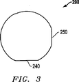
単結晶スピネルウェハにおける{22−4}面群の面と{001}へき開面群との関係は、図2に示される。<111>配向基板ウェハ200は、前面210、裏面220および面210、220の間に外周端230を有する。1つの態様において、大きいほうの平面240は{22−4}面群の面に沿って外周端230に研削される。大きいほうの平面240はウェハ200がブールからスライシングされる前に、ブールに研削されるのが通常であるが、所望ならばスライシング後に研削されうる。
The relationship between the {22-4} plane group and the {001} cleaved plane group in the single crystal spinel wafer is shown in FIG. <111>
図2に示されるように、へき開面260と前面210の交点により形成される点の軌跡は平面240に平行な線を形成する。その態様に示されるように、前面および主たる平面に沿って張り出された線は互いに平行であり、異なる配向が使用され得、たとえば大きいほうの平面と張り出された線の間の、零度でない所定角度である。{001}へき開面260に沿ってウェハ200において開始されるへき開は、ウェハ200の前面210と、大きいほうの平面240に平行に交差する。これは特に有利である。なぜなら、<111>スピネルウェハ200上に成長した(0001)AlxGa1-x-yInyNのエピタキシャル層の(10−10)へき開面はウェハ200において{001}へき開面260と並んでいるからである。すなわち、AlxGa1-x-yInyNエピタキシャル層の(10−10)へき開面の端部はウェハへき開面−前面交点で形成される点の軌跡に実質的に平行である。
As shown in FIG. 2, the locus of the point formed by the intersection of the
図2および3に示されるように、第2の、小さいほうの平面250は外周端230に研削され、第1の平面の面に平行でない面、たとえば{02−2}および {01−1}面群における面、に沿って延びるのが通常であり、そしてさらに大きいほうの面に平行でない{22−4}および {11−2}面群の面を含む。第2平面は、へき開面のへき開伝播の方向を示す。好適には、小さいほうの平面250はウェハ200がブールからスライシングされる前に、ブールに研削される。しかし、所望ならば小さいほうの平面250は、スライシング後にウェハ200に研削されうる。
As shown in FIGS. 2 and 3, the second,
図2に示されるように、ウェハはへき開面が大きいほうの平面から勾配をつけられるように配向される。もっと正確には、各へき開面は線を形成する点の軌跡に沿って裏面と交差し、裏面に沿う線は前面と大きいほうの平面に沿う線間の間隔よりも大きい距離で大きいほうの平面から間隔を置いている。この配向、前面から大きいほうの平面に対する下方への勾配、はここでは「負」の勾配と考えられる。各面は、図2に示されるように、約40〜60度、測定すると通常約55度、の範囲で、前面と角度をなす。
スピネル構造において、大きいほうの平面への法線(垂直線)および第2平面への法線は同一面にあるので、これらの法線は互いに交差し、たとえば互いに60,90、120もしくは150度の角度をなす。たとえば、(02−2)/(01−1)面に沿って延びる小さいほうの平面への法線は、{22−4}/{11−2}面群の面に沿って延びる大きいほうの平面への法線に30,90および150度の角度をなす。(22−4)/(11−2)面に沿って延びる小さいほうの平面への法線は、たとえば{11−2}/{22−4}面群の面に沿って延びる大きいほうの平面への法線に60度の角度をなしうる。ここに述べるように配向された、大きいほうおよび小さいほうの平面を用いることにより、ウェハ200は正確に配向されうる。
As shown in FIG. 2, the wafer is oriented so that the cleavage plane is sloped from the larger plane. More precisely, each cleavage plane intersects the back side along the locus of points forming the line, and the line along the back side is the larger plane at a distance greater than the spacing between the lines along the front side and the larger plane. Is spaced from. This orientation, the downward gradient from the front surface to the larger plane, is considered herein as a “negative” gradient. As shown in FIG. 2, each surface forms an angle with the front surface in a range of about 40 to 60 degrees, usually about 55 degrees when measured.
In the spinel structure, the normal to the larger plane (vertical line) and the normal to the second plane are in the same plane, so these normals intersect each other, for example 60, 90, 120 or 150 degrees to each other. Make an angle. For example, the normal to the smaller plane extending along the (02-2) / (01-1) plane is the larger one extending along the plane of the {22-4} / {11-2} plane group. Make an angle of 30, 90 and 150 degrees to the normal to the plane. The normal to the smaller plane extending along the (22-4) / (11-2) plane is, for example, the larger plane extending along the plane of the {11-2} / {22-4} plane group. An angle of 60 degrees can be made to the normal to. By using the larger and smaller planes oriented as described herein, the
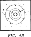
ブール110の配向は、ラウエカメラでの後方散乱電子画像化のような電子画像化の助けにより、完成される。この方法は図4A〜Dおよび5A〜Cの助力で説明されうる。図4A〜Dは単結晶スピネルの種々の配向の後方散乱写真である。図4Aおよび5Bは、形成された<111>配向されたスピネル単結晶を示し、三角形の断面130が頂点を有するとき、大きいほうの平面240は頂点に対向して三角形の底面であり、そしてカメラに対向する面は前面210である。
The orientation of the
画像化を実行する際に、第1にネック部分およびテール部分は成長したままのブール100から除去され、配向した円筒状ブールの対向端に第1および第2平面表面を残すので、ブールの中心軸は平面端部表面に垂直であり、<111>方向に通常平行である。通常平行であることにより、その軸は一般的に<111>方向の5度以内、通常3度以内、そして望ましくは2度以内である。ある態様によれば1度以内である(0度が厳密な平行を示す)。ついで、ブール110は後方散乱法で画像化される。図4Bはカメラに対向する面として裏面を示す。前面210および裏面220が確認されると、大きい方の平面240および小さいほうの平面250がブール110に研削される。1つの態様によれば、ブール110から切り出され、前面を上に向けて配向したウェハ200は、小さいほうの平面250が大きい方の平面240から間隔をおいているので、法線は反時計回りに約180度より小さい角度をなす。この配置によれば、ウェハは加工処理操作時に適切に配向され得、たとえばエピ層堆積のための基板表面上に通常実施される仕上げ操作に適切な配向である。さらに、電子もしくは光電子デバイスの製造者は成長エピ層用表面を適切に確認し、エピタキシャル成長のためにウェハを配向しうる。
In performing the imaging, first the neck and tail portions are removed from the as-grown boule 100, leaving the first and second planar surfaces at opposite ends of the oriented cylindrical boule, so that the center of the boule The axis is perpendicular to the planar end surface and is usually parallel to the <111> direction. By being normally parallel, its axis is generally within 5 degrees of the <111> direction, usually within 3 degrees, and preferably within 2 degrees. In one embodiment, it is within 1 degree (0 degree indicates strict parallelism). The
1つの態様によれば、光電子デバイスは本発明の開示に基づいてウェハを用いて作製される。その方法によれば、AlxGa1-x-yInyNエピ層は、ウェハ上に成長させるのが通常である。Xおよびyの値はともに0から1まで変動しうる。好適には、0≦x≦0.25および0≦y≦0.5である。AlxGa1-x-yInyNエピ層のへき開面の端部はウェハの前面における(001)へき開面の張り出しに通常平行である。変動する濃度の付加的層を、作製されるべきデバイスに依存して、必要に応じて成長させうる。さらに、パターニングおよびコンタクト層形成のような、いくつかの付加的工程もLEDおよびレーザーダイオードを作製するために実施されうる。実際のデバイス作製の詳細は当業者に知られており、この開示の範囲を超える。 According to one aspect, an optoelectronic device is fabricated using a wafer in accordance with the present disclosure. According to that method, the Al x Ga 1-xy In y N epilayer is usually grown on a wafer. Both the values of X and y can vary from 0 to 1. Preferably, 0 ≦ x ≦ 0.25 and 0 ≦ y ≦ 0.5. The edge of the cleavage plane of the Al x Ga 1-xy In y N epilayer is usually parallel to the overhang of the (001) cleavage plane on the front surface of the wafer. Additional layers of varying concentrations can be grown as needed, depending on the device to be fabricated. In addition, some additional steps, such as patterning and contact layer formation, can also be performed to make LEDs and laser diodes. Details of actual device fabrication are known to those skilled in the art and are beyond the scope of this disclosure.
例
チョクラルスキー法により成長したブール(インゴット)は2つの平らな表面を製造するために頂部とテール部分を除去された。ブール端部(2つの平らな表面)はラウエ後方散乱法を用いてX線解析により、配向を確認し、さらに次の点を確認した。1)(100)へき開面が、得られるウェハの底面から頂面にへき開するであろうこと(ここで底面の交線は頂面の交線よりも、形成されるべき大きい方の平面から離れている)を確実にするために、得られるであろうウェハのための前面、ならびに2)大きい方の平面(11−2)(もしくは(22−4))および小さいほうの平面(01−1)(もしくは(02−2))のほぼ正確な位置。ついで、ブール端部はX線解析により、配向を測定され、ブールの軸を<111>方向に調整された。
Example A boule (ingot) grown by the Czochralski method was stripped of the top and tail portions to produce two flat surfaces. The orientation of the boule ends (two flat surfaces) was confirmed by X-ray analysis using the Laue backscattering method, and the following points were further confirmed. 1) The (100) cleavage plane will be cleaved from the bottom surface of the resulting wafer to the top surface (where the intersection line of the bottom surface is far from the larger plane to be formed than the intersection line of the top surface) 2) the front surface for the wafer that will be obtained , and 2) the larger plane (11-2) (or (22-4)) and the smaller plane (01-1) ) (Or (02-2)). The boule end was then measured for orientation by X-ray analysis and the boule axis was adjusted in the <111> direction.
ついで、111方向(すなわち中心軸は<111>配向に平行であった)にまさに平行である円筒体を形成するために、ブールは回転され約2インチ(約5.1cm)の径にされた。この時点で、大きい方の平面および小さいほうの平面方向がスクライビングにより
頂面上にマークされた。ついで、大きい方の平面および小さいほうの平面は、<111>方向に垂直である方向に沿って材料を除去するためにブール外周を研削することにより、円筒体に付加され、それにより形成された平面は<111>方向に平行に延びた。ついで、回転ブールは個別のウェハブランクにスライシングされた。個別のウェハブランクはラッピングされ、研削により傾斜角を付与され、連続番号がレーザーを用いて記入され、そしてエピタキシャル層成長に適した表面を与えるために前面に沿ってポリッシングされた。
The boule was then rotated to a diameter of about 2 inches (about 5.1 cm) to form a cylinder that was just parallel to the 111 direction (ie, the central axis was parallel to the <111> orientation). . At this point, the larger plane and the smaller plane direction were marked on the top surface by scribing. The larger and smaller planes were then added to and formed by the cylinder by grinding the boule periphery to remove material along a direction that is perpendicular to the <111> direction. The plane extended parallel to the <111> direction. The rotating boule was then sliced into individual wafer blanks. Individual wafer blanks were lapped, tilted by grinding, serial numbers entered using a laser, and polished along the front surface to provide a surface suitable for epitaxial layer growth.
上記の説明は例証および説明のために示されたものである。徹底的なものでもなく、また開示された正確な形態もしくは態様にその範囲に限定することは意図されておらず、変更および変形も上記の教示から可能であり、または本発明の態様の実施から得られうる。 The above description has been presented for purposes of illustration and description. It is not exhaustive and is not intended to be limited in scope to the precise forms or embodiments disclosed, variations and modifications are possible from the above teachings, or from practice of embodiments of the invention Can be obtained.
Claims (16)
該ウェハが<111>結晶学的配向を有しており、第1平面は{22−4}および{11−2}面群の1つにおける面に沿って延び、また第2平面は{02−2}、{01−1}、{22−4}および{11−2}面群の1つの面に沿って延び、そして第2平面は第1平面の面に平行でないウェハの製造方法。Forming a single crystal boule having a <111>orientation; forming first and second planes in the boule; slicing the boule to a wafer; and first and second at the first and second ends of the boule Forming two opposing planar surfaces, wherein the first and second planes identify the front and back surfaces of the wafer, which identifies the orientation of the cleavage plane of the wafer, the planar surfaces comprising the first and first A method of manufacturing a wafer, wherein the boule central axis extending perpendicular to the two planar surfaces is adjusted to be adjusted within 5 degrees of the <111> direction,
The wafer has a <111> crystallographic orientation, the first plane extends along a plane in one of the {22-4} and {11-2} plane groups, and the second plane is {02 -2}, {01-1}, {22-4} and {11-2} A method of manufacturing a wafer extending along one surface of the plane group, and the second plane is not parallel to the plane of the first plane.
Applications Claiming Priority (3)
| Application Number | Priority Date | Filing Date | Title |
|---|---|---|---|
| US10/668,610 | 2003-09-23 | ||
| US10/668,610 US7326477B2 (en) | 2003-09-23 | 2003-09-23 | Spinel boules, wafers, and methods for fabricating same |
| PCT/US2004/030800 WO2005031046A1 (en) | 2003-09-23 | 2004-09-17 | Spinel boules, wafers, and methods for fabricating same |
Publications (3)
| Publication Number | Publication Date |
|---|---|
| JP2007506639A JP2007506639A (en) | 2007-03-22 |
| JP2007506639A5 JP2007506639A5 (en) | 2010-05-20 |
| JP4949839B2 true JP4949839B2 (en) | 2012-06-13 |
Family
ID=34313522
Family Applications (1)
| Application Number | Title | Priority Date | Filing Date |
|---|---|---|---|
| JP2006528092A Expired - Fee Related JP4949839B2 (en) | 2003-09-23 | 2004-09-17 | Spinel boules, wafers and methods for their production |
Country Status (9)
| Country | Link |
|---|---|
| US (1) | US7326477B2 (en) |
| EP (1) | EP1670975B1 (en) |
| JP (1) | JP4949839B2 (en) |
| AT (1) | ATE510940T1 (en) |
| IL (1) | IL174351A0 (en) |
| MY (1) | MY137813A (en) |
| RU (1) | RU2335582C2 (en) |
| TW (1) | TWI290965B (en) |
| WO (1) | WO2005031046A1 (en) |
Families Citing this family (7)
| Publication number | Priority date | Publication date | Assignee | Title |
|---|---|---|---|---|
| US8161388B2 (en) * | 2004-01-21 | 2012-04-17 | Rodriguez Arturo A | Interactive discovery of display device characteristics |
| US7919815B1 (en) * | 2005-02-24 | 2011-04-05 | Saint-Gobain Ceramics & Plastics, Inc. | Spinel wafers and methods of preparation |
| EP2168935A1 (en) | 2008-09-29 | 2010-03-31 | Siemens Aktiengesellschaft | Material compound for producing a fire-retardant material and its application and fire-retardant moulding body and method for its manufacture |
| DE102009013685B4 (en) | 2009-03-20 | 2013-01-31 | Novaled Ag | Use of an organic diode as organic Zener diode and method of operation |
| DE102012003483B3 (en) | 2012-02-21 | 2013-02-21 | Technische Universität Bergakademie Freiberg | Thermal shock and corrosion resistant ceramic based on calcium zirconate and process for its preparation |
| JP6623759B2 (en) * | 2014-09-08 | 2019-12-25 | 住友電気工業株式会社 | Silicon carbide single crystal substrate and method of manufacturing the same |
| JP7128067B2 (en) * | 2018-09-14 | 2022-08-30 | 株式会社ディスコ | WAFER PRODUCTION METHOD AND LASER PROCESSING APPARATUS |
Family Cites Families (101)
| Publication number | Priority date | Publication date | Assignee | Title |
|---|---|---|---|---|
| US2634554A (en) * | 1953-04-14 | Synthetic gem production | ||
| DE1544261C3 (en) * | 1965-03-30 | 1975-12-18 | Siemens Ag, 1000 Berlin Und 8000 Muenchen | Process for the epitaxial deposition of a monocrystalline layer of a semiconductor material crystallizing according to the diamond or zincblende grid |
| FR1471976A (en) | 1965-03-30 | 1967-03-03 | Siemens Ag | Process for epitaxially depositing a semiconductor substance crystallizing in the diamond lattice or in that of the blende |
| US3885978A (en) * | 1968-05-31 | 1975-05-27 | Matsushita Electric Works Ltd | Inorganic coating composition |
| FR1597033A (en) * | 1968-06-19 | 1970-06-22 | ||
| DE1769635A1 (en) * | 1968-06-20 | 1972-03-30 | Siemens Ag | Thin semiconductor growth layer on low-alumina, crucible-drawn magnesium-aluminum spinel single crystal, as well as processes for the production of the layer and for the production of the single crystals |
| US3658586A (en) * | 1969-04-11 | 1972-04-25 | Rca Corp | Epitaxial silicon on hydrogen magnesium aluminate spinel single crystals |
| US3816906A (en) * | 1969-06-20 | 1974-06-18 | Siemens Ag | Method of dividing mg-al spinel substrate wafers coated with semiconductor material and provided with semiconductor components |
| US3964942A (en) * | 1970-10-16 | 1976-06-22 | International Business Machines Corporation | Chemical polishing of single crystal dielectrics |
| US3796597A (en) * | 1970-11-02 | 1974-03-12 | Texas Instruments Inc | Method of producing semiconducting monocrystalline silicon on spinel substrates |
| US3753775A (en) * | 1971-03-01 | 1973-08-21 | Rca Corp | Chemical polishing of sapphire |
| US3736158A (en) * | 1971-03-19 | 1973-05-29 | G Cullen | Czochralski-grown spinel for use as epitaxial silicon substrate |
| US3808065A (en) * | 1972-02-28 | 1974-04-30 | Rca Corp | Method of polishing sapphire and spinel |
| US4177321A (en) * | 1972-07-25 | 1979-12-04 | Semiconductor Research Foundation | Single crystal of semiconductive material on crystal of insulating material |
| US3808836A (en) * | 1972-11-30 | 1974-05-07 | H Jones | Doublet gem construction |
| US3883313A (en) * | 1972-12-14 | 1975-05-13 | Rca Corp | Modified czochralski-grown magnesium aluminate spinel and method of making same |
| US3898051A (en) * | 1973-12-28 | 1975-08-05 | Crystal Syst | Crystal growing |
| GB1488940A (en) * | 1974-03-28 | 1977-10-19 | Siemens Ag | Production of monocrystals by the verneuil method |
| JPS5117663A (en) * | 1974-08-02 | 1976-02-12 | Handotai Kenkyu Shinkokai | Handotaikibanyo supineruketsusho |
| US3950504A (en) * | 1974-09-26 | 1976-04-13 | Quigley Company, Inc. | Process for producing magnesium aluminate spinel |
| JPS5343481A (en) | 1976-10-01 | 1978-04-19 | Matsushita Electric Ind Co Ltd | Mirror surface etching method of sapphire substrate crystal |
| JPS5426873A (en) | 1977-07-30 | 1979-02-28 | Matsushita Electric Works Ltd | Method of strengthing base material of paper for resin impregnation |
| US4347210A (en) * | 1980-05-09 | 1982-08-31 | Raytheon Company | Method of forging spinel domes |
| US4370739A (en) * | 1980-06-09 | 1983-01-25 | Rca Corporation | Spinel video disc playback stylus |
| JPS5890736A (en) | 1981-11-25 | 1983-05-30 | Toshiba Corp | Sapphire substrate for semiconductor device |
| FR2521123A1 (en) * | 1982-02-09 | 1983-08-12 | Thomson Csf | PROCESS FOR PRODUCING DOPED SILICA GLASS FOR OPTICAL FIBER PREFORM PREPARATION |
| JPS58211736A (en) | 1982-06-03 | 1983-12-09 | Toshiba Corp | Manufacture of lithium niobate single crystal element |
| FR2555157B1 (en) * | 1983-11-22 | 1989-03-03 | France Etat | NOVEL MIXED OXIDES FOR PARTICULAR USE IN TUNABLE LASERS |
| JPS61134111A (en) * | 1984-12-04 | 1986-06-21 | Shin Etsu Chem Co Ltd | Lithium tantalate single crystal wafer |
| JPS61142759A (en) | 1984-12-14 | 1986-06-30 | Ngk Spark Plug Co Ltd | Substrate for ic package |
| US4657754A (en) * | 1985-11-21 | 1987-04-14 | Norton Company | Aluminum oxide powders and process |
| JPS62123059A (en) | 1985-11-25 | 1987-06-04 | 株式会社住友金属セラミックス | Ceramic composition with surface smoothness |
| JPS62188325A (en) | 1986-02-14 | 1987-08-17 | Sumitomo Electric Ind Ltd | Method and apparatus for forming orientation flat surface of compound semiconductor |
| US4790982A (en) * | 1986-04-07 | 1988-12-13 | Katalistiks International, Inc. | Metal-containing spinel composition and process of using same |
| US4819167A (en) * | 1987-04-20 | 1989-04-04 | Applied Materials, Inc. | System and method for detecting the center of an integrated circuit wafer |
| US5138298A (en) * | 1989-11-02 | 1992-08-11 | Sanken Electric Co., Ltd. | Metallic oxide resistive bodies having a nonlinear volt-ampere characteristic and method of fabrication |
| AU650382B2 (en) * | 1992-02-05 | 1994-06-16 | Norton Company | Nano-sized alpha alumina particles |
| US6258137B1 (en) * | 1992-02-05 | 2001-07-10 | Saint-Gobain Industrial Ceramics, Inc. | CMP products |
| JPH07235692A (en) | 1993-12-30 | 1995-09-05 | Sony Corp | Compound semiconductor device and forming method thereof |
| US5679152A (en) * | 1994-01-27 | 1997-10-21 | Advanced Technology Materials, Inc. | Method of making a single crystals Ga*N article |
| JPH07307316A (en) | 1994-05-12 | 1995-11-21 | Sumitomo Electric Ind Ltd | Iii-v compound semiconductor wafer and its machining method |
| US5426083A (en) | 1994-06-01 | 1995-06-20 | Amoco Corporation | Absorbent and process for removing sulfur oxides from a gaseous mixture |
| US5741729A (en) * | 1994-07-11 | 1998-04-21 | Sun Microsystems, Inc. | Ball grid array package for an integrated circuit |
| JP3559315B2 (en) | 1994-07-29 | 2004-09-02 | 京セラ株式会社 | Film composition analysis method |
| JP3015261B2 (en) | 1994-09-12 | 2000-03-06 | 科学技術振興事業団 | Heat treatment method of sapphire single crystal substrate to improve surface characteristics |
| JP3329594B2 (en) | 1994-09-28 | 2002-09-30 | 有限会社遠野精器 | Method of manufacturing sapphire substrate for photomask |
| US5643044A (en) * | 1994-11-01 | 1997-07-01 | Lund; Douglas E. | Automatic chemical and mechanical polishing system for semiconductor wafers |
| US5557624A (en) * | 1995-01-20 | 1996-09-17 | Hughes Aircraft Company | Laser system using U-doped crystal Q-switch |
| US5530267A (en) * | 1995-03-14 | 1996-06-25 | At&T Corp. | Article comprising heteroepitaxial III-V nitride semiconductor material on a substrate |
| JPH08316571A (en) * | 1995-03-16 | 1996-11-29 | Fujitsu Ltd | Semiconductor laser and manufacture thereof |
| US5850410A (en) * | 1995-03-16 | 1998-12-15 | Fujitsu Limited | Semiconductor laser and method for fabricating the same |
| US5654973A (en) * | 1995-05-05 | 1997-08-05 | Hughes Electronics | Laser system using Co2+ -doped crystal Q-switch |
| US5742026A (en) * | 1995-06-26 | 1998-04-21 | Corning Incorporated | Processes for polishing glass and glass-ceramic surfaces using excimer laser radiation |
| US5825913A (en) * | 1995-07-18 | 1998-10-20 | Cognex Corporation | System for finding the orientation of a wafer |
| JPH09129651A (en) | 1995-08-31 | 1997-05-16 | Hewlett Packard Co <Hp> | Thermal annealing method and device of sapphire substrate |
| JP2987111B2 (en) | 1995-08-31 | 1999-12-06 | 株式会社東芝 | Semiconductor device and manufacturing method thereof |
| US5802083A (en) * | 1995-12-11 | 1998-09-01 | Milton Birnbaum | Saturable absorber Q-switches for 2-μm lasers |
| US5968267A (en) * | 1996-01-25 | 1999-10-19 | General Signal Technology Corporation | Antivibration support for Czochralski crystal growing systems |
| US5644400A (en) * | 1996-03-29 | 1997-07-01 | Lam Research Corporation | Method and apparatus for determining the center and orientation of a wafer-like object |
| US5822213A (en) * | 1996-03-29 | 1998-10-13 | Lam Research Corporation | Method and apparatus for determining the center and orientation of a wafer-like object |
| JP2882355B2 (en) | 1996-04-10 | 1999-04-12 | 住友電気工業株式会社 | III-V compound semiconductor wafer and method of manufacturing the same |
| US6021380A (en) * | 1996-07-09 | 2000-02-01 | Scanis, Inc. | Automatic semiconductor wafer sorter/prober with extended optical inspection |
| US6533874B1 (en) * | 1996-12-03 | 2003-03-18 | Advanced Technology Materials, Inc. | GaN-based devices using thick (Ga, Al, In)N base layers |
| US5741724A (en) | 1996-12-27 | 1998-04-21 | Motorola | Method of growing gallium nitride on a spinel substrate |
| FR2758915B1 (en) * | 1997-01-30 | 1999-03-05 | Commissariat Energie Atomique | SOLID MICROLASER PASSIVELY TRIGGERED BY SATURABLE ABSORBENT AND MANUFACTURING METHOD THEREOF |
| USRE38489E1 (en) | 1997-01-30 | 2004-04-06 | Commissariat A L'energie Atomique | Solid microlaser passively switched by a saturable absorber and its production process |
| US5768335A (en) * | 1997-02-10 | 1998-06-16 | Lucent Technologies Inc. | Apparatus and method for measuring the orientation of a single crystal surface |
| JP3652861B2 (en) | 1997-11-27 | 2005-05-25 | 京セラ株式会社 | Thin film growth substrate and light emitting device using the same |
| US5982796A (en) * | 1997-12-16 | 1999-11-09 | Union Carbide Chemicals & Plastics | 2.7 μM laser crystalline material utilizing multiple-channel optical pumping |
| JP3805883B2 (en) | 1997-12-26 | 2006-08-09 | 東芝電子エンジニアリング株式会社 | Gallium nitride based semiconductor wafer, gallium nitride based semiconductor device, and manufacturing method thereof |
| JPH11235659A (en) | 1998-02-18 | 1999-08-31 | Ricoh Co Ltd | Chemically removing processing method induced by friction and working device thereof |
| US5989301A (en) * | 1998-02-18 | 1999-11-23 | Saint-Gobain Industrial Ceramics, Inc. | Optical polishing formulation |
| JP3338360B2 (en) | 1998-03-23 | 2002-10-28 | 三洋電機株式会社 | Gallium nitride based semiconductor wafer manufacturing method |
| DE69827768D1 (en) * | 1998-04-02 | 2004-12-30 | Comadur Sa | Watch glass with a lens and method for producing such a lens |
| DE69915428T2 (en) | 1998-10-27 | 2005-02-17 | Corning Inc. | Glass ceramics with low expansion |
| JP4097343B2 (en) * | 1999-01-26 | 2008-06-11 | 日亜化学工業株式会社 | Manufacturing method of nitride semiconductor laser device |
| KR100304664B1 (en) | 1999-02-05 | 2001-09-26 | 윤종용 | Method for fabricating a GaN film |
| US6104529A (en) * | 1999-03-08 | 2000-08-15 | Lucent Technologies Inc. | Optical fiber communication system employing wide band crystal alloy light generation devices |
| US6238450B1 (en) * | 1999-06-16 | 2001-05-29 | Saint-Gobain Industrial Ceramics, Inc. | Ceria powder |
| US6265089B1 (en) * | 1999-07-15 | 2001-07-24 | The United States Of America As Represented By The Secretary Of The Navy | Electronic devices grown on off-axis sapphire substrate |
| CN1154194C (en) | 1999-08-30 | 2004-06-16 | 光磊科技股份有限公司 | Base plate structure of LED |
| US6366596B1 (en) * | 2000-01-21 | 2002-04-02 | Photonics Industries International, Inc. | High power laser |
| JP3662806B2 (en) * | 2000-03-29 | 2005-06-22 | 日本電気株式会社 | Method for manufacturing nitride-based semiconductor layer |
| US6364920B1 (en) * | 2000-04-21 | 2002-04-02 | Saint-Gobain Ceramics & Plastics, Inc. | CMP formulations |
| US6391072B1 (en) * | 2000-05-04 | 2002-05-21 | Saint-Gobain Industrial Ceramics, Inc. | Abrasive grain |
| US6746777B1 (en) * | 2000-05-31 | 2004-06-08 | Applied Optoelectronics, Inc. | Alternative substrates for epitaxial growth |
| US6627974B2 (en) * | 2000-06-19 | 2003-09-30 | Nichia Corporation | Nitride semiconductor substrate and method for manufacturing the same, and nitride semiconductor device using nitride semiconductor substrate |
| US7064355B2 (en) * | 2000-09-12 | 2006-06-20 | Lumileds Lighting U.S., Llc | Light emitting diodes with improved light extraction efficiency |
| US6657237B2 (en) * | 2000-12-18 | 2003-12-02 | Samsung Electro-Mechanics Co., Ltd. | GaN based group III-V nitride semiconductor light-emitting diode and method for fabricating the same |
| US6418921B1 (en) * | 2001-01-24 | 2002-07-16 | Crystal Systems, Inc. | Method and apparatus for cutting workpieces |
| US6839362B2 (en) * | 2001-05-22 | 2005-01-04 | Saint-Gobain Ceramics & Plastics, Inc. | Cobalt-doped saturable absorber Q-switches and laser systems |
| JP3768943B2 (en) | 2001-09-28 | 2006-04-19 | 日本碍子株式会社 | Group III nitride epitaxial substrate, group III nitride device epitaxial substrate, and group III nitride device |
| AU2002360466A1 (en) * | 2001-12-04 | 2003-06-17 | Landauer, Inc. | Aluminum oxide material for optical data storage |
| US6844084B2 (en) * | 2002-04-03 | 2005-01-18 | Saint-Gobain Ceramics & Plastics, Inc. | Spinel substrate and heteroepitaxial growth of III-V materials thereon |
| US6818532B2 (en) * | 2002-04-09 | 2004-11-16 | Oriol, Inc. | Method of etching substrates |
| CN1167140C (en) | 2002-05-17 | 2004-09-15 | 清华大学 | Process for treating substrate of epitaxial chip for high-brightness gallium nitride-base LED |
| KR100499129B1 (en) | 2002-09-02 | 2005-07-04 | 삼성전기주식회사 | Light emitting laser diode and fabricatin method thereof |
| CN1227730C (en) | 2003-04-30 | 2005-11-16 | 东莞市福地电子材料有限公司 | Processing method of nano level saphire substrate and its special polishing liquid |
| CN1204598C (en) | 2003-06-27 | 2005-06-01 | 中国科学院上海光学精密机械研究所 | Preparation method of γ-LiAlO2/α-Al2O3 composite substrate material |
| CN1207756C (en) | 2003-06-27 | 2005-06-22 | 中国科学院上海光学精密机械研究所 | ZnAl2O4/α-Al2O3Preparation method of composite substrate material |
| US7045223B2 (en) * | 2003-09-23 | 2006-05-16 | Saint-Gobain Ceramics & Plastics, Inc. | Spinel articles and methods for forming same |
-
2003
- 2003-09-23 US US10/668,610 patent/US7326477B2/en not_active Expired - Fee Related
-
2004
- 2004-09-17 JP JP2006528092A patent/JP4949839B2/en not_active Expired - Fee Related
- 2004-09-17 EP EP04788857A patent/EP1670975B1/en not_active Expired - Lifetime
- 2004-09-17 WO PCT/US2004/030800 patent/WO2005031046A1/en active Application Filing
- 2004-09-17 RU RU2006109199/15A patent/RU2335582C2/en not_active IP Right Cessation
- 2004-09-17 AT AT04788857T patent/ATE510940T1/en not_active IP Right Cessation
- 2004-09-21 MY MYPI20043855A patent/MY137813A/en unknown
- 2004-09-23 TW TW093128800A patent/TWI290965B/en not_active IP Right Cessation
-
2006
- 2006-03-16 IL IL174351A patent/IL174351A0/en unknown
Also Published As
| Publication number | Publication date |
|---|---|
| TW200513550A (en) | 2005-04-16 |
| TWI290965B (en) | 2007-12-11 |
| US7326477B2 (en) | 2008-02-05 |
| JP2007506639A (en) | 2007-03-22 |
| ATE510940T1 (en) | 2011-06-15 |
| WO2005031046A1 (en) | 2005-04-07 |
| IL174351A0 (en) | 2006-08-01 |
| MY137813A (en) | 2009-03-31 |
| EP1670975B1 (en) | 2011-05-25 |
| EP1670975A1 (en) | 2006-06-21 |
| RU2006109199A (en) | 2006-09-10 |
| RU2335582C2 (en) | 2008-10-10 |
| US20050061231A1 (en) | 2005-03-24 |
Similar Documents
| Publication | Publication Date | Title |
|---|---|---|
| JP5562905B2 (en) | Spinel article and manufacturing method thereof | |
| US10100434B2 (en) | Nitride semiconductor single crystal substrate manufacturing method | |
| KR100655106B1 (en) | Spinel substrate and heteroepitaxial growth of III-V materials thereon | |
| CN113423876B (en) | Gallium arsenide single crystal substrate | |
| JP4949839B2 (en) | Spinel boules, wafers and methods for their production | |
| US11377757B2 (en) | Method for producing group III nitride crystal and seed substrate | |
| KR101522777B1 (en) | Group 13 nitride crystal, group 13 nitride crystal substrate, and method of manufacturing group 13 nitride crystal | |
| RU2334835C2 (en) | Method of fabrication of mono crystal spinel plates (versions) | |
| EP1670976B1 (en) | Spinel articles | |
| JP2016074553A (en) | Method for manufacturing group iii nitride semiconductor single crystal substrate | |
| US20230352298A1 (en) | Group-iii element nitride semiconductor substrate | |
| WO2016040533A1 (en) | Substrates for growing group iii nitride crystals and their fabrication method | |
| JP5883912B2 (en) | Nitride crystal and method for producing the same | |
| JP2000247790A (en) | Substrate for semiconductor element, semiconductor element and production of nitrogen compound single crystal substrate | |
| JPH09309793A (en) | Production of epitaxial wafer and single crystal substrate using the same | |
| JP2016172692A (en) | Nitride crystal and production method thereof | |
| JP2002167296A (en) | Substrate for film forming | |
| JP2015078121A (en) | Nitride crystal and its production method |
Legal Events
| Date | Code | Title | Description |
|---|---|---|---|
| A131 | Notification of reasons for refusal |
Free format text: JAPANESE INTERMEDIATE CODE: A131 Effective date: 20091110 |
|
| A601 | Written request for extension of time |
Free format text: JAPANESE INTERMEDIATE CODE: A601 Effective date: 20100209 |
|
| A602 | Written permission of extension of time |
Free format text: JAPANESE INTERMEDIATE CODE: A602 Effective date: 20100217 |
|
| A524 | Written submission of copy of amendment under article 19 pct |
Free format text: JAPANESE INTERMEDIATE CODE: A524 Effective date: 20100331 |
|
| A131 | Notification of reasons for refusal |
Free format text: JAPANESE INTERMEDIATE CODE: A131 Effective date: 20101012 |
|
| A601 | Written request for extension of time |
Free format text: JAPANESE INTERMEDIATE CODE: A601 Effective date: 20110111 |
|
| A602 | Written permission of extension of time |
Free format text: JAPANESE INTERMEDIATE CODE: A602 Effective date: 20110118 |
|
| A521 | Request for written amendment filed |
Free format text: JAPANESE INTERMEDIATE CODE: A523 Effective date: 20110411 |
|
| A521 | Request for written amendment filed |
Free format text: JAPANESE INTERMEDIATE CODE: A523 Effective date: 20110412 |
|
| TRDD | Decision of grant or rejection written | ||
| A01 | Written decision to grant a patent or to grant a registration (utility model) |
Free format text: JAPANESE INTERMEDIATE CODE: A01 Effective date: 20120207 |
|
| A01 | Written decision to grant a patent or to grant a registration (utility model) |
Free format text: JAPANESE INTERMEDIATE CODE: A01 |
|
| A61 | First payment of annual fees (during grant procedure) |
Free format text: JAPANESE INTERMEDIATE CODE: A61 Effective date: 20120308 |
|
| FPAY | Renewal fee payment (event date is renewal date of database) |
Free format text: PAYMENT UNTIL: 20150316 Year of fee payment: 3 |
|
| R150 | Certificate of patent or registration of utility model |
Free format text: JAPANESE INTERMEDIATE CODE: R150 |
|
| R250 | Receipt of annual fees |
Free format text: JAPANESE INTERMEDIATE CODE: R250 |
|
| R250 | Receipt of annual fees |
Free format text: JAPANESE INTERMEDIATE CODE: R250 |
|
| R250 | Receipt of annual fees |
Free format text: JAPANESE INTERMEDIATE CODE: R250 |
|
| LAPS | Cancellation because of no payment of annual fees |