JP4939737B2 - Light emitting device - Google Patents
Light emitting device Download PDFInfo
- Publication number
- JP4939737B2 JP4939737B2 JP2004225146A JP2004225146A JP4939737B2 JP 4939737 B2 JP4939737 B2 JP 4939737B2 JP 2004225146 A JP2004225146 A JP 2004225146A JP 2004225146 A JP2004225146 A JP 2004225146A JP 4939737 B2 JP4939737 B2 JP 4939737B2
- Authority
- JP
- Japan
- Prior art keywords
- tft
- potential
- light emitting
- emitting element
- gate
- Prior art date
- Legal status (The legal status is an assumption and is not a legal conclusion. Google has not performed a legal analysis and makes no representation as to the accuracy of the status listed.)
- Active
Links
- 239000003990 capacitor Substances 0.000 claims description 30
- 239000011159 matrix material Substances 0.000 claims description 7
- 239000010408 film Substances 0.000 description 257
- 239000004065 semiconductor Substances 0.000 description 160
- 239000010410 layer Substances 0.000 description 73
- 239000000758 substrate Substances 0.000 description 56
- 238000000034 method Methods 0.000 description 41
- 230000015572 biosynthetic process Effects 0.000 description 24
- 239000012535 impurity Substances 0.000 description 24
- 239000007789 gas Substances 0.000 description 20
- 230000006870 function Effects 0.000 description 17
- 239000000463 material Substances 0.000 description 17
- 229910052581 Si3N4 Inorganic materials 0.000 description 15
- 229910052782 aluminium Inorganic materials 0.000 description 15
- 238000002161 passivation Methods 0.000 description 15
- HQVNEWCFYHHQES-UHFFFAOYSA-N silicon nitride Chemical compound N12[Si]34N5[Si]62N3[Si]51N64 HQVNEWCFYHHQES-UHFFFAOYSA-N 0.000 description 15
- XKRFYHLGVUSROY-UHFFFAOYSA-N Argon Chemical compound [Ar] XKRFYHLGVUSROY-UHFFFAOYSA-N 0.000 description 12
- XAGFODPZIPBFFR-UHFFFAOYSA-N aluminium Chemical compound [Al] XAGFODPZIPBFFR-UHFFFAOYSA-N 0.000 description 10
- 239000010936 titanium Substances 0.000 description 10
- QVGXLLKOCUKJST-UHFFFAOYSA-N atomic oxygen Chemical compound [O] QVGXLLKOCUKJST-UHFFFAOYSA-N 0.000 description 9
- 239000001301 oxygen Substances 0.000 description 9
- 229910052760 oxygen Inorganic materials 0.000 description 9
- 239000002356 single layer Substances 0.000 description 9
- 238000004519 manufacturing process Methods 0.000 description 8
- 229910021332 silicide Inorganic materials 0.000 description 8
- FVBUAEGBCNSCDD-UHFFFAOYSA-N silicide(4-) Chemical compound [Si-4] FVBUAEGBCNSCDD-UHFFFAOYSA-N 0.000 description 8
- 238000005530 etching Methods 0.000 description 7
- 229920005989 resin Polymers 0.000 description 7
- 239000011347 resin Substances 0.000 description 7
- 229910052719 titanium Inorganic materials 0.000 description 7
- IJGRMHOSHXDMSA-UHFFFAOYSA-N Atomic nitrogen Chemical compound N#N IJGRMHOSHXDMSA-UHFFFAOYSA-N 0.000 description 6
- RTAQQCXQSZGOHL-UHFFFAOYSA-N Titanium Chemical compound [Ti] RTAQQCXQSZGOHL-UHFFFAOYSA-N 0.000 description 6
- 229910052786 argon Inorganic materials 0.000 description 6
- 239000013078 crystal Substances 0.000 description 6
- 238000010586 diagram Methods 0.000 description 6
- 238000005192 partition Methods 0.000 description 6
- 230000001681 protective effect Effects 0.000 description 6
- 229910052710 silicon Inorganic materials 0.000 description 6
- VYPSYNLAJGMNEJ-UHFFFAOYSA-N Silicium dioxide Chemical compound O=[Si]=O VYPSYNLAJGMNEJ-UHFFFAOYSA-N 0.000 description 5
- 239000000956 alloy Substances 0.000 description 5
- 238000000354 decomposition reaction Methods 0.000 description 5
- 230000006866 deterioration Effects 0.000 description 5
- 239000000126 substance Substances 0.000 description 5
- XUIMIQQOPSSXEZ-UHFFFAOYSA-N Silicon Chemical compound [Si] XUIMIQQOPSSXEZ-UHFFFAOYSA-N 0.000 description 4
- NIXOWILDQLNWCW-UHFFFAOYSA-N acrylic acid group Chemical group C(C=C)(=O)O NIXOWILDQLNWCW-UHFFFAOYSA-N 0.000 description 4
- 229910045601 alloy Inorganic materials 0.000 description 4
- KPUWHANPEXNPJT-UHFFFAOYSA-N disiloxane Chemical class [SiH3]O[SiH3] KPUWHANPEXNPJT-UHFFFAOYSA-N 0.000 description 4
- 230000000694 effects Effects 0.000 description 4
- 230000005684 electric field Effects 0.000 description 4
- 239000001257 hydrogen Substances 0.000 description 4
- 229910052739 hydrogen Inorganic materials 0.000 description 4
- 238000002347 injection Methods 0.000 description 4
- 239000007924 injection Substances 0.000 description 4
- 229920003023 plastic Polymers 0.000 description 4
- 239000004033 plastic Substances 0.000 description 4
- 230000008569 process Effects 0.000 description 4
- 239000000565 sealant Substances 0.000 description 4
- 239000010703 silicon Substances 0.000 description 4
- 229910052814 silicon oxide Inorganic materials 0.000 description 4
- ZOXJGFHDIHLPTG-UHFFFAOYSA-N Boron Chemical compound [B] ZOXJGFHDIHLPTG-UHFFFAOYSA-N 0.000 description 3
- UFHFLCQGNIYNRP-UHFFFAOYSA-N Hydrogen Chemical compound [H][H] UFHFLCQGNIYNRP-UHFFFAOYSA-N 0.000 description 3
- 239000004642 Polyimide Substances 0.000 description 3
- NRTOMJZYCJJWKI-UHFFFAOYSA-N Titanium nitride Chemical compound [Ti]#N NRTOMJZYCJJWKI-UHFFFAOYSA-N 0.000 description 3
- XLOMVQKBTHCTTD-UHFFFAOYSA-N Zinc monoxide Chemical compound [Zn]=O XLOMVQKBTHCTTD-UHFFFAOYSA-N 0.000 description 3
- 125000004429 atom Chemical group 0.000 description 3
- 229910052796 boron Inorganic materials 0.000 description 3
- 239000010949 copper Substances 0.000 description 3
- 239000000945 filler Substances 0.000 description 3
- 239000011521 glass Substances 0.000 description 3
- 229910003437 indium oxide Inorganic materials 0.000 description 3
- PJXISJQVUVHSOJ-UHFFFAOYSA-N indium(iii) oxide Chemical compound [O-2].[O-2].[O-2].[In+3].[In+3] PJXISJQVUVHSOJ-UHFFFAOYSA-N 0.000 description 3
- 239000004973 liquid crystal related substance Substances 0.000 description 3
- 229910052757 nitrogen Inorganic materials 0.000 description 3
- 229920001721 polyimide Polymers 0.000 description 3
- 229920002620 polyvinyl fluoride Polymers 0.000 description 3
- 238000004544 sputter deposition Methods 0.000 description 3
- 229910052721 tungsten Inorganic materials 0.000 description 3
- 239000010937 tungsten Substances 0.000 description 3
- 229910017073 AlLi Inorganic materials 0.000 description 2
- 229920002799 BoPET Polymers 0.000 description 2
- RYGMFSIKBFXOCR-UHFFFAOYSA-N Copper Chemical compound [Cu] RYGMFSIKBFXOCR-UHFFFAOYSA-N 0.000 description 2
- ZOKXTWBITQBERF-UHFFFAOYSA-N Molybdenum Chemical compound [Mo] ZOKXTWBITQBERF-UHFFFAOYSA-N 0.000 description 2
- 239000005041 Mylar™ Substances 0.000 description 2
- 239000004952 Polyamide Substances 0.000 description 2
- 229910018557 Si O Inorganic materials 0.000 description 2
- ATJFFYVFTNAWJD-UHFFFAOYSA-N Tin Chemical compound [Sn] ATJFFYVFTNAWJD-UHFFFAOYSA-N 0.000 description 2
- DQXBYHZEEUGOBF-UHFFFAOYSA-N but-3-enoic acid;ethene Chemical compound C=C.OC(=O)CC=C DQXBYHZEEUGOBF-UHFFFAOYSA-N 0.000 description 2
- 229910052802 copper Inorganic materials 0.000 description 2
- 238000002425 crystallisation Methods 0.000 description 2
- 230000008025 crystallization Effects 0.000 description 2
- 238000007865 diluting Methods 0.000 description 2
- 239000005038 ethylene vinyl acetate Substances 0.000 description 2
- 230000005281 excited state Effects 0.000 description 2
- 239000011152 fibreglass Substances 0.000 description 2
- 230000005283 ground state Effects 0.000 description 2
- 238000010438 heat treatment Methods 0.000 description 2
- 239000001307 helium Substances 0.000 description 2
- 229910052734 helium Inorganic materials 0.000 description 2
- SWQJXJOGLNCZEY-UHFFFAOYSA-N helium atom Chemical compound [He] SWQJXJOGLNCZEY-UHFFFAOYSA-N 0.000 description 2
- 230000005525 hole transport Effects 0.000 description 2
- 229910052743 krypton Inorganic materials 0.000 description 2
- DNNSSWSSYDEUBZ-UHFFFAOYSA-N krypton atom Chemical compound [Kr] DNNSSWSSYDEUBZ-UHFFFAOYSA-N 0.000 description 2
- 238000004020 luminiscence type Methods 0.000 description 2
- 229910052751 metal Inorganic materials 0.000 description 2
- 239000002184 metal Substances 0.000 description 2
- 239000007769 metal material Substances 0.000 description 2
- 229910052750 molybdenum Inorganic materials 0.000 description 2
- 239000011733 molybdenum Substances 0.000 description 2
- 229910052754 neon Inorganic materials 0.000 description 2
- GKAOGPIIYCISHV-UHFFFAOYSA-N neon atom Chemical compound [Ne] GKAOGPIIYCISHV-UHFFFAOYSA-N 0.000 description 2
- AHLBNYSZXLDEJQ-FWEHEUNISA-N orlistat Chemical compound CCCCCCCCCCC[C@H](OC(=O)[C@H](CC(C)C)NC=O)C[C@@H]1OC(=O)[C@H]1CCCCCC AHLBNYSZXLDEJQ-FWEHEUNISA-N 0.000 description 2
- 238000005498 polishing Methods 0.000 description 2
- 229920001200 poly(ethylene-vinyl acetate) Polymers 0.000 description 2
- 229920002037 poly(vinyl butyral) polymer Polymers 0.000 description 2
- 229920002647 polyamide Polymers 0.000 description 2
- 229920006267 polyester film Polymers 0.000 description 2
- 229920000915 polyvinyl chloride Polymers 0.000 description 2
- 239000004800 polyvinyl chloride Substances 0.000 description 2
- LIVNPJMFVYWSIS-UHFFFAOYSA-N silicon monoxide Inorganic materials [Si-]#[O+] LIVNPJMFVYWSIS-UHFFFAOYSA-N 0.000 description 2
- 229910001220 stainless steel Inorganic materials 0.000 description 2
- 239000010935 stainless steel Substances 0.000 description 2
- 239000007858 starting material Substances 0.000 description 2
- 125000001424 substituent group Chemical group 0.000 description 2
- 229910052715 tantalum Inorganic materials 0.000 description 2
- GUVRBAGPIYLISA-UHFFFAOYSA-N tantalum atom Chemical compound [Ta] GUVRBAGPIYLISA-UHFFFAOYSA-N 0.000 description 2
- WFKWXMTUELFFGS-UHFFFAOYSA-N tungsten Chemical compound [W] WFKWXMTUELFFGS-UHFFFAOYSA-N 0.000 description 2
- XLYOFNOQVPJJNP-UHFFFAOYSA-N water Chemical compound O XLYOFNOQVPJJNP-UHFFFAOYSA-N 0.000 description 2
- 239000004925 Acrylic resin Substances 0.000 description 1
- 229920000178 Acrylic resin Polymers 0.000 description 1
- VEXZGXHMUGYJMC-UHFFFAOYSA-M Chloride anion Chemical compound [Cl-] VEXZGXHMUGYJMC-UHFFFAOYSA-M 0.000 description 1
- VYZAMTAEIAYCRO-UHFFFAOYSA-N Chromium Chemical compound [Cr] VYZAMTAEIAYCRO-UHFFFAOYSA-N 0.000 description 1
- KRHYYFGTRYWZRS-UHFFFAOYSA-M Fluoride anion Chemical compound [F-] KRHYYFGTRYWZRS-UHFFFAOYSA-M 0.000 description 1
- PXGOKWXKJXAPGV-UHFFFAOYSA-N Fluorine Chemical compound FF PXGOKWXKJXAPGV-UHFFFAOYSA-N 0.000 description 1
- 229910052779 Neodymium Inorganic materials 0.000 description 1
- OAICVXFJPJFONN-UHFFFAOYSA-N Phosphorus Chemical compound [P] OAICVXFJPJFONN-UHFFFAOYSA-N 0.000 description 1
- 239000004372 Polyvinyl alcohol Substances 0.000 description 1
- 229910003902 SiCl 4 Inorganic materials 0.000 description 1
- -1 Tungsten nitride Chemical class 0.000 description 1
- 125000000217 alkyl group Chemical group 0.000 description 1
- 238000007743 anodising Methods 0.000 description 1
- 150000004945 aromatic hydrocarbons Chemical class 0.000 description 1
- 230000004888 barrier function Effects 0.000 description 1
- 230000008901 benefit Effects 0.000 description 1
- 230000005540 biological transmission Effects 0.000 description 1
- 239000000919 ceramic Substances 0.000 description 1
- 238000006243 chemical reaction Methods 0.000 description 1
- 239000003795 chemical substances by application Substances 0.000 description 1
- SLLGVCUQYRMELA-UHFFFAOYSA-N chlorosilicon Chemical compound Cl[Si] SLLGVCUQYRMELA-UHFFFAOYSA-N 0.000 description 1
- 229910052804 chromium Inorganic materials 0.000 description 1
- 239000011651 chromium Substances 0.000 description 1
- 239000011248 coating agent Substances 0.000 description 1
- 238000000576 coating method Methods 0.000 description 1
- 239000004020 conductor Substances 0.000 description 1
- 239000000356 contaminant Substances 0.000 description 1
- 230000008878 coupling Effects 0.000 description 1
- 238000010168 coupling process Methods 0.000 description 1
- 238000005859 coupling reaction Methods 0.000 description 1
- 238000000280 densification Methods 0.000 description 1
- 238000000151 deposition Methods 0.000 description 1
- 230000008021 deposition Effects 0.000 description 1
- 238000010790 dilution Methods 0.000 description 1
- 239000012895 dilution Substances 0.000 description 1
- 238000005538 encapsulation Methods 0.000 description 1
- 239000003822 epoxy resin Substances 0.000 description 1
- 238000000605 extraction Methods 0.000 description 1
- 230000002349 favourable effect Effects 0.000 description 1
- 230000005669 field effect Effects 0.000 description 1
- 229910052731 fluorine Inorganic materials 0.000 description 1
- 239000011737 fluorine Substances 0.000 description 1
- 239000011888 foil Substances 0.000 description 1
- 229910052732 germanium Inorganic materials 0.000 description 1
- GNPVGFCGXDBREM-UHFFFAOYSA-N germanium atom Chemical compound [Ge] GNPVGFCGXDBREM-UHFFFAOYSA-N 0.000 description 1
- 229910052736 halogen Inorganic materials 0.000 description 1
- 150000002367 halogens Chemical class 0.000 description 1
- 150000002431 hydrogen Chemical class 0.000 description 1
- 239000011261 inert gas Substances 0.000 description 1
- 150000002484 inorganic compounds Chemical class 0.000 description 1
- 229910010272 inorganic material Inorganic materials 0.000 description 1
- 239000005001 laminate film Substances 0.000 description 1
- 230000004048 modification Effects 0.000 description 1
- 238000012986 modification Methods 0.000 description 1
- QEFYFXOXNSNQGX-UHFFFAOYSA-N neodymium atom Chemical compound [Nd] QEFYFXOXNSNQGX-UHFFFAOYSA-N 0.000 description 1
- 230000003472 neutralizing effect Effects 0.000 description 1
- 150000004767 nitrides Chemical class 0.000 description 1
- 238000010943 off-gassing Methods 0.000 description 1
- JMANVNJQNLATNU-UHFFFAOYSA-N oxalonitrile Chemical compound N#CC#N JMANVNJQNLATNU-UHFFFAOYSA-N 0.000 description 1
- 238000004806 packaging method and process Methods 0.000 description 1
- 238000000059 patterning Methods 0.000 description 1
- 229910052698 phosphorus Inorganic materials 0.000 description 1
- 239000011574 phosphorus Substances 0.000 description 1
- 229920002120 photoresistant polymer Polymers 0.000 description 1
- 238000009832 plasma treatment Methods 0.000 description 1
- 229920000647 polyepoxide Polymers 0.000 description 1
- 229920002451 polyvinyl alcohol Polymers 0.000 description 1
- 239000011148 porous material Substances 0.000 description 1
- 239000010453 quartz Substances 0.000 description 1
- 238000001552 radio frequency sputter deposition Methods 0.000 description 1
- 239000012495 reaction gas Substances 0.000 description 1
- 230000009467 reduction Effects 0.000 description 1
- 238000005070 sampling Methods 0.000 description 1
- 229910052706 scandium Inorganic materials 0.000 description 1
- SIXSYDAISGFNSX-UHFFFAOYSA-N scandium atom Chemical compound [Sc] SIXSYDAISGFNSX-UHFFFAOYSA-N 0.000 description 1
- 238000009751 slip forming Methods 0.000 description 1
- 230000001360 synchronised effect Effects 0.000 description 1
- 229920001187 thermosetting polymer Polymers 0.000 description 1
- 239000010409 thin film Substances 0.000 description 1
- 238000001771 vacuum deposition Methods 0.000 description 1
- 238000003079 width control Methods 0.000 description 1
Images


Description
本発明は、電流を発光素子に供給するための手段と発光素子とが、複数の各画素に備えられた発光装置の駆動方法及び発光装置に関する。 The present invention relates to a driving method of a light emitting device and a light emitting device in which a unit for supplying current to the light emitting element and the light emitting element are provided in each of a plurality of pixels.
発光素子は自ら発光するため視認性が高く、液晶表示装置(LCD)で必要なバックライトが要らず薄型化に最適であると共に、視野角にも制限が無い。そのため発光素子を用いた発光装置は、CRTやLCDに代わる表示装置として注目されており、実用化が進められている。発光装置は、パッシブマトリクス型とアクティブマトリクス型とに分類できる。アクティブマトリクス型はビデオ信号の入力後も発光素子への電流の供給をある程度維持することができるので、パネルの大型化、高精細化に柔軟に対応することができ、今後の主流となりつつある。具体的に提案されているアクティブマトリクス型発光装置における画素の構成は、メーカーによって異なっており、それぞれに特色のある技術的工夫が凝らされているが、通常少なくとも、発光素子と、画素へのビデオ信号の入力を制御するトランジスタと、該発光素子に電流を供給するためのトランジスタとが各画素に設けられている。 Since the light emitting element emits light by itself, the visibility is high, a backlight necessary for a liquid crystal display (LCD) is not necessary, and it is optimal for thinning, and the viewing angle is not limited. Therefore, a light-emitting device using a light-emitting element has attracted attention as a display device that replaces a CRT or an LCD, and is being put into practical use. Light emitting devices can be classified into a passive matrix type and an active matrix type. The active matrix type can maintain the current supply to the light emitting element to some extent even after the video signal is input, and can flexibly cope with the increase in size and definition of the panel, and is becoming the mainstream in the future. The configuration of the pixels in the active matrix light-emitting device that has been specifically proposed differs depending on the manufacturer, and each has its own technical contrivance, but usually at least the light-emitting elements and the video to the pixels A transistor for controlling signal input and a transistor for supplying current to the light-emitting element are provided in each pixel.
発光装置の画素に設けられるトランジスタには、薄膜の半導体膜を活性層に用いた薄膜トランジスタ(TFT)が主に用いられている。TFTの中でも特に、アモルファス半導体、セミアモルファス半導体(微結晶半導体)を用いたTFTは多結晶半導体を用いたTFTよりも作製工程が少ない分、コスト、歩留まりを高くすることができるというメリットを有している。また半導体膜の成膜後に結晶化の工程を設ける必要がないので、比較的パネルの大型化が容易である。 As a transistor provided in a pixel of a light emitting device, a thin film transistor (TFT) using a thin semiconductor film as an active layer is mainly used. Among TFTs, TFTs using amorphous semiconductors and semi-amorphous semiconductors (microcrystalline semiconductors) have the advantage of being able to increase costs and yields because they require fewer manufacturing steps than TFTs using polycrystalline semiconductors. ing. Further, since it is not necessary to provide a crystallization step after the formation of the semiconductor film, it is relatively easy to enlarge the panel.
ところで、発光装置の実用化にあたって問題となっているのは、電界発光材料の劣化に伴う発光素子の輝度の低下である。電界発光材料の劣化の度合いは、発光している時間や流れる電流の量に依存するため、表示する画像によって画素毎の階調が異なると、各画素の発光素子の劣化に差が生じ、輝度にばらつきが生じてしまう。そこで下記特許文献1には、発光素子に供給する電流を制御するためのトランジスタを飽和領域で動作させることで、電界発光層の劣化に関わらず、該トランジスタがオンのときのドレイン電流を一定に保つことで、輝度の低下を抑えることについて記載されている。
以下、アモルファス半導体またはセミアモルファス半導体で形成されたTFTを画素に用い、なおかつ発光素子に電流を供給するためのトランジスタを飽和領域で動作させる場合に浮上する問題点について、説明する。 Hereinafter, problems that arise when a TFT formed of an amorphous semiconductor or a semi-amorphous semiconductor is used for a pixel and a transistor for supplying current to a light emitting element is operated in a saturation region will be described.
セミアモルファス半導体とは、非晶質と結晶構造(単結晶、多結晶を含む)の中間的な構造の半導体を含む膜である。このセミアモルファス半導体は、自由エネルギー的に安定な第3の状態を有する半導体であって、短距離秩序を持ち格子歪みを有する結晶質なものであり、その粒径を0.5〜20nmとして非単結晶半導体中に分散させて存在せしめることが可能である。また、未結合手(ダングリングボンド)の中和剤として水素またはハロゲンを少なくとも1原子%またはそれ以上含ませている。ここでは便宜上、このような半導体をセミアモルファス半導体(SAS)と呼ぶ。さらに、ヘリウム、アルゴン、クリプトン、ネオンなどの希ガス元素を含ませて格子歪みをさらに助長させることで安定性が増し良好なSASが得られる。このようなSAS半導体に関する記述は、例えば、米国特許4,409,134号で開示されている。 A semi-amorphous semiconductor is a film containing a semiconductor having an intermediate structure between amorphous and crystalline structures (including single crystal and polycrystal). This semi-amorphous semiconductor is a semiconductor having a third state which is stable in terms of free energy, and is a crystalline one having a short-range order and having a lattice strain, and having a grain size of 0.5 to 20 nm. It can be dispersed in a single crystal semiconductor. Further, hydrogen or halogen is contained at least 1 atomic% or more as a neutralizing agent for dangling bonds. Here, for convenience, such a semiconductor is referred to as a semi-amorphous semiconductor (SAS). Further, by adding a rare gas element such as helium, argon, krypton, or neon to further promote lattice distortion, stability is improved and a favorable SAS can be obtained. Such a SAS semiconductor description is disclosed, for example, in US Pat. No. 4,409,134.
実際にアモルファス半導体またはセミアモルファス半導体で形成されたTFTを、発光素子に電流を供給するためのトランジスタ(駆動用TFT)として用いる場合、ある程度の移動度を確保することができるn型のTFTが用いられる。そして発光素子は、陽極と、陰極と、陽極と陰極の間に設けられた電界発光層とを有しており、一般的に陽極が、発光素子に電流を供給するためのトランジスタのソースまたはドレインと接続されている。 When a TFT actually formed of an amorphous semiconductor or a semi-amorphous semiconductor is used as a transistor (driving TFT) for supplying current to a light emitting element, an n-type TFT capable of securing a certain degree of mobility is used. It is done. The light-emitting element includes an anode, a cathode, and an electroluminescent layer provided between the anode and the cathode. Generally, the anode is a source or drain of a transistor for supplying current to the light-emitting element. Connected with.
図19(A)に、p型の駆動用TFTと発光素子との接続構成を示す。なお、電位Vdd>電位Vssとする。図19(A)に示すように、p型の駆動用TFT10は、発光素子11と直列に接続されている。p型のTFTは、電位の高い方がソース(S)、低い方がドレイン(D)となるので、p型の駆動用TFT10のソースは電位Vddが供給され、ドレインには発光素子11の陽極が接続され、発光素子11の陰極には電位Vssが供給される。
FIG. 19A shows a connection structure between a p-type driving TFT and a light-emitting element. Note that the potential Vdd> the potential Vss. As shown in FIG. 19A, the p-type driving TFT 10 is connected in series with the
駆動用TFT10のゲート(G)に、画素に入力されたビデオ信号に従って電位が供給されると、駆動用TFT10のゲートとソース間の電位差(ゲート電圧)Vgsが生じ、該Vgsに応じた駆動用TFT10のドレイン電流が発光素子11に供給される。図19(A)の場合、駆動用TFT10のソースに固定の電位Vddが供給されているので、ゲート電圧Vgsはゲートに供給された電位によってのみ決まる。
When a potential is supplied to the gate (G) of the driving
次に図19(B)に、n型の駆動用TFTと発光素子との接続構成を示す。図19(B)に示すように、n型の駆動用TFT20は、発光素子21と直列に接続されている。n型のTFTは、電位の低い方がソース(S)、高い方がドレイン(D)となるので、n型の駆動用TFT20のドレインには電位Vddが供給され、ソースは発光素子21の陽極が接続され、発光素子21の陰極には電位Vssが供給される。
Next, FIG. 19B shows a connection structure between the n-type driving TFT and the light-emitting element. As shown in FIG. 19B, the n-type driving TFT 20 is connected in series with the
駆動用TFT20のゲート(G)に、画素に入力されたビデオ信号に従って電位が供給されると、駆動用TFT20のゲートとソース間に電位差(ゲート電圧)Vgsが生じ、該Vgsに応じた駆動用TFT20のドレイン電流が発光素子21に供給される。しかし図19(B)の場合、駆動用TFT20のソースに供給される電位は図19(A)の場合とは異なり固定ではなく、駆動用TFT20のソースとドレイン間の電圧(ドレイン電圧)Vdsと、発光素子21の陽極と陰極間の電圧Velによって決まる。従って、ゲート電圧Vgsはゲートに供給された電位によってのみ決まらず、同一の画像情報を有するビデオ信号を画素に入力しても、駆動用TFT20のドレイン電流が同じ大きさに保てず、発光素子21の輝度が異なってしまうという事態が生じうる。
When a potential is supplied to the gate (G) of the driving
特に駆動用TFT20を飽和領域で動作させた場合、線形領域で動作させた場合と比べてドレイン電圧Vdsが大きくなる。そのため、ビデオ信号に従って駆動用TFT20のゲートに電位を与える際に、ソースの電位を固定にしておくことが困難になり、画素が所望の階調を表示できなくなる。
In particular, when the driving
なお上述した問題は、駆動用TFTがn型のときにだけに生じるわけではない。駆動用TFTがp型であっても、駆動用TFTのドレインに発光素子の陰極が接続されているような画素の場合、ビデオ信号に従ってp型の駆動用TFTのゲートに電位を与える際に、ソースの電位を固定にしておくことが困難になり、画素が所望の階調を表示できなくなるという問題が生じる。 The problem described above does not occur only when the driving TFT is n-type. Even when the driving TFT is p-type, in the case of a pixel in which the cathode of the light-emitting element is connected to the drain of the driving TFT, when applying a potential to the gate of the p-type driving TFT according to the video signal, It becomes difficult to keep the source potential fixed, which causes a problem that the pixel cannot display a desired gradation.
本発明は上述した問題に鑑み、n型の駆動用TFTと発光素子の陽極とが接続されている場合、或いはp型の駆動用TFTと発光素子の陰極とが接続されている場合において、駆動用TFTを飽和領域で動作させ、なおかつビデオ信号に従って所望の階調を表示することができる、発光装置の駆動方法と、該駆動方法を用いた発光装置の提供を課題とする。 In view of the above-described problems, the present invention is driven when the n-type driving TFT and the anode of the light-emitting element are connected, or when the p-type driving TFT and the cathode of the light-emitting element are connected. It is an object to provide a driving method of a light-emitting device that can operate a TFT for use in a saturation region and display a desired gradation in accordance with a video signal, and a light-emitting device using the driving method.
本発明者は、発光素子の非線形性を生かすことで、画像情報を有するビデオ信号に従って駆動用TFTのゲート電圧を確実に書き込むことができるのではないかと考えた。本発明では、ビデオ信号に従って駆動用TFTのゲートに画像情報を有する電位を与える際に、直列に接続されている駆動用TFTと発光素子に逆方向バイアスの電圧を印加し、ビデオ信号に従って画素が表示を行なう際に、駆動用TFTと発光素子に順方向バイアスの電圧を印加する。 The inventor has considered that the gate voltage of the driving TFT can be reliably written in accordance with a video signal having image information by utilizing the nonlinearity of the light emitting element. In the present invention, when a potential having image information is applied to the gate of the driving TFT in accordance with the video signal, a reverse bias voltage is applied to the driving TFT and the light emitting element connected in series, and the pixel is applied in accordance with the video signal. When display is performed, a forward bias voltage is applied to the driving TFT and the light emitting element.
図1を用いて、本発明の駆動方法についてより具体的に説明する。図1(A)は、ビデオ信号を画素に入力する期間(書き込み期間)における、n型の駆動用TFTと発光素子との接続構成と、各素子に供給される電位の関係を示している。書き込み期間では、直列に接続された駆動用TFT100と発光素子101に、逆方向バイアスの電圧が印加される。具体的には、駆動用TFTはソースに電位Vssが供給され、ドレインが発光素子101の陽極に接続されている。そして発光素子の陰極には電位Vssよりも高い電位Vddが供給されている。
The drive method of the present invention will be described more specifically with reference to FIG. FIG. 1A illustrates a relationship between a connection structure between an n-type driving TFT and a light-emitting element and a potential supplied to each element in a period (writing period) in which a video signal is input to a pixel. In the writing period, a reverse bias voltage is applied to the driving
なおTFTは、ゲート、ソース、ドレインの3つの電極を有しており、ゲート以外の2つの電極(第1の電極、第2の電極)は、与えられる電位の高さによってソースに相当することもあるし、ドレインに相当することもある。n型のTFTの場合、電位の低い電極がソースに、高い電極がドレインに相当する。本明細書では、より発光素子の陽極に近い電極を第1の電極とする。 Note that a TFT has three electrodes, a gate, a source, and a drain, and two electrodes (a first electrode and a second electrode) other than the gate correspond to the source depending on the applied potential. Sometimes it corresponds to the drain. In the case of an n-type TFT, the low potential electrode corresponds to the source, and the high electrode corresponds to the drain. In this specification, an electrode closer to the anode of the light-emitting element is referred to as a first electrode.
このとき、発光素子101は非線形素子であるため、陽極と陰極の間の電圧Velは駆動用TFTのドレイン電圧Vdsに対して非常に大きくなる。よって、駆動用TFT100と発光素子101の接続のノード(nodeA)における電位は限りなくVssに近くなる。つまり、nodeAの電位はほぼ固定された状態とみなすことができる。なお書き込み期間においてnodeAは、発光素子101の陽極と駆動用TFTのドレインとの間の接続点に相当する。
At this time, since the
この状態で駆動用TFT100のゲートに、ビデオ信号に従って電位Vgを供給することで、電位Vssと電位Vgとの電位差が、容量素子102に保持される。
In this state, a potential difference between the potential Vss and the potential Vg is held in the
次に図1(B)に、画素が表示を行なう期間(表示期間)における、n型の駆動用TFTと発光素子との接続構成と、各素子に供給される電位の関係を示す。表示期間では、直列に接続された駆動用TFT100と発光素子101に順方向バイアスの電圧が印加される。具体的には、駆動用TFTはドレインに電位Vddが供給され、ソースが発光素子101の陽極に接続されている。そして発光素子の陰極には電位Vssが供給されている。
Next, FIG. 1B shows the relationship between the connection configuration between the n-type driving TFT and the light-emitting element and the potential supplied to each element in the display period of the pixel (display period). In the display period, a forward bias voltage is applied to the driving
このとき、nodeAは駆動用TFT100のソースと発光素子101の陽極との間の接続点に相当する。よって、容量素子102に保持されている電位Vssと電位Vgの電位差が、駆動用TFT100のゲート電圧Vgsとなり、該ゲート電圧Vgsに見合った大きさのドレイン電流が発光素子101に供給される。従って本発明では、電位Vssが固定であるため、駆動用TFT100のゲート電圧Vgsはゲートに供給された電位Vgによってのみ決まる。
At this time, node A corresponds to a connection point between the source of the driving
なお本発明において駆動用TFTはn型に限定されず、p型であっても良い。ただし駆動用TFTがp型の場合、駆動用TFTと発光素子の陰極とが接続されているものとする。 In the present invention, the driving TFT is not limited to n-type, and may be p-type. However, when the driving TFT is a p-type, it is assumed that the driving TFT and the cathode of the light emitting element are connected.
本発明では、セミアモルファス半導体膜を少なくともチャネル形成領域に用いていれば良い。またチャネル形成領域は、その膜厚方向において全てセミアモルファス半導体である必要はなく、少なくとも一部にセミアモルファス半導体を含んでいれば良い。 In the present invention, a semi-amorphous semiconductor film may be used at least in the channel formation region. In addition, the channel formation region does not necessarily have to be a semi-amorphous semiconductor in the film thickness direction, and it is sufficient that at least a part of the channel formation region includes a semi-amorphous semiconductor.
また本明細書において発光素子は、電流または電圧によって輝度が制御される素子をその範疇に含んでおり、具体的にはOLED(Organic Light Emitting Diode)や、FED(Field Emission Display)に用いられているMIM型の電子源素子(電子放出素子)等が含まれる。 In this specification, a light-emitting element includes, in its category, an element whose luminance is controlled by current or voltage. Specifically, the light-emitting element is used in an OLED (Organic Light Emitting Diode) or an FED (Field Emission Display). MIM type electron source elements (electron emitting elements) and the like are included.
また発光装置は、発光素子が封止された状態にあるパネルと、該パネルにコントローラを含むIC等を実装した状態にあるモジュールとを含む。さらに本発明は、該発光装置を作製する過程における、発光素子が完成する前の一形態に相当する素子基板に関し、該素子基板は、電流を発光素子に供給するための手段を複数の各画素に備える。素子基板は、具体的には、発光素子の画素電極のみが形成された状態であっても良いし、画素電極となる導電膜を成膜した後であって、パターニングして画素電極を形成する前の状態であっても良いし、あらゆる形態があてはまる。 The light-emitting device includes a panel in which the light-emitting element is sealed, and a module in which an IC including a controller or the like is mounted on the panel. Furthermore, the present invention relates to an element substrate corresponding to one mode before the light emitting element is completed in the process of manufacturing the light emitting device, and the element substrate includes a unit for supplying current to the light emitting element. Prepare for. Specifically, the element substrate may be in a state where only the pixel electrode of the light emitting element is formed, or after the conductive film to be the pixel electrode is formed, the pixel electrode is formed by patterning. The previous state may be used, and all forms are applicable.
発光素子の1つであるOLED(Organic Light Emitting Diode)は、電場を加えることで発生するルミネッセンス(Electroluminescence)が得られる電界発光材料を含む層(以下、電界発光層と記す)と、陽極層と、陰極層とを有している。電界発光層は陽極と陰極の間に設けられており、単層または複数の層で構成されている。具体的には、ホール注入層、ホール輸送層、発光層、電子注入層、電子輸送層等が電界発光層に含まれる。電界発光層を構成する層の中に、無機化合物を含んでいる場合もある。電界発光層におけるルミネッセンスには、一重項励起状態から基底状態に戻る際の発光(蛍光)と三重項励起状態から基底状態に戻る際の発光(リン光)とが含まれる。 An OLED (Organic Light Emitting Diode), which is one of the light emitting elements, includes a layer containing an electroluminescent material (hereinafter referred to as an electroluminescent layer) capable of obtaining luminescence generated by applying an electric field, an anode layer, And a cathode layer. The electroluminescent layer is provided between the anode and the cathode, and is composed of a single layer or a plurality of layers. Specifically, a hole injection layer, a hole transport layer, a light emitting layer, an electron injection layer, an electron transport layer, and the like are included in the electroluminescent layer. In some cases, the layer constituting the electroluminescent layer contains an inorganic compound. Luminescence in the electroluminescent layer includes light emission (fluorescence) when returning from the singlet excited state to the ground state and light emission (phosphorescence) when returning from the triplet excited state to the ground state.
本発明は上記構成により、n型の駆動用TFTを飽和領域で動作させ、なおかつビデオ信号に従って所望の階調を表示することができる。また、駆動用TFTを飽和領域で動作させることで、ドレイン電流がドレイン電圧Vdsによって変化せず、ゲート電圧Vgsのみによって定まるので、発光素子の劣化に伴ってVelが大きくなる代わりにVdsが小さくなっても、ドレイン電流の値は比較的一定に保たれる。よって、電界発光材料の劣化に伴う発光素子の輝度の低下や輝度むらの発生を抑えることができる。 According to the present invention, the n-type driving TFT can be operated in the saturation region and a desired gradation can be displayed according to the video signal. In addition, by operating the driving TFT in the saturation region, the drain current is not changed by the drain voltage Vds but is determined only by the gate voltage Vgs. Therefore, Vds is reduced instead of increasing Vel as the light emitting element is deteriorated. Even so, the value of the drain current is kept relatively constant. Therefore, it is possible to suppress a decrease in luminance or luminance unevenness due to deterioration of the electroluminescent material.
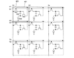
図2に、本発明の駆動方法を用いて表示を行なう発光装置の、画素部の構成を示す。図2に示すように、画素部には複数の画素200がマトリクス状に設けられており、各画素200への各種信号、電位の供給は、信号線S1〜Sx、走査線G1〜Gy、電源線V1〜Vxを介して行なわれる。
FIG. 2 shows a structure of a pixel portion of a light emitting device that performs display using the driving method of the present invention. As shown in FIG. 2, a plurality of
各画素200には、発光素子201と、画素200へのビデオ信号の入力を制御するTFT(スイッチング用TFT)202と、発光素子201への電流の供給を制御する駆動用TFT203とが設けられている。また図2では、画素200に容量素子204を駆動用TFT203とは別個に形成しているが、本発明はこの構成に限定されない。容量素子204を駆動用TFT203とは別個に形成せずとも、駆動用TFT203のゲート電極と活性層の間に形成される容量(ゲート容量)を容量素子204として用いても良い。スイッチング用TFT202と、駆動用TFT203は共にn型のTFTである。
Each
スイッチング用TFT202は、ゲートが走査線Gj(j=1〜y)に接続されている。またスイッチング用TFT202のソースとドレインは、一方が信号線Si(i=1〜x)に、他方が駆動用TFT203のゲートに接続されている。駆動用TFT203のソースとドレインは、一方が電源線Vi(i=1〜x)に、他方が発光素子201の陽極に接続されている。容量素子204が有する2つの電極は、一方が駆動用TFT203のゲートに、他方が発光素子201の陽極に接続されている。
The switching
なお図2に示す画素の構成は、本発明の駆動方法を用いることができる発光装置の一形態に過ぎず、本発明の駆動方法を用いることができる発光装置は、図2に示す構成に限定されない。 Note that the structure of the pixel shown in FIG. 2 is only one mode of a light-emitting device that can use the driving method of the present invention, and the light-emitting device that can use the driving method of the present invention is limited to the structure shown in FIG. Not.
次に、図2に示す画素部の駆動方法について説明する。本発明の駆動方法は、書き込み期間と、逆バイアス期間と、表示期間とに分けて説明することができる。図3(A)に、書き込み期間Taと、逆バイアス期間Trと、表示期間Tdのタイミングの一例を示す。 Next, a method for driving the pixel portion illustrated in FIG. 2 will be described. The driving method of the present invention can be described by being divided into a writing period, a reverse bias period, and a display period. FIG. 3A shows an example of the timing of the writing period Ta, the reverse bias period Tr, and the display period Td.
まず、逆バイアス期間Trが開始されると、直列に接続されている駆動用TFT203と発光素子201に、逆方向バイアスの電圧が印加される。具体的には、電源線V1〜Vxに電位Vssが、発光素子201の陰極に電位Vssよりも高い電位Vddが供給される。
First, when the reverse bias period Tr is started, a reverse bias voltage is applied to the driving TFT 203 and the
そして書き込み期間Taが開始される。なお本発明の駆動方法では、逆バイアス期間Tr中に書き込み期間Taが存在する。書き込み期間Taが開始されると、走査線G1〜Gyが順に選択され、各画素のスイッチング用TFT202がオンになる。そして信号線S1〜Sxにビデオ信号が供給されると、スイッチング用TFT202を介して、駆動用TFT203のゲートに該ビデオ信号の電位Vgが供給される。
Then, the writing period Ta is started. In the driving method of the present invention, the writing period Ta exists in the reverse bias period Tr. When the writing period Ta is started, the scanning lines G1 to Gy are sequentially selected, and the switching
このとき、発光素子201は非線形素子であるため、逆方向バイアスの電圧が印加されると、発光素子201の陽極と陰極間の電圧Velは、駆動用TFT203のドレイン電圧Vdsよりも著しく大きくなる。よって、発光素子201の陽極の電位は限りなく電源線V1〜Vxの電位Vssに近くなり、電位Vssとビデオ信号の電位Vgとの間の電位差が容量素子204に蓄積され、保持される。
At this time, since the light-emitting
書き込み期間Taが終了しスイッチング用TFT202がオフすると、逆バイアス期間Trが終了し、次に、表示期間Tdが開始される。
When the writing period Ta ends and the switching
表示期間では、直列に接続されている駆動用TFT203と発光素子201に、順方向バイアスの電圧が印加される。具体的には、電源線V1〜Vxに電位Vddよりも高い電位Vdd’が、発光素子201の陰極に電位Vddが供給される。
In the display period, a forward bias voltage is applied to the driving TFT 203 and the
なお本実施の形態では、逆バイアス期間Trと表示期間Tdの両期間において陰極に供給される電位を一定に保っているが、本発明はこの構成に限定されない。逆バイアス期間Trにおいて、駆動用TFT203がオンのときに発光素子201に逆方向バイアスの電圧が印加されるようにし、表示期間Tdにおいて、駆動用TFT203がオンのときに発光素子201に順方向バイアスの電圧が印加されるようにすれば良い。
Note that in this embodiment mode, the potential supplied to the cathode is kept constant in both the reverse bias period Tr and the display period Td, but the present invention is not limited to this structure. In the reverse bias period Tr, a reverse bias voltage is applied to the
順方向バイアスの電圧が印加されると、駆動用TFT203はn型であるため、駆動用TFT203のソースが発光素子201の陽極と接続されていることになる。よって、容量素子204に保持されている、電位Vssとビデオ信号の電位Vgとの間の電位差は、そのまま駆動用TFT203のゲート電圧Vgsとなる。よって駆動用TFT203は、該ゲート電圧Vgsに見合った大きさのドレイン電流を、発光素子201に供給する。
When a forward bias voltage is applied, since the driving TFT 203 is n-type, the source of the driving TFT 203 is connected to the anode of the
図3(B)に、各期間における走査線G1〜Gyと電源線V1〜Vxのタイミングチャートを示す。同じ走査線を共有している画素を一行と見たとき、各行において書き込み期間Taは順に出現している。また各書き込み期間Taは逆バイアス期間Tr内に存在している。なお、書き込み期間Taと逆バイアス期間Trを完全に重ねることも可能であるが、逆バイアス期間Trを書き込み期間Taよりも長めに取ることで、電源線V1〜Vxの電位の変動による雑音などの影響を避けることができる。 FIG. 3B shows a timing chart of the scanning lines G1 to Gy and the power supply lines V1 to Vx in each period. When pixels sharing the same scanning line are regarded as one row, the writing period Ta appears in order in each row. Each writing period Ta exists in the reverse bias period Tr. It is possible to completely overlap the writing period Ta and the reverse bias period Tr. However, by taking the reverse bias period Tr longer than the writing period Ta, noise due to fluctuations in the potential of the power supply lines V1 to Vx, The impact can be avoided.
なお本発明において駆動用TFTはn型に限定されず、p型であっても良い。ただし駆動用TFTがp型の場合、駆動用TFTと発光素子の陰極とが接続されているものとする。 In the present invention, the driving TFT is not limited to n-type, and may be p-type. However, when the driving TFT is a p-type, it is assumed that the driving TFT and the cathode of the light emitting element are connected.
なお図3(A)では、ビデオ信号がアナログである場合の、書き込み期間と、逆バイアス期間と、表示期間のタイミングの一例を示したが、本発明においてビデオ信号はデジタルであっても良い。例えばデジタルのビデオ信号を用いて、時間階調により階調を表示する場合、図7(A)に示すように、書き込み期間Taと、逆バイアス期間Trと、表示期間Tdの各期間をデジタル信号のビットごとに設ければ良い。 Note that FIG. 3A illustrates an example of the timing of the writing period, the reverse bias period, and the display period when the video signal is analog; however, in the present invention, the video signal may be digital. For example, when a gray scale is displayed using a digital video signal, a writing period Ta, a reverse bias period Tr, and a display period Td are digital signals as shown in FIG. It may be provided for each bit.
なお本実施の形態では、画素部のTFTが、アモルファス半導体またはセミアモルファス半導体を用いている例を示したが、本発明はこの構成に限定されない。本発明の駆動方法は、画素部のTFTが多結晶半導体を用いている発光装置にも適用可能である。 Note that although an example in which an amorphous semiconductor or a semi-amorphous semiconductor is used for the TFT in the pixel portion is described in this embodiment mode, the present invention is not limited to this structure. The driving method of the present invention can also be applied to a light emitting device in which a TFT in a pixel portion uses a polycrystalline semiconductor.
本実施例では、図2に示した画素部において、電源線を走査線と並列に配置し、一つの走査線駆動回路で走査線と電源線の電位を制御する、発光装置の一形態について説明する。 In this embodiment, one mode of a light-emitting device in which power supply lines are arranged in parallel with scanning lines and the potentials of the scanning lines and the power supply lines are controlled by one scanning line driver circuit in the pixel portion shown in FIG. To do.
図4に、本実施例の発光装置における画素部400の構成を示す。図4において画素401は、図2に示した画素部と同様に、発光素子405、スイッチング用TFT402、駆動用TFT403、容量素子404とを有している。各素子の接続関係は図2に示した画素200と同じである。ただし本実施例では、電源線V1〜Vyが走査線G1〜Gyと並列に配置されている。
FIG. 4 shows a configuration of the
次に、図4に示す画素部の駆動方法について説明する。本発明の駆動方法は、書き込み期間Taと、逆バイアス期間Trと、表示期間Tdとに分けて説明することができる。図20(A)に、書き込み期間Taと、逆バイアス期間Trと、表示期間Tdのタイミングの一例を示す。また、全ての画素において逆バイアス期間Trが開始されて終了するまでのトータルの期間を、Twとして示す。 Next, a method for driving the pixel portion illustrated in FIG. 4 is described. The driving method of the present invention can be described by being divided into a writing period Ta, a reverse bias period Tr, and a display period Td. FIG. 20A shows an example of the timing of the writing period Ta, the reverse bias period Tr, and the display period Td. In addition, the total period from the start to the end of the reverse bias period Tr in all pixels is denoted as Tw.
まず、逆バイアス期間Trが開始されると、発光素子405の陰極に電位Vssよりも高い電位Vddが供給され、電源線V1〜Vyに、順に電位Vssが供給される。よって、直列に接続されている駆動用TFT403と発光素子405に、逆方向バイアスの電圧が各行の画素に順に印加されることになる。
First, when the reverse bias period Tr is started, a potential Vdd higher than the potential Vss is supplied to the cathode of the light emitting element 405, and the potential Vss is sequentially supplied to the power supply lines V1 to Vy. Therefore, a reverse bias voltage is sequentially applied to the pixels in each row to the driving
そして書き込み期間Taが開始される。なお本発明の駆動方法では、各行ごとに、書き込み期間Taが逆バイアス期間Tr中に存在している。書き込み期間Taが開始されると、走査線G1〜Gyが順に選択され、各画素のスイッチング用TFT402がオンになる。そして信号線S1〜Sxにビデオ信号が供給されると、スイッチング用TFT402を介して、駆動用TFT403のゲートに該ビデオ信号の電位Vgが供給される。
Then, the writing period Ta is started. In the driving method of the present invention, the write period Ta exists in the reverse bias period Tr for each row. When the writing period Ta is started, the scanning lines G1 to Gy are sequentially selected, and the switching
このとき、発光素子405は非線形素子であるため、逆方向バイアスの電圧が印加されると、発光素子405の陽極と陰極間の電圧Velは、駆動用TFT403のドレイン電圧Vdsよりも著しく大きくなる。よって、発光素子405の陽極の電位は限りなく電源線V1〜Vyの電位Vssに近くなり、電位Vssとビデオ信号の電位Vgとの間の電位差が容量素子404に蓄積され、保持される。
At this time, since the light-emitting element 405 is a non-linear element, when a reverse bias voltage is applied, the voltage Vel between the anode and the cathode of the light-emitting element 405 becomes significantly larger than the drain voltage Vds of the driving
書き込み期間Taが終了しスイッチング用TFT402がオフすると、逆バイアス期間Trが終了し、次に、表示期間Tdが開始される。
When the writing period Ta ends and the switching
表示期間では、直列に接続されている駆動用TFT403と発光素子405に、順方向バイアスの電圧が順に印加される。具体的には、発光素子405の陰極に電位Vddが供給され、電源線V1〜Vyに電位Vddよりも高い電位Vdd’が順に供給される。
In the display period, a forward bias voltage is sequentially applied to the driving
図4に示す発光装置では、逆バイアス期間Trと表示期間Tdの両期間において陰極に供給される電位を一定に保つ。 In the light emitting device shown in FIG. 4, the potential supplied to the cathode is kept constant in both the reverse bias period Tr and the display period Td.
順方向バイアスの電圧が印加されると、駆動用TFT403はn型であるため、駆動用TFT403のソースが発光素子405の陽極と接続されていることになる。よって、容量素子404に保持されている、電位Vssとビデオ信号の電位Vgとの間の電位差は、そのまま駆動用TFT403のゲート電圧Vgsとなる。よって駆動用TFT403は、該ゲート電圧Vgsに見合った大きさのドレイン電流を、発光素子405に供給する。
When a forward bias voltage is applied, since the driving
図20(B)に、各期間における走査線G1〜Gyと電源線V1〜Vyのタイミングチャートを示す。同じ走査線を共有している画素を一行と見たとき、各行において書き込み期間Taは順に出現している。また各書き込み期間Taは対応する逆バイアス期間Tr内に存在している。なお、書き込み期間Taと逆バイアス期間Trを完全に重ねることも可能であるが、逆バイアス期間Trを書き込み期間Taよりも長めに取ることで、電源線V1〜Vyの電位の変動による雑音などの影響を避けることができる。 FIG. 20B shows a timing chart of the scanning lines G1 to Gy and the power supply lines V1 to Vy in each period. When pixels sharing the same scanning line are regarded as one row, the writing period Ta appears in order in each row. Each writing period Ta exists in the corresponding reverse bias period Tr. Note that it is possible to completely overlap the writing period Ta and the reverse bias period Tr, but by taking the reverse bias period Tr longer than the writing period Ta, noise due to fluctuations in the potentials of the power supply lines V1 to Vy can be obtained. The impact can be avoided.
図4では、図2の場合と異なり、行ごとに逆バイアス期間Trの出現するタイミングを設定することができるので、フレーム期間に占める表示期間Tdの割合を大きくすることができる。よって、駆動回路の動作周波数を抑えることができる。 In FIG. 4, unlike the case of FIG. 2, the timing at which the reverse bias period Tr appears can be set for each row, so that the ratio of the display period Td to the frame period can be increased. Therefore, the operating frequency of the drive circuit can be suppressed.
なお図20(A)では、ビデオ信号がアナログである場合の、書き込み期間と、逆バイアス期間と、表示期間のタイミングの一例を示したが、本発明においてビデオ信号はデジタルであっても良い。例えばデジタルのビデオ信号を用いて、時間階調により階調を表示する場合、図7(B)に示すように、書き込み期間Taと、逆バイアス期間Trと、表示期間Tdの各期間をデジタル信号のビットごとに設ければ良い。 Note that FIG. 20A illustrates an example of the timing of the writing period, the reverse bias period, and the display period when the video signal is analog; however, in the present invention, the video signal may be digital. For example, in the case where gradation is displayed using a time gradation using a digital video signal, as shown in FIG. 7B, each of a writing period Ta, a reverse bias period Tr, and a display period Td is represented by a digital signal. It may be provided for each bit.
図5(A)に、図4に示した画素部400と駆動回路とを有する、発光装置の構成を示す。図5(A)において、1405は信号線S1〜Sxにビデオ信号を供給する信号線駆動回路に相当し、1406は、走査線G1〜Gy及び電源線V1〜Vyの電位を制御する走査線駆動回路に相当する。
FIG. 5A illustrates a structure of a light-emitting device including the
図5(B)に、信号線駆動回路1405の一部を示す。信号線駆動回路1405は、シフトレジスタ410と、シフトレジスタ410から出力される信号を反転させるインバータ411と、シフトレジスタ410から出力される信号とインバータ411から出力される反転した信号とに同期して、ビデオ信号をサンプリングし、信号線S1〜Sxに供給するトランスミッションゲート412とを有している。
FIG. 5B illustrates part of the signal line driver circuit 1405. The signal line driver circuit 1405 is synchronized with the shift register 410, the
図5(C)に、走査線駆動回路1406の一部を示す。走査線駆動回路1406は、シフトレジスタ415と、シフトレジスタ415から出力される信号を反転させるインバータ416、417と、パルス幅制御信号によって、インバータ416から出力される反転した信号のパルス幅を制御し、走査線G1〜Gyに供給するNOR418とを有している。インバータ417から出力された信号は、電源線V1〜Vyに供給される。
FIG. 5C illustrates part of the scan line driver circuit 1406. The scan line driver circuit 1406 controls the pulse width of the inverted signal output from the
上記構成により、1つの走査線駆動回路406で、走査線G1〜Gyと電源線V1〜Vyの電位を制御することができる。 With the above structure, one scanning line driving circuit 406 can control the potentials of the scanning lines G1 to Gy and the power supply lines V1 to Vy.
本実施例では、本発明の駆動方法を用いることができる、発光装置の画素の構成について説明する。 In this embodiment, a structure of a pixel of a light-emitting device that can use the driving method of the present invention will be described.
図6(A)に示す画素は、発光素子601と、スイッチング用TFT602と、駆動用TFT603と、発光素子601の発光を強制的に終了させるための消去用TFT604と、容量素子605とを有している。スイッチング用TFT602のゲートは第1の走査線Gaj(j=1〜y)に、ソースとドレインは一方が信号線Si(i=1〜x)に、他方が駆動用TFT603のゲートに接続されている。駆動用TFT603のソースとドレインは、一方が電源線Vj(j=1〜y)に、他方が発光素子601の陽極に接続されている。消去用TFT604のゲートは第2の走査線Gbj(j=1〜y)に接続されており、ソースとドレインは、一方が駆動用TFT603のゲートに、他方が発光素子601の陽極に接続されている。容量素子605が有する2つの電極は、一方は発光素子601の陽極に、他方は駆動用TFT603のゲートに接続されている。
A pixel illustrated in FIG. 6A includes a light-emitting element 601, a switching
書き込み期間Taにおいて消去用TFT604はオフにしておく。そして直列に接続されている駆動用TFT603と発光素子601に順方向バイアスの電圧が印加されている状態で、消去用TFT604をオンにすることで、駆動用TFT603のゲート電圧Vgsを0にすることができる。よって、駆動用TFT603をオフし、発光素子601の発光を強制的に終了させ、表示期間を終わらせることができる。
In the writing period Ta, the erasing TFT 604 is turned off. Then, the gate voltage Vgs of the driving
図6(B)に示す画素は、発光素子611と、スイッチング用TFT612と、駆動用TFT613と、発光素子611の発光を強制的に終了させるための消去用TFT614と、容量素子615とを有している。スイッチング用TFT612のゲートは第1の走査線Gaj(j=1〜y)に、ソースとドレインは一方が信号線Si(i=1〜x)に、他方が駆動用TFT613のゲートに接続されている。駆動用TFT613と消去用TFTは電源線Vj(j=1〜y)と発光素子611との間に直列に接続されている。具体的には、駆動用TFT613のソースとドレインのいずれか一方が発光素子611の陽極に、消去用TFT614のソースとドレインのいずれか一方が電源線Vjに接続されている。消去用TFT614のゲートは第2の走査線Gbj(j=1〜y)に接続されている。容量素子615が有する2つの電極は、一方は発光素子611の陽極に、他方は駆動用TFT613のゲートに接続されている。
A pixel illustrated in FIG. 6B includes a light-emitting element 611, a switching
なお図6(B)では、駆動用TFT613と電源線Vjとの間に消去用TFT614が設けられている構成を示しているが、本発明は消去用TFT614を設ける位置はこれに限定されない。例えば、消去用TFT614を発光素子611と駆動用TFT613の間に設けるようにしても良い。この場合具体的には、駆動用TFT613のソースとドレインのいずれか一方が電源線Vjに、消去用TFT614のソースとドレインのいずれか一方が発光素子611の陽極に接続される。そして容量素子615が有する2つの電極は、一方は、駆動用TFT613のソースとドレインのうち、電源線Vjに接続されている方とは異なる一方に、他方は駆動用TFT613のゲートに接続される。
Note that FIG. 6B shows a structure in which the erasing
逆バイアス期間Trと表示期間Tdにおいて、消去用TFT614はオンにしておく。そして、直列に接続されている駆動用TFT613と、消去用TFT614と、発光素子611に順方向バイアスの電圧が印加されている状態で、消去用TFT614をオフにすることで、発光素子611の発光を強制的に終了させ、表示期間を終わらせることができる。
In the reverse bias period Tr and the display period Td, the erasing
デジタルのビデオ信号を用い、図6(A)、図6(B)に示した画素で時間階調により階調を表示する場合の、書き込み期間Taと、逆バイアス期間Trと、表示期間Tdと、発光素子の発光を強制的に終了させることで出現する消去期間Teのタイミングを、図7(C)に示す。図7(C)に示すように、消去期間Teを設けることで、全ての行において書き込み期間Taが終了する前に、最初に書き込み期間が終了した行から順に表示期間Trを強制的に終了させることができる。よって、書き込み期間を短くしなくとも階調数を高くすることができ、駆動回路の動作周波数を抑えることができる。 A writing period Ta, a reverse bias period Tr, and a display period Td in the case where a gray scale is displayed by a time gray scale with the pixels shown in FIGS. 6A and 6B using a digital video signal. FIG. 7C shows the timing of the erasing period Te that appears by forcibly terminating the light emission of the light emitting element. As shown in FIG. 7C, by providing the erasing period Te, the display period Tr is forcibly ended in order from the row in which the writing period is first ended before the writing period Ta is ended in all the rows. be able to. Therefore, the number of gradations can be increased without reducing the writing period, and the operating frequency of the driver circuit can be suppressed.
なお図6(A)に示す画素の場合、消去期間Teにおいて、消去用TFT604をずっと連続してオンにしておいても良いし、消去期間Teの最初にオンにした後、残りの期間はオフにしておいても良い。一方、図6(B)に示す画素の場合、消去期間Teにおいて、消去用TFT604はずっと連続してオンにしておく。 In the case of the pixel shown in FIG. 6A, the erasing TFT 604 may be turned on continuously in the erasing period Te, or after the erasing period Te is turned on first, the remaining period is turned off. You can leave it. On the other hand, in the case of the pixel shown in FIG. 6B, the erasing TFT 604 is continuously turned on during the erasing period Te.
図6(C)に、図2に示した画素において、発光素子の陽極と電源線との間に、ダイオード接続されたTFTを設けた画素の構成を示す。図6(C)に示す画素は、発光素子621と、スイッチング用TFT622と、駆動用TFT623と、容量素子624と、整流用TFT625とを有している。スイッチング用TFT622のゲートは走査線Gj(j=1〜y)に、ソースとドレインは一方が信号線Si(i=1〜x)に、他方が駆動用TFT623のゲートに接続されている。駆動用TFT623のソースとドレインは、一方が電源線Vi(i=1〜x)に、他方が発光素子621の陽極に接続されている。整流用TFT625は、ゲートが発光素子621の陽極に接続されており、ソースとドレインが、一方は電源線Viに、他方が発光素子621の陽極に接続されている。
FIG. 6C shows a structure of the pixel shown in FIG. 2 in which a diode-connected TFT is provided between the anode of the light emitting element and the power supply line. A pixel illustrated in FIG. 6C includes a light-emitting
逆バイアス期間では、整流用TFT625はソースが電源線Viに接続され、ゲートとドレインが互いに接続されている。よって整流用TFT625はオンとなり、順方向バイアスの電流が流れるので、発光素子621の陽極の電位が、電源線Viの電位により近くなる。また表示期間では、整流用TFT625はドレインが電源線Viに接続され、ゲートとソースが互いに接続されている。よって表示期間では整流用TFT625に逆方向バイアスの電圧がかかることになるので、整流用TFT625はオフとなる。上記構成により、図6(C)に示した画素では、アナログのビデオ信号を用いて低い階調を表示する際に、駆動用TFT623のドレイン電流が低くても、発光素子621の陽極の電位を電源線Viの電位により早く近づけることができる。
In the reverse bias period, the source of the rectifying
図6(D)に、図6(A)に示した画素において、発光素子の陽極と電源線との間に、ダイオード接続されたTFTを設けた画素の構成を示す。図6(D)に示す画素は、発光素子631と、スイッチング用TFT632と、駆動用TFT633と、容量素子634と、消去用TFT635と、整流用TFT636とを有している。スイッチング用TFT632のゲートは第1の走査線Gaj(j=1〜y)に、ソースとドレインは一方が信号線Si(i=1〜x)に、他方が駆動用TFT633のゲートに接続されている。駆動用TFT633のソースとドレインは、一方は電源線Vj(j=1〜y)に、他方は発光素子631の陽極に接続されている。消去用TFT635は、ゲートが第2の走査線Gbj(j=1〜y)に接続されており、ソースとドレインは、一方が駆動用TFT633のゲートに、他方が発光素子631の陽極に接続されている。整流用TFT636は、ゲートが発光素子631の陽極に接続されており、ソースとドレインが、一方は電源線Vjに、他方が発光素子631の陽極に接続されている。
FIG. 6D illustrates a structure of a pixel in which a diode-connected TFT is provided between the anode of the light-emitting element and the power supply line in the pixel illustrated in FIG. The pixel illustrated in FIG. 6D includes a light-emitting
図6(E)に、図6(B)に示した画素において、発光素子の陽極と電源線との間に、ダイオード接続されたTFTを設けた画素の構成を示す。図6(E)に示す画素は、発光素子641と、スイッチング用TFT642と、駆動用TFT643と、容量素子644と、消去用TFT645と、整流用TFT646とを有している。スイッチング用TFT642のゲートは走査線Gaj(j=1〜y)に、ソースとドレインは一方が信号線Si(i=1〜x)に、他方が駆動用TFT643のゲートに接続されている。駆動用TFT643と消去用TFT645は直列に接続されており、消去用TFT645のソースとドレインのいずれか一方が電源線Vjに、駆動用TFT643のソースとドレインのいずれか一方が発光素子641の陽極に接続されている。整流用TFT646は、ゲートが発光素子641の陽極に接続されており、ソースとドレインが、一方は電源線Vjに、他方が発光素子641の陽極に接続されている。
FIG. 6E illustrates a structure of a pixel in which a diode-connected TFT is provided between an anode of a light-emitting element and a power supply line in the pixel illustrated in FIG. 6B. A pixel illustrated in FIG. 6E includes a light-emitting element 641, a switching
なお図6(E)では、駆動用TFT643と電源線Vjとの間に消去用TFT645が設けられている構成を示しているが、本発明は消去用TFT645を設ける位置はこれに限定されない。例えば、消去用TFT645を発光素子641と駆動用TFT643の間に設けるようにしても良い。この場合具体的には、駆動用TFT643のソースとドレインのいずれか一方が電源線Vjに、消去用TFT645のソースとドレインのいずれか一方が発光素子641の陽極に接続される。そして容量素子644が有する2つの電極は、一方は、駆動用TFT643のソースとドレインのうち、電源線Vjに接続されている方とは異なる一方に、他方は駆動用TFT643のゲートに接続される。
Note that FIG. 6E illustrates a structure in which the erasing
本発明の発光装置が有する画素の構成は、本実施例で示した構成に限定されない。 The structure of the pixel included in the light-emitting device of the present invention is not limited to the structure shown in this embodiment.
本発明の発光装置では、セミアモルファス半導体で形成されたTFT(セミアモルファスTFT)を用いる場合、駆動回路を画素部と同じ基板上に形成することができる。またアモルファス半導体で形成されたTFT(アモルファスTFT)を用いる場合、別の基板に形成された駆動回路を、画素部と同じ基板上に実装しても良い。 In the light-emitting device of the present invention, in the case where a TFT (semi-amorphous TFT) formed using a semi-amorphous semiconductor is used, the driver circuit can be formed over the same substrate as the pixel portion. In the case of using a TFT formed with an amorphous semiconductor (amorphous TFT), a driver circuit formed over another substrate may be mounted on the same substrate as the pixel portion.
図8(A)に、信号線駆動回路6013のみを別途形成し、基板6011上に形成された画素部6012と接続している素子基板の形態を示す。画素部6012及び走査線駆動回路6014は、セミアモルファスTFTを用いて形成する。セミアモルファスTFTよりも高い移動度が得られるトランジスタで信号線駆動回路を形成することで、走査線駆動回路よりも高い駆動周波数が要求される信号線駆動回路の動作を安定させることができる。なお、信号線駆動回路6013は、単結晶の半導体を用いたトランジスタ、多結晶の半導体を用いたTFT、またはSOIを用いたトランジスタであっても良い。画素部6012と、信号線駆動回路6013と、走査線駆動回路6014とに、それぞれ電源の電位、各種信号等が、FPC6015を介して供給される。
FIG. 8A illustrates a mode of an element substrate in which only the signal
なお、信号線駆動回路及び走査線駆動回路を、共に画素部と同じ基板上に形成しても良い。 Note that both the signal line driver circuit and the scan line driver circuit may be formed over the same substrate as the pixel portion.
また、駆動回路を別途形成する場合、必ずしも駆動回路が形成された基板を、画素部が形成された基板上に貼り合わせる必要はなく、例えばFPC上に張り合わせるようにしても良い。図8(B)に、信号線駆動回路6023のみを別途形成し、基板6021上に形成された画素部6022及び走査線駆動回路6024と接続している素子基板の形態を示す。画素部6022及び走査線駆動回路6024は、セミアモルファスTFTを用いて形成する。信号線駆動回路6023は、FPC6025を介して画素部6022と接続されている。画素部6022と、信号線駆動回路6023と、走査線駆動回路6024とに、それぞれ電源の電位、各種信号等が、FPC6025を介して供給される。
In the case where a driver circuit is separately formed, the substrate on which the driver circuit is formed is not necessarily attached to the substrate on which the pixel portion is formed, and may be attached to, for example, an FPC. FIG. 8B illustrates a mode of an element substrate in which only the signal
また、信号線駆動回路の一部または走査線駆動回路の一部のみを、セミアモルファスTFTを用いて画素部と同じ基板上に形成し、残りを別途形成して画素部と電気的に接続するようにしても良い。図8(C)に、信号線駆動回路が有するアナログスイッチ6033aを、画素部6032、走査線駆動回路6034と同じ基板6031上に形成し、信号線駆動回路が有するシフトレジスタ6033bを別途異なる基板に形成して貼り合わせる素子基板の形態を、図8(C)に示す。画素部6032及び走査線駆動回路6034は、セミアモルファスTFTを用いて形成する。画素部6032と、信号線駆動回路と、走査線駆動回路6034とに、それぞれ電源の電位、各種信号等が、FPC6035を介して供給される。
Further, only a part of the signal line driver circuit or a part of the scanning line driver circuit is formed on the same substrate as the pixel portion using a semi-amorphous TFT, and the rest is separately formed and electrically connected to the pixel portion. You may do it. 8C, an
図8(A)〜図8(C)に示すように、本発明の発光装置は、駆動回路の一部または全部を、画素部と同じ基板上に、セミアモルファスTFTを用いて形成することができる。 As shown in FIGS. 8A to 8C, in the light-emitting device of the present invention, part or all of the driver circuit can be formed over the same substrate as the pixel portion using a semi-amorphous TFT. it can.
また、信号線駆動回路及び走査線駆動回路を全て別途形成し、画素部が形成されている基板に実装しても良い。図8(D)に、画素部6042が形成されている基板6041上に、信号線駆動回路が形成されたチップ6043と、走査線駆動回路が形成されたチップ6044とを貼り合わせる素子基板の形態を、図8(D)に示す。画素部6042は、セミアモルファスTFTまたはアモルファスTFTを用いて形成する。画素部6042と、信号線駆動回路が形成されたチップ6043と、走査線駆動回路が形成されたチップ6044とに、それぞれ電源の電位、各種信号等が、FPC6045を介して供給される。
Alternatively, the signal line driver circuit and the scan line driver circuit may be separately formed and mounted on the substrate over which the pixel portion is formed. FIG. 8D illustrates an element substrate in which a
なお、別途形成した基板の接続方法は、特に限定されるものではなく、公知のCOG方法やワイヤボンディング方法、或いはTAB方法などを用いることができる。また接続する位置は、電気的な接続が可能であるならば、図8に示した位置に限定されない。また、コントローラ、CPU、メモリ等を別途形成し、接続するようにしても良い。 Note that a method for connecting a separately formed substrate is not particularly limited, and a known COG method, wire bonding method, TAB method, or the like can be used. Further, the connection position is not limited to the position illustrated in FIG. 8 as long as electrical connection is possible. In addition, a controller, a CPU, a memory, and the like may be separately formed and connected.
なお本発明で用いる信号線駆動回路は、シフトレジスタとアナログスイッチのみを有する形態に限定されない。シフトレジスタとアナログスイッチに加え、バッファ、レベルシフタ、ソースフォロワ等、他の回路を有していても良い。また、シフトレジスタとアナログスイッチは必ずしも設ける必要はなく、例えばシフトレジスタの代わりにデコーダ回路のような信号線の選択ができる別の回路を用いても良いし、アナログスイッチの代わりにラッチ等を用いても良い。 Note that the signal line driver circuit used in the present invention is not limited to a mode having only a shift register and an analog switch. In addition to the shift register and the analog switch, other circuits such as a buffer, a level shifter, and a source follower may be included. The shift register and the analog switch are not necessarily provided. For example, another circuit that can select a signal line such as a decoder circuit may be used instead of the shift register, or a latch or the like may be used instead of the analog switch. May be.
チップの実装方法は、特に限定されるものではなく、公知のCOG方法やワイヤボンディング方法、或いはTAB方法などを用いることができる。またチップを実装する位置は、電気的な接続が可能であるならば、図8に示した位置に限定されない。また、図8では信号線駆動回路、走査線駆動回路をチップで形成した例について示したが、コントローラ、CPU、メモリ等をチップで形成し、実装するようにしても良い。また、走査線駆動回路全体をチップで形成するのではなく、走査線駆動回路を構成している回路の一部だけを、チップで形成するようにしても良い。 The chip mounting method is not particularly limited, and a known COG method, wire bonding method, TAB method, or the like can be used. Further, the position where the chip is mounted is not limited to the position shown in FIG. 8 as long as electrical connection is possible. Further, although FIG. 8 illustrates an example in which the signal line driver circuit and the scan line driver circuit are formed using a chip, a controller, a CPU, a memory, and the like may be formed using a chip and mounted. In addition, instead of forming the entire scanning line driving circuit with a chip, only a part of the circuit constituting the scanning line driving circuit may be formed with a chip.
駆動回路などの集積回路を別途チップで形成して実装することで、全ての回路を画素部と同じ基板上に形成する場合に比べて、歩留まりを高めることができ、また各回路の特性に合わせたプロセスの最適化を容易に行なうことができる。 By forming and mounting an integrated circuit such as a driver circuit separately on a chip, the yield can be increased compared to the case where all the circuits are formed on the same substrate as the pixel portion, and the characteristics of each circuit are adjusted. The process can be easily optimized.
次に、本発明の発光装置に用いられるセミアモルファス半導体を用いたTFTの構成について説明する。図9(A)に、駆動回路に用いられるTFTの断面図と、画素部に用いられるTFTの断面図を示す。501は駆動回路に用いられるTFTの断面図に相当し、502は画素部に用いられるTFT断面図に相当し、503は該TFT502によって電流が供給される発光素子の断面図に相当する。TFT501、502は逆スタガ型(ボトムゲート型)である。
Next, the structure of a TFT using a semi-amorphous semiconductor used in the light emitting device of the present invention will be described. FIG. 9A shows a cross-sectional view of a TFT used for a driver circuit and a cross-sectional view of a TFT used for a pixel portion.
駆動回路のTFT501は、基板500上に形成されたゲート電極510と、ゲート電極510を覆っているゲート絶縁膜511と、ゲート絶縁膜511を間に挟んでゲート電極510と重なっている、セミアモルファス半導体膜で形成された第1の半導体膜512とを有している。さらにTFT501は、ソース領域またはドレイン領域として機能する一対の第2の半導体膜513と、第1の半導体膜512と第2の半導体膜513の間に設けられた第3の半導体膜514とを有している。
The
図9(A)では、ゲート絶縁膜511が2層の絶縁膜で形成されているが、本発明はこの構成に限定されない。ゲート絶縁膜511が単層または3層以上の絶縁膜で形成されていても良い。
In FIG. 9A, the
また第2の半導体膜513は、アモルファス半導体膜またはセミアモルファス半導体膜で形成されており、該半導体膜に一導電型を付与する不純物が添加されている。そして一対の第2の半導体膜513は、第1の半導体膜512のチャネルが形成される領域を間に挟んで、向かい合っている。
The
また第3の半導体膜514は、アモルファス半導体膜またはセミアモルファス半導体膜で形成されており、第2の半導体膜513と同じ導電型を有し、なおかつ第2の半導体膜513よりも導電性が低くなるような特性を有している。第3の半導体膜514はLDD領域として機能するので、ドレイン領域として機能する第2の半導体膜513の端部に集中する電界を緩和し、ホットキャリア効果を防ぐことができる。第3の半導体膜514は必ずしも設ける必要はないが、設けることでTFTの耐圧性を高め、信頼性を向上させることができる。なお、TFT501がn型である場合、第3の半導体膜514を形成する際に特にn型を付与する不純物を添加せずとも、n型の導電型が得られる。よって、TFT501がn型の場合、必ずしも第3の半導体膜514にn型の不純物を添加する必要はない。ただし、チャネルが形成される第1の半導体膜には、p型の導電性を付与する不純物を添加し、極力I型に近づくようにその導電型を制御しておく。
The
また、一対の第3の半導体膜514に接するように、配線515が形成されている。
A
画素部のTFT502は、基板500上に形成されたゲート電極520と、ゲート電極520を覆っているゲート絶縁膜511と、ゲート絶縁膜511を間に挟んでゲート電極520と重なっている、セミアモルファス半導体膜で形成された第1の半導体膜522とを有している。さらにTFT502は、ソース領域またはドレイン領域として機能する一対の第2の半導体膜523と、第1の半導体膜522と第2の半導体膜523の間に設けられた第3の半導体膜524とを有している。
The
また第2の半導体膜523は、アモルファス半導体膜またはセミアモルファス半導体膜で形成されており、該半導体膜に一導電型を付与する不純物が添加されている。そして一対の第2の半導体膜523は、第1の半導体膜522のチャネルが形成される領域を間に挟んで、向かい合っている。
The
また第3の半導体膜524は、アモルファス半導体膜またはセミアモルファス半導体膜で形成されており、第2の半導体膜523と同じ導電型を有し、なおかつ第2の半導体膜523よりも導電性が低くなるような特性を有している。第3の半導体膜524はLDD領域として機能するので、ドレイン領域として機能する第2の半導体膜523の端部に集中する電界を緩和し、ホットキャリア効果を防ぐことができる。第3の半導体膜524は必ずしも設ける必要はないが、設けることでTFTの耐圧性を高め、信頼性を向上させることができる。なお、TFT502がn型である場合、第3の半導体膜524を形成する際に特にn型を付与する不純物を添加せずとも、n型の導電型が得られる。よって、TFT502がn型の場合、必ずしも第3の半導体膜524にn型の不純物を添加する必要はない。ただし、チャネルが形成される第1の半導体膜には、p型の導電性を付与する不純物を添加し、極力I型に近づくようにその導電型を制御しておく。
The
また、一対の第3の半導体膜524に接するように、配線525が形成されている。
A
また、TFT501、502及び配線515、525を覆うように、絶縁膜からなる第1のパッシベーション膜540、第2のパッシベーション膜541が形成されている。TFT501、502を覆うパッシベーション膜は2層に限らず、単層であっても良いし、3層以上であっても良い。例えば第1のパッシベーション膜540を窒化珪素、第2のパッシベーション膜541を酸化珪素で形成することができる。窒化珪素または窒化酸化珪素でパッシベーション膜を形成することで、TFT501、502が水分や酸素などの影響により、劣化するのを防ぐことができる。
A
そして、配線525の一方は、発光素子503の陽極530に接続されている。また陽極530上に接するように、電界発光層531が、該電界発光層531に接するように陰極532が形成されている。
One end of the
チャネル形成領域を含んでいる第1の半導体膜512、522を、セミアモルファス半導体で形成することで、アモルファス半導体膜を用いたTFTに比べて高い移動度のTFTを得ることができ、よって駆動回路と画素部を同一の基板に形成することができる。
By forming the
次に、本発明の発光装置が有するTFTの、図9(A)とは異なる形態について説明する。図9(B)に、駆動回路に用いられるTFTの断面図と、画素部に用いられるTFTの断面図を示す。301は駆動回路に用いられるTFTの断面図に相当し、302は画素部に用いられるTFTと、該TFT302によって電流が供給される発光素子303の断面図に相当する。
Next, a mode different from that in FIG. 9A of the TFT included in the light-emitting device of the present invention will be described. FIG. 9B shows a cross-sectional view of a TFT used for a driver circuit and a cross-sectional view of a TFT used for a pixel portion. 301 corresponds to a cross-sectional view of a TFT used in a driver circuit, and 302 corresponds to a cross-sectional view of a TFT used in a pixel portion and a light-emitting
駆動回路のTFT301と画素部のTFT302は、基板300上に形成されたゲート電極310、320と、ゲート電極310、320を覆っているゲート絶縁膜311と、ゲート絶縁膜311を間に挟んでゲート電極310、320と重なっている、セミアモルファス半導体膜で形成された第1の半導体膜312、322とをそれぞれ有している。そして、第1の半導体膜312、322のチャネル形成領域を覆うように、絶縁膜で形成されたチャネル保護膜330、331が形成されている。チャネル保護膜330、331は、TFT301、302の作製工程において、第1の半導体膜312、322のチャネル形成領域がエッチングされてしまうのを防ぐために設ける。さらにTFT301、302は、ソース領域またはドレイン領域として機能する一対の第2の半導体膜313、323と、第1の半導体膜312、322と第2の半導体膜313、323の間に設けられた第3の半導体膜314、324とをそれぞれ有している。
The
図9(B)では、ゲート絶縁膜311が2層の絶縁膜で形成されているが、本発明はこの構成に限定されない。ゲート絶縁膜311が単層または3層以上の絶縁膜で形成されていても良い。
In FIG. 9B, the
また第2の半導体膜313、323は、アモルファス半導体膜またはセミアモルファス半導体膜で形成されており、該半導体膜に一導電型を付与する不純物が添加されている。そして一対の第2の半導体膜313、323は、第1の半導体膜312のチャネルが形成される領域を間に挟んで、向かい合っている。
The
また第3の半導体膜314、324は、アモルファス半導体膜またはセミアモルファス半導体膜で形成されており、第2の半導体膜313、323と同じ導電型を有し、なおかつ第2の半導体膜313、323よりも導電性が低くなるような特性を有している。第3の半導体膜314、324はLDD領域として機能するので、ドレイン領域として機能する第2の半導体膜313、323の端部に集中する電界を緩和し、ホットキャリア効果を防ぐことができる。第3の半導体膜314、324は必ずしも設ける必要はないが、設けることでTFTの耐圧性を高め、信頼性を向上させることができる。なお、TFT301、302がn型である場合、第3の半導体膜314、324を形成する際に特にn型を付与する不純物を添加せずとも、n型の導電型が得られる。よって、TFT301、302がn型の場合、必ずしも第3の半導体膜314、324にn型の不純物を添加する必要はない。ただし、チャネルが形成される第1の半導体膜には、p型の導電性を付与する不純物を添加し、極力I型に近づくようにその導電型を制御しておく。
The
また、一対の第3の半導体膜314、324に接するように、配線315、325が形成されている。
In addition,
また、TFT301、302及び配線315、325を覆うように、絶縁膜からなる第1のパッシベーション膜340、第2のパッシベーション膜341が形成されている。TFT301、302を覆うパッシベーション膜は2層に限らず、単層であっても良いし、3層以上であっても良い。例えば第1のパッシベーション膜340を窒化珪素、第2のパッシベーション膜341を酸化珪素で形成することができる。窒化珪素または窒化酸化珪素でパッシベーション膜を形成することで、TFT301、302が水分や酸素などの影響により、劣化するのを防ぐことができる。
A
そして、配線325の一方は、発光素子303の陽極350に接続されている。また陽極350上に接するように、電界発光層351が、該電界発光層351に接するように陰極332が形成されている。
One end of the
チャネル形成領域を含んでいる第1の半導体膜312、322を、セミアモルファス半導体で形成することで、アモルファス半導体膜を用いたTFTに比べて高い移動度のTFTを得ることができ、よって駆動回路と画素部を同一の基板に形成することができる。
By forming the
なお本実施例では、セミアモルファス半導体を用いたTFTで発光装置の駆動回路と画素部を同じ基板上に形成した例について説明したが、本発明はこの構成に限定されない。セミアモルファス半導体を用いたTFTで画素部を形成し、該画素部が形成された基板に別途形成された駆動回路を貼り付けても良い。またチャネルが形成される第1の半導体膜をアモルファス半導体で形成することができる。ただしこの場合、アモルファス半導体を用いたTFTで画素部を形成し、該画素部が形成された基板に別途形成された駆動回路を貼り付けるようにする。 Note that in this embodiment, the example in which the driving circuit of the light-emitting device and the pixel portion are formed over the same substrate using a TFT using a semi-amorphous semiconductor is described; however, the present invention is not limited to this structure. A pixel portion may be formed using a TFT using a semi-amorphous semiconductor, and a driver circuit formed separately may be attached to a substrate on which the pixel portion is formed. In addition, the first semiconductor film in which the channel is formed can be formed using an amorphous semiconductor. However, in this case, a pixel portion is formed using a TFT using an amorphous semiconductor, and a separately formed drive circuit is attached to a substrate on which the pixel portion is formed.
次に、本発明の発光装置が有する画素の構成について説明する。図10(A)に、画素の回路図の一形態を、図10(B)に図10(A)に対応する画素の断面構造の一形態を示す。 Next, a structure of a pixel included in the light emitting device of the present invention will be described. FIG. 10A illustrates one mode of a circuit diagram of a pixel, and FIG. 10B illustrates one mode of a cross-sectional structure of a pixel corresponding to FIG.
図10(A)、図10(B)において、221は画素へのビデオ信号の入力を制御するためのスイッチング用TFTに相当し、222は発光素子223への電流の供給を制御するための駆動用TFTに相当する。具体的には、スイッチング用TFT221を介して画素に入力されたビデオ信号の電位に従って、駆動用TFT222のドレイン電流が制御され、該ドレイン電流が発光素子223に供給される。なお224は、スイッチング用TFT221がオフのときに駆動用TFTのゲート電圧を保持するための容量素子に相当し、必ずしも設ける必要はない。
10A and 10B,
具体的には、スイッチング用TFT221は、ゲート電極が走査線Gj(j=1〜y)に接続されており、ソース領域とドレイン領域が、一方は信号線Si(i=1〜x)に他方は駆動用TFT222のゲートに接続されている。また駆動用TFT222のソース領域とドレイン領域は、一方が電源線Vi(i=1〜x)に、他方が発光素子223の陽極225に接続されている。容量素子224が有する2つの電極は、一方が駆動用TFT222のゲート電極に、他方が発光素子223の陽極225に接続されている。
Specifically, the switching
なお図10(A)、図10(B)では、スイッチング用TFT221が、直列に接続され、なおかつゲート電極が接続された複数のTFTが、第1の半導体膜を共有しているような構成を有する、マルチゲート構造となっている。マルチゲート構造とすることで、スイッチング用TFT221のオフ電流を低減させることができる。具体的に図10(A)、図10(B)ではスイッチング用TFT221が2つのTFTが直列に接続されたような構成を有しているが、3つ以上のTFTが直列に接続され、なおかつゲート電極が接続されたようなマルチゲート構造であっても良い。また、スイッチング用TFTは必ずしもマルチゲート構造である必要はなく、ゲート電極とチャネル形成領域が単数である通常のシングルゲート構造のTFTであっても良い。
10A and 10B, the switching
次に、本発明の発光装置の、具体的な作製方法について説明する。 Next, a specific manufacturing method of the light-emitting device of the present invention will be described.
基板710はガラスや石英などの他に、プラスチック材料を用いることができる。また、ステンレスやアルミニウムなどの金属材料の上に絶縁膜を形成したものを用いても良い。この基板710上にゲート電極及びゲート配線(走査線)を形成するための導電膜を形成する。導電膜にはクロム、モリブデン、チタン、タンタル、タングステン、アルミニウムなどの金属材料またはその合金材料を用いる。この導電膜はスパッタリング法や真空蒸着法で形成することができる。
The
導電膜をエッチング加工してゲート電極712、713を形成する。ゲート電極712、713上には第1の半導体膜や配線層を形成するので、その端部がテーパー状になるように加工することが望ましい。また導電膜を、アルミニウムを主成分とする材料で形成する場合には、エッチング加工後に陽極酸化処理などをして表面を絶縁化しておくと良い。また、図示しないがこの工程でゲート電極に接続する配線も同時に形成することができる。
第1絶縁膜714と第2絶縁膜715は、ゲート電極712、713の上層に形成することでゲート絶縁膜として機能させることができる。この場合、第1絶縁膜714として酸化珪素膜、第2絶縁膜715として窒化珪素膜を形成することが好ましい。これらの絶縁膜はグロー放電分解法やスパッタリング法で形成することができる。特に、低い成膜温度でゲートリーク電流に少ない緻密な絶縁膜を形成するには、アルゴンなどの希ガス元素を反応ガスに含ませ、形成される絶縁膜中に混入させると良い。
The first
そして、このような第1、第2絶縁膜714、715上に、第1の半導体膜716を形成する。第1の半導体膜716は、セミアモルファス半導体(SAS)で形成する。
Then, a
このSASは珪化物気体をグロー放電分解することにより得ることができる。代表的な珪化物気体としては、SiH4であり、その他にもSi2H6、SiH2Cl2、SiHCl3、SiCl4、SiF4などを用いることができる。この珪化物気体を水素、水素とヘリウム、アルゴン、クリプトン、ネオンから選ばれた一種または複数種の希ガス元素で希釈して用いることでSASの形成を容易なものとすることができる。希釈率は10倍〜1000倍の範囲で珪化物気体を希釈することが好ましい。勿論、グロー放電分解による被膜の反応生成は減圧下で行なうが、圧力は概略0.1Pa〜133Paの範囲で行なえば良い。グロー放電を形成するための電力は1MHz〜120MHz、好ましくは13MHz〜60MHzの高周波電力を供給すれば良い。基板加熱温度は300度以下が好ましく、100〜200度の基板加熱温度が推奨される。 This SAS can be obtained by glow discharge decomposition of a silicide gas. A typical silicide gas is SiH 4 , and in addition, Si 2 H 6 , SiH 2 Cl 2 , SiHCl 3 , SiCl 4 , SiF 4 and the like can be used. The formation of the SAS can be facilitated by diluting the silicide gas with one or plural kinds of rare gas elements selected from hydrogen, hydrogen and helium, argon, krypton, and neon. It is preferable to dilute the silicide gas at a dilution ratio in the range of 10 times to 1000 times. Of course, the reaction of the coating by glow discharge decomposition is performed under reduced pressure, but the pressure may be in the range of about 0.1 Pa to 133 Pa. The power for forming the glow discharge may be high frequency power of 1 MHz to 120 MHz, preferably 13 MHz to 60 MHz. The substrate heating temperature is preferably 300 ° C. or less, and a substrate heating temperature of 100 to 200 ° C. is recommended.
また、珪化物気体中に、CH4、C2H6などの炭化物気体、GeH4、GeF4などのゲルマニウム化気体を混入させて、エネルギーバンド幅を1.5〜2.4eV、若しくは0.9〜1.1eVに調節しても良い。 Further, a carbide gas such as CH 4 and C 2 H 6 and a germanium gas such as GeH 4 and GeF 4 are mixed in the silicide gas, and the energy band width is 1.5 to 2.4 eV, or 0.8. You may adjust to 9-1.1 eV.
また、SASは、価電子制御を目的とした不純物元素を意図的に添加しないときに弱いn型の電気伝導性を示す。これは、アモルファス半導体を成膜するときよりも高い電力のグロー放電を行なうため酸素が半導体膜中に混入しやすいためである。そこで、TFTのチャネル形成領域を設ける第1の半導体膜に対しては、p型を付与する不純物元素を、この成膜と同時に、或いは成膜後に添加することで、しきい値制御をすることが可能となる。p型を付与する不純物元素としては、代表的には硼素であり、B2H6、BF3などの不純物気体を1ppm〜1000ppmの割合で珪化物気体に混入させると良い。例えば、p型を付与する不純物元素としてボロンを用いる場合、該ボロンの濃度を1×10¹⁴〜6×10¹⁶atoms/cm3とすると良い。 SAS exhibits weak n-type conductivity when an impurity element for the purpose of valence electron control is not intentionally added. This is because oxygen is easily mixed into the semiconductor film because glow discharge with higher power is performed than when an amorphous semiconductor is formed. Therefore, for the first semiconductor film provided with the channel formation region of the TFT, the threshold value is controlled by adding an impurity element imparting p-type at the same time as or after the film formation. Is possible. The impurity element imparting p-type is typically boron, and an impurity gas such as B 2 H 6 or BF 3 may be mixed into the silicide gas at a rate of 1 ppm to 1000 ppm. For example, when boron is used as the impurity element imparting p-type conductivity, the concentration of boron is preferably 1 × 10 14 to 6 × 10 16 atoms / cm 3 .
次に、第2の半導体膜717、第3の半導体膜718を形成する(図11(A))。第2の半導体膜717は、価電子制御を目的とした不純物元素を意図的に添加しないで形成したものであり、第1の半導体膜716と同様にSASで形成することが好ましい。この第2の半導体膜717は、ソース及びドレインを形成する一導電型を有する第3の半導体膜718と第1の半導体膜716との間に形成することで、バッファ層(緩衝層)的な働きを持っている。従って、弱n型の電気伝導性を持って第1の半導体膜716に対して、同じ導電型で一導電型を有する第3の半導体膜718を形成する場合には必ずしも必要ない。しきい値制御をする目的において、p型を付与する不純物元素を添加する場合には、第2の半導体膜717は段階的に不純物濃度を変化させる効果を持ち、接合形成を良好にする上で好ましい形態となる。すなわち、形成されるTFTにおいては、チャネル形成領域とソースまたはドレイン領域の間に形成される低濃度不純物領域(LDD領域)としての機能を持たせることが可能となる。
Next, a
一導電型を有する第3の半導体膜718はnチャネル型のTFTを形成する場合には、代表的な不純物元素としてリンを添加すれば良く、珪化物気体にPH3などの不純物気体を加えれば良い。一導電型を有する第3の半導体膜718は、価電子制御がされていることを除けば、SASのような半導体、非晶質半導体で形成されるものである。
The
以上、第1絶縁膜714から一導電型を有する第3の半導体膜718までは大気に触れさせることなく連続して形成することが可能である。すなわち、大気成分や大気中に浮遊する汚染不純物元素に汚染されることなく各積層界面を形成することができるので、TFT特性のばらつきを低減することができる。
As described above, the first insulating
次に、フォトレジストを用いてマスク719を形成し、第1の半導体膜716、第2の半導体膜717、一導電型を有する第3の半導体膜718をエッチングして島状に分離形成する(図11(B))。
Next, a
その後、ソース及びドレインに接続する配線を形成するための第2導電膜720を形成する。第2導電膜720はアルミニウム、またはアルミニウムを主成分とする導電性材料で形成するが、半導体膜と接する側の層をチタン、タンタル、モリブデン、タングステン、銅またはこれらの元素の窒化物で形成した積層構造としても良い。例えば1層目がTaで2層目がW、1層目がTaNで2層目がAl、1層目がTaNで2層目がCu、1層目がTiで2層目がAlで3層目がTiといった組み合わせも考えられる。また1層目と2層目のいずれか一方にAgPdCu合金を用いても良い。W、AlとSiの合金(Al−Si)、TiNを順次積層した3層構造としてもよい。Wの代わりに窒化タングステンを用いてもよいし、AlとSiの合金(Al−Si)に代えてAlとTiの合金膜(Al−Ti)を用いてもよいし、TiNに代えてTiを用いてもよい。アルミニウムには耐熱性を向上させるためにチタン、シリコン、スカンジウム、ネオジウム、銅などの元素を0.5〜5原子%添加させても良い(図11(C))。
After that, a second
次にマスク721を形成する。マスク721はソースおよびドレインと接続する配線を形成するためにパターン形成されたマスクであり、同時に一導電型を有する第3の半導体膜718を取り除きチャネル形成領域を形成するためのエッチングマスクとして併用されるものである。アルミニウムまたはこれを主成分とする導電膜のエチングはBCl3、Cl2などの塩化物気体を用いて行なえば良い。このエッチング加工で配線723〜726を形成する。また、チャネル形成領域を形成するためのエッチングにはSF6、NF3、CF4などのフッ化物気体を用いてエッチングを行なうが、この場合には下地となる第1の半導体膜716とのエッチング選択比をとれないので、処理時間を適宜調整して行なうこととなる。以上のようにして、チャネルエッチ型のTFTの構造を形成することができる(図12(A))。
Next, a
次に、チャネル形成領域の保護を目的とした第3絶縁膜727を、窒化珪素膜で形成する。この窒化珪素膜はスパッタリング法やグロー放電分解法で形成可能であるが、大気中に浮遊する有機物や金属物、水蒸気などの汚染不純物の侵入を防ぐためのものであり、緻密な膜であることが要求される。第3絶縁膜727に窒化珪素膜を用いることで、第1の半導体膜716中の酸素濃度を5×10¹⁹atoms/cm3以下、好ましくは1×1019atoms/cm3以下に抑えることができる。この目的において、珪素をターゲットとして、窒素とアルゴンなどの希ガス元素を混合させたスパッタガスで高周波スパッタリングされた窒化珪素膜で、膜中の希ガス元素を含ませることにより緻密化が促進されることとなる。また、グロー放電分解法においても、珪化物気体をアルゴンなどの希ガス元素で100倍〜500倍に希釈して形成された窒化珪素膜は、100度以下の低温においても緻密な膜を形成可能であり好ましい。さらに必要があれば第4絶縁膜728を酸化珪素膜で積層形成しても良い。第3絶縁膜727と第4絶縁膜728はパッシベーション膜に相当する。
Next, a third
第3絶縁膜727および/または第4絶縁膜728上には、好ましい形態として平坦化膜729を形成する。平坦化膜は、アクリル、ポリイミド、ポリアミドなどの有機樹脂、またはシロキサン系材料を出発材料として形成されたSi−O結合とSi−CHx結晶手を含む絶縁膜で形成することが好ましい。これらの材料は含水性があるので、水分の侵入及び放出を防ぐバリア膜として第6絶縁膜730を併設することが好ましい。第6絶縁膜730としては上述のような窒化珪素膜を適用すれば良い(図12(B))。
On the third
配線732は、第6絶縁膜730、平坦化膜729、第3絶縁膜727、第4絶縁膜728にコンタクトホールを形成した後に形成する(図12(C))。
The
以上のようにして形成されたチャネルエッチ型のTFTは、SASでチャネル形成領域を構成することにより2〜10cm2/V・secの電界効果移動度を得ることができる。 The channel-etched TFT formed as described above can obtain a field effect mobility of 2 to 10 cm 2 / V · sec by forming a channel formation region with SAS.
次に図13(A)に示すように、配線732に接するように、第6絶縁膜730上に陽極731を形成する。陽極731として、ITO、IZO、ITSOの他、酸化インジウムに2〜20%の酸化亜鉛(ZnO)を混合した透明導電膜を用いることができる。陽極731として上記透明導電膜の他に、窒化チタン膜またはチタン膜を用いても良い。この場合、透明導電膜を成膜した後に、窒化チタン膜またはチタン膜を、光が透過する程度の膜厚(好ましくは、5nm〜30nm程度)で成膜する。図13(A)では、陽極731としITOを用いている。陽極731は、その表面が平坦化されるように、CMP法、ポリビニルアルコール系の多孔質体で拭浄し、研磨しても良い。またCMP法を用いた研磨後に、陽極731の表面に紫外線照射、酸素プラズマ処理などを行ってもよい。
Next, as illustrated in FIG. 13A, an
次に、第6絶縁膜730上に、有機樹脂膜、無機絶縁膜またはシロキサンを用いて形成された隔壁733を形成する。なおシロキサンとは、シリコン(Si)と酸素(O)との結合で骨格構造が構成され、置換基に少なくとも水素を含む材料である。また上記構成に加えて、置換基にフッ素、アルキル基、または芳香族炭化水素のうち少なくとも1種を有していても良い。隔壁733は開口部を有しており、該開口部において陽極731が露出している。次に図13(B)に示すように、隔壁733の開口部において陽極731と接するように、電界発光層734を形成する。電界発光層734は、単数の層で構成されていても、複数の層が積層されるように構成されていてもどちらでも良い。複数の層で構成されている場合、陽極731上に、ホール注入層、ホール輸送層、発光層、電子輸送層、電子注入層の順に積層する。
Next, a
そして電界発光層734を覆うように、陰極735を形成する。陰極735は、仕事関数が小さい公知の材料、例えば、Ca、Al、CaF、MgAg、AlLi等を用いることができる。隔壁733の開口部において、陽極731と電界発光層734と陰極735が重なり合うことで、発光素子736が形成されている(図13(B))。
Then, a
なお実際には、図13まで完成したら、さらに外気に曝されないように気密性が高く、脱ガスの少ない保護フィルム(ラミネートフィルム、紫外線硬化樹脂フィルム等)やカバー材でパッケージング(封入)することが好ましい。 In actuality, when completed up to FIG. 13, packaging (encapsulation) with a protective film (laminate film, UV curable resin film, etc.) or cover material with high air tightness and low outgassing so as not to be exposed to the outside air. Is preferred.
このような、画素部と駆動回路で同じTFTを用いた素子基板は、ゲート電極形成用マスク、半導体領域形成用マスク、配線形成用マスク、コンタクトホール形成用マスク、陽極形成用マスクの合計5枚のマスクで形成することができる。 There are a total of five element substrates using the same TFT in the pixel portion and the drive circuit, including a gate electrode formation mask, a semiconductor region formation mask, a wiring formation mask, a contact hole formation mask, and an anode formation mask. The mask can be formed.
なお本実施例では、セミアモルファス半導体を用いたTFTで発光装置の駆動回路と画素部を同じ基板上に形成した例について説明したが、本発明はこの構成に限定されない。アモルファス半導体を用いたTFTで画素部を形成し、該画素部が形成された基板に別途形成された駆動回路を貼り付けても良い。 Note that in this embodiment, the example in which the driving circuit of the light-emitting device and the pixel portion are formed over the same substrate using a TFT using a semi-amorphous semiconductor is described; however, the present invention is not limited to this structure. A pixel portion may be formed using a TFT using an amorphous semiconductor, and a driver circuit which is separately formed may be attached to a substrate on which the pixel portion is formed.
なお、図11〜図13は、図9(A)に示した構成を有するTFTの作製方法について示したが、図9(B)に示した構成を有するTFTも同様に作製することができる。ただし、図9(B)に示したTFTの場合は、ゲート電極310、320に重畳させて、SASで形成された第1の半導体膜312、322上にチャネル保護膜330、331を形成する点で、図11〜図13と異なっている。
Note that FIGS. 11 to 13 illustrate a method for manufacturing a TFT having the structure illustrated in FIG. 9A; however, a TFT having the structure illustrated in FIG. 9B can be similarly manufactured. However, in the case of the TFT shown in FIG. 9B,
また、図12(A)と図12(B)では、第3絶縁膜(第1のパッシベーション膜)、第4絶縁膜(第2のパッシベーション膜)にコンタクトホールを形成した後、陽極を形成し、隔壁を形成したものである。隔壁は、アクリル、ポリイミド、ポリアミドなどの有機樹脂、またはシロキサン系材料を出発材料として形成されたSi−O結合とSi−CHx結晶手を含む絶縁膜で形成すれば良く、特に感光性の材料を用い、陽極上に開口部を形成し、その開口部の側壁が連続した曲率を持って形成される傾斜面となるように形成することが好ましい。 In FIGS. 12A and 12B, contact holes are formed in the third insulating film (first passivation film) and the fourth insulating film (second passivation film), and then an anode is formed. A partition wall is formed. The partition wall may be formed of an insulating film including an Si-O bond and an Si-CHx crystal hand formed using an organic resin such as acrylic, polyimide, or polyamide, or a siloxane-based material as a starting material. It is preferable to form an opening on the anode so that the side wall of the opening is an inclined surface formed with a continuous curvature.
本実施例では、図10に示した画素の、上面図の一実施例について説明する。 In this example, an example of a top view of the pixel shown in FIG. 10 will be described.
図14に本実施例の画素の上面図を示す。Siは信号線、Viは電源線に相当し、Gjは走査線に相当する。本実施例では、信号線Siと、電源線Viは同じ導電膜で形成する。また、走査線Gjと配線250は同じ導電膜で形成する。走査線Gjの一部は、スイッチング用TFT221のゲート電極として機能する。配線250は、その一部が駆動用TFT222のゲート電極として機能し、別の一部が容量素子224の第1の電極として機能する。また、駆動用TFT222が有する活性層の、陽極225側の一部251は、容量素子224の第2の電極として機能する。活性層の陽極225側の一部251と、配線250の一部と、ゲート絶縁膜(図示せず)とによって、容量素子224が形成される。225は陽極に相当し、電界発光層や陰極(共に図示せず)と重なる領域(発光エリア)において発光する。
FIG. 14 shows a top view of the pixel of this embodiment. Si corresponds to a signal line, Vi corresponds to a power supply line, and Gj corresponds to a scanning line. In this embodiment, the signal line Si and the power supply line Vi are formed of the same conductive film. Further, the scanning line Gj and the
なお本発明の上面図は本の一実施例であり、本発明はこれに限定されないことは言うまでもない。 The top view of the present invention is an example of the present invention, and the present invention is not limited to this.
本発明の発光装置で用いるセミアモルファスTFTまたはアモルファスTFTは、n型である。本実施例では、駆動用TFTがn型の場合を例に挙げて、画素の断面構造について説明する。 The semi-amorphous TFT or amorphous TFT used in the light emitting device of the present invention is n-type. In this embodiment, a cross-sectional structure of a pixel will be described with an example in which a driving TFT is an n-type.
図15(A)に、駆動用TFT7001がn型で、発光素子7002から発せられる光が陰極7003側に抜ける場合の、画素の断面図を示す。図15(A)では、駆動用TFT7001と電気的に接続された陽極7005上に、電界発光層7004、陰極7003が順に積層されている。陽極7005には、光を透過しにくい材料を用いることが望ましい。例えば、窒化チタンまたはチタンを用いることができる。電界発光層7004は、単数の層で構成されていても、複数の層が積層されるように構成されていてもどちらでも良い。陰極7003は、仕事関数が小さい導電膜であれば公知の材料を用いることができる。例えば、Ca、Al、CaF、MgAg、AlLi等が望ましい。ただしその膜厚は、光を透過する程度(好ましくは、5nm〜30nm程度)とする。例えば20nmの膜厚を有するAlを、陰極7003として用いることができる。そして陰極7003を覆うように透明導電膜7007を形成する。透明導電膜7007は、例えば、ITO、IZO、ITSOの他、酸化インジウムに2〜20%の酸化亜鉛(ZnO)を混合した透明導電膜を用いることができる。
FIG. 15A is a cross-sectional view of a pixel in the case where the driving
陰極7003と、電界発光層7004と、陽極7005とが重なっている部分が発光素子7002に相当する。図15(A)に示した画素の場合、発光素子7002から発せられる光は、白抜きの矢印で示すように陰極7003側に抜ける。
A portion where the cathode 7003, the electroluminescent layer 7004, and the anode 7005 overlap corresponds to the
図15(B)に、駆動用TFT7011がn型で、発光素子7012から発せられる光が陰極7013側に抜ける場合の、画素の断面図を示す。図15(B)では、発光素子7012の陽極7015と駆動用TFT7011が電気的に接続されており、陽極7015上に電界発光層7014、陰極7013が順に積層されている。陽極7015は光を透過する透明導電膜を用いて形成し、例えばITO、IZO、ITSOの他、酸化インジウムに2〜20%の酸化亜鉛(ZnO)を混合した透明導電膜を用いても良い。そして電界発光層7014は、図15(A)と同様に、単数の層で構成されていても、複数の層が積層されるように構成されていてもどちらでも良い。陰極7013は仕事関数が小さく、図15(A)の場合と同様に、仕事関数が小さい導電膜で、なおかつ光を反射する導電膜であれば公知の材料を用いることができる。
FIG. 15B is a cross-sectional view of a pixel in the case where the driving
陽極7015と、電界発光層7014と、陰極7013とが重なっている部分が発光素子7012に相当する。図15(B)に示した画素の場合、発光素子7012から発せられる光は、白抜きの矢印で示すように陽極7015側に抜ける。
A portion where the anode 7015, the electroluminescent layer 7014, and the cathode 7013 overlap corresponds to the
次に図15(C)を用いて、駆動用TFT7021がn型で、発光素子7022から発せられる光が陽極7025側と陰極7023側の両方から抜ける場合の、画素の断面図を示す。図15(C)では、駆動用TFT7021と電気的に接続された陽極7025上に、電界発光層7024、陰極7023が順に積層されている。陽極7025は、図15(B)と同様に、光を透過する透明導電膜を用いて形成することができる。そして電界発光層7024は、図15(A)と同様に、単数の層で構成されていても、複数の層が積層されるように構成されていてもどちらでも良い。陰極7023は、図15(A)の場合と同様に、仕事関数が小さい導電膜であれば公知の材料を用いることができる。ただしその膜厚は、光を透過する程度とする。例えば20nmの膜厚を有するAlを、陰極7023として用いることができる。
Next, FIG. 15C is a cross-sectional view of a pixel in the case where the driving
陰極7023と、電界発光層7024と、陽極7025とが重なっている部分が発光素子7022に相当する。図15(C)に示した画素の場合、発光素子7022から発せられる光は、白抜きの矢印で示すように陽極7025側と陰極7023側の両方に抜ける。
A portion where the cathode 7023, the electroluminescent layer 7024, and the
なお本実施例では、駆動用TFTと発光素子が電気的に接続されている例を示したが、駆動用TFTと発光素子との間に他のTFTが直列に接続されていてもよい。 Note that in this embodiment, an example in which the driving TFT and the light emitting element are electrically connected is shown, but another TFT may be connected in series between the driving TFT and the light emitting element.
なお、図15(A)〜図15(C)に示す全ての画素において、発光素子を覆うように保護膜を成膜しても良い。保護膜は水分や酸素などの発光素子の劣化を促進させる原因となる物質を、他の絶縁膜と比較して透過させにくい膜を用いる。代表的には、例えばDLC膜、窒化炭素膜、RFスパッタ法で形成された窒化珪素膜等を用いるのが望ましい。また上述した水分や酸素などの物質を透過させにくい膜と、該膜に比べて水分や酸素などの物質を透過させやすい膜とを積層させて、保護膜として用いることも可能である。 Note that a protective film may be formed so as to cover the light-emitting element in all the pixels illustrated in FIGS. 15A to 15C. As the protective film, a film that hardly transmits a substance that causes deterioration of the light-emitting element, such as moisture or oxygen, as compared with other insulating films is used. Typically, it is desirable to use, for example, a DLC film, a carbon nitride film, a silicon nitride film formed by an RF sputtering method, or the like. In addition, the above-described film that hardly transmits a substance such as moisture or oxygen and a film that easily allows a substance such as moisture or oxygen to pass through can be stacked to be used as a protective film.
また、図15(B)、図15(C)において、陰極側から光を得るためには、陰極の膜厚を薄くする方法の他に、Liを添加することで仕事関数が小さくなったITOを用いる方法もある。 In FIGS. 15B and 15C, in order to obtain light from the cathode side, in addition to the method of reducing the film thickness of the cathode, ITO whose work function is reduced by adding Li. There is also a method using.
なお本発明の発光装置は、図15に示した構成に限定されるものではなく、本発明の技術的思想に基づく各種の変形が可能である。 Note that the light emitting device of the present invention is not limited to the configuration shown in FIG. 15, and various modifications based on the technical idea of the present invention are possible.
本実施例では、極性が全て同一のTFTを用いた、シフトレジスタの一形態について説明する。図16(A)に、本実施例のシフトレジスタの構成を示す。図16(A)に示すシフトレジスタは、第1のクロック信号CLK、第2のクロック信号CLKb、スタートパルス信号SPを用いて動作する。1401はパルス出力回路であり、その具体的な構成を、図16(B)に示す。
In this embodiment, an example of a shift register using TFTs having the same polarity will be described. FIG. 16A shows the structure of the shift register of this embodiment. The shift register illustrated in FIG. 16A operates using the first clock signal CLK, the second clock signal CLKb, and the start pulse signal SP.
パルス出力回路1401は、TFT801〜806と、容量素子807を有する。TFT801は、ゲートがノード2に、ソースがTFT805のゲートに接続されており、ドレインに電位Vddが与えられている。TFT802は、ゲートがTFT806のゲートに、ドレインがTFT805のゲートに接続されており、ソースに電位Vssが与えられている。TFT803は、ゲートがノード3に、ソースがTFT806のゲートに接続されており、ドレインに電位Vddが与えられている。TFT804は、ゲートがノード2に、ドレインがTFT805のゲートに接続されており、ソースに電位Vssが与えられている。TFT805は、ゲートが容量素子807の一方の電極に、ドレインがノード1に、ソースが容量素子807の他方の電極及びノード4に接続されている。またTFT806は、ゲートが容量素子807の一方の電極に、ドレインがノード4に接続されており、ソースに電位Vssが与えられている。
The
次に、図16(B)に示すパルス出力回路1401の動作について説明する。ただし、CLK、CLKb、SPは、HレベルのときVdd、LレベルのときVssとし、さらに説明を簡単にするためVss=0と仮定する。
Next, operation of the
SPがHレベルになると、TFT801がオンになるため、TFT805のゲートの電位が上昇していく。そして最終的には、TFT805のゲートの電位がVdd−Vth(VthはTFT801〜806のしきい値とする)となったところで、TFT801がオフし、浮遊状態となる。一方、SPがHレベルになるとTFT804がオンになるため、TFT802、806のゲートの電位は下降し、最終的にはVssとなり、TFT802、806はオフになる。TFT803のゲートは、このときLレベルとなっており、オフしている。
When SP becomes H level, the
次にSPはLレベルとなり、TFT801、804がオフし、TFT805のゲートの電位がVdd−Vthで保持される。ここで、TFT805のゲート・ソース間電圧がそのしきい値Vthを上回っていれば、TFT805がオンする。
Next, SP becomes L level, the
次に、ノード1に与えられているCLKがLレベルからHレベルに変わると、TFT805がオンしているので、ノード4、すなわちTFT805のソースの電位が上昇を始める。そしてTFT805のゲート・ソース間には容量素子807による容量結合が存在しているため、ノード4の電位上昇に伴い、浮遊状態となっているTFT805のゲートの電位が再び上昇する。最終的には、TFT805のゲートの電位は、Vdd+Vthよりも高くなり、ノード4の電位はVddに等しくなる。そして、上述の動作を2段目以降のパルス出力回路1401において同様行なわれ、順にパルスが出力される。
Next, when the CLK applied to the
本実施例では、本発明の発光装置の一形態に相当するパネルの外観について、図17を用いて説明する。図17(A)は、第1の基板上に形成されたTFT及び発光素子を、第2の基板との間にシール材によって封止した、パネルの上面図であり、図17(B)は、図17(A)のA−A’における断面図に相当する。 In this example, the appearance of a panel corresponding to one embodiment of the light-emitting device of the present invention will be described with reference to FIG. FIG. 17A is a top view of a panel in which a TFT and a light-emitting element formed over a first substrate are sealed with a sealant between the second substrate and FIG. 17B. FIG. 17A corresponds to a cross-sectional view taken along the line AA ′ of FIG.
第1の基板4001上に設けられた画素部4002と、走査線駆動回路4004とを囲むようにして、シール材4005が設けられている。また画素部4002と、走査線駆動回路4004の上に第2の基板4006が設けられている。よって画素部4002と、走査線駆動回路4004とは、第1の基板4001とシール材4005と第2の基板4006とによって、充填材4007と共に密封されている。また第1の基板4001上のシール材4005によって囲まれている領域とは異なる領域に、別途用意された基板上に多結晶半導体膜で形成された信号線駆動回路4003が実装されている。なお本実施例では、多結晶半導体膜を用いたTFTを有する信号線駆動回路を、第1の基板4001に貼り合わせる例について説明するが、単結晶半導体を用いたトランジスタで信号線駆動回路を形成し、貼り合わせるようにしても良い。図17では、信号線駆動回路4003に含まれる、多結晶半導体膜で形成されたTFT4009を例示する。
A sealant 4005 is provided so as to surround the pixel portion 4002 provided over the
また第1の基板4001上に設けられた画素部4002と、走査線駆動回路4004は、TFTを複数有しており、図17(B)では、画素部4002に含まれるTFT4010とを例示している。なお本実施例では、TFT4010が駆動用TFTであると仮定する。TFT4010はセミアモルファス半導体を用いたTFTに相当する。
In addition, the pixel portion 4002 provided over the
また4011は発光素子に相当し、発光素子4011が有する画素電極は、TFT4010のドレインと、配線4017を介して電気的に接続されている。そして本実施例では、発光素子4011の対向電極と透明導電膜4012が電気的に接続されている。なお発光素子4011の構成は、本実施の形態に示した構成に限定されない。発光素子4011から取り出す光の方向や、TFT4010の極性などに合わせて、発光素子4011の構成は適宜変えることができる。
また、別途形成された信号線駆動回路4003と、走査線駆動回路4004または画素部4002に与えられる各種信号及び電位は、図17(B)に示す断面図では図示されていないが、引き回し配線4014及び4015を介して、接続端子4016から供給されている。
In addition, a variety of signals and potentials are supplied to the signal line driver circuit 4003 which is formed separately, the scan line driver circuit 4004, or the pixel portion 4002, although they are not shown in the cross-sectional view in FIG. And 4015 through a
本実施例では、接続端子4016が、発光素子4011が有する画素電極と同じ導電膜から形成されている。また、引き回し配線4014は、配線4017と同じ導電膜から形成されている。また引き回し配線4015は、TFT4010が有するゲート電極と、同じ導電膜から形成されている。
In this embodiment, the
接続端子4016は、FPC4018が有する端子と、異方性導電膜4019を介して電気的に接続されている。
The
なお、第1の基板4001、第2の基板4006としては、ガラス、金属(代表的にはステンレス)、セラミックス、プラスチックを用いることができる。プラスチックとしては、FRP(Fiberglass−Reinforced Plastics)板、PVF(ポリビニルフルオライド)フィルム、マイラーフィルム、ポリエステルフィルムまたはアクリル樹脂フィルムを用いることができる。また、アルミニウムホイルをPVFフィルムやマイラーフィルムで挟んだ構造のシートを用いることもできる。
Note that as the
但し、発光素子4011からの光の取り出し方向に位置する基板には、第2の基板は透明でなければならない。その場合には、ガラス板、プラスチック板、ポリエステルフィルムまたはアクリルフィルムのような透光性を有する材料を用いる。
However, the second substrate must be transparent to the substrate positioned in the light extraction direction from the
また、充填材4007としては窒素やアルゴンなどの不活性な気体の他に、紫外線硬化樹脂または熱硬化樹脂を用いることができ、PVC(ポリビニルクロライド)、アクリル、ポリイミド、エポキシ樹脂、シリコン樹脂、PVB(ポリビニルブチラル)またはEVA(エチレンビニルアセテート)を用いることができる。本実施例では充填材として窒素を用いた。 As the filler 4007, in addition to an inert gas such as nitrogen or argon, an ultraviolet curable resin or a thermosetting resin can be used. PVC (polyvinyl chloride), acrylic, polyimide, epoxy resin, silicon resin, PVB (Polyvinyl butyral) or EVA (ethylene vinyl acetate) can be used. In this example, nitrogen was used as the filler.
なお図17では、信号線駆動回路4003を別途形成し、第1の基板4001に実装している例を示しているが、本実施例はこの構成に限定されない。走査線駆動回路を別途形成して実装しても良いし、信号線駆動回路の一部または走査線駆動回路の一部のみを別途形成して実装しても良い。
Note that although FIG. 17 illustrates an example in which the signal line driver circuit 4003 is separately formed and mounted on the
なお本実施例では、セミアモルファス半導体を用いたTFTで発光装置の駆動回路と画素部を同じ基板上に形成した例について説明したが、本発明はこの構成に限定されない。アモルファス半導体を用いたTFTで画素部を形成し、該画素部が形成された基板に別途形成された駆動回路を貼り付けても良い。 Note that in this embodiment, the example in which the driving circuit of the light-emitting device and the pixel portion are formed over the same substrate using a TFT using a semi-amorphous semiconductor is described; however, the present invention is not limited to this structure. A pixel portion may be formed using a TFT using an amorphous semiconductor, and a driver circuit which is separately formed may be attached to a substrate on which the pixel portion is formed.
本実施例は、他の実施例に記載した構成と組み合わせて実施することが可能である。 This embodiment can be implemented in combination with the structure described in other embodiments.
発光素子を用いた発光装置は自発光型であるため、液晶ディスプレイに比べ、明るい場所での視認性に優れ、視野角が広い。従って、様々な電子機器の表示部に用いることができる。 Since a light-emitting device using a light-emitting element is a self-luminous type, it has excellent visibility in a bright place and a wide viewing angle compared to a liquid crystal display. Therefore, it can be used for display portions of various electronic devices.
本発明の発光装置を用いた電子機器として、ビデオカメラ、デジタルカメラ、ゴーグル型ディスプレイ(ヘッドマウントディスプレイ)、ナビゲーションシステム、音響再生装置(カーオーディオ、オーディオコンポ等)、ノート型パーソナルコンピュータ、ゲーム機器、携帯情報端末(モバイルコンピュータ、携帯電話、携帯型ゲーム機または電子書籍等)、記録媒体を備えた画像再生装置(具体的にはDVD:Digital Versatile Disc)等の記録媒体を再生し、その画像を表示しうるディスプレイを備えた装置)などが挙げられる。特に携帯用電子機器の場合、斜め方向から画面を見る機会が多く、視野角の広さが重要視されるため、発光装置を用いることが望ましい。また本発明では、半導体膜の成膜後に結晶化の工程を設ける必要がないので、比較的パネルの大型化が容易であるため、10〜50インチの大型のパネルを用いた電子機器に非常に有用である。それら電子機器の具体例を図18に示す。 As an electronic device using the light emitting device of the present invention, a video camera, a digital camera, a goggle type display (head mounted display), a navigation system, a sound reproduction device (car audio, audio component, etc.), a notebook type personal computer, a game device, Play back a recording medium such as a portable information terminal (mobile computer, mobile phone, portable game machine or electronic book), an image playback device (specifically a DVD: Digital Versatile Disc) equipped with a recording medium, and display the image. A device having a display capable of displaying). In particular, in the case of a portable electronic device, it is desirable to use a light-emitting device because there are many opportunities to see the screen from an oblique direction and the wide viewing angle is important. In the present invention, since it is not necessary to provide a crystallization step after the formation of the semiconductor film, it is relatively easy to increase the size of the panel. Therefore, the present invention is very suitable for an electronic device using a large panel of 10-50 inches. Useful. Specific examples of these electronic devices are shown in FIGS.
図18(A)は表示装置であり、筐体2001、支持台2002、表示部2003、スピーカー部2004、ビデオ入力端子2005等を含む。本発明の発光装置を表示部2003に用いることで、本発明の表示装置が完成する。発光装置は自発光型であるためバックライトが必要なく、液晶ディスプレイよりも薄い表示部とすることができる。なお、発光素子表示装置は、パソコン用、TV放送受信用、広告表示用などの全ての情報表示用表示装置が含まれる。
FIG. 18A illustrates a display device, which includes a
図18(B)はノート型パーソナルコンピュータであり、本体2201、筐体2202、表示部2203、キーボード2204、外部接続ポート2205、ポインティングマウス2206等を含む。本発明の発光装置を表示部2203に用いることで、本発明のノート型パーソナルコンピュータが完成する。
FIG. 18B shows a laptop personal computer, which includes a
図18(C)は記録媒体を備えた携帯型の画像再生装置(具体的にはDVD再生装置)であり、本体2401、筐体2402、表示部A2403、表示部B2404、記録媒体(DVD等)読み込み部2405、操作キー2406、スピーカー部2407等を含む。表示部A2403は主として画像情報を表示し、表示部B2404は主として文字情報を表示する。なお、記録媒体を備えた画像再生装置には家庭用ゲーム機器なども含まれる。本発明の発光装置を表示部A2403、B2404に用いることで、本発明の画像再生装置が完成する。
FIG. 18C illustrates a portable image reproducing device (specifically, a DVD reproducing device) provided with a recording medium, which includes a
また、発光装置は発光している部分が電力を消費するため、発光部分が極力少なくなるように情報を表示することが望ましい。従って、携帯情報端末、特に携帯電話や音響再生装置のような文字情報を主とする表示部に発光装置を用いる場合には、非発光部分を背景として文字情報を発光部分で形成するように駆動することが望ましい。 In addition, since the light emitting device consumes power in the light emitting portion, it is desirable to display information so that the light emitting portion is minimized. Therefore, when a light emitting device is used for a display unit mainly including character information, such as a portable information terminal, particularly a mobile phone or a sound reproduction device, it is driven so that character information is formed by the light emitting part with the non-light emitting part as the background. It is desirable to do.
以上の様に、本発明の適用範囲は極めて広く、あらゆる分野の電子機器に用いることが可能である。また、本実施例の電子機器は、実施例1〜10に示したいずれの構成の発光装置を用いても良い。
As described above, the applicable range of the present invention is so wide that it can be used for electronic devices in various fields. In addition, the electronic device of this embodiment may use the light-emitting device having any configuration shown in
Claims (6)
前記第1のTFTのソース及びドレインの一方は、信号線に電気的に接続され、
前記第1のTFTのソース及びドレインの他方は、前記第2のTFTのゲートに電気的に接続され、
前記第1のTFTのゲートは、走査線に電気的に接続され、
前記第2のTFTのソース及びドレインの一方は、電源線に電気的に接続され、
前記第2のTFTのソース及びドレインの他方は、前記発光素子の陽極に電気的に接続され、
前記容量素子の一方の電極は、前記第2のTFTのゲートに電気的に接続され、
前記容量素子の他方の電極は、前記第2のTFTのソース及びドレインの他方に電気的に接続され、
第1の期間において前記第1のTFTがオンとなり、前記第1のTFTを介して前記信号線から画像情報を有する第1の電位が前記第2のTFTのゲートに供給されるとともに、前記電源線から前記第2のTFTのソース及びドレインの一方に第2の電位が供給され、前記発光素子の陰極に第3の電位が供給されることにより、前記第1の電位と前記第2の電位との電位差を前記容量素子により保持し、
第2の期間において前記第1のTFTがオフとなるとともに、前記第2のTFTのソース及びドレインの一方に第4の電位が供給され、前記発光素子の陰極に第5の電位が供給されることにより、前記第1の電位と前記第2の電位との電位差に応じた電流が前記発光素子に供給され、
前記第2の電位は前記第3の電位よりも低く、
前記第4の電位は前記第5の電位よりも高いことを特徴とする発光装置。 Has a light emitting element, a n-type first TFT of an n-type second TFT of a pixel portion in which pixels constituted are arranged in matrix in a capacitor,
One of the source and the drain of the first TFT is electrically connected to the signal line,
The other of the source and drain of the first TFT is electrically connected to the gate of the second TFT,
A gate of the first TFT is electrically connected to a scanning line;
One of the source and the drain of the second TFT is electrically connected to a power supply line,
The other of the source and drain of the second TFT is electrically connected to the anode of the light emitting element,
One electrode of the capacitive element is electrically connected to the gate of the second TFT,
The other electrode of the capacitive element is electrically connected to the other of the source and drain of the second TFT,
In the first period, the first TFT is turned on, and a first potential having image information is supplied from the signal line to the gate of the second TFT via the first TFT, and the power source A second potential is supplied from a line to one of a source and a drain of the second TFT, and a third potential is supplied to the cathode of the light emitting element, whereby the first potential and the second potential are supplied. Is held by the capacitive element,
In the second period, the first TFT is turned off, the fourth potential is supplied to one of the source and the drain of the second TFT, and the fifth potential is supplied to the cathode of the light emitting element. Thus, a current corresponding to the potential difference between the first potential and the second potential is supplied to the light emitting element,
The second potential is lower than the third potential;
The light-emitting device, wherein the fourth potential is higher than the fifth potential.
前記第1のTFTのソース及びドレインの一方は、信号線に電気的に接続され、
前記第1のTFTのソース及びドレインの他方は、前記第2のTFTのゲートに電気的に接続され、
前記第1のTFTのゲートは、走査線に電気的に接続され、
前記第2のTFTのソース及びドレインの一方は、電源線に電気的に接続され、
前記第2のTFTのソース及びドレインの他方は、前記発光素子の陰極に電気的に接続され、
前記容量素子の一方の電極は、前記第2のTFTのゲートに電気的に接続され、
前記容量素子の他方の電極は、前記第2のTFTのソース及びドレインの他方に電気的に接続され、
第1の期間において前記第1のTFTがオンとなり、前記第1のTFTを介して前記信号線から画像情報を有する第1の電位が前記第2のTFTのゲートに供給されるとともに、前記電源線から前記第2のTFTのソース及びドレインの一方に第2の電位が供給され、前記発光素子の陽極に第3の電位が供給されることにより、前記第1の電位と前記第2の電位との電位差を前記容量素子により保持し、
第2の期間において前記第1のTFTがオフとなるとともに、前記第2のTFTのソース及びドレインの一方に第4の電位が供給され、前記発光素子の陽極に第5の電位が供給されることにより、前記第1の電位と前記第2の電位との電位差に応じた電流が前記発光素子に供給され、
前記第2の電位は前記第3の電位よりも高く、
前記第4の電位は前記第5の電位よりも低いことを特徴とする発光装置。 Has a light emitting element, a n-type first TFT of a p-type second TFT of a pixel portion in which pixels constituted are arranged in matrix in a capacitor,
One of the source and the drain of the first TFT is electrically connected to the signal line,
The other of the source and drain of the first TFT is electrically connected to the gate of the second TFT,
A gate of the first TFT is electrically connected to a scanning line;
One of the source and the drain of the second TFT is electrically connected to a power supply line,
The other of the source and drain of the second TFT is electrically connected to the cathode of the light emitting element,
One electrode of the capacitive element is electrically connected to the gate of the second TFT,
The other electrode of the capacitive element is electrically connected to the other of the source and drain of the second TFT,
In the first period, the first TFT is turned on, and a first potential having image information is supplied from the signal line to the gate of the second TFT via the first TFT, and the power source The second potential is supplied from the line to one of the source and the drain of the second TFT, and the third potential is supplied to the anode of the light emitting element, whereby the first potential and the second potential are supplied. Is held by the capacitive element,
In the second period, the first TFT is turned off, the fourth potential is supplied to one of the source and the drain of the second TFT, and the fifth potential is supplied to the anode of the light emitting element. Thus, a current corresponding to the potential difference between the first potential and the second potential is supplied to the light emitting element,
The second potential is higher than the third potential;
The light emitting device is characterized in that the fourth potential is lower than the fifth potential.
前記第2の期間において前記第2のTFTは飽和領域で動作することを特徴とする発光装置。 In claim 1 or claim 2,
In the second period, the second TFT operates in a saturation region.
前記第3の電位と前記第5の電位は同じ高さであることを特徴とする発光装置。 In any one of Claims 1 thru | or 3,
The light emitting device, wherein the third potential and the fifth potential are the same height.
前記画像情報はアナログ信号であることを特徴とする発光装置。 In any one of Claims 1 thru | or 4,
The light-emitting device, wherein the image information is an analog signal .
Priority Applications (1)
| Application Number | Priority Date | Filing Date | Title |
|---|---|---|---|
| JP2004225146A JP4939737B2 (en) | 2003-08-08 | 2004-08-02 | Light emitting device |
Applications Claiming Priority (3)
| Application Number | Priority Date | Filing Date | Title |
|---|---|---|---|
| JP2003289569 | 2003-08-08 | ||
| JP2003289569 | 2003-08-08 | ||
| JP2004225146A JP4939737B2 (en) | 2003-08-08 | 2004-08-02 | Light emitting device |
Related Child Applications (1)
| Application Number | Title | Priority Date | Filing Date |
|---|---|---|---|
| JP2011170973A Division JP2012008582A (en) | 2003-08-08 | 2011-08-04 | Light-emitting device and electronic apparatus |
Publications (3)
| Publication Number | Publication Date |
|---|---|
| JP2005092188A JP2005092188A (en) | 2005-04-07 |
| JP2005092188A5 JP2005092188A5 (en) | 2007-09-06 |
| JP4939737B2 true JP4939737B2 (en) | 2012-05-30 |
Family
ID=34466751
Family Applications (1)
| Application Number | Title | Priority Date | Filing Date |
|---|---|---|---|
| JP2004225146A Active JP4939737B2 (en) | 2003-08-08 | 2004-08-02 | Light emitting device |
Country Status (1)
| Country | Link |
|---|---|
| JP (1) | JP4939737B2 (en) |
Cited By (1)
| Publication number | Priority date | Publication date | Assignee | Title |
|---|---|---|---|---|
| JP2015129969A (en) * | 2003-08-08 | 2015-07-16 | 株式会社半導体エネルギー研究所 | Display device and electronic apparatus |
Families Citing this family (13)
| Publication number | Priority date | Publication date | Assignee | Title |
|---|---|---|---|---|
| JP5007491B2 (en) | 2005-04-14 | 2012-08-22 | セイコーエプソン株式会社 | Electro-optical device and electronic apparatus |
| JP5240534B2 (en) * | 2005-04-20 | 2013-07-17 | カシオ計算機株式会社 | Display device and drive control method thereof |
| KR20070030620A (en) * | 2005-09-13 | 2007-03-16 | 삼성에스디아이 주식회사 | Method for depositing electrode and the organic light emitting display produced using it |
| KR101171188B1 (en) | 2005-11-22 | 2012-08-06 | 삼성전자주식회사 | Display device and driving method thereof |
| US8004481B2 (en) | 2005-12-02 | 2011-08-23 | Semiconductor Energy Laboratory Co., Ltd. | Display device and electronic device |
| JP5364235B2 (en) * | 2005-12-02 | 2013-12-11 | 株式会社半導体エネルギー研究所 | Display device |
| JP5240542B2 (en) * | 2006-09-25 | 2013-07-17 | カシオ計算機株式会社 | Display driving device and driving method thereof, and display device and driving method thereof |
| JP2008286897A (en) * | 2007-05-16 | 2008-11-27 | Sony Corp | Display device, method for driving the display device, and electronic equipment |
| JP5309470B2 (en) * | 2007-05-21 | 2013-10-09 | ソニー株式会社 | Display device, driving method thereof, and electronic apparatus |
| KR101396698B1 (en) * | 2007-08-21 | 2014-05-19 | 엘지디스플레이 주식회사 | Electro-Luminescent Pixel and Display Panel and Device having the same |
| TWI589006B (en) * | 2008-11-07 | 2017-06-21 | 半導體能源研究所股份有限公司 | Semiconductor device and manufacturing method thereof |
| US9806098B2 (en) * | 2013-12-10 | 2017-10-31 | Semiconductor Energy Laboratory Co., Ltd. | Light-emitting device |
| KR20220057900A (en) * | 2020-10-30 | 2022-05-09 | 엘지디스플레이 주식회사 | Display panel and display device using the same |
Family Cites Families (7)
| Publication number | Priority date | Publication date | Assignee | Title |
|---|---|---|---|---|
| JPH10312173A (en) * | 1997-05-09 | 1998-11-24 | Pioneer Electron Corp | Picture display device |
| JP2000268957A (en) * | 1999-03-18 | 2000-09-29 | Sanyo Electric Co Ltd | Electroluminescence display device |
| JP2001109432A (en) * | 1999-10-06 | 2001-04-20 | Pioneer Electronic Corp | Driving device for active matrix type light emitting panel |
| JP4869497B2 (en) * | 2001-05-30 | 2012-02-08 | 株式会社半導体エネルギー研究所 | Display device |
| JP4052865B2 (en) * | 2001-09-28 | 2008-02-27 | 三洋電機株式会社 | Semiconductor device and display device |
| JP2003186437A (en) * | 2001-12-18 | 2003-07-04 | Sanyo Electric Co Ltd | Display device |
| JP2003195810A (en) * | 2001-12-28 | 2003-07-09 | Casio Comput Co Ltd | Driving circuit, driving device and driving method for optical method |
-
2004
- 2004-08-02 JP JP2004225146A patent/JP4939737B2/en active Active
Cited By (1)
| Publication number | Priority date | Publication date | Assignee | Title |
|---|---|---|---|---|
| JP2015129969A (en) * | 2003-08-08 | 2015-07-16 | 株式会社半導体エネルギー研究所 | Display device and electronic apparatus |
Also Published As
| Publication number | Publication date |
|---|---|
| JP2005092188A (en) | 2005-04-07 |
Similar Documents
| Publication | Publication Date | Title |
|---|---|---|
| JP6827094B2 (en) | Display device | |
| JP5143255B2 (en) | Light emitting device | |
| JP6737947B2 (en) | Light emitting device | |
| JP4748954B2 (en) | Liquid crystal display | |
| TWI576808B (en) | Semiconductor device and light emitting device | |
| JP3696116B2 (en) | Light emitting device | |
| JP2004361424A (en) | Element substrate, light emitting device and driving method of light emitting device | |
| JP2001242827A (en) | Electronic device | |
| JP4939737B2 (en) | Light emitting device | |
| JP4112527B2 (en) | Method for manufacturing light emitting device of system on panel type | |
| JP2004054200A (en) | Semiconductor device | |
| JP4906106B2 (en) | Light emitting device | |
| JP4043494B2 (en) | Semiconductor device |
Legal Events
| Date | Code | Title | Description |
|---|---|---|---|
| A521 | Request for written amendment filed |
Free format text: JAPANESE INTERMEDIATE CODE: A523 Effective date: 20070720 |
|
| A621 | Written request for application examination |
Free format text: JAPANESE INTERMEDIATE CODE: A621 Effective date: 20070720 |
|
| A131 | Notification of reasons for refusal |
Free format text: JAPANESE INTERMEDIATE CODE: A131 Effective date: 20110125 |
|
| A521 | Request for written amendment filed |
Free format text: JAPANESE INTERMEDIATE CODE: A523 Effective date: 20110301 |
|
| A131 | Notification of reasons for refusal |
Free format text: JAPANESE INTERMEDIATE CODE: A131 Effective date: 20110607 |
|
| A521 | Request for written amendment filed |
Free format text: JAPANESE INTERMEDIATE CODE: A523 Effective date: 20110805 |
|
| TRDD | Decision of grant or rejection written | ||
| A01 | Written decision to grant a patent or to grant a registration (utility model) |
Free format text: JAPANESE INTERMEDIATE CODE: A01 Effective date: 20120221 |
|
| A01 | Written decision to grant a patent or to grant a registration (utility model) |
Free format text: JAPANESE INTERMEDIATE CODE: A01 |
|
| A61 | First payment of annual fees (during grant procedure) |
Free format text: JAPANESE INTERMEDIATE CODE: A61 Effective date: 20120227 |
|
| FPAY | Renewal fee payment (event date is renewal date of database) |
Free format text: PAYMENT UNTIL: 20150302 Year of fee payment: 3 |
|
| R150 | Certificate of patent or registration of utility model |
Ref document number: 4939737 Country of ref document: JP Free format text: JAPANESE INTERMEDIATE CODE: R150 Free format text: JAPANESE INTERMEDIATE CODE: R150 |
|
| FPAY | Renewal fee payment (event date is renewal date of database) |
Free format text: PAYMENT UNTIL: 20150302 Year of fee payment: 3 |
|
| R250 | Receipt of annual fees |
Free format text: JAPANESE INTERMEDIATE CODE: R250 |
|
| R250 | Receipt of annual fees |
Free format text: JAPANESE INTERMEDIATE CODE: R250 |
|
| R250 | Receipt of annual fees |
Free format text: JAPANESE INTERMEDIATE CODE: R250 |
|
| R250 | Receipt of annual fees |
Free format text: JAPANESE INTERMEDIATE CODE: R250 |
|
| R250 | Receipt of annual fees |
Free format text: JAPANESE INTERMEDIATE CODE: R250 |
|
| R250 | Receipt of annual fees |
Free format text: JAPANESE INTERMEDIATE CODE: R250 |
|
| R250 | Receipt of annual fees |
Free format text: JAPANESE INTERMEDIATE CODE: R250 |
|
| R250 | Receipt of annual fees |
Free format text: JAPANESE INTERMEDIATE CODE: R250 |
|
| R250 | Receipt of annual fees |
Free format text: JAPANESE INTERMEDIATE CODE: R250 |