JP4929612B2 - Semiconductor laser device and heat sink - Google Patents
Semiconductor laser device and heat sink Download PDFInfo
- Publication number
- JP4929612B2 JP4929612B2 JP2005115118A JP2005115118A JP4929612B2 JP 4929612 B2 JP4929612 B2 JP 4929612B2 JP 2005115118 A JP2005115118 A JP 2005115118A JP 2005115118 A JP2005115118 A JP 2005115118A JP 4929612 B2 JP4929612 B2 JP 4929612B2
- Authority
- JP
- Japan
- Prior art keywords
- semiconductor laser
- water channel
- forming plate
- plate
- flow path
- Prior art date
- Legal status (The legal status is an assumption and is not a legal conclusion. Google has not performed a legal analysis and makes no representation as to the accuracy of the status listed.)
- Expired - Fee Related
Links
Images


Classifications
-
- H—ELECTRICITY
- H01—ELECTRIC ELEMENTS
- H01S—DEVICES USING THE PROCESS OF LIGHT AMPLIFICATION BY STIMULATED EMISSION OF RADIATION [LASER] TO AMPLIFY OR GENERATE LIGHT; DEVICES USING STIMULATED EMISSION OF ELECTROMAGNETIC RADIATION IN WAVE RANGES OTHER THAN OPTICAL
- H01S5/00—Semiconductor lasers
- H01S5/02—Structural details or components not essential to laser action
- H01S5/024—Arrangements for thermal management
- H01S5/02407—Active cooling, e.g. the laser temperature is controlled by a thermo-electric cooler or water cooling
- H01S5/02423—Liquid cooling, e.g. a liquid cools a mount of the laser
-
- H—ELECTRICITY
- H01—ELECTRIC ELEMENTS
- H01L—SEMICONDUCTOR DEVICES NOT COVERED BY CLASS H10
- H01L2924/00—Indexing scheme for arrangements or methods for connecting or disconnecting semiconductor or solid-state bodies as covered by H01L24/00
- H01L2924/0001—Technical content checked by a classifier
- H01L2924/0002—Not covered by any one of groups H01L24/00, H01L24/00 and H01L2224/00
-
- H—ELECTRICITY
- H01—ELECTRIC ELEMENTS
- H01S—DEVICES USING THE PROCESS OF LIGHT AMPLIFICATION BY STIMULATED EMISSION OF RADIATION [LASER] TO AMPLIFY OR GENERATE LIGHT; DEVICES USING STIMULATED EMISSION OF ELECTROMAGNETIC RADIATION IN WAVE RANGES OTHER THAN OPTICAL
- H01S5/00—Semiconductor lasers
- H01S5/02—Structural details or components not essential to laser action
- H01S5/022—Mountings; Housings
- H01S5/0235—Method for mounting laser chips
- H01S5/02355—Fixing laser chips on mounts
- H01S5/0237—Fixing laser chips on mounts by soldering
-
- H—ELECTRICITY
- H01—ELECTRIC ELEMENTS
- H01S—DEVICES USING THE PROCESS OF LIGHT AMPLIFICATION BY STIMULATED EMISSION OF RADIATION [LASER] TO AMPLIFY OR GENERATE LIGHT; DEVICES USING STIMULATED EMISSION OF ELECTROMAGNETIC RADIATION IN WAVE RANGES OTHER THAN OPTICAL
- H01S5/00—Semiconductor lasers
- H01S5/40—Arrangement of two or more semiconductor lasers, not provided for in groups H01S5/02 - H01S5/30
- H01S5/4025—Array arrangements, e.g. constituted by discrete laser diodes or laser bar
Landscapes
- Physics & Mathematics (AREA)
- Condensed Matter Physics & Semiconductors (AREA)
- General Physics & Mathematics (AREA)
- Electromagnetism (AREA)
- Optics & Photonics (AREA)
- Cooling Or The Like Of Semiconductors Or Solid State Devices (AREA)
- Semiconductor Lasers (AREA)
Description
本発明は、複数枚の板材を積層して、冷却液が通る流路が形成されたヒートシンク及びこのヒートシンクに半導体レーザ素子を実装した半導体レーザ装置に関する。詳しくは、ヒートシンクの上面全体を、半導体レーザ素子の熱膨張係数に近い材質で構成することで、排熱効率を低下させることなく、応力の発生を防ぐことができるようにしたものである。 The present invention relates to a heat sink in which a plurality of plate members are stacked and a flow path through which a coolant flows is formed, and a semiconductor laser device in which a semiconductor laser element is mounted on the heat sink. Specifically, the entire upper surface of the heat sink is made of a material close to the thermal expansion coefficient of the semiconductor laser element, so that the generation of stress can be prevented without reducing the exhaust heat efficiency.
数〜数十Wクラスの半導体レーザ装置では、高出力化、高信頼性化を実現するため水冷による冷却方式が多用されている。高い排熱効率を実現するためのヒートシンク構造として、マイクロチャネル型のヒートシンクがよく知られている。 In semiconductor laser devices of several to several tens of W class, a cooling method by water cooling is frequently used in order to realize high output and high reliability. A micro-channel heat sink is well known as a heat sink structure for realizing high heat exhaust efficiency.
マイクロチャネル型のような微細な流路構造を水路内部に形成する方法としては、エッチング等によりパターンを形成した金属薄板を積層し、拡散接合やロウ付け等により接合する方法が一般的である。このとき用いられる金属薄板としては、熱伝導率がよく加工が容易な銅が用いられる。 As a method for forming a micro channel type fine channel structure inside a water channel, a method of laminating thin metal plates formed with a pattern by etching or the like and bonding by diffusion bonding or brazing is common. As the metal thin plate used at this time, copper having good thermal conductivity and easy processing is used.
しかし、銅の熱膨張係数は17×10-6[1/k]程度であるのに対し、高出力半導体レーザで一般的なガリウム砒素基板の熱膨張係数は5.9×10-6[1/k]と大きな差があるので、半導体レーザチップをヒートシンクにハンダ付けした後、常温に冷却した際に応力を生じる。 However, the thermal expansion coefficient of copper is about 17 × 10 −6 [1 / k], whereas the thermal expansion coefficient of a gallium arsenide substrate generally used in a high-power semiconductor laser is 5.9 × 10 −6 [1. / K], a stress is generated when the semiconductor laser chip is soldered to a heat sink and then cooled to room temperature.
半導体レーザチップに応力が生じた状態で通電すると、結晶欠陥の増殖を促進しレーザの信頼性に悪影響を与えることが知られている。 It is known that if a semiconductor laser chip is energized in a state where stress is generated, the growth of crystal defects is promoted and the reliability of the laser is adversely affected.
従来、この問題を解決するため、インジウムはんだ等の軟らかいハンダ材を用いたり、半導体レーザチップに熱膨張係数の近い銅タングステン等のサブマウントをヒートシンクとレーザチップの間に挿入する技術が提案されている(例えば、特許文献1参照)。 Conventionally, in order to solve this problem, a technique has been proposed in which a soft solder material such as indium solder is used or a submount such as copper tungsten having a thermal expansion coefficient close to that of the semiconductor laser chip is inserted between the heat sink and the laser chip. (For example, refer to Patent Document 1).
しかし、半導体レーザチップの接合にインジウムはんだを用いると、長期通電時にインジウムはんだの合金化によってハンダ材が脆くなり、信頼性が低下するという問題がある。また、サブマウントをヒートシンクと半導体レーザチップの間に挿入すると、サブマウントの熱抵抗により排熱効率が低下するという問題がある。 However, when indium solder is used for joining the semiconductor laser chip, there is a problem that the solder material becomes brittle due to alloying of indium solder during long-term energization, and reliability is lowered. Further, when the submount is inserted between the heat sink and the semiconductor laser chip, there is a problem that the heat exhaust efficiency is lowered due to the thermal resistance of the submount.
また、マイクロチャネル型のヒートシンクはチップ直下の水流速度を高めることにより、高い排熱効率を実現する構造であるため、その部分では金属材料の腐食(浸食)が生じ、漏水が発生しやすいという問題がある。 In addition, since the microchannel heat sink has a structure that realizes high heat exhaust efficiency by increasing the water flow velocity directly under the chip, there is a problem that corrosion (erosion) of the metal material occurs at that portion, and water leakage is likely to occur. is there.
更に、水冷型の素子を複数組み積層したスタック型の半導体レーザ装置の場合、隣接する2つのヒートシンク間の電位差によって電気的な腐食が生じ、水路の近接する部位の減肉が生じ漏水に至るという問題がある。 Furthermore, in the case of a stacked semiconductor laser device in which a plurality of water-cooled elements are stacked, electrical corrosion occurs due to a potential difference between two adjacent heat sinks, resulting in thinning of the adjacent parts of the water channel, leading to water leakage. There's a problem.
本発明は、このような課題を解決するためになされたもので、排熱効率を低下させることなく、応力の発生を防ぐことができるようにした半導体レーザ装置及びヒートシンクを提供することを目的とする。 The present invention has been made to solve such problems, and an object of the present invention is to provide a semiconductor laser device and a heat sink that can prevent the generation of stress without reducing the exhaust heat efficiency. .
上述した課題を解決するため、本発明に係る半導体レーザ装置は、半導体レーザ素子と、上面に前記半導体レーザ素子を備えるヒートシンクと、を有し、前記ヒートシンクは、前記半導体レーザ素子と近い熱膨張係数を有し絶縁材料であるセラミックにより形成され、上面に前記半導体レーザ素子を搭載するレーザチップ搭載板と、積層する方向に貫通し前記半導体レーザ素子と対応する位置に放熱フィンを備える第1の流路を有し、前記レーザチップ搭載板より高熱伝導率を有する金属により形成され、前記レーザチップ搭載板を搭載する第1の放熱フィン形成板と、積層する方向に貫通する第1の供給流路形成穴部、第1の排出給流路形成穴部、及び前記半導体レーザ素子と対応する位置に設けられる循環流路を有し、前記セラミックにより形成され、前記第1の放熱フィン形成板を搭載する第1の流路形成板と、積層する方向に貫通する第2の供給流路形成穴部、第2の排出給流路形成穴部、及び前記半導体レーザ素子と対応する位置に放熱フィンを備える第2の流路を有し、高熱伝導率を有する前記金属により形成され、前記第1の流路形成板を搭載する第2の放熱フィン形成板と、前記セラミックにより形成され、積層する方向に貫通する第3の供給流路形成穴部と第3の排出流路形成穴部とを有し、前記セラミックにより形成され、前記第2の放熱フィン形成板を搭載する第2の流路形成板と、を備える。 In order to solve the above-described problems, a semiconductor laser device according to the present invention includes a semiconductor laser element and a heat sink including the semiconductor laser element on an upper surface, and the heat sink has a thermal expansion coefficient close to that of the semiconductor laser element. And a laser chip mounting plate on which the semiconductor laser element is mounted on the upper surface, and a heat sink fin that penetrates in the stacking direction and corresponds to the semiconductor laser element. A first heat radiation fin forming plate having a path and formed of a metal having a higher thermal conductivity than the laser chip mounting plate and mounting the laser chip mounting plate; and a first supply flow path penetrating in the stacking direction Forming a hole, a first discharge / supply channel forming hole, and a circulation channel provided at a position corresponding to the semiconductor laser element; A first flow path forming plate on which the first radiating fin forming plate is mounted, a second supply flow path forming hole portion penetrating in the stacking direction, and a second discharge / supply flow path forming hole portion. And a second heat radiation having a second flow path provided with heat radiation fins at a position corresponding to the semiconductor laser element, formed of the metal having a high thermal conductivity, and mounting the first flow path forming plate. A fin forming plate, and a third supply flow path forming hole and a third discharge flow path forming hole that are formed of the ceramic and penetrate in the stacking direction; And a second flow path forming plate on which the heat radiating fin forming plate is mounted.
本発明に係るヒートシンクは、上面に半導体レーザ素子を搭載するヒートシンクであって、前記半導体レーザ素子と近い熱膨張係数を有し絶縁材料であるセラミックにより形成され、上面に前記半導体レーザ素子を搭載するレーザチップ搭載板と、積層する方向に貫通し前記半導体レーザ素子と対応する位置に放熱フィンを備える第1の流路を有し、前記レーザチップ搭載板より高熱伝導率を有する金属により形成され、前記レーザチップ搭載板を搭載する第1の放熱フィン形成板と、積層する方向に貫通する第1の供給流路形成穴部、第1の排出給流路形成穴部、及び前記半導体レーザ素子と対応する位置に設けられる循環流路を有し、前記セラミックにより形成され、前記第1の放熱フィン形成板を搭載する第1の流路形成板と、積層する方向に貫通する第2の供給流路形成穴部、第2の排出給流路形成穴部、及び前記半導体レーザ素子と対応する位置に放熱フィンを備える第2の流路を有し、高熱伝導率を有する前記金属により形成され、前記第1の流路形成板を搭載する第2の放熱フィン形成板と、前記セラミックにより形成され、積層する方向に貫通する第3の供給流路形成穴部と第3の排出流路形成穴部とを有し、前記セラミックにより形成され、前記第2の放熱フィン形成板を搭載する第2の流路形成板と、を備える。
A heat sink according to the present invention is a heat sink on which a semiconductor laser element is mounted on an upper surface, and is formed of a ceramic that is an insulating material having a thermal expansion coefficient close to that of the semiconductor laser element, and the semiconductor laser element is mounted on an upper surface. A laser chip mounting plate, and a first flow path provided with a radiation fin at a position corresponding to the semiconductor laser element, penetrating in the stacking direction, and formed of a metal having higher thermal conductivity than the laser chip mounting plate; A first heat dissipating fin forming plate on which the laser chip mounting plate is mounted, a first supply channel forming hole, a first discharge / supply channel forming hole penetrating in the stacking direction, and the semiconductor laser element; A first flow path forming plate having a circulation flow path provided at a corresponding position, which is formed of the ceramic and on which the first heat radiation fin forming plate is mounted; A second supply flow path forming hole that penetrates in the direction, a second discharge supply flow path formation hole, and a second flow path that includes a radiation fin at a position corresponding to the semiconductor laser element, and has high heat conductivity A second heat dissipating fin forming plate on which the first flow path forming plate is mounted, and a third supply flow path forming hole formed in the ceramic and penetrating in the stacking direction. And a third discharge flow path forming hole, and is formed of the ceramic, and includes a second flow path forming plate on which the second radiation fin forming plate is mounted.
本発明に係る半導体レーザ装置では、半導体レーザ素子が駆動されることで発生する熱は、ヒートシンクに伝達される。ヒートシンクは流路を冷却液が流れることで、半導体レーザ素子から受けた熱を冷却する。これにより、半導体レーザ素子が冷却される。 In the semiconductor laser device according to the present invention, the heat generated by driving the semiconductor laser element is transmitted to the heat sink. The heat sink cools the heat received from the semiconductor laser element by flowing the coolant through the flow path. Thereby, the semiconductor laser element is cooled.
ヒートシンクは、半導体レーザ素子が実装される搭載板部が、半導体レーザ素子の熱膨張係数に近い材質で構成される。これにより、半導体レーザ素子が駆動されることで発生する熱により半導体レーザ素子及び搭載板部が伸縮する際に、半導体レーザ素子に発生する応力が低減される。 In the heat sink, the mounting plate portion on which the semiconductor laser element is mounted is made of a material close to the thermal expansion coefficient of the semiconductor laser element. Thereby, when the semiconductor laser element and the mounting plate portion expand and contract due to heat generated by driving the semiconductor laser element, stress generated in the semiconductor laser element is reduced.
本発明によれば、半導体レーザ素子に発生する熱応力が低減するので、半導体レーザ素子の信頼性を向上させることができる。また、ヒートシンクの上面全体が単一の材質で構成されるので、熱抵抗による排熱効率の低下を抑えることができる。 According to the present invention, since the thermal stress generated in the semiconductor laser element is reduced, the reliability of the semiconductor laser element can be improved. Moreover, since the whole upper surface of a heat sink is comprised with a single material, the fall of the exhaust heat efficiency by heat resistance can be suppressed.
更に、ヒートシンクにおいて半導体レーザ素子が実装される搭載板部が、半導体レーザ素子と熱膨張係数が近い例えば絶縁材料で構成されることで、流路と接する部位での腐食を抑え、漏水を防ぐことができる。 Furthermore, the mounting plate portion on which the semiconductor laser element is mounted in the heat sink is made of an insulating material having a thermal expansion coefficient close to that of the semiconductor laser element, thereby suppressing corrosion at a portion in contact with the flow path and preventing water leakage. Can do.
以下、図面を参照して本発明の半導体レーザ装置及びヒートシンクの実施の形態について説明する。 Hereinafter, embodiments of a semiconductor laser device and a heat sink according to the present invention will be described with reference to the drawings.
<第1の実施の形態の半導体レーザ装置の構成例>
図1は第1の実施の形態の半導体レーザ装置及びこの半導体レーザ装置を構成する本実施の形態のヒートシンクの構成の一例を示す分解斜視図、図2は第1の実施の形態の半導体レーザ装置の構成の一例を示す側断面図である。
<Configuration Example of Semiconductor Laser Device in First Embodiment>
FIG. 1 is an exploded perspective view showing an example of the configuration of the semiconductor laser device of the first embodiment and the heat sink of the present embodiment constituting the semiconductor laser device, and FIG. 2 is the semiconductor laser device of the first embodiment. It is a sectional side view which shows an example of a structure.
第1の実施の形態の半導体レーザ装置1Aは、マイクロチャネル型の微細流路構造を有するヒートシンク2に、半導体レーザチップ3を搭載して構成される。本実施の形態のヒートシンク2は、薄板材を積層して構成され、本例では、第1層を構成するレーザチップ搭載板4と、第2層及び第4層を構成する放熱フィン形成板5,6と、第3層及び第5層を構成する水路形成板7,8を備えた5層構造である。ヒートシンク2は、各板材が拡散接合等の方法で接合されて一体に構成される。
The semiconductor laser device 1A of the first embodiment is configured by mounting a
レーザチップ搭載板4は搭載板部の一例で、半導体レーザチップ3が搭載される薄板材であり、半導体レーザチップ3を構成する材質の熱膨張係数に近い熱膨張係数を持つ材質により形成される。半導体レーザチップ3が例えば一般的なガリウム砒素基板で構成されている場合、レーザチップ搭載板4は、コバールや銅−タングステン合金等の金属、または、窒化アルミニウム、シリコンカーバイト等のセラミックで構成される。
The laser
ここで、レーザチップ搭載板4を絶縁材料であるセラミックで構成する場合は、表面に金メッキ等でメタル層4mを形成し、半導体レーザチップ3の下面の電極と電気的なコンタクトを取れるような構成とする。
Here, when the laser
放熱フィン形成板5は流路形成板部の一例で、例えば高熱伝導率の金属で構成され、放熱フィン形成水路9を備える。放熱フィン形成板6は流路形成板部の一例で、放熱フィン形成板5と同様に、高熱伝導率の金属で構成され、放熱フィン形成水路10と供給水路形成穴部11と排出水路形成穴部12を備える。ここで、放熱フィン形成板5,6は、レーザチップ搭載板4がセラミックで構成される場合、熱伝導率が良く、かつ、セラミックに対して拡散接合できるような銅等で構成される。
The radiating
放熱フィン形成板5の放熱フィン形成水路9は、放熱フィン形成板5を上下に貫通して形成され、半導体レーザチップ3の搭載位置の下部に複数枚の放熱フィン9fが並べて配置されて、各放熱フィン9fの間を冷却水が通る構成である。
The radiating fin forming
放熱フィン形成板6の放熱フィン形成水路10は、放熱フィン形成板6を上下に貫通して形成され、放熱フィン形成水路9と同様に、半導体レーザチップ3の搭載位置の下部に複数枚の放熱フィン10fが並べて配置されて、各放熱フィン10fの間を冷却水が通る構成である。また、放熱フィン形成水路10は、放熱フィン10fに冷却水を供給する導入水路10iが一体に形成される。
The radiating fin forming
放熱フィン形成板6の供給水路形成穴部11と排出水路形成穴部12は、放熱フィン形成板6を上下に貫通し、それぞれ放熱フィン形成水路10と独立して形成される。
The supply water
水路形成板7は流路形成板部の一例で、レーザチップ搭載板4と同じ材質で構成され、循環水路13と、供給水路形成穴部14と、排出水路形成穴部15を備える。水路形成板8は流路形成板部の一例で、水路形成板7と同様に、レーザチップ搭載板4と同じ材質で構成され、供給水路形成穴部16と、排出水路形成穴部17を備える。例えば、レーザチップ搭載板4がセラミックで構成される場合、水路形成板7,8はセラミックで構成される。
The water
水路形成板7の循環水路13は、水路形成板7を上下に貫通し、上層側の放熱フィン形成板5の放熱フィン形成水路9及び下層側の放熱フィン形成板6の放熱フィン形成水路10と繋がる位置に形成される。
The
水路形成板7の供給水路形成穴部14は、水路形成板7を上下に貫通し、下層側の放熱フィン形成板6の供給水路形成穴部11及び導入水路10iと繋がる位置及び形状で形成される。
The supply water
水路形成板7の排出水路形成穴部15は、水路形成板7を上下に貫通し、上層側の放熱フィン形成板5の放熱フィン形成水路9及び下層側の放熱フィン形成板6の排出水路形成穴部12と繋がる位置に形成される。
The drainage
水路形成板8の供給水路形成穴部16は、水路形成板8を上下に貫通し、上層側の放熱フィン形成板6の供給水路形成穴部11と繋がる位置に形成される。水路形成板8の排出水路形成穴部17は、水路形成板8を上下に貫通し、上層側の放熱フィン形成板6の排出水路形成穴部12と繋がる位置に形成される。
The supply water
ヒートシンク2は、レーザチップ搭載板4と、放熱フィン形成板5と、水路形成板7と、放熱フィン形成板6と、水路形成板8が順に積層され、拡散接合等の方法により各板材が一体に接合される。
In the
これにより、放熱フィン形成板5の放熱フィン形成水路9と、放熱フィン形成板6の放熱フィン形成水路10は、水路形成板7の循環水路13を介して繋がる。また、水路形成板7の排出水路形成穴部15と、放熱フィン形成板6の排出水路形成穴部12と、水路形成板8の排出水路形成穴部17が繋がって、排出水路18が形成される。排出水路18は、放熱フィン形成板5の放熱フィン形成水路9と繋がる。
Thereby, the radiation fin forming
更に、水路形成板7の供給水路形成穴部14と、放熱フィン形成板6の供給水路形成穴部11と、水路形成板8の供給水路形成穴部16が繋がって、供給水路19が形成される。供給水路19は、放熱フィン形成板6の放熱フィン形成水路10の導入水路10iと繋がる。
Furthermore, the supply water
これにより、ヒートシンク2は、供給水路19から放熱フィン形成板6の放熱フィン形成水路10、水路形成板7の循環水路13及び放熱フィン形成板5の放熱フィン形成水路9を通り、排出水路18へと繋がる冷却水の流路20が形成される。
Thus, the
上述したように、ヒートシンク2は5層構造であるので、最上層となる第1層を構成するレーザチップ搭載板4と、中間層となる第3層を構成する水路形成板7及び最下層となる第5層を構成する水路形成板8を同じ材質とし、第2層を構成する放熱フィン形成板5と、第4層を構成する放熱フィン形成板6を同じ材質とすることで、ヒートシンク2は積層方向に対称な構成となっている。
As described above, since the
これにより、高温で拡散接合した後、常温に戻した際にも、第1層を構成するレーザチップ搭載板4、第3層及び第5層を構成する水路形成板7,8と、第2層及び第4層を構成す放熱フィン形成板5,6の熱膨張係数の差による反りが生じにくい構成となっている。
As a result, the laser
半導体レーザチップ3は半導体レーザ素子の一例で、複数の発光部が並べて配置されるアレイ構造を有する。半導体レーザチップ3は、ヒートシンク2のレーザチップ搭載板4に、ハンダ付け等の方法で実装される。
The
上述したように、レーザチップ搭載板4をセラミックで構成した場合は、レーザチップ搭載板4の表面にメタル層4mが形成され、メタル層4mと半導体レーザチップ3の下面の電極が電気的に接続される。そして、半導体レーザチップ3の上面の図示しない電極と、メタル層4mは、それぞれボンディングワイヤ等で図示しないドライバ素子と電気的に接続される。
As described above, when the laser
ここで、レーザチップ搭載板4上における半導体レーザチップ3の実装位置は、放熱フィン形成板5の放熱フィン形成水路9に形成された放熱フィン9f及び放熱フィン形成板6の放熱フィン形成水路10に形成された放熱フィン10fの上側である。
Here, the mounting position of the
上述したように、ヒートシンク2のレーザチップ搭載板4は、半導体レーザチップ3に近い熱膨張係数を持つ材質で構成されることで、レーザチップ搭載板4と半導体レーザチップ3は、熱による伸縮の割合が、略同等となる。これにより、ヒートシンク2と半導体レーザチップ3の接合を、金スズ合金等の硬いハンダ材を用いても、半導体レーザチップ3に応力が生じにくい構成となっている。
As described above, the laser
半導体レーザチップ3に生じる応力を、インジウムハンダ等の軟らかいハンダ材を用いて緩和する構成とした場合、半導体レーザチップ3に対する長期通電時にインジウムハンダの合金化によってハンダが脆くなるという問題が生じる。これに対して、本実施の形態では、半導体レーザチップ3とヒートシンク2を金スズ合金等の硬いハンダ材を用いて接合できるので、長期通電時でもハンダ材が劣化することは無く、長期間にわたって信頼性を確保することが可能となる。
When the stress generated in the
<第1の実施の形態の半導体レーザ装置の動作例>
次に、第1の実施の形態の半導体レーザ装置1Aの動作例について説明する。半導体レーザ装置1Aは、ヒートシンク2の供給水路19及び排出水路18が、冷却水の給排水を行うチラーと称される図示しない循環装置に接続される。
<Operation Example of Semiconductor Laser Device in First Embodiment>
Next, an operation example of the semiconductor laser device 1A according to the first embodiment will be described. In the semiconductor laser device 1A, the
ヒートシンク2は、供給水路19に冷却水が供給されると、供給水路19から放熱フィン形成板6の放熱フィン形成水路10、水路形成板7の循環水路13及び放熱フィン形成板5の放熱フィン形成水路9を通り、排出水路18へと繋がる流路20を冷却水が流れる。
When the cooling water is supplied to the
すなわち、供給水路19に供給された冷却水は、放熱フィン形成板6の導入水路10iから放熱フィン形成水路10に流れる。放熱フィン形成水路10を流れる冷却水は、放熱フィン10fの間を通り、水路形成板7の循環水路13から放熱フィン形成板5の放熱フィン形成水路9に流れる。放熱フィン形成水路9を流れる冷却水は、放熱フィン9fの間を通り、排出水路18から排出される。
That is, the cooling water supplied to the
半導体レーザチップ3は、図示しないドライバ素子から受けた電気信号を、光信号に変換して出力する。半導体レーザチップ3が駆動されることで発生した熱は、レーザチップ搭載板4からヒートシンク2に伝達される。ヒートシンク2は、上述したように、流路20を冷却水が流れることで、半導体レーザチップ3から受けた熱を冷却する。これにより、半導体レーザチップ3が冷却される。
The
本例のヒートシンク2では、半導体レーザチップ3の搭載位置の下部に、放熱フィン9f及び放熱フィン10fが配置され、冷却水と接する面積を拡大してあり、また、放熱フィン形成水路9等において乱流を生じさせることで、半導体レーザチップ3から受けた熱を、効率良く放熱することができる。
In the
また、マイクロチャネル型であるヒートシンク2では、半導体レーザチップ3の直下の水流速度を高めることにより、高い排熱効率を実現している。このため、半導体レーザチップ3が搭載されるレーザチップ搭載板4の下面には、水流速度の速い冷却水が当たる。
Further, in the
本例のヒートシンク2では、上面に半導体レーザチップ3が実装され、下面が冷却水と接するレーザチップ搭載板4をセラミックで構成すると共に、水路形成板7及び水路形成板8をセラミックで構成することで、水流速度の速い部分での金属腐食による減肉及び漏水は発生しない。
In the
これにより、放熱フィン形成板5及び放熱フィン形成板6を熱伝導率の良い銅等の金属で構成することで、排熱効果を高めると共に、放熱フィン形成板5及び放熱フィン形成板6には適切な腐食しろを設定することにより、ヒートシンク2全体で漏水を防止することができる。
Thus, the heat dissipating
また、半導体レーザチップ3が実装されるレーザチップ搭載板4を絶縁材料であるセラミックで構成すると共に、放熱フィン形成板5と放熱フィン形成板6の間の水路形成板7と、放熱フィン形成板6の下の水路形成板8を、絶縁材料であるセラミックで構成することで、金属で構成される放熱フィン形成板5及び放熱フィン形成板6には、半導体レーザチップ3を駆動する電流は流れない。これにより、内部抵抗による電位差による迷走電流腐食も防止することができる。
Further, the laser
更に、本例のヒートシンク2では、ヒートシンク2の上面に直接半導体レーザチップ3を硬いハンダ材で接続できるようになるため、半導体レーザチップ3の搭載位置に他の材質で構成されるサブマウントを挿入する構成に比べると、熱抵抗及び電気的抵抗を小さくできる。
Furthermore, in the
この際、ヒートシンク2の上面を構成するレーザチップ搭載板4の熱伝導率は、放熱フィン形成板5,6を構成する銅等に比べると相対的に低いものを使用することになるが、サブマウント使用時と同じ材質、厚みのものを使用すれば、少なくともサブマウント挿入時よりはトータルの熱抵抗を小さくすることができる。
At this time, the heat conductivity of the laser
<第2の実施の形態の半導体レーザ装置の構成例>
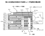
図3は第2の実施の形態の半導体レーザ装置の構成の一例を示す側断面図である。第2の実施の形態の半導体レーザ装置1Bは、第1の実施の形態の半導体レーザ装置1Aを縦方向に例えば2組積層したスタック型と呼ばれる半導体レーザ装置である。
<Configuration Example of Semiconductor Laser Device of Second Embodiment>
FIG. 3 is a side sectional view showing an example of the configuration of the semiconductor laser device according to the second embodiment. The semiconductor laser device 1B of the second embodiment is a semiconductor laser device called a stack type in which, for example, two sets of the semiconductor laser devices 1A of the first embodiment are stacked in the vertical direction.
なお、本例では半導体レーザ装置を2組積層した例を示しているが、積層段数は2組に限るものではなく、例えば20段程度積層する構成とすることで、高出力の半導体レーザ装置を実現することも可能である。 In this example, two sets of semiconductor laser devices are stacked. However, the number of stacked layers is not limited to two. For example, a configuration in which about 20 layers are stacked allows a high-power semiconductor laser device to be stacked. It can also be realized.
第2の実施の形態の半導体レーザ装置1Bは、マイクロチャネル型の微細流路構造を有する上部ヒートシンク2Aと下部ヒートシンク2Bを備え、それぞれのヒートシンク2に、半導体レーザチップ3を搭載して構成される。
A semiconductor laser device 1B according to the second embodiment includes an upper heat sink 2A and a lower heat sink 2B having a microchannel type fine channel structure, and a
図4は第2の実施の形態の半導体レーザ装置の要部構成を示す上部ヒートシンク2Aの分解斜視図である。上部ヒートシンク2Aは、図1に示す第1の実施の形態のヒートシンク2と同様の構成を有し、薄板材を積層して構成され、本例では、第1層を構成するレーザチップ搭載板4Aと、第2層及び第4層を構成する放熱フィン形成板5A,6Aと、第3層及び第5層を構成する水路形成板7A,8Aを備えた5層構造である。上部ヒートシンク2Aは、各板材が拡散接合等の方法で接合されて一体に構成される。
FIG. 4 is an exploded perspective view of the upper heat sink 2A showing the configuration of the main part of the semiconductor laser device of the second embodiment. The upper heat sink 2A has the same configuration as the
レーザチップ搭載板4Aは、半導体レーザチップ3Aを構成する材質の熱膨張係数に近い熱膨張係数を持つ材質により形成され、例えばセラミックで構成される。ここで、レーザチップ搭載板4Aを絶縁材料であるセラミックで構成する場合は、表面に金メッキ等でメタル層4mを形成し、半導体レーザチップ3Aの下面の電極と電気的なコンタクトを取れるような構成とする。 The laser chip mounting plate 4A is formed of a material having a thermal expansion coefficient close to that of the material constituting the semiconductor laser chip 3A, and is made of, for example, ceramic. Here, when the laser chip mounting plate 4A is made of ceramic which is an insulating material, a metal layer 4m is formed on the surface by gold plating or the like so that electrical contact can be made with the electrode on the lower surface of the semiconductor laser chip 3A. And
放熱フィン形成板5A及び放熱フィン形成板6Aは、高熱伝導率材料である例えば銅で構成され、放熱フィン形成板5Aは放熱フィン形成水路9Aを備え、放熱フィン形成板6Aは放熱フィン形成水路10Aと供給水路形成穴部11Aと排出水路形成穴部12Aを備える。ここで、放熱フィン形成水路9A、放熱フィン形成水路10A、供給水路形成穴部11A及び排出水路形成穴部12Aの構成は、図1で説明したヒートシンク2の各部の構成と同じである。
The radiating fin forming plate 5A and the radiating fin forming plate 6A are made of, for example, copper which is a high thermal conductivity material. The radiating fin forming plate 5A includes a radiating fin forming water channel 9A, and the radiating fin forming plate 6A is a radiating fin forming
水路形成板7Aおよび水路形成板部8Aは、レーザチップ搭載板4Aと同じ材質で構成され、水路形成板7Aは循環水路13Aと、供給水路形成穴部14Aと、排出水路形成穴部15Aを備える。また、水路形成板8Aは、供給水路形成穴部16Aと、排出水路形成穴部17Aを備える。ここで、循環水路13A、供給水路形成穴部14A及び排出水路形成穴部15Aと、供給水路形成穴部16A及び排出水路形成穴部17Aは、図1で説明したヒートシンク2の各部の構成と同じである。
The water channel forming plate 7A and the water channel forming plate portion 8A are made of the same material as the laser chip mounting plate 4A, and the water channel forming plate 7A includes a circulating
上部ヒートシンク2Aは、レーザチップ搭載板4Aに半導体レーザチップ3Aがハンダ付け等の方法で実装される。また、レーザチップ搭載板4Aは、半導体レーザチップ3Aが搭載されていない位置に、スペーサ板21が接合される。スペーサ板21は、レーザチップ搭載板4Aと同じ材質、例えばセラミックで構成され、表面に金メッキ等でメタル層21mが形成される。
In the upper heat sink 2A, the semiconductor laser chip 3A is mounted on the laser chip mounting plate 4A by a method such as soldering. The laser chip mounting plate 4A is joined to the spacer plate 21 at a position where the semiconductor laser chip 3A is not mounted. The spacer plate 21 is made of the same material as the laser chip mounting plate 4A, for example, ceramic, and a
上述したように、レーザチップ搭載板4Aをセラミックで構成した場合は、レーザチップ搭載板4Aの表面にメタル層4mが形成され、メタル層4mと半導体レーザチップ3Aの下面の電極が電気的に接続される。また、半導体レーザチップ3Aの上面の図示しない電極と、スペーサ板21のメタル層21mは、ボンディングワイヤ22で接続される。
As described above, when the laser chip mounting plate 4A is made of ceramic, the metal layer 4m is formed on the surface of the laser chip mounting plate 4A, and the metal layer 4m and the electrode on the lower surface of the semiconductor laser chip 3A are electrically connected. Is done. Further, an electrode (not shown) on the upper surface of the
図5は第2の実施の形態の半導体レーザ装置の要部構成を示す下部ヒートシンク2Bの分解斜視図である。下部ヒートシンク2Bは、上部ヒートシンク2Aとの接続部分の構成以外は、第1の実施の形態のヒートシンク2と同様の構成を有し、薄板材を積層して構成される。
FIG. 5 is an exploded perspective view of the lower heat sink 2B showing the main configuration of the semiconductor laser device according to the second embodiment. The lower heat sink 2B has the same configuration as the
下部ヒートシンク2Bは、第1層を構成するレーザチップ搭載板4Bと、第2層及び第4層を構成する放熱フィン形成板5B,6Bと、第3層及び第5層を構成する水路形成板7B,8Bを備えた5層構造である。下部ヒートシンク2Bは、各板材が拡散接合等の方法で接合されて一体に構成される。 The lower heat sink 2B includes a laser chip mounting plate 4B constituting the first layer, radiating fin forming plates 5B and 6B constituting the second layer and the fourth layer, and a water channel forming plate constituting the third layer and the fifth layer. It is a five-layer structure with 7B and 8B. The lower heat sink 2B is configured integrally by joining the plate materials by a method such as diffusion bonding.
レーザチップ搭載板4Bは、半導体レーザチップ3Bを構成する材質の熱膨張係数に近い熱膨張係数を持つ材質、例えばセラミックで構成され、供給水路形成穴部23と排出水路形成穴部24を備える。
The laser chip mounting plate 4B is made of a material having a thermal expansion coefficient close to that of the material constituting the semiconductor laser chip 3B, for example, ceramic, and includes a supply water
レーザチップ搭載板4Bの供給水路形成穴部23と排出水路形成穴部24は、それぞれレーザチップ搭載板4Bを上下に貫通して形成され、供給水路形成穴部23は、上部ヒートシンク2Aの供給水路形成穴部16Aと繋がる位置に形成される。また、排出水路形成穴部24は、上部ヒートシンク2Aの排出水路形成穴部17Aと繋がる位置に形成される。
The supply water
ここで、レーザチップ搭載板4Bを絶縁材料であるセラミックで構成する場合は、表面に金メッキ等でメタル層4mを形成し、半導体レーザチップ3Bの下面の電極と電気的なコンタクトを取れるような構成とする。なお、供給水路形成穴部23と排出水路形成穴部24は、メタル層4mを貫通して形成される。
Here, when the laser chip mounting plate 4B is made of ceramic which is an insulating material, a metal layer 4m is formed on the surface by gold plating or the like so that electrical contact can be made with the electrode on the lower surface of the semiconductor laser chip 3B. And The supply water
放熱フィン形成板5B及び放熱フィン形成板6Bは、高熱伝導率材料である例えば銅で構成される。放熱フィン形成板5Bは、放熱フィン形成水路9Bと、供給水路形成穴部25を備える。また、放熱フィン形成板6Bは放熱フィン形成水路10Bと供給水路形成穴部11Bと排出水路形成穴部12Bを備える。
The radiating fin forming plate 5B and the radiating fin forming plate 6B are made of, for example, copper, which is a high thermal conductivity material. The radiating fin forming plate 5B includes a radiating fin forming
放熱フィン形成板5Bの放熱フィン形成水路9Bは、放熱フィン形成板5Bを上下に貫通して形成され、半導体レーザチップ3Bの搭載位置の下部に複数枚の放熱フィン9fが並べて配置されて、各放熱フィン9fの間を冷却水が通る構成である。また、放熱フィン形成水路9Bは、上層側のレーザチップ搭載板4Bの排出水路形成穴部24と繋がる位置に形成される。
The radiating fin forming
放熱フィン形成板5Bの供給水路形成穴部25は、放熱フィン形成板5Bを上下に貫通し、上層側のレーザチップ搭載板4Bの供給水路形成孔部23と繋がる位置に形成される。
The supply water
放熱フィン形成板6Bの放熱フィン形成水路10Bは、放熱フィン形成板6Bを上下に貫通して形成され、放熱フィン形成水路9Bと同様に、半導体レーザチップ3Bの搭載位置の下部に複数枚の放熱フィン10fが並べて配置されて、各放熱フィン10fの間を冷却水が通る構成である。また、放熱フィン形成水路10Bは、放熱フィン10fに冷却水を供給する導入水路10iが一体に形成される。
The radiating fin forming
放熱フィン形成板6Bの供給水路形成穴部11Bと排出水路形成穴部12Bは、放熱フィン形成板6Bを上下に貫通し、それぞれ放熱フィン形成水路10Bと独立して形成される。
The supply water passage formation hole portion 11B and the discharge water passage
水路形成板7Bと水路形成板8Bは、レーザチップ搭載板4Bと同じ材質である例えばセラミックで構成される。水位路形成板7Bは、循環水路13Bと、供給水路形成穴部14Bと、排出水路形成穴部15Bを備える。また、水路形成板8Bは供給水路形成穴部16Bと、排出水路形成穴部17Bを備える。
The water channel forming plate 7B and the water channel forming plate 8B are made of, for example, ceramic, which is the same material as the laser chip mounting plate 4B. The water level passage forming plate 7B includes a circulation water passage 13B, a supply water
水路形成板7Bの循環水路13Bは、水路形成板7Bを上下に貫通し、上層側の放熱フィン形成板5Bの放熱フィン形成水路9B及び下層側の放熱フィン形成板6Bの放熱フィン形成水路10Bと繋がる位置に形成される。
The circulating water channel 13B of the water channel forming plate 7B penetrates the water channel forming plate 7B up and down, and the heat radiation fin forming
水路形成板7Bの供給水路形成穴部14Bは、水路形成板7Bを上下に貫通し、上層側の放熱フィン形成板5Bの循環水路形成穴部25と、下層側の放熱フィン形成板6Bの供給水路形成穴部11B及び導入水路10iと繋がる位置及び形状で形成される。
The supply water
水路形成板7Bの排出水路形成穴部15Bは、水路形成板7Bを上下に貫通し、上層側の放熱フィン形成板5Bの放熱フィン形成水路9B及び下層側の放熱フィン形成板6Bの排出水路形成穴部12Bと繋がる位置に形成される。
The drainage channel forming hole 15B of the channel forming plate 7B penetrates the channel forming plate 7B up and down, and forms the drainage channel of the radiating
水路形成板8Bの供給水路形成穴部16Bは、水路形成板8Bを上下に貫通し、上層側の放熱フィン形成板6Bの供給水路形成穴部11Bと繋がる位置に形成される。水路形成板8Bの排出水路形成穴部17Bは、水路形成板8Bを上下に貫通し、上層側の放熱フィン形成板6Bの排出水路形成穴部12Bと繋がる位置に形成される。
The supply water channel forming hole 16B of the water channel forming plate 8B penetrates the water channel forming plate 8B up and down, and is formed at a position connected to the supply water channel forming hole 11B of the upper radiating fin forming plate 6B. The discharge
ここで、下部ヒートシンク2Bにおいても、半導体レーザチップ3Bが実装されるレーザチップ搭載板4Bをセラミックで構成すると共に、積層方向に対称な構成とするために、水路形成板7Bと水路形成板8Bをセラミックで構成した場合、放熱フィン形成板5Bと放熱フィン形成板6Bは、セラミックに対して拡散接合できる高熱伝導率材料である例えば銅で構成される。 Here, also in the lower heat sink 2B, the laser chip mounting plate 4B on which the semiconductor laser chip 3B is mounted is made of ceramic, and the water channel forming plate 7B and the water channel forming plate 8B are provided in order to make the configuration symmetrical in the stacking direction. When constituted of ceramic, the radiating fin forming plate 5B and the radiating fin forming plate 6B are made of, for example, copper, which is a high thermal conductivity material that can be diffusion bonded to the ceramic.
下部ヒートシンク2Bは、レーザチップ搭載板4Bに半導体レーザチップ3Bがハンダ付け等の方法で実装される。また、レーザチップ搭載板4Bは、半導体レーザチップ3Bが搭載されていない位置に、スペーサ板26が接合される。スペーサ板26は、レーザチップ搭載板4Bと同じ材質、例えばセラミックで構成され、表面に金メッキ等でメタル層26mが形成される。
In the lower heat sink 2B, the semiconductor laser chip 3B is mounted on the laser chip mounting plate 4B by a method such as soldering. The
また、スペーサ板26は、供給水路形成穴部27と排出水路形成穴部28を備える。供給水路形成穴部27は、レーザチップ搭載板4Bの供給水路形成穴部23と繋がる位置に形成される。また、排出水路形成穴部28は、レーザチップ搭載板4Bの排出水路形成穴部24と繋がる位置に形成される。
The
上述したように、レーザチップ搭載板4Bをセラミックで構成した場合は、レーザチップ搭載板4Bの表面にメタル層4mが形成され、メタル層4mと半導体レーザチップ3Bの下面の電極が電気的に接続される。また、半導体レーザチップ3Bの上面の図示しない電極と、スペーサ板26のメタル層26mは、ボンディングワイヤ29で接続される。
As described above, when the laser chip mounting plate 4B is made of ceramic, the metal layer 4m is formed on the surface of the laser chip mounting plate 4B, and the metal layer 4m and the electrode on the lower surface of the semiconductor laser chip 3B are electrically connected. Is done. Further, an electrode (not shown) on the upper surface of the
上部ヒートシンク2Aは、レーザチップ搭載板4Aと、放熱フィン形成板5Aと、水路形成板7Aと、放熱フィン形成板6Aと、水路形成板8Aが順に積層され、拡散接合等の方法により各板材が一体に接合される。上部ヒートシンク2Aは、レーザチップ搭載板4Aにスペーサ板21が接合される。 In the upper heat sink 2A, a laser chip mounting plate 4A, a radiating fin forming plate 5A, a water channel forming plate 7A, a radiating fin forming plate 6A, and a water channel forming plate 8A are sequentially laminated, and each plate material is formed by a method such as diffusion bonding. They are joined together. In the upper heat sink 2A, the spacer plate 21 is bonded to the laser chip mounting plate 4A.
また、下部ヒートシンク2Bは、レーザチップ搭載板4Bと、放熱フィン形成板5Bと、水路形成板7Bと、放熱フィン形成板6Bと、水路形成板8Bが順に積層され、拡散接合等の方法により各板材が一体に接合される。下部ヒートシンク2Bは、レーザチップ搭載板4Bにスペーサ板26が接合される。
The lower heat sink 2B includes a laser chip mounting plate 4B, a heat radiating fin forming plate 5B, a water channel forming plate 7B, a heat radiating fin forming plate 6B, and a water channel forming plate 8B, which are laminated in order. The plate materials are joined together. In the lower heat sink 2B, a
これにより、上部ヒートシンク2Aにおいては、放熱フィン形成板5Aの放熱フィン形成水路9Aと、放熱フィン形成板6Aの放熱フィン形成水路10Aは、水路形成板7Aの循環水路13Aを介して繋がる。
As a result, in the upper heat sink 2A, the radiating fin forming water channel 9A of the radiating fin forming plate 5A and the radiating fin forming
また、水路形成板7Aの排出水路形成穴部15Aと、放熱フィン形成板6Aの排出水路形成穴部12Aと、水路形成板8Aの排出水路形成穴部17Aが繋がって、排出水路18Aが形成される。排出水路18Aは、放熱フィン形成板5Aの放熱フィン形成水路9Aと繋がる。
Further, the discharge water
更に、水路形成板7Aの供給水路形成穴部14Aと、放熱フィン形成板6Aの供給水路形成穴部11Aと、水路形成板8Aの供給水路形成穴部16Aが繋がって、供給水路19Aが形成される。供給水路19Aは、放熱フィン形成板6Aの放熱フィン形成水路10Aの導入水路10iと繋がる。
Furthermore, the supply water channel forming hole 14A of the water channel forming plate 7A, the supply water
下部ヒートシンク2Bにおいては、放熱フィン形成板5Bの放熱フィン形成水路9Bと、放熱フィン形成板6Bの放熱フィン形成水路10Bは、水路形成板7Bの循環水路13Bを介して繋がる。
In the lower heat sink 2B, the radiating fin forming
また、スペーサ板26の排出水路形成穴部28と、レーザチップ搭載板4Bの排出水路形成穴部24と、放熱フィン形成板5Bの放熱フィン形成水路9Bと、水路形成板7Bの排出水路形成穴部15Bと、放熱フィン形成板6Bの排出水路形成穴部12Bと、水路形成板8Bの排出水路形成穴部17Bが繋がって、排出水路18Bが形成される。
Further, the discharge water passage forming hole 28 of the
更に、スペーサ板26の供給水路形成穴部27と、レーザチップ搭載板4Bの供給水路形成穴部23と、放熱フィン形成板5Bの供給水路形成穴部25と、水路形成板7Bの供給水路形成穴部14Bと、放熱フィン形成板6Bの供給水路形成穴部11Bと、水路形成板8Bの供給水路形成穴部16Bが繋がって、供給水路19Bが形成される。供給水路19Bは、供給水路形成穴部14B及び導入水路10iを介して放熱フィン形成板6Bの放熱フィン形成水路10Bと繋がる。
Further, the supply water
そして、上部ヒートシンク2Aと下部ヒートシンク2Bは、排出水路18Aと排出水路18Bの間、及び供給水路19Aと供給水路19Bの間をOリング30でシールして接合され、上部ヒートシンク2Aと下部ヒートシンク2Bの間で繋がった流路31が形成される。
The upper heat sink 2A and the lower heat sink 2B are joined by sealing with an O-
上述したように、上部ヒートシンク2Aは5層構造であるので、上部ヒートシンク2Aにおいて最上層となる第1層を構成するレーザチップ搭載板4Aと、中間層となる第3層を構成する水路形成板7A及び最下層となる第5層を構成する水路形成板8Aを同じ材質とし、第2層を構成する放熱フィン形成板5Aと、第4層を構成する放熱フィン形成板6Aを同じ材質とすることで、上部ヒートシンク2Aは積層方向に対称な構成となっている。 As described above, since the upper heat sink 2A has a five-layer structure, the laser chip mounting plate 4A constituting the first layer as the uppermost layer and the water channel forming plate constituting the third layer as the intermediate layer in the upper heat sink 2A. 7A and the water channel forming plate 8A constituting the fifth layer as the lowermost layer are made of the same material, and the heat radiating fin forming plate 5A constituting the second layer and the heat radiating fin forming plate 6A constituting the fourth layer are made of the same material. Thus, the upper heat sink 2A has a symmetric configuration in the stacking direction.
また、下部ヒートシンク2Bも同様に5層構造であるので、下部ヒートシンク2Bにおいて最上層となる第1層を構成するレーザチップ搭載板4Bと、中間層となる第3層を構成する水路形成板7B及び最下層となる第5層を構成する水路形成板8Bを同じ材質とし、第2層を構成する放熱フィン形成板5Bと、第4層を構成する放熱フィン形成板6Bを同じ材質とすることで、下部ヒートシンク2Bは積層方向に対称な構成となっている。 Similarly, since the lower heat sink 2B has a five-layer structure, the laser chip mounting plate 4B constituting the first layer as the uppermost layer and the water channel forming plate 7B constituting the third layer as the intermediate layer in the lower heat sink 2B. And the water channel forming plate 8B constituting the fifth layer as the lowermost layer is made of the same material, and the heat radiating fin forming plate 5B constituting the second layer and the heat radiating fin forming plate 6B constituting the fourth layer are made of the same material. Thus, the lower heat sink 2B is symmetric in the stacking direction.
これにより、上部ヒートシンク2Aと下部ヒートシンク2Bは、高温で拡散接合した後、常温に戻した際にも、各層を構成する板材の熱膨張係数の差による反りが生じにくい構成となっている。 As a result, the upper heat sink 2A and the lower heat sink 2B are configured to be less likely to warp due to the difference in thermal expansion coefficients of the plate materials constituting each layer even when the heat sink is diffused and bonded at a high temperature and then returned to room temperature.
半導体レーザ装置1Bにおける半導体レーザチップ3の電気的な接続は、上部ヒートシンク2Aにおいて半導体レーザチップ3Aの図示しない上部電極と接続されるスペーサ板21のメタル層21mが、ドライバ素子32等の電源に接続される。また、下部ヒートシンク2Bにおいて半導体レーザチップ3Bの図示しない下部電極と接続されるレーザチップ搭載板4Bのメタル層4mが、ドライバ素子32等の電源に接続される。
The electrical connection of the
更に、上部ヒートシンク2Aにおいて半導体レーザチップ3Aの図示しない下部電極と接続されるレーザチップ搭載板4Aのメタル層4mと、下部ヒートシンク2Bにおいて半導体レーザチップ3Bの図示しない上部電極と接続されるスペーサ板26のメタル層26mの間が、ボンディングワイヤ33で接続される。
Further, the metal layer 4m of the laser chip mounting plate 4A connected to the lower electrode (not shown) of the semiconductor laser chip 3A in the upper heat sink 2A, and the
これにより、上下の半導体レーザチップ3に、ドライバ素子32から直列に電流が供給される構成である。
Thus, the current is supplied in series from the
ここで、上部ヒートシンク2Aのレーザチップ搭載板4Aは、半導体レーザチップ3Aに近い熱膨張係数を持つ材質で構成されることで、半導体レーザチップ3Aの接合に金スズ合金等の硬いハンダ材を用いても、半導体レーザチップ3Aに応力が生じにくい構成となっている。これにより、長期通電時でもハンダ材が劣化することは無く、長期間にわたって信頼性を確保することが可能となる。 Here, the laser chip mounting plate 4A of the upper heat sink 2A is made of a material having a thermal expansion coefficient close to that of the semiconductor laser chip 3A, so that a hard solder material such as a gold-tin alloy is used to join the semiconductor laser chip 3A. However, the semiconductor laser chip 3A is less likely to be stressed. As a result, the solder material does not deteriorate even during long-term energization, and reliability can be ensured over a long period of time.
同様に、下部ヒートシンク2Bのレーザチップ搭載板4Bは、半導体レーザチップ3Bに近い熱膨張係数を持つ材質で構成されることで、半導体レーザチップ3Bの接合に金スズ合金等の硬いハンダ材を用いても、半導体レーザチップ3Bに応力が生じにくい構成となっている。これにより、長期通電時でもハンダ材が劣化することは無く、長期間にわたって信頼性を確保することが可能となる。 Similarly, the laser chip mounting plate 4B of the lower heat sink 2B is made of a material having a thermal expansion coefficient close to that of the semiconductor laser chip 3B, so that a hard solder material such as a gold-tin alloy is used to join the semiconductor laser chip 3B. However, the semiconductor laser chip 3B has a configuration in which stress is hardly generated. As a result, the solder material does not deteriorate even during long-term energization, and reliability can be ensured over a long period of time.
<第2の実施の形態の半導体レーザ装置の動作例>
次に、第2の実施の形態の半導体レーザ装置1Bの動作例について説明する。半導体レーザ装置1Bは、下部ヒートシンク2Bの供給水路19B及び排出水路18Bが、冷却水の給排水を行う図示しない循環装置に接続される。
<Operation Example of Semiconductor Laser Device of Second Embodiment>
Next, an operation example of the semiconductor laser device 1B of the second embodiment will be described. In the semiconductor laser device 1B, the supply water channel 19B and the discharge water channel 18B of the lower heat sink 2B are connected to a circulation device (not shown) that supplies and discharges cooling water.
下部ヒートシンク2Bの供給水路19Bに冷却水が供給されると、一部の冷却水は、放熱フィン形成板6Bの導入水路10iから放熱フィン形成水路10Bへ流れる。放熱フィン形成水路10Bを流れる冷却水は、放熱フィン10fの間を通り、水路形成板7Bの循環水路13Bから放熱フィン形成板5Bの放熱フィン形成水路9Bに流れる。放熱フィン形成水路9Bを流れる冷却水は、放熱フィン9fの間を通り、排出水路18Bから排出される。
When the cooling water is supplied to the supply water channel 19B of the lower heat sink 2B, a part of the cooling water flows from the introduction water channel 10i of the radiating fin forming plate 6B to the radiating fin forming
下部ヒートシンク2Bの供給水路19Bに冷却水が供給されると、一部の冷却水は、供給水路19Bを通過して、上部ヒートシンク2Aの供給水路19Aに供給される。上部ヒートシンク2Aの供給水路19Aに冷却水が供給されると、放熱フィン形成板6Aの導入水路10iから放熱フィン形成水路10Aへ流れる。放熱フィン形成水路10Aを流れる冷却水は、放熱フィン10fの間を通り、水路形成板7Aの循環水路13Aから放熱フィン形成板5Aの放熱フィン形成水路9Aに流れる。放熱フィン形成水路9Aを流れる冷却水は、放熱フィン9fの間を通り、排出水路18Aから下部ヒートシンク2Bの排出水路18Bへと排出され、排出水路18Bから排出される。
When the cooling water is supplied to the supply water channel 19B of the lower heat sink 2B, a part of the cooling water passes through the supply water channel 19B and is supplied to the supply water channel 19A of the upper heat sink 2A. When cooling water is supplied to the supply water channel 19A of the upper heat sink 2A, it flows from the introduction water channel 10i of the radiating fin forming plate 6A to the radiating fin forming
半導体レーザチップ3A及び半導体レーザチップ3Bは、ドライバ素子32から受けた電気信号を、光信号に変換して出力する。なお、上下の半導体レーザチップ3A,3Bから出力された光信号は、図示しないレンズで集光されて、例えば光ファイバに入射させることで、高出力の光信号を得ることができる。
The semiconductor laser chip 3A and the semiconductor laser chip 3B convert the electrical signal received from the
半導体レーザチップ3Aが駆動されることで発生した熱は、レーザチップ搭載板4Aから上部ヒートシンク2Aに伝達される。上部ヒートシンク2Aでは、上述したように、流路31を冷却水が流れることで、半導体レーザチップ3Aから受けた熱を冷却する。これにより、半導体レーザチップ3Aが冷却される。 Heat generated by driving the semiconductor laser chip 3A is transmitted from the laser chip mounting plate 4A to the upper heat sink 2A. In the upper heat sink 2A, as described above, the cooling water flows through the flow path 31 to cool the heat received from the semiconductor laser chip 3A. Thereby, the semiconductor laser chip 3A is cooled.
同様に、半導体レーザチップ3Bが駆動されることで発生した熱は、主にレーザチップ搭載板4Bから下部ヒートシンク2Bに伝達される。下部ヒートシンク2Bでは、上述したように、流路31を冷却水が流れることで、半導体レーザチップ3Bから受けた熱を冷却する。これにより、半導体レーザチップ3Bが冷却される。 Similarly, heat generated by driving the semiconductor laser chip 3B is mainly transmitted from the laser chip mounting plate 4B to the lower heat sink 2B. In the lower heat sink 2B, as described above, the cooling water flows through the flow path 31 to cool the heat received from the semiconductor laser chip 3B. Thereby, the semiconductor laser chip 3B is cooled.
マイクロチャネル型である上部ヒートシンク2A及び下部ヒートシンク2Bでは、それそれ、半導体レーザチップ3の直下の水流速度を高めることにより、高い排熱効率を実現している。
In the upper heat sink 2A and the lower heat sink 2B which are microchannel types, high heat exhaust efficiency is realized by increasing the water flow velocity directly below the
上部ヒートシンク2Aでは、上面に半導体レーザチップ3Aが実装され、下面が冷却水と接するレーザチップ搭載板4Aをセラミックで構成すると共に、水路形成板7A及び水路形成板8Aをセラミックで構成することで、水流速度の速い部分での金属腐食による減肉及び漏水は発生しない。 In the upper heat sink 2A, the semiconductor laser chip 3A is mounted on the upper surface, the laser chip mounting plate 4A whose lower surface is in contact with the cooling water is made of ceramic, and the water channel forming plate 7A and the water channel forming plate 8A are made of ceramic. There is no metal loss or water leakage due to metal corrosion at the high water flow rate.
これにより、放熱フィン形成板5A及び放熱フィン形成板6Aを熱伝導率の良い銅等の金属で構成することで、排熱効果を高めると共に、放熱フィン形成板5A及び放熱フィン形成板6Aには適切な腐食しろを設定することにより、上部ヒートシンク2Aでの漏水を防止することができる。 Thus, the heat dissipating fin forming plate 5A and the heat dissipating fin forming plate 6A are made of a metal such as copper having a good thermal conductivity, so that the heat exhaust effect is enhanced and the heat dissipating fin forming plate 5A and the heat dissipating fin forming plate 6A include By setting an appropriate corrosion margin, water leakage at the upper heat sink 2A can be prevented.
また、下部ヒートシンク2Bでは、上部ヒートシンク2Aと同様に、上面に半導体レーザチップ3Bが実装され、下面が冷却水と接するレーザチップ搭載板4Bをセラミックで構成すると共に、水路形成板7B及び水路形成板8Bをセラミックで構成することで、水流速度の速い部分での金属腐食による減肉及び漏水は発生しない。 In the lower heat sink 2B, similarly to the upper heat sink 2A, the semiconductor laser chip 3B is mounted on the upper surface, the laser chip mounting plate 4B whose lower surface is in contact with the cooling water is made of ceramic, and the water channel forming plate 7B and the water channel forming plate. By constituting 8B with ceramic, metal loss and water leakage due to metal corrosion at a portion where the water flow speed is high do not occur.
これにより、放熱フィン形成板5B及び放熱フィン形成板6Bを熱伝導率の良い銅等の金属で構成することで、排熱効果を高めると共に、放熱フィン形成板5B及び放熱フィン形成板6Bには適切な腐食しろを設定することにより、下部ヒートシンク2Bでの漏水を防止することができる。 Thus, the heat dissipating fin forming plate 5B and the heat dissipating fin forming plate 6B are made of a metal such as copper having good thermal conductivity, thereby enhancing the heat exhaust effect, and the heat dissipating fin forming plate 5B and the heat dissipating fin forming plate 6B include By setting an appropriate corrosion margin, water leakage at the lower heat sink 2B can be prevented.
そして、上部ヒートシンク2Aと下部ヒートシンク2Bの間の供給水路及び排出水路の連結を、Oリング30を介して行うことで、ヒートシンク全体での漏水を防止することができる。
And by connecting the supply water channel and the discharge water channel between the upper heat sink 2A and the lower heat sink 2B via the O-
また、上部ヒートシンク2Aにおいて、半導体レーザチップ3Aが実装されるレーザチップ搭載板4Aは絶縁材料であるセラミックで構成され、半導体レーザチップ3Aとの電気的コンタクトがレーザチップ搭載板4A表面のメタル層4mで行われる構成となっている。更に、放熱フィン形成板5Aと放熱フィン形成板6Aの間の水路形成板7Aと、放熱フィン形成板6Aの下の水路形成板8Aが、絶縁材料であるセラミックで構成される。これにより、金属で構成される放熱フィン形成板5A及び放熱フィン形成板6Aには半導体レーザチップ3Aを駆動する電流は流れない。 In the upper heat sink 2A, the laser chip mounting plate 4A on which the semiconductor laser chip 3A is mounted is made of ceramic which is an insulating material, and electrical contact with the semiconductor laser chip 3A is a metal layer 4m on the surface of the laser chip mounting plate 4A. It is configured to be done in. Further, the water channel forming plate 7A between the heat radiating fin forming plate 5A and the heat radiating fin forming plate 6A and the water channel forming plate 8A below the heat radiating fin forming plate 6A are made of ceramic which is an insulating material. Thereby, the current for driving the semiconductor laser chip 3A does not flow through the radiating fin forming plate 5A and the radiating fin forming plate 6A made of metal.
同様に、下部ヒートシンク2Bにおいて、半導体レーザチップ3Bが実装されるレーザチップ搭載板4Bが絶縁材料であるセラミックで構成され、半導体レーザチップ3Bとの電気的コンタクトがレーザチップ搭載板4B表面のメタル層4mで行われる構成となっている。また、水路形成板7Bと水路形成板8Bが、絶縁材料であるセラミックで構成される。これにより、金属で構成される放熱フィン形成板5B及び放熱フィン形成板6Bには半導体レーザチップ3Bを駆動する電流は流れない。 Similarly, in the lower heat sink 2B, the laser chip mounting plate 4B on which the semiconductor laser chip 3B is mounted is made of ceramic that is an insulating material, and the electrical contact with the semiconductor laser chip 3B is a metal layer on the surface of the laser chip mounting plate 4B. The configuration is performed at 4 m. Moreover, the water channel formation board 7B and the water channel formation board 8B are comprised with the ceramic which is an insulating material. As a result, the current for driving the semiconductor laser chip 3B does not flow through the radiating fin forming plate 5B and the radiating fin forming plate 6B made of metal.
従って、上部ヒートシンク2Aの放熱フィン形成板5A及び放熱フィン形成板6Aと、下部ヒートシンク2Bの放熱フィン形成板5B及び放熱フィン形成板6Bは、半導体レーザチップ3の電位と独立し、供給される冷却水によって決まる電位となる。これにより、上部ヒートシンク2Aと下部ヒートシンク2Bにおいて、金属で構成され、冷却水と接する各放熱フィン形成板は同電位となり、上下のヒートシンク間の電位差による電気的腐食が発生しない。
Therefore, the radiating fin forming plate 5A and the radiating fin forming plate 6A of the upper heat sink 2A, and the radiating fin forming plate 5B and the radiating fin forming plate 6B of the lower heat sink 2B are supplied independently of the potential of the
従来、冷却水の純度を高め、導電率を下げる方法によって、上下のヒートシンク間の電位差による電気的腐食を防止する方法が取られているが、管理が煩雑になる等の問題があった。これに対して、本実施の形態では、冷却水の純度を高めることなく、金属板材の電気的腐食を防止できるので、冷却水の管理が容易になる。 Conventionally, a method of preventing electrical corrosion due to a potential difference between the upper and lower heat sinks by a method of increasing the purity of the cooling water and lowering the electrical conductivity has been taken, but there are problems such as complicated management. On the other hand, in this Embodiment, since the electrical corrosion of a metal plate material can be prevented, without raising the purity of a cooling water, management of a cooling water becomes easy.
ここで、レーザチップ搭載板4をセラミックで構成し、レーザチップ搭載板4表面に形成したメタル層4mで半導体レーザチップ3に電力を供給する場合、薄いメタル層4mに大電流が流れることで、電圧降下することによる動作電圧の上昇が問題になる場合が考えられる。
Here, when the laser
メタル層4mは例えば金メッキで構成されるので、メッキ厚を増加させることで、電圧降下を解消する方法が考えられる。また、レーザチップ搭載板4と、水路形成板7及び水路形成板8はセラミックで構成し、ヒートシンク2の側面にメタル層を形成して上下のヒートシンク2間で導通加工をする方法、あるいは、バイアホールを開けて上下のヒートシンク2間で導通加工をする方法等が考えられる。
Since the metal layer 4m is made of, for example, gold plating, a method of eliminating the voltage drop by increasing the plating thickness can be considered. Further, the laser
この場合、冷却水と接する放熱フィン形成板5及び放熱フィン形成板6は半導体レーザチップ3と同電位となり、上下のヒートシンク2間では電位差を生じる。但し、レーザチップ搭載板4をセラミックで構成した場合は、水流速度の速い部分での金属腐食による減肉及び漏水は発生しない。
In this case, the radiating
また、レーザチップ搭載板4を金属材料で構成して、導電性を持たせる方法が考えられる。この場合、レーザチップ搭載板4と、水路形成板7及び水路形成板8は、放熱フィン形成板5及び放熱フィン形成板6より電気的に貴な金属で構成する。
In addition, a method is conceivable in which the laser
レーザチップ搭載板4等を金属材料で構成することで、冷却水と接する放熱フィン形成板5及び放熱フィン形成板6は半導体レーザチップ3と同電位となり、上下のヒートシンク2間では電位差を生じる。但し、レーザチップ搭載板4を放熱フィン形成板5,6より電気的に貴な金属で構成することで、放熱フィン形成板5,6が犠牲電極となり、水流速度の速いレーザチップ搭載板4の下部での腐食は生じにくくなる。
By configuring the laser
この場合、放熱フィン形成板5,6は、ヒートシンク2側面部等で腐食が生じることになるが、流路の距離が金属単体でヒートシンクを作製した場合よりも大きくなるため、抵抗値が大きくなって電流値が下がり、腐食の程度を小さくすることができる。
In this case, the radiating
本発明は、溶接や切断等の加工用に用いられる高出力の半導体レーザ装置に適用される。 The present invention is applied to a high-power semiconductor laser device used for processing such as welding and cutting.
1・・・半導体レーザ装置、2・・・ヒートシンク、3・・・半導体レーザチップ、4・・・レーザチップ搭載板、4a・・・メタル層、5・・・放熱フィン形成板、6・・・放熱フィン形成板、7・・・水路形成板、8・・・水路形成板、9・・・放熱フィン形成水路、9a・・・放熱フィン、10・・・放熱フィン形成水路、10a・・・放熱フィン、10b・・・導入水路、11・・・供給水路形成穴部、12・・・排出水路形成穴部、13・・・循環水路、14・・・供給水路形成穴部、15・・・排出水路形成穴部、16・・・供給水路形成穴部、17・・・排出水路形成穴部、18・・・排出水路、19・・・供給水路、20・・・流路
DESCRIPTION OF
Claims (8)
上面に前記半導体レーザ素子を備えるヒートシンクと、
を有し、
前記ヒートシンクは、
前記半導体レーザ素子と近い熱膨張係数を有し絶縁材料であるセラミックにより形成され、上面に前記半導体レーザ素子を搭載するレーザチップ搭載板と、
積層する方向に貫通し前記半導体レーザ素子と対応する位置に放熱フィンを備える第1の流路を有し、前記レーザチップ搭載板より高熱伝導率を有する金属により形成され、前記レーザチップ搭載板を搭載する第1の放熱フィン形成板と、
積層する方向に貫通する第1の供給流路形成穴部、第1の排出給流路形成穴部、及び前記半導体レーザ素子と対応する位置に設けられる循環流路を有し、前記セラミックにより形成され、前記第1の放熱フィン形成板を搭載する第1の流路形成板と、
積層する方向に貫通する第2の供給流路形成穴部、第2の排出給流路形成穴部、及び前記半導体レーザ素子と対応する位置に放熱フィンを備える第2の流路を有し、高熱伝導率を有する前記金属により形成され、前記第1の流路形成板を搭載する第2の放熱フィン形成板と、
前記セラミックにより形成され、積層する方向に貫通する第3の供給流路形成穴部と第3の排出流路形成穴部とを有し、前記セラミックにより形成され、前記第2の放熱フィン形成板を搭載する第2の流路形成板と、
を備える
半導体レーザ装置。 A semiconductor laser element;
A heat sink comprising the semiconductor laser element on the upper surface;
Have
The heat sink is
A laser chip mounting plate that is formed of ceramic that is an insulating material having a thermal expansion coefficient close to that of the semiconductor laser element, and on which the semiconductor laser element is mounted;
A first flow path provided with a radiation fin at a position corresponding to the semiconductor laser element, penetrating in the direction of stacking, and formed of a metal having higher thermal conductivity than the laser chip mounting plate; A first radiation fin forming plate to be mounted;
1st supply flow path formation hole part which penetrates in the direction to laminate | stack, 1st discharge supply flow path formation hole part, and the circulation flow path provided in the position corresponding to the said semiconductor laser element, It forms with the said ceramic A first flow path forming plate on which the first radiation fin forming plate is mounted;
A second supply channel forming hole that penetrates in the direction of stacking, a second discharge / supply channel forming hole, and a second channel that includes a radiation fin at a position corresponding to the semiconductor laser element; A second radiating fin forming plate formed of the metal having a high thermal conductivity and mounting the first flow path forming plate;
The second radiating fin forming plate is formed of the ceramic and has a third supply flow path forming hole and a third discharge flow path forming hole penetrating in the stacking direction. A second flow path forming plate mounted with
A semiconductor laser device.
請求項1記載の半導体レーザ装置。 Coolant enters the heat sink from the third supply flow path forming hole, passes through the second flow path, the circulation flow path, and the first flow path, and then flows into the third discharge flow. The semiconductor laser device according to claim 1, wherein the semiconductor laser element is cooled by flowing from a path forming hole to the outside of the heat sink.
請求項1又は2記載の半導体レーザ装置。 In the heat sink, the laser chip mounting plate, the first flow path forming plate, and the second flow path forming plate are made of an insulating material, and the first heat radiating fin forming plate and the second heat radiating fin are formed. The semiconductor laser device according to claim 1, wherein the potential of the plate is made independent of the potential of the semiconductor laser element.
請求項1〜3のいずれか1項に記載の半導体レーザ装置。 The semiconductor laser device according to claim 1, wherein the first radiating fin forming plate and the second radiating fin forming plate are made of copper that is diffusion-bonded to ceramic.
請求項1〜4のいずれか1項に記載の半導体レーザ装置。 The semiconductor laser device according to claim 1, wherein the semiconductor laser element and the laser chip mounting plate are joined by a hard solder material containing a gold-tin alloy.
請求項1〜5のいずれか1項に記載の半導体レーザ装置。 The metal layer is formed on the surface of the laser chip mounting plate that is non-conductive to the first heat radiation fin forming plate, and is electrically connected to the semiconductor laser element. 2. The semiconductor laser device according to item 1.
請求項1〜6のいずれか1項に記載の半導体レーザ装置。 The semiconductor laser device according to claim 1, wherein a plurality of sets of the heat sinks are stacked, and the semiconductor laser element is mounted on the laser chip mounting plate of each heat sink.
前記半導体レーザ素子と近い熱膨張係数を有し絶縁材料であるセラミックにより形成され、上面に前記半導体レーザ素子を搭載するレーザチップ搭載板と、
積層する方向に貫通し前記半導体レーザ素子と対応する位置に放熱フィンを備える第1の流路を有し、前記レーザチップ搭載板より高熱伝導率を有する金属により形成され、前記レーザチップ搭載板を搭載する第1の放熱フィン形成板と、
積層する方向に貫通する第1の供給流路形成穴部、第1の排出給流路形成穴部、及び前記半導体レーザ素子と対応する位置に設けられる循環流路を有し、前記セラミックにより形成され、前記第1の放熱フィン形成板を搭載する第1の流路形成板と、
積層する方向に貫通する第2の供給流路形成穴部、第2の排出給流路形成穴部、及び前記半導体レーザ素子と対応する位置に放熱フィンを備える第2の流路を有し、高熱伝導率を有する前記金属により形成され、前記第1の流路形成板を搭載する第2の放熱フィン形成板と、
前記セラミックにより形成され、積層する方向に貫通する第3の供給流路形成穴部と第3の排出流路形成穴部とを有し、前記セラミックにより形成され、前記第2の放熱フィン形成板を搭載する第2の流路形成板と、
を備える
ヒートシンク。 A heat sink on which a semiconductor laser element is mounted on the upper surface,
A laser chip mounting plate that is formed of ceramic that is an insulating material having a thermal expansion coefficient close to that of the semiconductor laser element, and on which the semiconductor laser element is mounted;
A first flow path provided with a radiation fin at a position corresponding to the semiconductor laser element, penetrating in the direction of stacking, and formed of a metal having higher thermal conductivity than the laser chip mounting plate; A first radiation fin forming plate to be mounted;
1st supply flow path formation hole part which penetrates in the direction to laminate | stack, 1st discharge supply flow path formation hole part, and the circulation flow path provided in the position corresponding to the said semiconductor laser element, It forms with the said ceramic A first flow path forming plate on which the first radiation fin forming plate is mounted;
A second supply channel forming hole that penetrates in the direction of stacking, a second discharge / supply channel forming hole, and a second channel that includes a radiation fin at a position corresponding to the semiconductor laser element; A second radiating fin forming plate formed of the metal having a high thermal conductivity and mounting the first flow path forming plate;
The second radiating fin forming plate is formed of the ceramic and has a third supply flow path forming hole and a third discharge flow path forming hole penetrating in the stacking direction. A second flow path forming plate mounted with
With heat sink.
Priority Applications (2)
| Application Number | Priority Date | Filing Date | Title |
|---|---|---|---|
| JP2005115118A JP4929612B2 (en) | 2005-04-12 | 2005-04-12 | Semiconductor laser device and heat sink |
| US11/279,279 US8208510B2 (en) | 2005-04-12 | 2006-04-11 | Semiconductor laser device and heat sink used therein |
Applications Claiming Priority (1)
| Application Number | Priority Date | Filing Date | Title |
|---|---|---|---|
| JP2005115118A JP4929612B2 (en) | 2005-04-12 | 2005-04-12 | Semiconductor laser device and heat sink |
Publications (3)
| Publication Number | Publication Date |
|---|---|
| JP2006294943A JP2006294943A (en) | 2006-10-26 |
| JP2006294943A5 JP2006294943A5 (en) | 2008-04-24 |
| JP4929612B2 true JP4929612B2 (en) | 2012-05-09 |
Family
ID=37083114
Family Applications (1)
| Application Number | Title | Priority Date | Filing Date |
|---|---|---|---|
| JP2005115118A Expired - Fee Related JP4929612B2 (en) | 2005-04-12 | 2005-04-12 | Semiconductor laser device and heat sink |
Country Status (2)
| Country | Link |
|---|---|
| US (1) | US8208510B2 (en) |
| JP (1) | JP4929612B2 (en) |
Families Citing this family (33)
| Publication number | Priority date | Publication date | Assignee | Title |
|---|---|---|---|---|
| US20060045153A1 (en) * | 2004-08-31 | 2006-03-02 | Carter Serrena M | Low thermal expansion coefficient cooler for diode-laser bar |
| JP4819485B2 (en) * | 2005-11-18 | 2011-11-24 | 株式会社テクニスコ | Manufacturing method of flow path forming body |
| US20080008216A1 (en) * | 2006-07-07 | 2008-01-10 | Newport Corporation | Laser device including heat sink with insert to provide a tailored coefficient of thermal expansion |
| US20080008217A1 (en) * | 2006-07-07 | 2008-01-10 | Newport Corporation | Laser device including heat sink with a tailored coefficient of thermal expansion |
| DE102007016772A1 (en) * | 2007-04-04 | 2008-10-16 | Jenoptik Laserdiode Gmbh | Stackable multilayer microchannel heat sink |
| JP2008300596A (en) | 2007-05-31 | 2008-12-11 | Sony Corp | Heat sink and semiconductor laser device |
| EP2061078B1 (en) * | 2007-11-16 | 2015-07-15 | IQ evolution GmbH | Cooling element |
| EP2246945B1 (en) | 2008-02-19 | 2019-09-25 | NEC Corporation | Optical interconnection device |
| KR101024664B1 (en) | 2008-06-09 | 2011-03-25 | 주식회사 코스텍시스 | a crystal laser diode package |
| JP2010087224A (en) * | 2008-09-30 | 2010-04-15 | Toyoda Gosei Co Ltd | Led display device and method of manufacturing barrier for led display device |
| TW201018841A (en) * | 2008-11-12 | 2010-05-16 | Metal Ind Res & Dev Ct | Unitized cooling module for laser diode |
| WO2011022923A1 (en) * | 2009-08-31 | 2011-03-03 | 西安炬光科技有限公司 | Cooling module for laser, manufacture method thereof and semiconductor laser including the same |
| US8989226B2 (en) * | 2009-08-31 | 2015-03-24 | Xi'an Focuslight Technologies Co., Ltd. | Cooling module for laser, fabricating method thereof, and semiconductor laser fabricated from the module |
| CN101640378B (en) * | 2009-08-31 | 2011-12-28 | 西安炬光科技有限公司 | Novel low-cost horizontal array liquid refrigeration semiconductor laser and manufacturing method thereof |
| US8401047B2 (en) | 2010-03-10 | 2013-03-19 | Panasonic Corporation | Semiconductor laser device |
| WO2012050132A1 (en) * | 2010-10-15 | 2012-04-19 | 浜松ホトニクス株式会社 | Semiconductor laser device |
| JP2012089584A (en) * | 2010-10-15 | 2012-05-10 | Hamamatsu Photonics Kk | Semiconductor laser apparatus |
| JP2012089585A (en) * | 2010-10-15 | 2012-05-10 | Hamamatsu Photonics Kk | Semiconductor laser apparatus |
| JP5737275B2 (en) * | 2012-11-29 | 2015-06-17 | 株式会社豊田自動織機 | Inverter device |
| JP2014146663A (en) * | 2013-01-28 | 2014-08-14 | Fujitsu Ltd | Method of manufacturing cooling device, cooling device, and electronic component package having the same |
| CN106663915B (en) * | 2014-07-14 | 2019-07-09 | 松下知识产权经营株式会社 | Semicondcutor laser unit |
| US9899795B2 (en) * | 2015-02-16 | 2018-02-20 | Mitsubishi Electric Corporation | Semiconductor laser light source device, semiconductor laser light source system, and image display apparatus |
| JP6553966B2 (en) * | 2015-07-14 | 2019-07-31 | 株式会社小糸製作所 | Light source module |
| CN105305225B (en) * | 2015-11-04 | 2018-10-30 | 北京工业大学 | A kind of semiconductor laser cooling heat sink device |
| CN106887787B (en) * | 2015-12-15 | 2024-05-10 | 西安炬光科技股份有限公司 | Large-channel semiconductor laser liquid refrigeration sheet and laser thereof |
| WO2017183300A1 (en) * | 2016-04-19 | 2017-10-26 | パナソニックIpマネジメント株式会社 | Semiconductor laser device and method for manufacturing same |
| WO2018016164A1 (en) * | 2016-07-22 | 2018-01-25 | ソニーセミコンダクタソリューションズ株式会社 | Element structure body and light emitting device |
| US10492334B2 (en) * | 2017-01-12 | 2019-11-26 | Rensselaer Polytechnic Institute | Methods, systems, and assemblies for cooling an electronic component |
| CN109273981B (en) * | 2018-10-18 | 2020-08-18 | 西安炬光科技股份有限公司 | Heat dissipation device for semiconductor laser and laser module |
| DE102018127017A1 (en) * | 2018-10-30 | 2020-04-30 | Hanon Systems | Device for heat transfer for tempering batteries and components of power electronics |
| US11699634B2 (en) * | 2019-05-03 | 2023-07-11 | Applied Materials, Inc. | Water cooled plate for heat management in power amplifiers |
| US20230017562A1 (en) * | 2020-03-05 | 2023-01-19 | Mitsubishi Electric Corporation | Semiconductor laser module |
| CN117497497B (en) * | 2023-12-29 | 2024-05-10 | 国网浙江省电力有限公司电力科学研究院 | Liquid cooling heat dissipation packaging structure of power module |
Family Cites Families (11)
| Publication number | Priority date | Publication date | Assignee | Title |
|---|---|---|---|---|
| US5105429A (en) * | 1990-07-06 | 1992-04-14 | The United States Of America As Represented By The Department Of Energy | Modular package for cooling a laser diode array |
| US5294830A (en) * | 1991-05-21 | 1994-03-15 | International Business Machines Corporation | Apparatus for indirect impingement cooling of integrated circuit chips |
| DE4315580A1 (en) * | 1993-05-11 | 1994-11-17 | Fraunhofer Ges Forschung | Arrangement comprising laser diodes and a cooling system, and method for its production |
| DE19506093C2 (en) * | 1995-02-22 | 2000-12-07 | Dilas Diodenlaser Gmbh | Diode laser device |
| JP3816194B2 (en) * | 1996-11-22 | 2006-08-30 | ファナック株式会社 | Cooling device, light source device, surface light emitting device, and manufacturing method thereof |
| JP4031903B2 (en) * | 1999-10-21 | 2008-01-09 | イェーノプティク アクチエンゲゼルシャフト | Equipment for cooling diode lasers |
| DE10011892A1 (en) * | 2000-03-03 | 2001-09-20 | Jenoptik Jena Gmbh | Mounting substrate and heat sink for high-performance diode laser bars |
| EP1253685B1 (en) * | 2000-10-20 | 2010-12-15 | Mitsubishi Denki Kabushiki Kaisha | Cooling device, semiconductor laser light source device, and semiconductor laser light source unit |
| JP2003273441A (en) * | 2002-03-15 | 2003-09-26 | Hamamatsu Photonics Kk | Heat sink, and semiconductor laser device and semiconductor laser stack device using it |
| JP2004186527A (en) * | 2002-12-05 | 2004-07-02 | Tecnisco Ltd | Laser diode cooling apparatus |
| US20040264519A1 (en) * | 2003-06-24 | 2004-12-30 | Morrell John Alan | Filter bypass method and system for chiller loop to control purity levels |
-
2005
- 2005-04-12 JP JP2005115118A patent/JP4929612B2/en not_active Expired - Fee Related
-
2006
- 2006-04-11 US US11/279,279 patent/US8208510B2/en not_active Expired - Fee Related
Also Published As
| Publication number | Publication date |
|---|---|
| US20060227827A1 (en) | 2006-10-12 |
| JP2006294943A (en) | 2006-10-26 |
| US8208510B2 (en) | 2012-06-26 |
Similar Documents
| Publication | Publication Date | Title |
|---|---|---|
| JP4929612B2 (en) | Semiconductor laser device and heat sink | |
| US8130807B2 (en) | Diode laser array and method for manufacturing such an array | |
| JP4993317B2 (en) | Carrier for vertically positioning laser diodes using stoppers | |
| CN110809841B (en) | Semiconductor laser device | |
| US7957439B2 (en) | Microchannel cooler for high efficiency laser diode heat extraction | |
| EP3799229B1 (en) | Semiconductor laser device | |
| JP2008533719A (en) | Double-side cooled laser diode | |
| JP2006344743A (en) | Semiconductor laser device | |
| JP6865358B2 (en) | Semiconductor laser device and its manufacturing method | |
| JPH11346031A (en) | Diode laser element and manufacture thereof | |
| KR20100072087A (en) | Laser light source module | |
| JP2016054279A (en) | Semiconductor laser | |
| CN117559215B (en) | Bar stacking array packaging structure and method | |
| JPWO2017141894A1 (en) | Semiconductor laser light source device | |
| JP2012222130A (en) | Semiconductor laser device | |
| JP2006128236A (en) | Optical semiconductor module | |
| JP6667149B1 (en) | Semiconductor laser light source device | |
| JP2006351847A (en) | Semiconductor light-emitting device | |
| JP5338029B2 (en) | Semiconductor laser device, semiconductor laser device and manufacturing method thereof | |
| JP4543651B2 (en) | Heat sink and light source device having heat sink | |
| JP6345100B2 (en) | Heat sink and laser diode device | |
| JP2018113377A (en) | Laser light source device | |
| WO2019232970A1 (en) | Laser diode surface mounting structure | |
| JP2006066664A (en) | Double-side cooling surface emitting laser device | |
| WO2021246290A1 (en) | Laser module |
Legal Events
| Date | Code | Title | Description |
|---|---|---|---|
| A521 | Written amendment |
Free format text: JAPANESE INTERMEDIATE CODE: A523 Effective date: 20080312 |
|
| A621 | Written request for application examination |
Free format text: JAPANESE INTERMEDIATE CODE: A621 Effective date: 20080312 |
|
| RD02 | Notification of acceptance of power of attorney |
Free format text: JAPANESE INTERMEDIATE CODE: A7422 Effective date: 20090910 |
|
| RD04 | Notification of resignation of power of attorney |
Free format text: JAPANESE INTERMEDIATE CODE: A7424 Effective date: 20091105 |
|
| A977 | Report on retrieval |
Free format text: JAPANESE INTERMEDIATE CODE: A971007 Effective date: 20101101 |
|
| A131 | Notification of reasons for refusal |
Free format text: JAPANESE INTERMEDIATE CODE: A131 Effective date: 20101207 |
|
| A521 | Written amendment |
Free format text: JAPANESE INTERMEDIATE CODE: A523 Effective date: 20110131 |
|
| A131 | Notification of reasons for refusal |
Free format text: JAPANESE INTERMEDIATE CODE: A131 Effective date: 20110308 |
|
| A521 | Written amendment |
Free format text: JAPANESE INTERMEDIATE CODE: A523 Effective date: 20110428 |
|
| TRDD | Decision of grant or rejection written | ||
| A01 | Written decision to grant a patent or to grant a registration (utility model) |
Free format text: JAPANESE INTERMEDIATE CODE: A01 Effective date: 20120117 |
|
| A01 | Written decision to grant a patent or to grant a registration (utility model) |
Free format text: JAPANESE INTERMEDIATE CODE: A01 |
|
| A61 | First payment of annual fees (during grant procedure) |
Free format text: JAPANESE INTERMEDIATE CODE: A61 Effective date: 20120130 |
|
| FPAY | Renewal fee payment (event date is renewal date of database) |
Free format text: PAYMENT UNTIL: 20150224 Year of fee payment: 3 |
|
| LAPS | Cancellation because of no payment of annual fees |