JP4924711B2 - Power regeneration converter - Google Patents
Power regeneration converter Download PDFInfo
- Publication number
- JP4924711B2 JP4924711B2 JP2009510661A JP2009510661A JP4924711B2 JP 4924711 B2 JP4924711 B2 JP 4924711B2 JP 2009510661 A JP2009510661 A JP 2009510661A JP 2009510661 A JP2009510661 A JP 2009510661A JP 4924711 B2 JP4924711 B2 JP 4924711B2
- Authority
- JP
- Japan
- Prior art keywords
- unit
- output signal
- phase
- power supply
- distortion
- Prior art date
- Legal status (The legal status is an assumption and is not a legal conclusion. Google has not performed a legal analysis and makes no representation as to the accuracy of the status listed.)
- Active
Links
- 230000008929 regeneration Effects 0.000 title claims description 62
- 238000011069 regeneration method Methods 0.000 title claims description 62
- 230000001172 regenerating effect Effects 0.000 claims description 107
- 238000001514 detection method Methods 0.000 claims description 58
- 239000003990 capacitor Substances 0.000 claims description 27
- 238000009499 grossing Methods 0.000 claims description 27
- 238000000605 extraction Methods 0.000 claims description 25
- 230000006698 induction Effects 0.000 claims description 7
- 239000000284 extract Substances 0.000 claims description 4
- 238000010586 diagram Methods 0.000 description 20
- 230000006378 damage Effects 0.000 description 4
- 230000018199 S phase Effects 0.000 description 2
- 230000003111 delayed effect Effects 0.000 description 2
- 238000004519 manufacturing process Methods 0.000 description 2
- 238000000034 method Methods 0.000 description 2
- 238000012544 monitoring process Methods 0.000 description 2
- 238000002360 preparation method Methods 0.000 description 2
- 230000002123 temporal effect Effects 0.000 description 2
- 229910001219 R-phase Inorganic materials 0.000 description 1
- 230000007274 generation of a signal involved in cell-cell signaling Effects 0.000 description 1
- 230000001360 synchronised effect Effects 0.000 description 1
Images


Classifications
-
- H—ELECTRICITY
- H02—GENERATION; CONVERSION OR DISTRIBUTION OF ELECTRIC POWER
- H02P—CONTROL OR REGULATION OF ELECTRIC MOTORS, ELECTRIC GENERATORS OR DYNAMO-ELECTRIC CONVERTERS; CONTROLLING TRANSFORMERS, REACTORS OR CHOKE COILS
- H02P27/00—Arrangements or methods for the control of AC motors characterised by the kind of supply voltage
- H02P27/04—Arrangements or methods for the control of AC motors characterised by the kind of supply voltage using variable-frequency supply voltage, e.g. inverter or converter supply voltage
- H02P27/06—Arrangements or methods for the control of AC motors characterised by the kind of supply voltage using variable-frequency supply voltage, e.g. inverter or converter supply voltage using dc to ac converters or inverters
-
- H—ELECTRICITY
- H02—GENERATION; CONVERSION OR DISTRIBUTION OF ELECTRIC POWER
- H02M—APPARATUS FOR CONVERSION BETWEEN AC AND AC, BETWEEN AC AND DC, OR BETWEEN DC AND DC, AND FOR USE WITH MAINS OR SIMILAR POWER SUPPLY SYSTEMS; CONVERSION OF DC OR AC INPUT POWER INTO SURGE OUTPUT POWER; CONTROL OR REGULATION THEREOF
- H02M7/00—Conversion of ac power input into dc power output; Conversion of dc power input into ac power output
- H02M7/66—Conversion of ac power input into dc power output; Conversion of dc power input into ac power output with possibility of reversal
- H02M7/68—Conversion of ac power input into dc power output; Conversion of dc power input into ac power output with possibility of reversal by static converters
- H02M7/72—Conversion of ac power input into dc power output; Conversion of dc power input into ac power output with possibility of reversal by static converters using discharge tubes with control electrode or semiconductor devices with control electrode
- H02M7/79—Conversion of ac power input into dc power output; Conversion of dc power input into ac power output with possibility of reversal by static converters using discharge tubes with control electrode or semiconductor devices with control electrode using devices of a triode or transistor type requiring continuous application of a control signal
- H02M7/797—Conversion of ac power input into dc power output; Conversion of dc power input into ac power output with possibility of reversal by static converters using discharge tubes with control electrode or semiconductor devices with control electrode using devices of a triode or transistor type requiring continuous application of a control signal using semiconductor devices only
-
- H—ELECTRICITY
- H02—GENERATION; CONVERSION OR DISTRIBUTION OF ELECTRIC POWER
- H02P—CONTROL OR REGULATION OF ELECTRIC MOTORS, ELECTRIC GENERATORS OR DYNAMO-ELECTRIC CONVERTERS; CONTROLLING TRANSFORMERS, REACTORS OR CHOKE COILS
- H02P29/00—Arrangements for regulating or controlling electric motors, appropriate for both AC and DC motors
- H02P29/02—Providing protection against overload without automatic interruption of supply
- H02P29/024—Detecting a fault condition, e.g. short circuit, locked rotor, open circuit or loss of load
- H02P29/0241—Detecting a fault condition, e.g. short circuit, locked rotor, open circuit or loss of load the fault being an overvoltage
-
- H—ELECTRICITY
- H02—GENERATION; CONVERSION OR DISTRIBUTION OF ELECTRIC POWER
- H02P—CONTROL OR REGULATION OF ELECTRIC MOTORS, ELECTRIC GENERATORS OR DYNAMO-ELECTRIC CONVERTERS; CONTROLLING TRANSFORMERS, REACTORS OR CHOKE COILS
- H02P9/00—Arrangements for controlling electric generators for the purpose of obtaining a desired output
- H02P9/006—Means for protecting the generator by using control
Description
本発明は、電源回生コンバータに関するものである。 The present invention relates to a power regeneration converter.
電源回生コンバータは、三相誘導電動機を可変速制御するインバータ装置と三相交流電源との間に配置され、三相交流電源と電源回生コンバータの間にはリアクトルが配置される。電源回生コンバータは、三相誘導電動機(以下モータ)の減速時に発生する誘導起電力を三相交流電源に回生する。モータが減速すると、それによって発生した誘導起電力による電流が、電源回生コンバータ内の平滑コンデンサの両端に流れ込み、電源回生コンバータの回生トランジスタがオンすると平滑コンデンサから電源へ回生電流が流れる。 The power regenerative converter is disposed between an inverter device for variable speed control of the three-phase induction motor and a three-phase AC power source, and a reactor is disposed between the three-phase AC power source and the power regenerative converter. The power regeneration converter regenerates the induced electromotive force generated when the three-phase induction motor (hereinafter referred to as a motor) is decelerated to the three-phase AC power source. When the motor decelerates, the induced electromotive force generated thereby flows into both ends of the smoothing capacitor in the power regeneration converter, and when the regeneration transistor of the power regeneration converter is turned on, the regeneration current flows from the smoothing capacitor to the power source.
このように、電源回生コンバータの平滑コンデンサの電圧と、電源電圧の電圧差を利用し、リアクトルにより電流制限で電流を流すため、オンする回生トランジスタの位相を誤ると電圧差が大きくなり、急激に大電流が流れて装置の停止や破損を招く恐れがある。そのため、直流母線電圧値と回生開始電圧値を比較し、直流母線電圧値が回生開始電圧より高くなったとき回生動作を開始している。また、回生動作中の各回生トランジスタへの指令は、検出した三相線間電圧の位相をもとに生成した回生トランジスタのオン/オフ信号を使用し電源回生動作を行っている。(例えば特許文献1参照) In this way, the voltage difference between the smoothing capacitor of the power regeneration converter and the voltage difference between the power supply voltages is used, and the current flows by the current limiting by the reactor. There is a risk that a large current flows, causing the device to stop or break. Therefore, the DC bus voltage value and the regeneration start voltage value are compared, and the regeneration operation is started when the DC bus voltage value becomes higher than the regeneration start voltage. Further, the command to each regenerative transistor during the regenerative operation is to perform the power regenerative operation using the on / off signal of the regenerative transistor generated based on the detected phase of the three-phase line voltage. (For example, see Patent Document 1)
しかしながら、従来の電源回生コンバータは、線間電圧のゼロクロス点監視により線間電圧位相検出を行っているために、三相交流電源に電源電圧歪が混在した場合、線間電圧位相検出が狂う場合があった。また、回生トランジスタのオン/オフ制御信号を位相検出信号から作成するため、スイッチングのオン/オフのタイミングが狂い、過大な電流が流れる場合があった。そして、電源や装置の破損によりシステム停止になる可能性があった。 However, the conventional power regeneration converter performs line voltage phase detection by monitoring the zero-crossing point of the line voltage, so when the power voltage distortion is mixed in the three-phase AC power supply, the line voltage phase detection is incorrect. was there. In addition, since the on / off control signal for the regenerative transistor is created from the phase detection signal, the switching on / off timing is incorrect, and an excessive current may flow. Then, there is a possibility that the system is stopped due to damage to the power supply or the device.
本発明は、上記課題を解決するためになされたものであり、三相交流電源に電源電圧歪が混在した場合でも安定した回生動作を行える電源回生コンバータを得ることを目的とする。 The present invention has been made to solve the above-described problem, and an object of the present invention is to provide a power regeneration converter capable of performing a stable regeneration operation even when power supply voltage distortion is mixed in a three-phase AC power source.
この発明にかかる電源回生コンバータは、三相誘導電動機で発生する誘導起電力を蓄積する平滑コンデンサと、前記平滑コンデンサの端子電圧をスイッチングして三相交流電源に電力回生動作を行う回生トランジスタと、前記三相交流電源の線間電圧を検出する線間電圧検出部と、前記線間電圧検出部の出力信号である線間電圧波形の歪成分を除去し、前記線間電圧波形から歪成分を除去した波形の振幅及び位相の少なくとも一方を、前記線間電圧波形に基づき補正して基本波形を生成する基本波形生成部と、前記基本波形生成部の出力信号に基づいて回生トランジスタのオン/オフ制御に用いるベース駆動信号を作成するベース駆動信号作成部と、前記ベース駆動信号を出力するベース駆動信号出力部と、を備えたことを特徴とする。 A power regeneration converter according to the present invention includes a smoothing capacitor that accumulates an induced electromotive force generated by a three-phase induction motor, a regeneration transistor that performs a power regeneration operation on a three-phase AC power source by switching a terminal voltage of the smoothing capacitor, A line voltage detector that detects a line voltage of the three-phase AC power supply, and a distortion component of the line voltage waveform that is an output signal of the line voltage detector are removed, and a distortion component is removed from the line voltage waveform. A basic waveform generation unit that generates a basic waveform by correcting at least one of the amplitude and phase of the removed waveform based on the line voltage waveform, and on / off of the regenerative transistor based on an output signal of the basic waveform generation unit A base drive signal generating unit that generates a base drive signal used for control and a base drive signal output unit that outputs the base drive signal are provided.
この発明によれば、電源電圧の基本波形から正確な電圧位相検出を実施できるため、歪成分の影響を受けることなく回生トランジスタのオン/オフ制御信号を生成できる。これにより、過電圧や過電流による装置や電源の破損を防ぎ、システム停止しない電源回生コンバータを実現できる。 According to the present invention, since accurate voltage phase detection can be performed from the basic waveform of the power supply voltage, the on / off control signal of the regenerative transistor can be generated without being affected by the distortion component. As a result, it is possible to realize a power regeneration converter that prevents damage to the device and the power supply due to overvoltage and overcurrent, and does not stop the system.
1、1A、1B 電源回生コンバータ、3 三相交流電源、5 三相誘導電動機、6 線間電圧検出部、7 ベース駆動信号作成部、8 PN母線電圧検出部、9、9A ベース駆動信号出力部、10 基本波形生成部、11 歪成分抽出部、12 基準電圧検出部、21 高周波成分除去フィルタ、22 周波数算出部、23 補正部、24 歪成分周波数検出部、25 歪電圧検出部、26 歪率算出部、27、28、29、41 減算器、40 歪成分補正部、42 加算器、43 比較器、44 スイッチ、70 回生部、71 平滑コンデンサ、81、82、83、84、85、86 回生トランジスタ。
1, 1A, 1B power regeneration converter, 3 three-phase AC power supply, 5 three-phase induction motor, 6-line voltage detector, 7 base drive signal generator, 8 PN bus voltage detector, 9, 9A base drive signal output unit DESCRIPTION OF
実施の形態1.
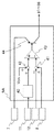
図1は、本実施の形態の電源回生コンバータの構成を示すブロック図である。以下にその構成について説明する。電源回生コンバータ1は、三相(R相、S相、T相)の交流電源を発生する三相交流電源3と、モータ5を可変速制御するインバータ装置4との間に配置される。ここで、電源回生コンバータ1は、交流電源端子51、52、53、54、55、56を備えている。交流電源端子51、52、53は、リアクトル2を介して三相交流電源3の各電源端子に接続され、交流電源端子54、55、56は、リアクトル2を介さずに三相交流電源3の各電源端子と接続する。また、電源回生コンバータ1の直流電源端子57、58はインバータ装置4内の直流母線に接続される。電源回生コンバータ1内には、直流電源端子57、58に接続される直流母線59、60が配置され、直流母線59、60間には、平滑コンデンサ71が接続される。平滑コンデンサ71の両端は、平滑コンデンサ71の両端電圧を検出するPN母線電圧検出部8に接続される。
電源回生コンバータ1内の直流母線59、60間には、回生トランジスタ81、82、83、84、85、86とダイオード91、92、93、94、95、96を備える回生部70が配設され、直流母線59、60間に、直列接続した回生トランジスタ81、82、回生トランジスタ83、84、および回生トランジスタ85、86の3組が並列に接続される。すなわち、直流母線59には、上アームを構成する回生トランジスタ81、83、85のコレクタ端子が接続され、直流母線60には、下アームを構成する回生トランジスタ82、84、86のエミッタ端子が接続される。そして、回生トランジスタ81のエミッタ端子と回生トランジスタ82のコレクタ端子とは、共通に交流電源端子51に接続される。同様に、回生トランジスタ83のエミッタ端子と回生トランジスタ84のコレクタ端子とは、交流電源端子52に接続され、回生トランジスタ85のエミッタ端子と回生トランジスタ86のコレクタ端子とは、交流電源端子53に接続される。なお、これらの回生トランジスタ81、82、83、84、85、86には、ダイオード91、92、93、94、95、96がそれぞれ並列に接続される。すなわち、ダイオードのアノード端子は回生トランジスタのエミッタ端子に接続され、ダイオードのカソード端子は回生トランジスタのコレクタ端子に接続される。
交流電源端子54、55、56は、三相交流電源3の三相間の電源電圧波形を検出する線間電圧検出部6に接続され、線間電圧検出部6の出力端は、歪成分が混在していない三相交流電源の線間電圧波形と定義する基本波形を生成する基本波形生成部10に接続される。基本波形生成部10の出力端子は、三相交流電源3の電圧位相に基づき回生トランジスタのオン/オフ制御を行うベース駆動信号を作成するベース駆動信号作成部7と、基本波形生成部10の出力に基づいて三相交流電源3の電圧値を算出する基準電圧検出部12とに接続される。ベース駆動信号作成部7、基準電圧検出部12、PN母線電圧検出部8の出力端は、三相交流電源3の電圧値と平滑コンデンサ71の両端電圧値に基づき、回生トランジスタのオン/オフ制御を行うベース駆動信号を出力するベース駆動信号出力部9に接続され、ベース駆動信号出力部9の出力端はそれぞれ回生トランジスタ81、82、83、84、85、86の対応するベース端子に接続される。
図1では、線間電圧検出部6の入力信号は、リアクトル2を介さない三相交流電源3の各相の電圧としたが、リアクトル2を介した三相交流電源3の各相の電圧としてもよい。Embodiment 1 FIG.
FIG. 1 is a block diagram showing the configuration of the power regeneration converter of the present embodiment. The configuration will be described below. The power regeneration converter 1 is disposed between a three-phase
A
The AC
In FIG. 1, the input signal of the line
次に、図1に示す電源回生コンバータの回生電流の流れについて説明する。まず、モータが減速することによって発生した誘導起電力による電流が平滑コンデンサ71の両端に流れ込むため、平滑コンデンサ71の電圧が上昇する。このため、電源から供給される三相電源電圧のうち最大電位を示す−相の電位が平滑コンデンサ71の+極よりも低くなり、三相の電源電圧のうち最小電位を示す−相の電位が平滑コンデンサ71の−極の電位よりも高くなる。したがって、供給される三相の電源電圧と平滑コンデンサ71との間に電位差が生ずるため、回生トランジスタをオンすることにより平滑コンデンサ71から電源へ回生電流が流れる。
Next, the flow of the regenerative current of the power regeneration converter shown in FIG. 1 will be described. First, since the current due to the induced electromotive force generated by the deceleration of the motor flows into both ends of the
このように、電源回生コンバータの平滑コンデンサ電圧と電源電圧の電圧差を利用し、リアクトルによる電流制限で電流を流すため、オンする回生トランジスタの位相を誤ると、電圧差が大きくなり、急激に大電流が流れて装置の停止や破損を招く恐れがある。そのため、電源位相の検出、回生トランジスタのオン/オフ制御が重要となる。 In this way, the difference between the smoothing capacitor voltage of the power regenerative converter and the power supply voltage is used to flow current with the current limiting by the reactor.Therefore, if the phase of the regenerative transistor that is turned on is incorrect, the voltage difference increases and suddenly increases. There is a risk of current flowing and causing the device to stop or break. Therefore, detection of the power supply phase and on / off control of the regenerative transistor are important.
以下、ベース駆動信号を用いた回生トランジスタのオン/オフ制御について説明する。
図2は、線間電圧検出部6からベース駆動信号作成部7までのブロック図である。図3は、基本波形生成部10の内部構成を示すブロック図である。図4は、線間電圧検出部6の出力波形と基本波形生成部10の出力波形を示す図である。図5は、1次ローパスフィルタI(s)および4次ローパスフィルタH(s)のボード線図を示す図である。Hereinafter, the on / off control of the regenerative transistor using the base drive signal will be described.
FIG. 2 is a block diagram from the
図2に示す通り、線間電圧検出部6は、三相交流電源3の三相それぞれの電圧波形VR、VS、VTを入力し、三相それぞれの線間電圧波形VR-S、VS-T、VT-Rを検出して、それらを出力する。基本波形生成部10は、線間電圧検出部6から出力された線間電圧波形VR-S、VS-T、VT-Rを入力し、線間電圧波形から基本波形V'R-S、V'S-T、V'T-Rを生成し、ベース駆動信号作成部7へ出力する。ベース駆動信号作成部7は、基本波形V'R-S、V'S-T、V'T-Rを用いて、回生トランジスタのオン/オフ制御に用いるベース駆動信号(この実施の形態では各回生トランジスタに対応した6つの信号)を作成する。
As shown in FIG. 2, the
次に、線間電圧検出部6について説明する。
線間電圧検出部6では、三相交流電源3よりR−S線間、S−T線間、T−R線間の線間電圧波形VR-S、VS-T、VT-Rを検出する。ここで、S−R線間電圧波形はR−S線間電圧波形の位相を180°進めたあるいは遅らせたものであり、T−S線間電圧波形はS−T線間電圧波形の位相を、R−T線間電圧波形はT−R線間電圧波形の位相を、それぞれ180°進めたあるいは遅らせたものである。よって、S−R線間、T−S線間、R−T線間の線間電圧波形は、線間電圧検出部6で検出するR−S線間、S−T線間、T−R線間の線間電圧波形から算出可能なので、上記3つの線間電圧波形VR-S、VS-T、VT-Rだけ検出すればよい。Next, the
The line
次に、基本波形生成部10について説明する。
三相交流電源3の歪成分の影響を受けることなく回生トランジスタのオン/オフ制御に用いるベース駆動信号を作成するために、基本波形生成部10を以下のように構成する。図3に示す通り、基本波形生成部10は、三相交流電源3の線間電圧波形VR-S、VS-T、VT-Rから歪成分を除去する高周波成分除去フィルタ21と、高周波成分除去フィルタ21の出力から三相交流電源3の線間電圧波形の基本周波数を算出する周波数算出部22と、高周波成分除去フィルタ21からの出力の補正を行う補正部23とを備える。図4に示す通り、高周波成分除去フィルタ21では、線間電圧波形に混在する歪成分を除去するが、除去後の波形は位相と振幅が変化してしまう。そこで補正部23において、周波数算出部22で算出された三相交流電源3の線間電圧波形の基本周波数を用いて、高周波成分除去フィルタ21で歪成分を除去することにより変化した位相と振幅を、歪成分を含まない場合の三相交流電源3の線間電圧波形の位相、振幅と同じにする補正を行う。よって、基本波形生成部10は、三相交流電源3の線間電圧波形VR-S、VS-T、VT-Rを入力し、歪成分を含まない三相交流電源3の線間電圧波形となる基本波形V'R-S、V'S-T、V'T-Rを出力する。Next, the basic
In order to generate a base drive signal used for on / off control of the regenerative transistor without being affected by the distortion component of the three-phase
次に、基本波形生成部10内の高周波数成分除去フィルタ21とその出力波形信号および補正部23について、詳細に説明する。
高周波成分除去フィルタ21は、FFTアナライザ機能を有するシステムで実現する他に、ローパスフィルタやバンドパスフィルタなど様々なフィルタでその機能を実現できるが、ここでは、2次ローパスフィルタを2段使用する4次ローパスフィルタの場合について説明する。このローパスフィルタにより、高周波である歪成分が除去され、その周波数は、歪成分がない三相交流電源3の周波数と同じなる。 Next, the high frequency
The high-frequency
まず、2次ローパスフィルタについて述べる。ωnを折点周波数、sをラプラス演算子とすると、2次ローパスフィルタの伝達関数G(s)は、(1)式のように表される。 First, a secondary low-pass filter will be described. When ωn is a break frequency and s is a Laplace operator, the transfer function G (s) of the second-order low-pass filter is expressed as in equation (1).

次に、2次ローパスフィルタを2段使用する4次ローパスフィルタの場合について考える。その場合の4次ローパスフィルタ伝達関数H(s)は、(3)式のようになる。 Next, consider the case of a quartic low-pass filter using two stages of secondary low-pass filters. In this case, the fourth-order low-pass filter transfer function H (s) is expressed by equation (3).
ここで、前記1次ローパスフィルタの伝達関数をI(s)とすると、I(s)通過後のゲイン減衰量g、位相遅れ量φは(4)式、(5)式のようになる。(ωは任意の周波数) Here, assuming that the transfer function of the first-order low-pass filter is I (s), the gain attenuation amount g and the phase delay amount φ after passing through I (s) are expressed by equations (4) and (5). (Ω is any frequency)
よって、高周波成分除去フィルタ21が2次ローパスフィルタを2段使用する4次ローパスフィルタH(s)の場合、(6)式、(7)式から、高周波成分除去フィルタ21のゲイン減衰量ghと位相遅れ量φhは、1次ローパスフィルタI(s)のゲイン減衰量gおよび位相遅れ量φのそれぞれ4倍となることが分かる。
また、図5に、1次ローパスフィルタI(s)と4次ローパスフィルタH(s)について、ゲイン対周波数の関係と位相対周波数の関係をそれぞれ直交座標上に表し一組としたボード線図を示す。これからも、4次ローパスフィルタH(s)のゲイン減衰量ghと位相遅れ量φhは、1次ローパスフィルタI(s)のゲイン減衰量gおよび位相遅れ量φのそれぞれ4倍となっていることが分かる。Therefore, when the high-frequency
FIG. 5 shows a Bode diagram in which the gain vs. frequency relationship and the phase vs. frequency relationship are represented on orthogonal coordinates for the first order low pass filter I (s) and the fourth order low pass filter H (s). Indicates. From now on, the gain attenuation amount gh and the phase delay amount φh of the fourth-order low-pass filter H (s) are each four times the gain attenuation amount g and the phase delay amount φ of the first-order low-pass filter I (s). I understand.
ここで、図4に示す通り、高周波成分除去フィルタ21の出力波形の周波数は、三相交流電源3の線間電圧波形の周波数と同じであるため、周波数算出部22において三相交流電源3の線間電圧波形の基本周波数を算出後、高周波成分除去フィルタ21の折点周波数ωnを基本周波数に変更する。そして、歪なしの三相交流電源3の線間電圧波形信号に対する、(3)式で表されるフィルタが出力する波形信号の位相遅れ量φは、(7)式から算出され、180度(=π)となる。また、線間電圧の位相検出には影響ないが、(3)式で表されるフィルタが出力する波形信号の振幅は、(6)式を用いて算出され、歪なしの三相交流電源3の線間電圧波形の振幅の1/4となる。従って、高周波除去フィルタ21の出力は、歪なしの三相交流電源3の線間電圧波形と比較して振幅1/4、位相が180度遅れた波形信号となる。
Here, as shown in FIG. 4, the frequency of the output waveform of the high-frequency
以下では、具体的な線間電圧波形を用いて、基本波形生成部10の動作を説明する。
三相交流電源3の、ある2相間の線間電圧波形をsin波形とすると、高周波成分除去フィルタ21へ入力前の信号である線間電圧波形y1(t)を(8)式で表すことができる。ここで、Aは振幅、tは時間である。なお、歪成分は一切混在していないものと考える。Below, operation | movement of the basic waveform production |
When the line voltage waveform between two phases of the three-phase
![]()
![]()
(9)式に示される高周波成分除去フィルタ21の出力波形信号y2(t)を、(8)式で表される三相交流電源3の線間電圧波形y1(t)と同じとするために、補正部23でその位相遅れ、振幅減衰分を補正する。この場合では、補正部23を、振幅を定数倍するフィルタで構成する。高周波成分除去フィルタ21の出力信号y2(t)を−4倍すれば、振幅が補正され、位相の遅れも補正される。これにより、前記2相間の線間電圧波形に対応する擬似的な基本波形を生成できる。
ここで、補正部23は、定数倍するフィルタに限らず、位相遅れ量およびゲイン減衰量を計算する機能を有し、様々な手法でこれらの機能を実現可能である。例えば、振幅の減衰はゼロで位相のみ操作することができるオールパスフィルタによって位相遅れを補正する方法が考えられる。In order to make the output waveform signal y2 (t) of the high-frequency
Here, the
以上のように、基本波形生成部10は、三相交流電源3の線間電圧波形VR-S、VS-T、VT-Rを入力し、高周波成分除去フィルタ21で三相交流電源3の線間電圧波形の歪成分を除去し、補正部23でその波形の振幅と位相を三相交流電源3の線間電圧波形の振幅と位相に等しくなるように補正して、歪成分を含まない三相交流電源3の線間電圧波形となる基本波形V'R-S、V'S-T、V'T-Rを生成し、これを出力する。
As described above, the basic
以下に、ベース駆動信号作成部7について説明する。
図6は、電源回生コンバータの回生動作中のタイムチャートであって、基本波形の電圧変化に対応する位相検出信号、回生トランジスタ、回生電流の時間的変化を示したものである。
図1に示すベース駆動信号作成部7は、基本波形生成部10で生成した基本波形V'R-S、V'S-T、V'T-Rを入力する。入力した基本波形V'R-S、V'S-T、V'T-Rの位相を180度進めるあるいは遅らせることで、基本波形V'S-R、V' T-S、V' R-Tを算出する。具体的には、基本波形V'R-S、V'S-T、V'T-Rに−1を掛ければよい。そして、各基本波形のゼロクロスを検出し、例えば図6に示すように、基本波形V'R-S、V'S-T、V'T-R、V'S-R、V' T-S、V' R-Tの振幅が正の位相間ではオン、負の位相間ではオフとなるように、各基本波形に対する位相検出信号を作成する。歪成分が混在しない三相交流電源の線間電圧波形は、ほぼsin波形のため基本波形もsin波形となり、位相検出信号のオンの位相区間の中央で基本波形の電位は最大となり、位相検出信号のオフの位相区間の中央で基本波形の電位は最小となる。よって、各位相検出信号より、基本波形の最大電位を示す相と最小電位を示す相を把握することができる。そして、回生トランジスタ81、83、85のうち、三相交流電源電圧の最大電位を示す相と接続した回生トランジスタをオンし、かつ、回生トランジスタ82、84、86のうち、三相交流電源電圧の最小電位を示す相と接続した回生トランジスタをオンし、その他の回生トランジスタはオフする、回生トランジスタ81〜86のオン/オフ制御を行うベース駆動信号を各回生トランジスタ毎に作成する。作成されたベース駆動信号はベース駆動信号出力部9へ出力される。Below, the base drive
FIG. 6 is a time chart during the regenerative operation of the power regenerative converter, and shows the temporal change of the phase detection signal, the regenerative transistor, and the regenerative current corresponding to the voltage change of the basic waveform.
The base
次に、回生動作について説明する。
図1に示すPN母線電圧検出部8では、直流母線電圧として平滑コンデンサ71の両端電圧を検出してベース駆動信号出力部9へ出力する。基準電圧検出部12では、移動平均フィルタなどを用いて、基本波形V'R-S、V'S-T、V'T-Rの絶対値を取った波形を基本波形の1周期(周波数の逆数)だけ積分して電圧振幅を検出する。この検出した電圧振幅値を歪成分が混在しない場合の三相交流電源3の線間電圧値として、ベース駆動信号出力部9へ出力する。図7は、ベース駆動信号出力部9の内部構成を示すブロック図である。ベース駆動信号出力部9では、基準電圧検出部12の出力信号およびPN母線電圧検出部8の出力信号を減算器41に入力させ、三相交流電源3の電圧値と直流母線電圧値との電圧差を算出する。そして、回生動作を開始するためのしきい値として予め設定した回生開始電圧値Vonと、減算器41の出力である三相交流電源3の電圧値と直流母線電圧値との電圧差と、を比較器43に入力して比較し、三相交流電源3の電圧値と直流母線電圧値との電圧差が回生開始電圧より高くなったとき、ベース駆動信号作成部7で作成した回生トランジスタのオン/オフ制御を行うベース駆動信号を回生トランジスタ81〜86に出力する回生動作を行う。Next, the regenerative operation will be described.
In the PN bus
図6の電源回生コンバータ1の回生動作中のタイムチャートで示す通り、基本波形V'R-Sの電位が最大の場合は、回生トランジスタ81と84をオンさせる。基本波形V'R-Tの電位が最大の場合は、回生トランジスタ81と86をオンさせる。基本波形V'S-Tの電位が最大の場合は、回生トランジスタ83と86をオンさせる。基本波形V'S-Rの電位が最大の場合は、回生トランジスタ82と83をオンさせる。基本波形V'T-Rの電位が最大の場合は、回生トランジスタ85と82をオンさせる。基本波形V'T-Sの電位が最大の場合は、回生トランジスタ84と85をオンさせる。
具体的には、時間t20〜t40で基本波形V'R-Sの電位が最大となるため、回生トランジスタ81と84をオンさせ、他の回生トランジスタはオフする。そうすれば、平滑コンデンサ71と三相交流電源のS−R相間は、リアクトルと電源インピーダンスを介して接続した状態となり、回生電流がR相からS相に流れる。同様に、時間t40〜t60では基本波形V'R-Tの電位が最大となるため、回生トランジスタ81と86をオンさせ、他の回生トランジスタをオフする。そうすれば、回生電流がR相からT相に流れる。As shown in the time chart during the regenerative operation of the power regeneration converter 1 in FIG. 6, when the potential of the basic waveform V′RS is maximum, the
Specifically, since the potential of the basic waveform V′RS becomes maximum at time t20 to t40, the
以上のように、三相交流電源3の線間電圧の基本波形を生成すれば、三相交流電源3に歪成分が混在した場合でも、歪成分の影響を受けず、三相交流電源の線間電圧波形の基本周波数が検出でき、基本波形から正確な三相交流電源の電圧位相を検出できる。また、ベース駆動信号作成において、この歪成分を含まない三相交流電源3の線間電圧波形となる基本波形を用いれば、各線間電圧のうち最大となる線間電圧の2つの相を接続させる回生トランジスタのみオンさせて、他の回生トランジスタをオフするような回生トランジスタオン/オフ制御を行うベース駆動信号を、三相交流電源の電圧位相に対して正確に作成することができる。従って、回生動作時に電源や回生コンバータに過電圧や過電流がかかることが無くなるので、これらが原因の電源や回生コンバータの破損によるシステム停止を防ぐことができる。
As described above, if the basic waveform of the line voltage of the three-phase
実施の形態2.
以下では、三相交流電源に歪成分が混在する場合にその歪成分を把握するため、実施の形態1に三相交流電源の歪成分を抽出し、歪成分の歪周波数、歪振幅、歪率を求める機能を付加した実施の形態について説明する。
図8は、本実施の形態の電源回生コンバータの構成を示すブロック図である。図9は、歪成分抽出部の内部構造を示す図である。図8に示す本実施の形態の電源回生コンバータ1Aは、実施の形態1の電源回生コンバータ1内の基本波形生成部10の後に三相交流電源3の線間電圧波形に混在する歪成分を抽出する歪成分抽出部11を設け、さらに、歪成分抽出部11の後に、抽出した歪成分の周波数を検出する歪成分周波数検出部24と、抽出した歪成分の電圧振幅を検出する歪電圧検出部25と、電源電圧歪の歪率(歪成分の電圧振幅/電源電圧の振幅)を算出する歪率算出部26を設けている。
In the following, in order to grasp the distortion component when the three-phase AC power supply is mixed, the distortion component of the three-phase AC power supply is extracted in the first embodiment, and the distortion frequency, distortion amplitude, and distortion rate of the distortion component are extracted. An embodiment to which a function for obtaining the above is added will be described.
FIG. 8 is a block diagram showing a configuration of the power regeneration converter according to the present embodiment. FIG. 9 is a diagram illustrating an internal structure of the distortion component extraction unit. The
図9に示す通り、歪成分抽出部11は、線間電圧検出部6からの出力で三相交流電源3の歪成分を含む線間電圧波形VR-S、VS-T、VT-Rと、基本波形生成部10からの出力で歪を含まず線間電圧波形と同じ周波数で振幅もほぼ等しい基本波形V'R-S、V'S-T、V'T-Rとを入力する。歪成分抽出部11では、減算器27で線間電圧波形VR-Sから基本波形V'R-Sが減算される。同様に、減算器28で線間電圧波形VS-Tから基本波形V'S-Tが、また減算器29で線間電圧波形VT-Rから基本波形V'T-Rがそれぞれ減算される。従って、減算器27、28、29により、三相交流電源3の線間電圧波形の歪成分VfR-S、VfS-T、VfT-Rが抽出され、それぞれ歪成分抽出部11から出力される。歪成分抽出部11から出力された歪成分VfR-S、VfS-T、VfT-Rは、歪成分周波数検出部24と歪電圧検出部25に入力される。
As shown in FIG. 9, the distortion
図8に示す通り、歪成分周波数検出部24は歪成分抽出部11から歪成分VfR-S、VfS-T、VfT-Rを入力して、歪成分の周波数を検出する。また、歪電圧検出部25は歪成分抽出部11から歪成分VfR-S、VfS-T、VfT-Rを入力して、移動平均フィルタなどを用いて、歪成分VfR-S、VfS-T、VfT-Rの絶対値を取った波形を各歪成分の1周期(周波数の逆数)だけ積分して歪成分の電圧振幅を検出する。さらに、歪率算出部26は基準電圧検出部12の出力(電源電圧)と歪電圧検出部25の出力(歪成分電圧)を入力して、それらを除算することにより歪率(歪成分の電圧振幅/電源電圧の振幅)を算出する。
As shown in FIG. 8, the distortion component
このように、歪成分抽出部11、歪成分周波数検出部24、歪電圧検出部25、歪率算出部26を設けることで、特別な測定器を使用することなく、三相交流電源3の線間電圧波形の歪成分の歪周波数、歪振幅、歪率を求めることができる。そして、三相交流電源3の線間電圧波形の歪成分の歪周波数、歪振幅、歪率を表示したり、これらの値が予め定めておいた範囲を逸脱した場合にアラーム等により警告を行うことで、電源状態を監視することができる。
Thus, by providing the distortion
また、このような表示、警告等により電源状態を監視することで、回生動作を行う前に電源状態を把握することができるので、電源に歪成分が混在し、それが回生動作に与える影響が大きい場合には、ベース駆動信号を出力しないなどして、回生動作を行わないようにすることができる。よって、回生動作により過電流が電源及び回生コンバータに流れることによる、これらの破壊を防ぐことができる。 Also, by monitoring the power supply status with such displays, warnings, etc., the power supply status can be ascertained before performing the regenerative operation.Therefore, distortion components are mixed in the power supply, which may affect the regenerative operation. If it is larger, the regenerative operation can be prevented from being performed by not outputting the base drive signal. Therefore, it is possible to prevent the destruction due to the overcurrent flowing to the power source and the regenerative converter by the regenerative operation.
実施の形態3.
以下では、三相交流電源に歪成分が混在する場合に、その歪成分の状態に応じて回生トランジスタのオン/オフ制御を行う機能を、実施の形態1に付加した実施の形態について説明する。
図10は、本実施の形態の電源回生コンバータの構成を示すブロック図である。図11は、本実施の形態におけるベース駆動信号出力部9Aの内部構成を示すブロック図である。図12は、電源回生コンバータ1Bが回生動作中のタイムチャートであって、歪成分が混在した三相交流電源3の線間電圧波形および基本波形に対応する回生トランジスタおよび回生電流の時間的変化を示したものである。
図10に示す本実施の形態の電源回生コンバータ1Bは、実施の形態1の電源回生コンバータの基本波形生成部10の後に三相交流電源3の三相間の電源電圧波形に混在する歪成分を抽出する歪成分抽出部11を設け、実施の形態1のベース駆動信号出力部9の代わりにベース駆動信号出力部9Aを設けている。ここで、歪成分抽出部11の出力はベース駆動信号出力部9Aに入力される。
In the following, an embodiment in which the function of performing on / off control of the regenerative transistor in accordance with the state of the distortion component when the distortion component is mixed in the three-phase AC power supply is described in the first embodiment.
FIG. 10 is a block diagram showing a configuration of the power regeneration converter according to the present embodiment. FIG. 11 is a block diagram showing an internal configuration of the base drive
The power regeneration converter 1B of the present embodiment shown in FIG. 10 extracts distortion components mixed in the power voltage waveform between the three phases of the three-phase
図11を用いてベース駆動信号出力部9A内の動作について説明する。
ベース駆動信号出力部9Aは、歪成分抽出部11の出力信号、ベース駆動信号作成部7の出力信号、基準電圧検出部12の出力信号、PN母線電圧検出部8の出力信号をそれぞれ入力し、6つの回生トランジスタのオン/オフ制御に用いるベース駆動信号を出力する。ベース駆動信号出力部9Aでは、三相交流電源3の電圧値と直流母線電圧値の差分値が、あるしきい値以上になったら、ベース駆動信号を出力し回生動作を開始するように構成する。The operation in the base drive
The base drive
基準電圧検出部12から出力される、歪成分が混在しない場合の三相交流電源3の線間電圧値と、PN母線電圧検出部8から出力される直流母線電圧値をベース駆動信号出力部9A内の減算器41に入力させ、歪成分が混在しない場合の三相交流電源3の線間電圧値と直流母線電圧値との電圧差を算出する。一方、三相交流電源3の線間電圧値が直流母線電圧より大きいときに回生動作を起こすことを防ぐため、歪成分が混在しない場合の回生開始電圧Vonと歪成分抽出部11を用いて、歪成分による電源電圧の低下上昇に対応した回生動作を開始するための電圧しきい値を生成する。まず、歪成分抽出部11の出力信号を歪成分補正部40に入力して補正を行い出力する。歪成分補正部40での補正は、歪成分の周期は維持し、周期以外(例えば振幅)の補正を行う。よって、歪成分補正部40は、歪成分抽出部11の出力信号に対して、例えば定数を掛けるものでも良い。そして、歪成分補正部40の出力信号と、回生開始電圧Vonとを加算器42に入力する。回生開始電圧Vonは回生動作を開始するためのしきい値として予め定めた定数なので、加算器42の出力信号は、歪成分により生じる電源の電圧低下、電圧上昇の周期に同期する。従って、加算器42の出力信号を、歪成分による電源電圧の低下上昇に対応した、回生動作を開始するための電圧しきい値とすることができる。
The base drive
加算器42の出力と減算器41の出力を比較器43に入力し、減算器41の出力信号と加算器42の出力信号を比較する。また、スイッチ44のコレクタ部にベース駆動信号作成部7の出力信号を入力し、比較器43の出力信号はスイッチ44のゲート部に接続する。スイッチ44のエミッタ部はそれぞれの回生トランジスタ81〜86のゲート部に接続する。ここで、減算器41の出力信号が加算器42の出力信号よりも大きい場合にスイッチ44をオンさせる。スイッチ44がオンすると、ベース駆動信号作成部7で作成されたベース駆動信号がベース駆動信号出力部9Aから出力される。出力されたベース駆動信号はそれぞれの回生トランジスタに入力され、回生トランジスタのオン/オフ制御を行う。
The output of the
以上のことから、三相交流電源3の歪成分を抽出して、その歪成分に対応して回生開始の電圧しきい値を変化させることで、回生トランジスタのオン/オフ制御を正確なタイミングで行うことができる。従って、従来では、その歪成分が回生動作に与える影響が大きい場合でも、安定した回生動作が実施できる。これにより、電源や回生コンバータに回生動作による過電圧、過電流がかかることがなくなるため、回生動作による電源や回生コンバータの破損を防ぐことができ、結果としてシステム停止を防ぐことができる。
From the above, the distortion component of the three-phase
この発明に係る電源回生コンバータは、電源電圧歪が混在する三相交流電源において安定した回生動作を得る場合に適している。 The power supply regenerative converter according to the present invention is suitable for obtaining a stable regenerative operation in a three-phase AC power supply in which power supply voltage distortion is mixed.
Claims (10)
前記ベース駆動信号出力部は、前記ベース駆動信号作成部の出力信号と前記基準電圧検出部からの出力信号と前記PN母線電圧検出部からの出力信号とを入力し、前記基準電圧検出部からの出力信号と前記PN母線電圧検出部からの出力信号との差分値に基づき、前記ベース駆動信号出力のオン/オフを行うことを特徴とする請求項1に記載の電源回生コンバータ。A reference voltage detection unit that detects a power supply voltage of the three-phase AC power supply from an output signal of the basic waveform generation unit, and a PN bus voltage detection unit that detects a terminal voltage of the smoothing capacitor,
The base drive signal output unit inputs an output signal of the base drive signal creation unit, an output signal from the reference voltage detection unit, and an output signal from the PN bus voltage detection unit, and outputs from the reference voltage detection unit The power regeneration converter according to claim 1, wherein the base drive signal output is turned on / off based on a difference value between an output signal and an output signal from the PN bus voltage detector.
前記歪成分抽出部の出力信号から電源電圧歪成分の電圧振幅を算出する歪電圧算出部と、前記歪成分抽出部の出力信号から電源電圧歪成分の周波数成分を算出する歪成分周波数算出部と、前記歪電圧算出部の出力信号と前記基準電圧検出部の出力信号とから電源電圧歪の歪率を算出する歪率算出部のうち、少なくとも1つをさらに備えたことを特徴とする電源回生コンバータ。A smoothing capacitor that accumulates the induced electromotive force generated by the three-phase induction motor, a regenerative transistor that switches the terminal voltage of the smoothing capacitor to perform a power regeneration operation on the three-phase AC power source, and a line voltage of the three-phase AC power source A basic waveform that generates a basic waveform that is defined as a line voltage waveform of the three-phase AC power supply that does not contain power supply voltage distortion components from an output signal of the line voltage detection unit A base drive signal generator for generating a base drive signal used for on / off control of a regenerative transistor based on an output signal of the basic waveform generator; a base drive signal output unit for outputting the base drive signal; A distortion component extraction unit that extracts a power supply voltage distortion component mixed in the three-phase AC power supply based on an output signal of the line voltage detection unit and an output signal of the basic waveform generation unit; Provided,
A distortion voltage calculation unit that calculates a voltage amplitude of a power supply voltage distortion component from an output signal of the distortion component extraction unit; and a distortion component frequency calculation unit that calculates a frequency component of a power supply voltage distortion component from the output signal of the distortion component extraction unit; A power regeneration system further comprising at least one of a distortion rate calculation unit for calculating a distortion rate of a power supply voltage distortion from an output signal of the distortion voltage calculation unit and an output signal of the reference voltage detection unit. converter.
前記ベース駆動信号出力部は、前記歪成分抽出部の出力信号について補正を行う歪成分補正部と、電源電圧歪が混在しない場合の回生動作を開始するためのしきい値となる回生開始電圧と前記歪成分補正部の出力信号とを加算する加算器と、前記PN母線電圧検出部の出力信号と前記基準電圧検出部の出力信号とを入力し減算を行う減算器と、前記加算器の出力信号と前記減算器の出力信号を入力し比較を行う比較器と、前記比較器の出力信号に基づき、前記ベース駆動信号作成部の出力信号を回生トランジスタへ出力するスイッチ部を備えたことを特徴とする電源回生コンバータ。A smoothing capacitor that accumulates the induced electromotive force generated by the three-phase induction motor, a regenerative transistor that switches the terminal voltage of the smoothing capacitor to perform a power regeneration operation on the three-phase AC power source, and a line voltage of the three-phase AC power source A basic waveform that generates a basic waveform that is defined as a line voltage waveform of the three-phase AC power supply that does not contain power supply voltage distortion components from an output signal of the line voltage detection unit A base drive signal generator for generating a base drive signal used for on / off control of a regenerative transistor based on an output signal of the basic waveform generator; a base drive signal output unit for outputting the base drive signal; A distortion component extraction unit that extracts a power supply voltage distortion component mixed in the three-phase AC power supply based on an output signal of the line voltage detection unit and an output signal of the basic waveform generation unit; Comprising a reference voltage detection unit from serial output signal of the basic waveform generating unit for detecting a power supply voltage of the three-phase AC power supply, and a PN bus voltage detecting unit for detecting a terminal voltage of the smoothing capacitor,
The base drive signal output unit includes a distortion component correction unit that corrects the output signal of the distortion component extraction unit, and a regeneration start voltage that serves as a threshold value for starting a regeneration operation when power supply voltage distortion is not mixed. An adder for adding the output signal of the distortion component correction unit, a subtractor for inputting and subtracting the output signal of the PN bus voltage detection unit and the output signal of the reference voltage detection unit, and the output of the adder A comparator for inputting and comparing the signal and the output signal of the subtractor; and a switch unit for outputting the output signal of the base drive signal generating unit to the regenerative transistor based on the output signal of the comparator. And power regeneration converter.
Applications Claiming Priority (1)
| Application Number | Priority Date | Filing Date | Title |
|---|---|---|---|
| PCT/JP2007/057860 WO2008129623A1 (en) | 2007-04-10 | 2007-04-10 | Power supply regenerative converter |
Publications (2)
| Publication Number | Publication Date |
|---|---|
| JPWO2008129623A1 JPWO2008129623A1 (en) | 2010-07-22 |
| JP4924711B2 true JP4924711B2 (en) | 2012-04-25 |
Family
ID=39875171
Family Applications (1)
| Application Number | Title | Priority Date | Filing Date |
|---|---|---|---|
| JP2009510661A Active JP4924711B2 (en) | 2007-04-10 | 2007-04-10 | Power regeneration converter |
Country Status (6)
| Country | Link |
|---|---|
| US (1) | US8188701B2 (en) |
| JP (1) | JP4924711B2 (en) |
| CN (1) | CN101652920B (en) |
| DE (1) | DE112007003407T5 (en) |
| TW (1) | TW200841564A (en) |
| WO (1) | WO2008129623A1 (en) |
Families Citing this family (13)
| Publication number | Priority date | Publication date | Assignee | Title |
|---|---|---|---|---|
| CN102349030B (en) * | 2009-01-26 | 2014-10-15 | 吉尼瓦洁净技术公司 | Energy usage monitoring with remote display and automatic detection of appliance including graphical user interface |
| US8674544B2 (en) * | 2009-01-26 | 2014-03-18 | Geneva Cleantech, Inc. | Methods and apparatus for power factor correction and reduction of distortion in and noise in a power supply delivery network |
| JP5464981B2 (en) * | 2009-11-18 | 2014-04-09 | 日本リライアンス株式会社 | AC / DC converter |
| JP5452259B2 (en) * | 2010-01-29 | 2014-03-26 | 三菱電機株式会社 | Power regeneration converter |
| JP5653429B2 (en) * | 2010-06-23 | 2015-01-14 | 住友重機械工業株式会社 | Injection molding machine and power regeneration converter |
| JP5257533B2 (en) * | 2011-09-26 | 2013-08-07 | ダイキン工業株式会社 | Power converter |
| CN103036529B (en) | 2011-09-29 | 2017-07-07 | 株式会社大亨 | Signal processing apparatus, wave filter, control circuit, inverter and converter system |
| DK2575252T3 (en) | 2011-09-29 | 2018-10-08 | Daihen Corp | Signal processor, filter, power converter for power converter circuit, connection inverter system and PWM inverter system |
| JP5664588B2 (en) * | 2012-04-20 | 2015-02-04 | 株式会社安川電機 | Power regeneration device and power conversion device |
| JP6453108B2 (en) * | 2015-02-25 | 2019-01-16 | 日立ジョンソンコントロールズ空調株式会社 | Power conversion device, active filter, and motor drive device |
| WO2017033320A1 (en) * | 2015-08-26 | 2017-03-02 | 三菱電機株式会社 | Power supply regenerative converter and motor control device |
| JP6503413B2 (en) * | 2017-05-31 | 2019-04-17 | 本田技研工業株式会社 | DC / DC converter and electrical equipment |
| JP6871835B2 (en) * | 2017-09-27 | 2021-05-12 | 三菱重工サーマルシステムズ株式会社 | Control devices, control methods and programs |
Citations (3)
| Publication number | Priority date | Publication date | Assignee | Title |
|---|---|---|---|---|
| JPH07107747A (en) * | 1993-09-30 | 1995-04-21 | Meidensha Corp | Converter device |
| JP2004180427A (en) * | 2002-11-27 | 2004-06-24 | Mitsubishi Electric Corp | Regenerative power supply converter |
| WO2007122701A1 (en) * | 2006-04-19 | 2007-11-01 | Mitsubishi Denki Kabushiki Kaisha | Converter apparatus |
Family Cites Families (9)
| Publication number | Priority date | Publication date | Assignee | Title |
|---|---|---|---|---|
| JPH05304779A (en) | 1991-04-04 | 1993-11-16 | Mitsubishi Electric Corp | Regenerative power control device |
| EP0657991B1 (en) * | 1993-12-09 | 1997-11-05 | Hitachi, Ltd. | Signal detecting circuit for digital controller |
| JP3706960B2 (en) | 1993-12-09 | 2005-10-19 | 株式会社日立製作所 | Signal detection circuit for digital controller |
| JP3261010B2 (en) | 1995-05-31 | 2002-02-25 | オークマ株式会社 | Power converter |
| US5790396A (en) * | 1995-12-19 | 1998-08-04 | Kabushiki Kaisha Toshiba | Neutral point clamped (NPC) inverter control system |
| JP3323759B2 (en) | 1996-10-23 | 2002-09-09 | 株式会社日立製作所 | Pulse width modulation converter device |
| JP3403056B2 (en) * | 1998-03-12 | 2003-05-06 | 株式会社東芝 | Converter control device |
| JP2000059995A (en) | 1998-08-05 | 2000-02-25 | Nichicon Corp | Compensating apparatus of higher-harmonic reactive power for power system |
| JP2000253686A (en) | 1999-03-03 | 2000-09-14 | Okuma Corp | Power regenerating circuit |
-
2007
- 2007-04-10 US US12/524,316 patent/US8188701B2/en active Active
- 2007-04-10 WO PCT/JP2007/057860 patent/WO2008129623A1/en active Application Filing
- 2007-04-10 JP JP2009510661A patent/JP4924711B2/en active Active
- 2007-04-10 CN CN2007800525366A patent/CN101652920B/en active Active
- 2007-04-10 DE DE112007003407T patent/DE112007003407T5/en not_active Withdrawn
- 2007-04-17 TW TW096113428A patent/TW200841564A/en unknown
Patent Citations (3)
| Publication number | Priority date | Publication date | Assignee | Title |
|---|---|---|---|---|
| JPH07107747A (en) * | 1993-09-30 | 1995-04-21 | Meidensha Corp | Converter device |
| JP2004180427A (en) * | 2002-11-27 | 2004-06-24 | Mitsubishi Electric Corp | Regenerative power supply converter |
| WO2007122701A1 (en) * | 2006-04-19 | 2007-11-01 | Mitsubishi Denki Kabushiki Kaisha | Converter apparatus |
Also Published As
| Publication number | Publication date |
|---|---|
| JPWO2008129623A1 (en) | 2010-07-22 |
| TW200841564A (en) | 2008-10-16 |
| TWI342100B (en) | 2011-05-11 |
| DE112007003407T5 (en) | 2010-01-07 |
| CN101652920B (en) | 2012-09-26 |
| CN101652920A (en) | 2010-02-17 |
| US8188701B2 (en) | 2012-05-29 |
| WO2008129623A1 (en) | 2008-10-30 |
| US20100052598A1 (en) | 2010-03-04 |
Similar Documents
| Publication | Publication Date | Title |
|---|---|---|
| JP4924711B2 (en) | Power regeneration converter | |
| EP2775597B1 (en) | Method and apparatus for ripple and phase loss detection | |
| US8947838B2 (en) | Overcurrent fault detection device for electrical drive control system | |
| JP2017530672A (en) | Grid tie inverter safety detection device and method | |
| US20130279213A1 (en) | Power regeneration apparatus and power conversion apparatus | |
| EP3116117B1 (en) | Inverter testing apparatus | |
| KR101661379B1 (en) | Apparatus for estimating capacitance of dc-link capacitor in inverter | |
| EP2933893A1 (en) | Active filter control device | |
| KR101929519B1 (en) | Three level neutral point clamped inverter system having imbalance capacitor voltages and its control method | |
| JP2010193704A (en) | Robust ac chassis fault detection using pwm sideband harmonics | |
| JP6103155B2 (en) | Power converter, power generation system, and current control method | |
| Freire et al. | A voltage-based approach for open-circuit fault diagnosis in voltage-fed SVM motor drives without extra hardware | |
| JP5300349B2 (en) | Motor control device and motor ground fault detection method | |
| KR101814224B1 (en) | Device for operating synchronous motors and associated method | |
| JP2018057157A (en) | Electric power conversion system | |
| JP6889026B2 (en) | Power converter | |
| JP2015192582A (en) | Current-sensor failure detection apparatus | |
| JP2009115634A (en) | Power supply system and current measurement method of power supply system | |
| JP6361398B2 (en) | Control device for power conversion device for grid connection, and power conversion device for grid connection | |
| JP5452259B2 (en) | Power regeneration converter | |
| JP2019161876A (en) | Insulation degradation detector for electric motor | |
| JP2018009875A (en) | Ground fault detection device | |
| JP4176709B2 (en) | AC / DC bidirectional converter | |
| JP2014039444A (en) | System interconnection inverter device | |
| CN107918058B (en) | Filter inductor detection method and device |
Legal Events
| Date | Code | Title | Description |
|---|---|---|---|
| A131 | Notification of reasons for refusal |
Free format text: JAPANESE INTERMEDIATE CODE: A131 Effective date: 20110531 |
|
| A521 | Request for written amendment filed |
Free format text: JAPANESE INTERMEDIATE CODE: A523 Effective date: 20110711 |
|
| TRDD | Decision of grant or rejection written | ||
| A01 | Written decision to grant a patent or to grant a registration (utility model) |
Free format text: JAPANESE INTERMEDIATE CODE: A01 Effective date: 20120110 |
|
| A01 | Written decision to grant a patent or to grant a registration (utility model) |
Free format text: JAPANESE INTERMEDIATE CODE: A01 |
|
| A61 | First payment of annual fees (during grant procedure) |
Free format text: JAPANESE INTERMEDIATE CODE: A61 Effective date: 20120123 |
|
| FPAY | Renewal fee payment (event date is renewal date of database) |
Free format text: PAYMENT UNTIL: 20150217 Year of fee payment: 3 |
|
| R151 | Written notification of patent or utility model registration |
Ref document number: 4924711 Country of ref document: JP Free format text: JAPANESE INTERMEDIATE CODE: R151 |
|
| FPAY | Renewal fee payment (event date is renewal date of database) |
Free format text: PAYMENT UNTIL: 20150217 Year of fee payment: 3 |
|
| R250 | Receipt of annual fees |
Free format text: JAPANESE INTERMEDIATE CODE: R250 |
|
| R250 | Receipt of annual fees |
Free format text: JAPANESE INTERMEDIATE CODE: R250 |
|
| R250 | Receipt of annual fees |
Free format text: JAPANESE INTERMEDIATE CODE: R250 |
|
| R250 | Receipt of annual fees |
Free format text: JAPANESE INTERMEDIATE CODE: R250 |
|
| R250 | Receipt of annual fees |
Free format text: JAPANESE INTERMEDIATE CODE: R250 |
|
| R250 | Receipt of annual fees |
Free format text: JAPANESE INTERMEDIATE CODE: R250 |
|
| R250 | Receipt of annual fees |
Free format text: JAPANESE INTERMEDIATE CODE: R250 |
|
| R250 | Receipt of annual fees |
Free format text: JAPANESE INTERMEDIATE CODE: R250 |
|
| R250 | Receipt of annual fees |
Free format text: JAPANESE INTERMEDIATE CODE: R250 |