JP6103155B2 - Power converter, power generation system, and current control method - Google Patents
Power converter, power generation system, and current control method Download PDFInfo
- Publication number
- JP6103155B2 JP6103155B2 JP2016551383A JP2016551383A JP6103155B2 JP 6103155 B2 JP6103155 B2 JP 6103155B2 JP 2016551383 A JP2016551383 A JP 2016551383A JP 2016551383 A JP2016551383 A JP 2016551383A JP 6103155 B2 JP6103155 B2 JP 6103155B2
- Authority
- JP
- Japan
- Prior art keywords
- unit
- voltage amplitude
- output current
- vibration component
- power
- Prior art date
- Legal status (The legal status is an assumption and is not a legal conclusion. Google has not performed a legal analysis and makes no representation as to the accuracy of the status listed.)
- Active
Links
Images


Classifications
-
- H—ELECTRICITY
- H02—GENERATION; CONVERSION OR DISTRIBUTION OF ELECTRIC POWER
- H02J—CIRCUIT ARRANGEMENTS OR SYSTEMS FOR SUPPLYING OR DISTRIBUTING ELECTRIC POWER; SYSTEMS FOR STORING ELECTRIC ENERGY
- H02J3/00—Circuit arrangements for ac mains or ac distribution networks
- H02J3/24—Arrangements for preventing or reducing oscillations of power in networks
-
- G—PHYSICS
- G01—MEASURING; TESTING
- G01R—MEASURING ELECTRIC VARIABLES; MEASURING MAGNETIC VARIABLES
- G01R19/00—Arrangements for measuring currents or voltages or for indicating presence or sign thereof
- G01R19/04—Measuring peak values or amplitude or envelope of ac or of pulses
-
- H—ELECTRICITY
- H02—GENERATION; CONVERSION OR DISTRIBUTION OF ELECTRIC POWER
- H02M—APPARATUS FOR CONVERSION BETWEEN AC AND AC, BETWEEN AC AND DC, OR BETWEEN DC AND DC, AND FOR USE WITH MAINS OR SIMILAR POWER SUPPLY SYSTEMS; CONVERSION OF DC OR AC INPUT POWER INTO SURGE OUTPUT POWER; CONTROL OR REGULATION THEREOF
- H02M1/00—Details of apparatus for conversion
- H02M1/14—Arrangements for reducing ripples from dc input or output
-
- H—ELECTRICITY
- H02—GENERATION; CONVERSION OR DISTRIBUTION OF ELECTRIC POWER
- H02M—APPARATUS FOR CONVERSION BETWEEN AC AND AC, BETWEEN AC AND DC, OR BETWEEN DC AND DC, AND FOR USE WITH MAINS OR SIMILAR POWER SUPPLY SYSTEMS; CONVERSION OF DC OR AC INPUT POWER INTO SURGE OUTPUT POWER; CONTROL OR REGULATION THEREOF
- H02M7/00—Conversion of ac power input into dc power output; Conversion of dc power input into ac power output
- H02M7/42—Conversion of dc power input into ac power output without possibility of reversal
- H02M7/44—Conversion of dc power input into ac power output without possibility of reversal by static converters
- H02M7/48—Conversion of dc power input into ac power output without possibility of reversal by static converters using discharge tubes with control electrode or semiconductor devices with control electrode
- H02M7/53—Conversion of dc power input into ac power output without possibility of reversal by static converters using discharge tubes with control electrode or semiconductor devices with control electrode using devices of a triode or transistor type requiring continuous application of a control signal
- H02M7/537—Conversion of dc power input into ac power output without possibility of reversal by static converters using discharge tubes with control electrode or semiconductor devices with control electrode using devices of a triode or transistor type requiring continuous application of a control signal using semiconductor devices only, e.g. single switched pulse inverters
- H02M7/5387—Conversion of dc power input into ac power output without possibility of reversal by static converters using discharge tubes with control electrode or semiconductor devices with control electrode using devices of a triode or transistor type requiring continuous application of a control signal using semiconductor devices only, e.g. single switched pulse inverters in a bridge configuration
- H02M7/53871—Conversion of dc power input into ac power output without possibility of reversal by static converters using discharge tubes with control electrode or semiconductor devices with control electrode using devices of a triode or transistor type requiring continuous application of a control signal using semiconductor devices only, e.g. single switched pulse inverters in a bridge configuration with automatic control of output voltage or current
- H02M7/53875—Conversion of dc power input into ac power output without possibility of reversal by static converters using discharge tubes with control electrode or semiconductor devices with control electrode using devices of a triode or transistor type requiring continuous application of a control signal using semiconductor devices only, e.g. single switched pulse inverters in a bridge configuration with automatic control of output voltage or current with analogue control of three-phase output
-
- H—ELECTRICITY
- H02—GENERATION; CONVERSION OR DISTRIBUTION OF ELECTRIC POWER
- H02J—CIRCUIT ARRANGEMENTS OR SYSTEMS FOR SUPPLYING OR DISTRIBUTING ELECTRIC POWER; SYSTEMS FOR STORING ELECTRIC ENERGY
- H02J3/00—Circuit arrangements for ac mains or ac distribution networks
- H02J3/38—Arrangements for parallely feeding a single network by two or more generators, converters or transformers
-
- H—ELECTRICITY
- H02—GENERATION; CONVERSION OR DISTRIBUTION OF ELECTRIC POWER
- H02M—APPARATUS FOR CONVERSION BETWEEN AC AND AC, BETWEEN AC AND DC, OR BETWEEN DC AND DC, AND FOR USE WITH MAINS OR SIMILAR POWER SUPPLY SYSTEMS; CONVERSION OF DC OR AC INPUT POWER INTO SURGE OUTPUT POWER; CONTROL OR REGULATION THEREOF
- H02M1/00—Details of apparatus for conversion
- H02M1/0003—Details of control, feedback or regulation circuits
- H02M1/0009—Devices or circuits for detecting current in a converter
-
- H—ELECTRICITY
- H02—GENERATION; CONVERSION OR DISTRIBUTION OF ELECTRIC POWER
- H02M—APPARATUS FOR CONVERSION BETWEEN AC AND AC, BETWEEN AC AND DC, OR BETWEEN DC AND DC, AND FOR USE WITH MAINS OR SIMILAR POWER SUPPLY SYSTEMS; CONVERSION OF DC OR AC INPUT POWER INTO SURGE OUTPUT POWER; CONTROL OR REGULATION THEREOF
- H02M1/00—Details of apparatus for conversion
- H02M1/08—Circuits specially adapted for the generation of control voltages for semiconductor devices incorporated in static converters
Description
開示の実施形態は、電力変換装置、発電システムおよび電流制御方法に関する。 Embodiments disclosed herein relate to a power conversion device, a power generation system, and a current control method.
近年、太陽電池や風力発電機などの発電装置の導入が拡大している。かかる発電装置と電力系統との間には、系統連系用電力変換装置が設置される。かかる電力変換装置は、発電装置の発電電力を電力系統の周波数に合わせた交流電力に変換し電力系統へ出力する。 In recent years, the introduction of power generation devices such as solar cells and wind power generators has expanded. A grid interconnection power converter is installed between the power generator and the power grid. Such a power conversion device converts the power generated by the power generation device into AC power that matches the frequency of the power system and outputs the AC power to the power system.
発電装置が電力系統に広域・大量に連系された場合、電力系統の擾乱により一斉に解列すると電力品質に大きな影響を与えることが懸念される。そのため、電力変換装置において、電力系統の瞬時電圧低下時などの系統電圧異常時に不要解列を防止し運転を継続する機能を備えることが要求されてきている。 When power generators are connected to a power system in a wide area and in large quantities, there is a concern that power quality will be greatly affected if they are disconnected all at once due to power system disturbance. For this reason, power converters have been required to have a function of preventing unnecessary disconnection and continuing operation when a system voltage abnormality such as an instantaneous voltage drop of the power system.
系統電圧異常は、例えば、線間短絡などによって生じる。線間短絡が発生すると、系統電圧がアンバランスになる。電力変換装置は、系統電圧がアンバランスになると、電圧位相を喪失するおそれがある。 The system voltage abnormality is caused by, for example, a line short circuit. When a line short circuit occurs, the system voltage becomes unbalanced. When the system voltage becomes unbalanced, the power conversion device may lose the voltage phase.
そこで、例えば、電力系統の電圧低下異常が発生する前の正常時の位相情報を保持し、電力系統の電圧低下異常が生じたと判定した場合に、保持された位相情報に基づいて出力電流を制御する電力変換装置が提案されている(例えば、特許文献1参照)。 Therefore, for example, when normal phase information before occurrence of power system voltage drop abnormality is held and it is determined that power system voltage drop abnormality has occurred, output current is controlled based on the held phase information The power converter device which performs is proposed (for example, refer to patent documents 1).
実施形態の一態様は、系統電圧異常時に出力電流を精度よく制御することができる電力変換装置、発電システムおよび電流制御方法を提供することを目的とする。 An object of one embodiment is to provide a power conversion device, a power generation system, and a current control method capable of accurately controlling an output current when a system voltage is abnormal.
実施形態の一態様に係る電力変換装置は、電力変換部と、電圧振幅取得部と、制御部とを備える。前記電力変換部は、電力系統に接続される。前記電圧振幅取得部は、前記電力系統の電圧振幅を取得する。前記制御部は、前記電圧振幅取得部により取得された前記電圧振幅の振動成分に基づいて、前記電力変換部から前記電力系統への出力電流を制御する。 A power conversion device according to an aspect of an embodiment includes a power conversion unit, a voltage amplitude acquisition unit, and a control unit. The power conversion unit is connected to a power system. The voltage amplitude acquisition unit acquires a voltage amplitude of the power system. The control unit controls an output current from the power conversion unit to the power system based on a vibration component of the voltage amplitude acquired by the voltage amplitude acquisition unit.
実施形態の一態様によれば、系統電圧異常時に出力電流を精度よく制御することができる電力変換装置、発電システムおよび電流制御方法を提供することができる。 According to one aspect of the embodiment, it is possible to provide a power conversion device, a power generation system, and a current control method that can accurately control an output current when a system voltage is abnormal.
以下、添付図面を参照して、本願の開示する電力変換装置、発電システムおよび電流制御方法の実施形態を詳細に説明する。なお、以下に示す実施形態によりこの発明が限定されるものではない。 Hereinafter, embodiments of a power conversion device, a power generation system, and a current control method disclosed in the present application will be described in detail with reference to the accompanying drawings. In addition, this invention is not limited by embodiment shown below.
[1.発電システム]
図1は、実施形態に係る発電システムの構成例を示す図である。図1に示す発電システム100は、電力変換装置1および発電装置2を備える。電力変換装置1は、発電装置2で発電された直流電力を電力系統3の電圧および周波数に合わせた交流電力へ変換して電力系統3へ出力する。なお、発電装置2は、例えば、太陽電池、直流発電機、燃料電池などである。[1. Power generation system]
FIG. 1 is a diagram illustrating a configuration example of a power generation system according to an embodiment. A
電力変換装置1は、電力変換部10と、電圧検出部14と、電流検出部15と、位相・振幅検出部20と、制御部23とを備える。電力変換部10は、制御部23による制御に基づき、発電装置2から供給される直流電力を電力系統3の電圧および周波数に合わせた交流電力へ変換して電力系統3へ出力する。
The
電圧検出部14は、例えば、電力系統3の交流電圧の瞬時値を繰り返し検出する。電流検出部15は、例えば、電力変換部10から電力系統3への出力電流の瞬時値(以下、検出電流と記載する場合がある)を繰り返し検出する。
For example, the
位相・振幅検出部20(電圧振幅取得部の一例)は、例えば、電圧検出部14の電圧検出結果に基づいて、電力系統3の電圧位相θおよび電力系統3の電圧振幅Ugを取得する。なお、位相・振幅検出部20は、外部から電圧位相θおよび電圧振幅Ugを取得することもできる。
The phase / amplitude detection unit 20 (an example of a voltage amplitude acquisition unit) acquires, for example, the voltage phase θ of the
制御部23は、位相・振幅検出部20により取得された電圧振幅Ugの振動成分に基づいて電力変換部10から電力系統3への出力電流を制御する。電力系統3に線間短絡などの電圧異常(以下、系統電圧異常と記載する場合がある)が発生した場合であっても、出力電流を精度よく制御することができる。なお、系統電圧異常には、例えば、電力系統3の電圧が過大な状態も含まれる。
The
制御部23は、例えば、電圧位相θに応じて検出電流の座標変換を行い、かかる座標変換後の検出電流が出力電流指令と一致するように電力変換部10を制御することができる。この場合、制御部23は、出力電流指令を電圧振幅Ugの振動成分に応じて座標変換後の検出電流や出力電流指令を補正する。これにより、出力電流を精度よく制御することができる。
For example, the
[2.電力変換装置]
図2は、図1に示す電力変換装置1の構成の一例を示す図である。図2に示すように、電力変換装置1は、電力変換部10と、電圧検出部11、13、14と、電流検出部12、15と、フィルタ18と、入力端子Tp、Tnと、出力端子Tr、Ts、Ttと、位相・振幅検出部20と、dq演算部21と、電圧異常検出部22と、制御部23とを備える。[2. Power conversion device]
FIG. 2 is a diagram illustrating an example of the configuration of the
電力変換部10は、昇圧回路16と、インバータ回路17とを備える。昇圧回路16は、例えば、昇圧チョッパ回路やDC−DCコンバータであり、また、インバータ回路17は、例えば、3相インバータである。なお、電力変換部10は、昇圧回路16に代えて、供給電圧Vinを所定の電圧に昇圧する降圧回路を備えることもでき、また、電力変換部10は、昇圧回路16を設けない構成であってもよい。
The
図3は、電力変換部10の構成の一例を示す図である。図3に示す昇圧回路16は、スイッチング素子Q7を有するチョッパ回路である。かかるスイッチング素子Q7は、制御部23から出力される駆動信号S7によってON/OFFが制御され、これにより、昇圧回路16において供給電圧Vinが所定の電圧に昇圧される。なお、図示しないが昇圧回路16は、例えば、制御部23から出力される駆動信号S7を増幅してスイッチング素子Q7のベースへ入力する増幅回路を有する。
FIG. 3 is a diagram illustrating an example of the configuration of the
また、図3に示すインバータ回路17は、3相ブリッジ接続された複数のスイッチング素子Q1〜Q6を含む3相インバータである。かかるスイッチング素子Q1〜Q6は、制御部23から出力される駆動信号S1〜S6によりON/OFFが制御され、これにより、インバータ回路17において、直流電圧が3相交流電圧へ変換される。なお、図示しないがインバータ回路17は、例えば、制御部23から出力される駆動信号S1〜S6を増幅してスイッチング素子Q1〜Q6のベースへ入力する増幅回路を有する。
Further, the
図2に戻って電力変換装置1の説明を続ける。電圧検出部11は、発電装置2から電力変換部10へ供給される電圧の瞬時値を供給電圧Vinとして検出する。また、電圧検出部13は、昇圧回路16から出力される昇圧後の直流電圧の瞬時値(以下、直流母線電圧Vpnと記載する)を検出する。電流検出部12は、例えば、発電装置2から電力変換部10へ供給される直流電流の瞬時値(以下、供給電流Iinと記載する)を検出する。
Returning to FIG. 2, the description of the
電圧検出部14は、例えば、電力系統3のR相とS相との間の瞬時電圧Vrs(以下、相間電圧Vrsと記載する)と、電力系統3のS相とT相との間の瞬時電圧Vst(以下、相間電圧Vstと記載する)とを検出する。
For example, the
電流検出部15は、例えば、電力変換部10から電力系統3のR相、S相およびT相へ出力される交流電流の瞬時値(以下、出力電流Ir、Is、Itと記載する)を検出する。フィルタ18は、例えば、LCフィルタであり、インバータ回路17を構成するスイッチング素子Q1〜Q6のスイッチングに起因するスイッチングノイズを除去する。
The
位相・振幅検出部20は、電圧検出部14によって検出された相間電圧Vrs、Vstに基づいて、電力系統3の電圧位相θおよび電力系統3の電圧振幅Ugを取得する。例えば、位相・振幅検出部20は、下記式(1)、(2)の演算により、相間電圧Vrs、Vstを2軸のαβ成分の交流電圧Vα、Vβへ変換する。
Vα=(2Vrs+Vst)÷2 ・・・(1)
Vβ=√3×Vst÷2 ・・・(2)The phase /
Vα = (2Vrs + Vst) ÷ 2 (1)
Vβ = √3 × Vst ÷ 2 (2)
位相・振幅検出部20は、交流電圧Vα、Vβに基づき、例えば、下記式(3)、(4)の演算により、電圧位相θおよび電圧振幅Ugを求める。
θ=tan-1(Vα,Vβ) ・・・(3)
Ug=√(Vα2+Vβ2) ・・・(4)The phase /
θ = tan −1 (Vα, Vβ) (3)
Ug = √ (Vα 2 + Vβ 2 ) (4)
なお、電圧検出部14は、例えば、電力系統3のR相、S相およびT相の瞬時電圧(以下、相電圧Vr、Vs、Vtと記載する)を検出することができる。この場合、位相・振幅検出部20は、例えば、相電圧Vr、Vs、Vtを3相2相変換により交流電圧Vα、Vβへ変換することができる。
The
また、位相・振幅検出部20は、電圧位相θおよび電圧振幅Ugを検出して取得するものであるが、位相・振幅検出部20に代えて、電圧位相θを検出して取得する位相検出部と、電圧振幅Ugを検出して取得する振幅検出部(電圧振幅取得部の一例)とをそれぞれ設ける構成であってもよい。なお、位相・振幅検出部20は、電圧位相θや電圧振幅Ugは、例えば、電力系統の管理装置から取得することもできる。
The phase /
dq演算部21は、出力電流Ir、Is、Itをα軸電流Iαおよびβ軸電流Iβへ変換し、α軸電流Iαおよびβ軸電流Iβをq軸電流Iqおよびd軸電流Idへ変換する。dq演算部21は、例えば、下記式(5)、(6)を用いて出力電流Ir、Is、Itをα軸電流Iαおよびβ軸電流Iβへ変換し、下記式(7)、(8)の演算によりα軸電流Iαおよびβ軸電流Iβをq軸電流Iqおよびd軸電流Idへ変換することができる。なお、電流検出部15とdq演算部21は、q軸電流Iqおよびd軸電流Idを検出し取得する電流取得部として機能する。
Iα=(3/2)×Ir ・・・(5)
Iβ=√3÷2×(2×Is+Ir) ・・・(6)
Iq=Iα×cosθ+Iβ×sinθ ・・・(7)
Id=−Iα×sinθ+Iβ×cosθ ・・・(8)The
Iα = (3/2) × Ir (5)
Iβ = √3 ÷ 2 × (2 × Is + Ir) (6)
Iq = Iα × cos θ + Iβ × sin θ (7)
Id = −Iα × sin θ + Iβ × cos θ (8)
電圧異常検出部22は、電力系統3の電圧異常を検出する。相電圧Vr、Vs、Vtの異常は、例えば、電圧振幅Ugの低下や相電圧Vr、Vs、Vtのアンバランスである。電圧異常検出部22は、例えば、電圧振幅Ugに所定値以上の振幅振動が含まれている場合に、電力系統3の電圧異常があると判定する。電圧異常検出部22は、電力系統3の電圧異常があると判定すると異常検出信号Sdを出力する。なお、電圧異常検出部22は、電圧検出部14によって検出された相電圧Vr、Vs、Vtに基づいて、電力系統3の電圧異常を検出することもできる。
The voltage
制御部23は、例えば、供給電圧Vin、直流母線電圧Vpn、出力電流Ir、Is、It、電圧位相θ、電圧振幅Ug、q軸電流Iqおよびd軸電流Idに基づいて、電力変換部10を制御する。かかる制御部23は、昇圧制御部30と、電流指令生成部31と、補正部32と、電流制御部33と、電圧指令生成部34と、PWM制御部35とを備える。以下、制御部23の構成について詳細に説明する。
For example, the
なお、制御部23は、例えば、CPU(Central Processing Unit)、ROM(Read Only Memory)、RAM(Random Access Memory)、入出力ポートなどを有するマイクロコンピュータや各種の回路を含む。かかるマイクロコンピュータのCPUは、ROMに記憶されているプログラムを読み出して実行することにより、昇圧制御部30、電流指令生成部31、補正部32、電流制御部33、電圧指令生成部34およびPWM制御部35の制御を実現することができる。なお、マイクロコンピュータのCPUがROMに記憶されているプログラムを読み出して実行することにより位相・振幅検出部20、dq演算部21および電圧異常検出部22を実現してもよい。
The
また、制御部23は、昇圧制御部30、電流指令生成部31、補正部32、電流制御部33、電圧指令生成部34およびPWM制御部35の少なくともいずれかまたは全部をASIC(Application Specific Integrated Circuit)やFPGA(Field Programmable Gate Array)等のハードウェアで構成することもできる。なお、位相・振幅検出部20、dq演算部21および電圧異常検出部22をASICやFPGA等のハードウェアで構成することもできる。
In addition, the
昇圧制御部30は、電圧検出部11によって検出された供給電圧Vinと電流検出部12によって検出された供給電流Iinとに基づき、MPPT(Maximum Power Point Tracking)制御により、昇圧回路16を制御する駆動信号S7を生成する。
The
かかる昇圧制御部30は、例えば、供給電流Iinと供給電圧Vinとを乗算して供給電力Pinを求め、かかる供給電力Pinが最大化するように直流電圧指令Vdc*を生成する。そして、昇圧制御部30は、直流電圧指令Vdc*と供給電圧Vinとが一致するように駆動信号S7を生成する。For example, the
電流指令生成部31は、出力電流指令として、q軸電流指令Iq*およびd軸電流指令Id*を生成する。かかる電流指令生成部31は、減算部41と、q軸指令生成部42と、無効成分電流演算部43とを備える。The
減算部41は、直流電圧指令Vpn*と直流母線電圧Vpnとの差分を演算する。q軸指令生成部42は、直流電圧指令Vpn*と直流母線電圧Vpnとの偏差がゼロになるように、例えば、直流電圧指令Vpn*と直流母線電圧Vpnとの差分をPI(比例積分)制御して、q軸電流指令Iq*を生成する。無効成分電流演算部43は、q軸電流指令Iq*に基づいてd軸電流指令Id*を生成する。かかる無効成分電流演算部43は、例えば、力率設定値を記憶しており、かかる力率設定値およびq軸電流指令Iq*に基づいてd軸電流指令Id*を生成する。なお、力率設定値は、不図示の入力部からの入力に基づいて設定および変更することができる。The subtracting
補正部32は、位相・振幅検出部20により取得された電圧振幅Ugの振動成分に基づいて、q軸電流指令Iq*およびd軸電流指令Id*またはq軸電流Iqおよびd軸電流Idを補正する。かかる補正により、系統電圧異常時に出力電流を精度よく制御することができる。かかる補正部32の構成については後で詳述する。The
電流制御部33は、q軸電流指令Iq**およびd軸電流指令Id**と、q軸電流Iq’およびd軸電流Id’とに基づいて、q軸電圧指令Uq*およびd軸電圧指令Ud*を生成する。かかる電流制御部33は、減算部61、62と、q軸電流制御部63と、d軸電流制御部64とを備える。The
減算部61は、q軸電流指令Iq**からq軸電流Iq’を減算し、減算部62は、d軸電流指令Id**からd軸電流Id’を減算する。q軸電流制御部63は、例えば、q軸電流指令Iq**とq軸電流Iq’との偏差がゼロになるように、減算部61の減算結果をPI制御してq軸電圧指令Uq*を生成する。また、d軸電流制御部64は、d軸電流指令Id**とd軸電流Id’との偏差がゼロになるように、減算部62の減算結果をPI制御してd軸電圧指令Ud*を生成する。The subtracting unit 61 subtracts the q-axis current Iq ′ from the q-axis current command Iq ** , and the subtracting
電圧指令生成部34は、q軸電圧指令Uq*およびd軸電圧指令Ud*に基づいて、電圧振幅指令Ug*を生成する。電圧指令生成部34は、例えば、下記式(9)の演算により、電圧振幅指令Ug*を求める。
Ug*=(Uq*2+Ud*2)1/2 ・・・(9)The voltage command generator 34 generates a voltage amplitude command Ug * based on the q-axis voltage command Uq * and the d-axis voltage command Ud * . The voltage command generation unit 34 obtains the voltage amplitude command Ug * by, for example, the calculation of the following formula (9).
Ug * = (Uq * 2 + Ud * 2 ) 1/2 (9)
PWM制御部35は、電圧振幅指令Ug*および電圧位相θに基づいて、PWM(Pulse Width Modulation)信号を生成し、駆動信号S1〜S6として出力する。かかるPWM制御部35は、例えば、下記式(10)〜(12)の演算によりR相、S相およびT相の電圧指令Vru*、Vs*、Vt*を生成する。PWM制御部35は、電圧指令Vr*、Vs*、Vt*に基づいて駆動信号S1〜S6を生成する。これにより、電力変換部10は、電圧位相θに同期して出力電圧を出力することができる。
Vr*=Ug*×cos(θ) ・・・(10)
Vs*=Ug*×cos(θ−2π/3) ・・・(11)
Vt*=Ug*×cos(θ+2π/3) ・・・(12)The
Vr * = Ug * × cos (θ) (10)
Vs * = Ug * × cos (θ-2π / 3) (11)
Vt * = Ug * × cos (θ + 2π / 3) (12)
[3.補正部32]
補正部32は、上述したように、位相・振幅検出部20により取得された電圧振幅Ugの振動成分に基づいて、q軸電流指令Iq*およびd軸電流指令Id*またはq軸電流Iqおよびd軸電流Idを補正する。[3. Correction unit 32]
As described above, the
かかる補正部32は、図2に示すように、ゲイン演算部50と、スイッチ部51と、乗算部52〜55とを備える。ゲイン演算部50は、位相・振幅検出部20により取得された電圧振幅Ugの振動成分に基づいて、調整ゲインKを生成する。
As shown in FIG. 2, the
図4は、ゲイン演算部50の構成の一例を示す図である。図4に示すように、ゲイン演算部50は、振動成分除去部71と、比率演算部72と、ゲイン調整部73とを備える。振動成分除去部71は、位相・振幅検出部20により取得された電圧振幅Ugから振動成分ΔUgを除去し、電圧振幅Ug’として出力する。電圧振幅Ugから振動成分ΔUgを除去した電圧振幅Ug’は、電力系統3の基本周波数の電圧振幅(以下、基本振幅電圧と記載する)である。なお、振動成分ΔUgは、いわゆる脈動成分と呼ばれることがある。
FIG. 4 is a diagram illustrating an example of the configuration of the
図5は、振動成分除去部71の構成例を示す図である。図5に示すように、振動成分除去部71は、ローパスフィルタ75と、移動平均演算部76と、電圧振幅記憶部77と、切替部78、79とを備える。振動成分除去部71は、例えば、図示しない入力部からの設定に基づき、振動成分ΔUgの除去処理として3つの処理のいずれかを選択的に実行する。
FIG. 5 is a diagram illustrating a configuration example of the vibration
例えば、振動成分除去部71は、第1モードに設定されている場合、ローパスフィルタ75により電圧振幅Ugから振動成分ΔUgを除去して出力する。また、振動成分除去部71は、第2モードに設定されている場合、移動平均演算部76により電圧振幅Ugの移動平均を演算することにより電圧振幅Ugから振動成分ΔUgを除去して出力する。なお、移動平均演算部76は、直近の期間Taの電圧振幅Ugの平均値を演算することで電圧振幅Ugから振動成分ΔUgを除去する。移動平均演算部76の期間Taは設定によって変更することができる。
For example, when the first mode is set, the vibration
また、振動成分除去部71は、第3モードに設定されている場合、電力系統3の電圧異常が発生する前の電圧振幅Ugを電圧振幅記憶部77に記憶し、電圧振幅記憶部77に記憶した電圧振幅Ugを電圧振幅Ug’として出力する。電圧振幅記憶部77は、例えば、電圧異常検出部22から異常検出信号Sdが出力されるまで、周期的(例えば、1秒毎)に記憶する電圧振幅Ugを更新し、電圧異常検出部22から異常検出信号Sdが出力された後は、記憶する電圧振幅Ugの更新を停止する。
Further, when the vibration
なお、図5に示す振動成分除去部71は、モードの選択を切替部78、79によって行うが、モードの切り替えを行うことができれば、切替部78、79を用いない構成であってもよい。また、振動成分除去部71は、上述した3つのモードのうちいずれか1つまたは2つのモードを実行する構成であってもよく、図5に示す構成に限定されない。
Note that the vibration
図4に戻って補正部32の説明を続ける。比率演算部72は、電圧振幅Ugと電圧振幅Ug’との比率Rgを演算する。比率演算部72は、例えば、下記式(13)の演算により、比率Rgを求める。
Rg=Ug/Ug’ ・・・(13)Returning to FIG. 4, the description of the
Rg = Ug / Ug ′ (13)
ゲイン調整部73は、比率RgにゲインK1を乗算して調整ゲインKを求める。ゲインK1は、例えば、0より大きく1以下の値であり、予めゲイン調整部73に設定される値(例えば、0.7)であるが、図示しない入力部からの入力に基づいてゲインK1を設定することができる。
The
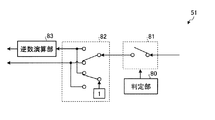
図2に戻って補正部32の説明を続ける。スイッチ部51は、例えば、電圧振幅Ugに含まれる振動成分ΔUgが閾値Uth以上である場合に、調整ゲインKを乗算部52、53または乗算部54、55へ出力する。
Returning to FIG. 2, the description of the
図6は、スイッチ部51の一例を示す図である。図6に示すように、スイッチ部51は、判定部80と、スイッチ81と、切替部82と、逆数演算部83とを備える。判定部80は、電圧振幅Ugに含まれる振動成分ΔUgが閾値Uth以上である場合に、スイッチ81をONにして調整ゲインKを出力し、振動成分ΔUgが閾値Uth未満である場合に、スイッチ81をOFFにして調整ゲインKの出力を停止する。なお、判定部80は、スイッチ81をOFFにして調整ゲインKの出力を停止する場合、例えば、調整ゲインKに代えて、「1」を出力する。また、スイッチ部51は、例えば、判定部80およびスイッチ81を設けない構成であってもよい。
FIG. 6 is a diagram illustrating an example of the
切替部82は、例えば、図示しない入力部から予め設定されたモードに基づき、調整ゲインKの出力先を切り替える。例えば、入力部からの設定が出力電流指令に対する補正を示す第1モードの場合、切替部82は、乗算部52、53に調整ゲインKを出力し、乗算部54、55には逆数演算部83経由で「1」を出力する。また、入力部からの設定が出力電流に対する補正を示す第2モードの場合、切替部82は、乗算部54、55に逆数演算部83経由で調整ゲインKを出力し、乗算部52、53には「1」を出力する。逆数演算部83は、調整ゲインKの逆数を演算し、調整ゲインKx(=1/K)として乗算部52、53へ出力する。なお、逆数演算部83は、切替部82から「1」が入力される場合、「1」を乗算部54、55へ出力する。
For example, the switching
なお、スイッチ部51は、図6に示す構成に限定されない。例えば、スイッチ部51は、切替部82を有しない構成であってもよく、この場合、調整ゲインKの出力先は、例えば、乗算部52、53と乗算部54、55とのいずれか一方である。
The
図2に戻って、補正部32の説明を続ける。乗算部52は、q軸電流指令Iq*にスイッチ部51から出力される調整ゲインKまたは「1」を乗算し、q軸電流指令Iq**として出力する。また、乗算部53は、d軸電流指令Id*にスイッチ部51から出力される調整ゲインKまたは「1」を乗算し、d軸電流指令Id**として出力する。Returning to FIG. 2, the description of the
また、乗算部54は、q軸電流Iqにスイッチ部51から出力される調整ゲインKxまたは「1」を乗算し、q軸電流Iq’として出力する。また、乗算部55は、d軸電流Idにスイッチ部51から出力される調整ゲインKxまたは「1」を乗算し、d軸電流Id’として出力する。なお、ゲイン調整部73、スイッチ部51および乗算部52〜55が補正処理部の一例に相当する。
The multiplying
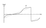
ここで、電力系統3に電圧異常が生じた場合について説明する。図7Aは、電力系統3の電圧異常の一例を示す図である。図7Aに示す例では、電力系統3のR相、S相およびV相電圧Vr、Vs、Vt(以下、系統相電圧Vr、Vs、Vtと記載する)がアンバランスである電圧異常を示す。
Here, the case where voltage abnormality arises in the electric power grid |
また、図7Bは、図7Aに示す電圧異常の状態で補正部32の補正がない場合の出力電流Ir、Is、Itの状態を示す図であり、図7Cは、図7Aに示す電圧異常の状態での電圧位相θの状態を示す図である。また、図7Dは、図7Aに示す電圧異常の状態で補正部32の補正がある場合の出力電流Ir、Is、Itの状態を示す図である。
FIG. 7B is a diagram illustrating the states of the output currents Ir, Is, It when the
図7Aに示すように、電力系統3に電圧異常が生じた場合、制御部23において補正部32がなければ、出力電流Ir、Is、Itは、図7Bに示すように、歪んだ状態になり、出力電流Ir、Is、Itに過度な脈動が生じる場合がある。その結果、過電流などが発生し、電力変換装置1の制御部23は、電力変換部10に対する制御を停止させてしまうおそれがある。
As shown in FIG. 7A, when a voltage abnormality occurs in the
このように、出力電流Ir、Is、Itに歪みが生じるのは、電圧異常の状態での電圧位相θが図7Cに示す状態になるためである。電圧正常時の状態での電圧位相θは図7Cにおいて破線で示す状態である。q軸電流指令Iq*およびd軸電流指令Id*は、電圧正常時の状態の電圧位相θを前提に生成されることから、q軸電流指令Iq*およびd軸電流指令Id*による電流制御後の電圧振幅指令Ug*が電圧異常時の電圧位相θによって電圧指令Vr*、Vs*、Vt*へ変換されることで、出力電流Ir、Is、Itが図7Bに示す状態になる。Thus, the distortion occurs in the output currents Ir, Is, It because the voltage phase θ in the state of abnormal voltage is in the state shown in FIG. 7C. The voltage phase θ when the voltage is normal is a state indicated by a broken line in FIG. 7C. Since the q-axis current command Iq * and the d-axis current command Id * are generated on the assumption of the voltage phase θ in the normal voltage state, after the current control by the q-axis current command Iq * and the d-axis current command Id * voltage amplitude command Ug * the voltage command Vr by voltage phase θ when a voltage abnormality *, Vs *, that is converted into Vt *, the output current Ir, is, it is the state shown in Figure 7B.
一方、電力系統3に電圧異常が生じた場合、制御部23は、q軸電流指令Iq*およびd軸電流指令Id*、または、q軸電流Iqおよびd軸電流Idを、補正部32により振動成分ΔUgに基づいて補正する。これにより、図7Dに示すように、出力電流Ir、Is、Itの歪みを抑制し、出力電流Ir、Is、Itに過度な脈動が生じることを抑制することができる。そのため、出力電流の精度を向上させることができ、電圧異常時において、例えば、不要解列の発生を抑制することができる。また、正常時の電圧位相θを保持して系統電圧異常時に切り替える場合に比べ、過電流の発生などを抑制でき、出力電流を精度よく制御することができる。On the other hand, when a voltage abnormality occurs in the
また、補正部32は、電圧振幅Ugと電圧振幅Ugから振動成分ΔUgを除去した電圧振幅Ug’との比率Rgを演算し、かかる比率Rgに基づいて、q軸電流指令Iq*およびd軸電流指令Id*、または、q軸電流Iqおよびd軸電流Idを補正する。電圧振幅Ugから振動成分ΔUgを除去した電圧振幅Ug’は、電力系統3の基本振幅電圧であり、比率Rgの振動成分ΔRgは、基本振幅電圧に対する振動成分ΔUgの比率である。Further, the
そのため、補正部32は、比率Rgの振動成分ΔRgに基づいて、q軸電流指令Iq*およびd軸電流指令Id*、または、q軸電流Iqおよびd軸電流Idを補正することで、適切な調整ゲインKにより出力電流の制御を行うことができ、出力電流の精度を向上させることができる。Therefore, the
また、補正部32は、電圧振幅Ugから振動成分ΔUgの除去をローパスフィルタ75で行うことができるため、振動成分ΔUgの除去を精度よく行いつつ、入力に対して出力を遅延させることができる。そのため、例えば、系統電圧異常の発生タイミングにおいて、比率Rgは、電圧低下後の電圧振幅Ugと電圧低下前の電圧振幅Ugで生成した電圧振幅Ug’との比率になる。これにより、系統電圧の低下率に応じた比率で出力電流を低減させることが可能となる。また、ローパスフィルタ75の時定数を大きくすることによって、系統電圧の低下率に応じて出力電流を抑える期間を長くすることができる。
Further, since the correcting
また、補正部32は、電圧振幅Ugから振動成分ΔUgの除去を移動平均演算部76で行うことができるため、振動成分ΔUgの除去を精度よく行うことができる。また、ローパスフィルタ75の場合と同様に、系統電圧異常の発生タイミングにおいて、比率Rgは、電圧低下後の電圧振幅Ugと電圧低下前の電圧振幅Ugで生成した電圧振幅Ug’との比率になるため、系統電圧の低下率に応じた比率で出力電流を低下させることが可能となる。なお、移動平均の期間を長くすることによって、系統電圧の低下率に応じた比率で出力電流を低減させる期間を長くすることができる。
Further, since the
また、補正部32は、電力系統3の電圧異常が発生する前の電圧振幅Ug(以下、電圧振幅Ugmと記載する)を記憶する電圧振幅記憶部77を有しており、電力系統3の電圧異常が発生した場合、比率Rgとして、電圧振幅Ugと電圧振幅Ugmとの比を演算する。これにより、系統電圧が低下した場合に、系統電圧の低下率に応じた比率で出力電流を低減させることが可能となる。なお、補正部32は、電力系統3の電圧異常が発生する前にローパスフィルタ75や移動平均演算部76によって振動成分ΔUgが除去された電圧振幅Ugを電圧振幅Ugmとして電圧振幅記憶部77に記憶することもできる。
The
また、電力系統3の電圧異常が発生する前は、系統相電圧Vr、Vs、Vtはバランスされており、三相平衡の状態であるため、電圧振幅Ugに含まれる振動成分ΔUgを無視することができる。そのため、電力系統3が正常である状態から継続して補正部32を動作させることができる。この場合、系統電圧異常が発生しても、制御部23における処理を変更することなく、電圧異常が発生したタイミングから迅速に系統電圧異常に対する処理を行うことができ、出力電流を精度よく制御することができる。一方、正常時の電圧位相θを保持して系統電圧異常時に切り替える場合、電圧異常が発生したタイミングから系統電圧異常と判定するまでの間、出力電流を精度よく制御することが難しい。
Before the voltage abnormality of the
また、スイッチ部51は、電圧振幅Ugに含まれる振動成分ΔUgが閾値Uth以上である場合に、調整ゲインKを出力し、振動成分ΔUgが閾値Uth未満である場合、調整ゲインKの出力を停止する。電力変換装置1に接続する電力系統3によっては、例えば、送電環境等の問題により電圧振幅Ugに含まれる振動成分ΔUgが大きくなるおそれがある。このような場合、制御部23は、補正部32による補正処理を停止させることができる。これにより、電力系統3が正常時にも関わらず電圧振幅Ugに含まれる振動成分ΔUgが大きい場合に、補正部32の補正による影響を排除することができる。なお、例えば、電力系統3が正常時に補正部32による補正による影響が少ない場合などにおいては、スイッチ部51を設けなくても構わない。
The
上述した補正部32は、電圧振幅Ugと電圧振幅Ugから振動成分ΔUgを除去した電圧振幅Ug’との比率Rgを演算し、かかる比率Rgに基づいて、出力電流の制御を行うが、補正部32は、比率Rgを用いない構成であってもよい。図8は、補正部32の他の構成例を示す図である。
The
図8に示すように、振動成分抽出部84と、ゲイン調整部85と、スイッチ部86と、減算部87と、電圧振幅記憶部88と、比率演算部89と、加算部90、91と、乗算部92、93と、調整値補正部94とを備える。
As shown in FIG. 8, the vibration
振動成分抽出部84は、位相・振幅検出部20により取得された電圧振幅Ugから振動成分ΔUgを抽出する。かかる振動成分抽出部84は、例えば、ハイパスフィルタによって構成される。ゲイン調整部85は、振動成分抽出部84によって抽出された振動成分ΔUgにゲインK2を乗算して調整値Kiを求める。
The vibration
スイッチ部86は、電圧振幅Ugに含まれる振動成分ΔUgが閾値Uth以上である場合に、調整値Kiを加算部90、91へ出力する。スイッチ部86は、判定部95と、スイッチ96とを備える。判定部95は、判定部80と同様に、振動成分ΔUgが閾値Uth以上であるか否かを判定し、スイッチ96を制御する。なお、補正部32は、スイッチ部86を設けない構成であってもよい。
The
加算部90は、調整値Kiをq軸電流指令Iq*に加算する。また、加算部91は、調整値補正部94によって補正された調整値Ki’をd軸電流指令Id*に加算する。調整値補正部94は、例えば、下記式(14)の演算を行うことにより、調整値Ki’を求める。
Ki’=Ki×(Id*/Iq*) ・・・(14)
Ki ′ = Ki × (Id * / Iq * ) (14)
このように、図8に示す補正部32は、振動成分ΔUgに応じた調整値Kiを生成し、かかる調整値Kiに基づいてq軸電流指令Iq*およびd軸電流指令Id*を補正する。これにより、出力電流の歪みを抑制し、出力電流に過度な脈動が生じることを抑制することができる。なお、図8に示す例では、調整値Kiに基づいてq軸電流指令Iq*およびd軸電流指令Id*を補正するが、調整値Kiの逆数に基づいてq軸電流Iqおよびd軸電流Idを補正する構成を補正部32に設けることもできる。As described above, the
減算部87は、電圧振幅Ugから振動成分ΔUgを減算することによって、電圧振幅Ugから振動成分ΔUgを除去した電圧振幅Ug’を演算する。電圧振幅記憶部88は、例えば、電圧異常検出部22から異常検出信号Sdが出力されるまで、電圧振幅記憶部77と同様に、周期的に記憶する電圧振幅Ug’を更新し、電圧異常検出部22から異常検出信号Sdが出力された後は、記憶する電圧振幅Ug’の更新を停止する。
The
比率演算部89は、比率演算部72と同様に、減算部87により電圧振幅Ugから振動成分ΔUgを除去した電圧振幅Ug’と電圧振幅記憶部88に記憶された電圧振幅Ug’との比率Rgを演算する。乗算部92は、加算部90の加算結果に比率Rgを乗じてq軸電流指令Iq**を生成する。また、乗算部93は、加算部91の加算結果に比率Rgを乗じてd軸電流指令Id**を生成する。これにより、系統電圧の低下率に応じた比率で出力電流を低減することが可能となる。なお、補正部32は、減算部87、電圧振幅記憶部88、比率演算部89および乗算部92、93を設けない構成であってもよい。なお、ゲイン調整部85、スイッチ部86、加算部90、91および調整値補正部94が補正処理部の一例に相当する。Similarly to the
図2に示す電力変換装置1では、昇圧回路16およびインバータ回路17が電力変換部10である例を示したが、電力変換装置1の電力変換部10は、図2に示す構成に限定されない。例えば、電力変換装置1は、図9に示すように、複数の双方向スイッチSw1〜Sw9を含む電力変換部10を備えるマトリクスコンバータであってもよい。図9は、電力変換部10の一例を示す図であり、複数の双方向スイッチSw1〜Sw9は、発電装置2の各相と電力系統3の各相との間を接続するスイッチである。かかる双方向スイッチSw1〜Sw9は、導通方向が制御可能な複数のスイッチング素子(例えば、MOSFETやIGBT)などから構成される。
In the
なお、上述した例では、q軸とd軸の電流補正を行ったが、電力変換装置1は、例えば、力率1制御の場合、q軸のみの電流補正を行うこともできる。
In the above-described example, the current correction of the q axis and the d axis is performed. However, for example, in the case of
[4.電流制御フロー]
ここで、制御部23により実行される出力電流制御処理の一例について図10を参照して具体的に説明する。図10は、制御部23により実行される電力変換処理の一例を示すフローチャートである。[4. Current control flow]
Here, an example of the output current control process executed by the
図10に示すように、位相・振幅検出部20は、電力系統3の電圧振幅Ugを取得する(ステップS10)。制御部23は、電圧振幅Ugの振動成分ΔUgに基づいて、出力電流指令(q軸電流指令Iq*およびd軸電流指令Id*)および出力電流値(q軸電流Iqおよびd軸電流Id)のうちの一方を補正する(ステップS11)。As shown in FIG. 10, the phase /
制御部23は、出力電流指令および出力電流値のうちの他方と補正後の一方との差に基づいて電力変換部10を制御することにより、電力変換部10から電力系統3への出力電流を制御する(ステップS12)。
The
以上のように、実施形態に係る電力変換装置1は、電圧振幅Ugの振動成分ΔUgに基づいて、出力電流指令および出力電流値のうちの一方を補正することから、過電流の発生などを抑制でき、出力電流を精度よく制御することができる。
As described above, the
[5.その他]
図1および図2に示す電力変換装置1は、電力変換部10を含む構成であるが、電力変換部10を制御する制御装置として、例えば、以下の構成を有するようにしてもよい。
(構成例)
電力系統3の電圧振幅Ugを取得する電圧振幅取得部と、
前記電圧振幅取得部により取得された前記電圧振幅Ugの振動成分ΔUgに基づいて、前記電力系統3への出力電流を制御する指令Uq*、Ud*(出力電圧指令の一例)を生成する制御部23と、を備え、
前記制御部23は、
前記電力系統3への出力電流Iq、Idを取得する電流取得部と、
前記電圧振幅取得部により取得された前記電圧振幅Ugの振動成分ΔUgに基づいて、出力電流指令Iq*、Id*または前記電流取得部によって検出された前記出力電流Iq、Idを補正する補正部と、
前記補正部によって補正された前記出力電流指令Iq*、Id*または前記出力電流Iq、Idに基づいて前記電力系統3への出力電流を制御する指令Uq*、Ud*(出力電圧指令の一例)を生成する電流制御部と、
ことを特徴とする記載の制御装置。[5. Others]
Although the
(Configuration example)
A voltage amplitude acquisition unit that acquires the voltage amplitude Ug of the
A control unit that generates commands Uq * and Ud * (an example of an output voltage command) for controlling the output current to the
The
A current acquisition unit for acquiring output currents Iq and Id to the
A correction unit for correcting the output current commands Iq * and Id * or the output currents Iq and Id detected by the current acquisition unit based on the vibration component ΔUg of the voltage amplitude Ug acquired by the voltage amplitude acquisition unit; ,
Commands Uq * , Ud * (an example of an output voltage command) for controlling the output current to the
A control device according to claim.
さらなる効果や変形例は、当業者によって容易に導き出すことができる。このため、本発明のより広範な態様は、以上のように表しかつ記述した特定の詳細および代表的な実施形態に限定されるものではない。したがって、添付の特許請求の範囲およびその均等物によって定義される総括的な発明の概念の精神または範囲から逸脱することなく、様々な変更が可能である。 Further effects and modifications can be easily derived by those skilled in the art. Thus, the broader aspects of the present invention are not limited to the specific details and representative embodiments shown and described above. Accordingly, various modifications can be made without departing from the spirit or scope of the general inventive concept as defined by the appended claims and their equivalents.
1 電力変換装置
2 発電装置
3 電力系統
10 電力変換部
11、13、14 電圧検出部
12、15 電流検出部
20 位相・振幅検出部
21 dq演算部
22 電圧異常検出部
23 制御部
31 電流指令生成部
32 補正部
33 電流制御部
34 電圧指令生成部
35 PWM制御部
41、61、62、87 減算部
42 q軸指令生成部
43 無効成分電流演算部
50 ゲイン演算部
51、83、86 スイッチ部
52〜55、92、93 乗算部
63 q軸電流制御部
64 d軸電流制御部
78、79、83 切替部
71 振動成分除去部
72、89 比率演算部
73、85 ゲイン調整部
75 ローパスフィルタ
76 移動平均演算部
77、88 電圧振幅記憶部
80、95 判定部
81、96 スイッチ
84 振動成分抽出部
90、91 加算部
94 調整値補正部
100 発電システムDESCRIPTION OF
Claims (11)
前記電力系統の電圧振幅を取得する電圧振幅取得部と、
前記電圧振幅取得部により取得された前記電圧振幅の振動成分に基づいて、前記電力変換部から前記電力系統への出力電流を制御する制御部と、
前記電力変換部から前記電力系統への出力電流を検出する電流検出部と、を備え、
前記制御部は、
前記電圧振幅取得部により取得された前記電圧振幅の振動成分に基づいて、出力電流指令または前記電流検出部によって検出された前記出力電流を補正する補正部と、
前記補正部によって補正された前記出力電流指令または前記出力電流に基づいて前記電力変換部から前記電力系統への出力電流を制御する電流制御部と、を備え、
前記補正部は、
前記電圧振幅取得部によって取得された前記電圧振幅から前記振動成分を除去する振動成分除去部と、
前記電圧振幅取得部により取得された前記電圧振幅と前記振動成分除去部により前記振動成分が除去された前記電圧振幅との比率を演算する比率演算部と、
前記比率演算部による演算結果に基づいて、前記出力電流指令または前記電流検出部によって検出された前記出力電流を補正する補正処理部と、を備える
ことを特徴とする電力変換装置。 A power converter connected to the power system;
A voltage amplitude acquisition unit for acquiring a voltage amplitude of the power system;
Based on the vibration component of the voltage amplitude acquired by the voltage amplitude acquisition unit, a control unit for controlling the output current from the power conversion unit to the power system;
A current detection unit that detects an output current from the power conversion unit to the power system ,
The controller is
A correction unit for correcting the output current command or the output current detected by the current detection unit based on the vibration component of the voltage amplitude acquired by the voltage amplitude acquisition unit;
A current control unit that controls an output current from the power conversion unit to the power system based on the output current command or the output current corrected by the correction unit, and
The correction unit is
A vibration component removing unit that removes the vibration component from the voltage amplitude obtained by the voltage amplitude obtaining unit;
A ratio calculation unit that calculates a ratio between the voltage amplitude acquired by the voltage amplitude acquisition unit and the voltage amplitude from which the vibration component has been removed by the vibration component removal unit;
A power conversion device comprising: a correction processing unit that corrects the output current detected by the output current command or the current detection unit based on a calculation result by the ratio calculation unit .
前記電圧振幅の移動平均を演算することによって前記電圧振幅から前記振動成分を除去する
ことを特徴とする請求項1に記載の電力変換装置。 The vibration component removing unit is
The power converter according to claim 1 , wherein the vibration component is removed from the voltage amplitude by calculating a moving average of the voltage amplitude.
前記電圧振幅から前記振動成分を除去するローパスフィルタである
ことを特徴とする請求項1に記載の電力変換装置。 The vibration component removing unit is
The power converter according to claim 1 , wherein the power converter is a low-pass filter that removes the vibration component from the voltage amplitude.
前記出力電流指令または前記電流検出部によって検出された前記出力電流に対して前記比率演算部による演算結果に応じた値を乗算する乗算部を備える
ことを特徴とする請求項1〜3のいずれか1つに記載の電力変換装置。 The correction processing unit
Any one of claims 1 to 3, characterized in that it comprises a multiplication unit for multiplying a value corresponding to the calculation result of said ratio calculating unit relative to said detected output current by the output current command or the current detector The power converter as described in one.
前記電力系統の電圧振幅を取得する電圧振幅取得部と、
前記電圧振幅取得部により取得された前記電圧振幅の振動成分に基づいて、前記電力変換部から前記電力系統への出力電流を制御する制御部と、
前記電力変換部から前記電力系統への出力電流を検出する電流検出部と、を備え、
前記制御部は、
前記電圧振幅取得部により取得された前記電圧振幅の前記振動成分に基づいて、出力電流指令または前記電流検出部によって検出された前記出力電流を補正する補正部と、
前記補正部によって補正された前記出力電流指令または前記出力電流に基づいて前記電力変換部から前記電力系統への出力電流を制御する電流制御部と、を備え、
前記補正部は、
前記電圧振幅取得部によって取得された前記電圧振幅から前記電力系統の基本周波数の成分を除いて前記振動成分を抽出する振動成分抽出部と、
前記振動成分抽出部によって抽出された前記振動成分に基づいて、前記出力電流指令または前記電流検出部によって検出された前記出力電流を補正する補正処理部と、を備える
ことを特徴とする電力変換装置。 A power converter connected to the power system;
A voltage amplitude acquisition unit for acquiring a voltage amplitude of the power system;
Based on the vibration component of the voltage amplitude acquired by the voltage amplitude acquisition unit, a control unit for controlling the output current from the power conversion unit to the power system;
A current detection unit that detects an output current from the power conversion unit to the power system,
The controller is
A correction unit that corrects the output current command or the output current detected by the current detection unit based on the vibration component of the voltage amplitude acquired by the voltage amplitude acquisition unit;
A current control unit that controls an output current from the power conversion unit to the power system based on the output current command or the output current corrected by the correction unit, and
The correction unit is
A vibration component extraction unit that extracts the vibration component by removing the fundamental frequency component of the power system from the voltage amplitude acquired by the voltage amplitude acquisition unit;
Wherein based on the vibration component extracted by the vibration component extracting unit, the output current command or correction unit and, power you characterized in that it comprises a for correcting the output current detected by the current detection unit Conversion device.
前記出力電流指令または前記電流検出部によって検出された前記出力電流に対して前記振動成分抽出部により抽出された前記振動成分に応じた値を加算する加算部を備える
ことを特徴とする請求項5に記載の電力変換装置。 The correction processing unit
Claim, characterized in that it comprises an adder for adding a value corresponding to the vibration component extracted by the vibration component extracting unit relative to said detected output current by the output current command or the current detector 5 The power converter device described in 1.
前記電圧振幅取得部によって取得された前記電圧振幅から前記振動成分を除去する振動成分除去部と、
前記振動成分除去部により前記振動成分が除去された前記電圧振幅を記憶する電圧振幅記憶部を備え、
前記振動成分除去部により前記振動成分が除去された前記電圧振幅と前記電圧振幅記憶部によって記憶された前記電圧振幅との比率を演算する比率演算部と、
前記出力電流指令または前記電流検出部によって検出された前記出力電流に対して前記比率演算部による演算結果に応じた値を乗算する乗算部と、を備える
ことを特徴とする請求項5または6に記載の電力変換装置。 The correction unit is
A vibration component removing unit that removes the vibration component from the voltage amplitude obtained by the voltage amplitude obtaining unit;
A voltage amplitude storage unit that stores the voltage amplitude from which the vibration component has been removed by the vibration component removal unit;
A ratio calculation unit that calculates a ratio between the voltage amplitude from which the vibration component has been removed by the vibration component removal unit and the voltage amplitude stored by the voltage amplitude storage unit;
A multiplying unit for multiplying a value corresponding to the calculation result of said ratio calculating unit relative to said detected output current by the output current command or the current detector, to claim 5 or 6, characterized in that it comprises The power converter described.
前記電圧振幅取得部により取得された前記電圧振幅または前記電圧振幅の振動成分が閾値以上であるか否かを判定する判定部と、
前記判定部によって前記電圧振幅または前記電圧振幅の振動成分が閾値以上であると判定された場合に、前記電圧振幅の振動成分に基づいて、前記出力電流指令または前記電流検出部によって検出された前記出力電流を補正する
ことを特徴とする請求項1〜7のいずれか1つに記載の電力変換装置。 The correction unit is
A determination unit that determines whether the voltage amplitude acquired by the voltage amplitude acquisition unit or a vibration component of the voltage amplitude is greater than or equal to a threshold;
When the determination unit determines that the voltage amplitude or the vibration component of the voltage amplitude is greater than or equal to a threshold, the output current command or the current detection unit detected based on the vibration component of the voltage amplitude power converter according to any one of claims 1 to 7, wherein the correcting the output current.
前記電力変換装置は、前記発電源によって発電された電力を前記電力系統へ出力する
ことを特徴とする発電システム。 A power conversion device according to any one of claims 1 to 8 , and a power generation source connected to the power conversion device,
The power conversion apparatus outputs the power generated by the power generation source to the power system.
前記電力変換部から前記電力系統への出力電流を検出することと
前記取得された前記電圧振幅から当該電圧振幅の振動成分を除去することと、
前記取得された前記電圧振幅と前記振動成分が除去された前記電圧振幅との比率を演算することと、
前記演算された前記比率に基づいて、出力電流指令または前記検出された出力電流を補正することと、
前記補正された前記出力電流指令または前記出力電流に基づいて前記電力変換部から前記電力系統への出力電流を制御することと、を含む
ことを特徴とする電流制御方法。 Obtaining the voltage amplitude of the power grid connected to the power converter;
Detecting an output current from the power converter to the power system;
Removing a vibration component of the voltage amplitude from the acquired voltage amplitude;
Calculating a ratio between the acquired voltage amplitude and the voltage amplitude from which the vibration component has been removed;
Correcting the output current command or the detected output current based on the calculated ratio;
Controlling an output current from the power conversion unit to the power system based on the corrected output current command or the output current . A current control method comprising:
前記電力変換部から前記電力系統への出力電流を検出することとDetecting an output current from the power converter to the power system;
前記取得された前記電圧振幅から前記電力系統の基本周波数の成分を除いて前記電圧振幅の振動成分を抽出することと、Extracting a vibration component of the voltage amplitude by removing a component of the fundamental frequency of the power system from the acquired voltage amplitude;
前記抽出された前記振動成分に基づいて、出力電流指令または前記検出された出力電流を補正することと、Correcting the output current command or the detected output current based on the extracted vibration component;
前記補正された前記出力電流指令または前記出力電流に基づいて前記電力変換部から前記電力系統への出力電流を制御することと、を含むControlling an output current from the power converter to the power system based on the corrected output current command or the output current.
ことを特徴とする電流制御方法。A current control method.
Applications Claiming Priority (1)
| Application Number | Priority Date | Filing Date | Title |
|---|---|---|---|
| PCT/JP2014/076081 WO2016051500A1 (en) | 2014-09-30 | 2014-09-30 | Power conversion device, power generation system, and current control method |
Publications (2)
| Publication Number | Publication Date |
|---|---|
| JP6103155B2 true JP6103155B2 (en) | 2017-03-29 |
| JPWO2016051500A1 JPWO2016051500A1 (en) | 2017-04-27 |
Family
ID=55629598
Family Applications (1)
| Application Number | Title | Priority Date | Filing Date |
|---|---|---|---|
| JP2016551383A Active JP6103155B2 (en) | 2014-09-30 | 2014-09-30 | Power converter, power generation system, and current control method |
Country Status (3)
| Country | Link |
|---|---|
| US (1) | US10516330B2 (en) |
| JP (1) | JP6103155B2 (en) |
| WO (1) | WO2016051500A1 (en) |
Families Citing this family (7)
| Publication number | Priority date | Publication date | Assignee | Title |
|---|---|---|---|---|
| JP6237852B1 (en) * | 2016-09-30 | 2017-11-29 | ダイキン工業株式会社 | Active filter control device |
| KR101904101B1 (en) * | 2016-12-26 | 2018-10-05 | 효성중공업 주식회사 | Method for removing DC component of MMC converter output |
| JP7118783B2 (en) * | 2018-07-12 | 2022-08-16 | 新電元工業株式会社 | Grid-connected inverter device |
| WO2020204010A1 (en) * | 2019-03-29 | 2020-10-08 | 国立大学法人東北大学 | Electric power converting device, and electricity generating system |
| US20240014661A1 (en) * | 2020-11-17 | 2024-01-11 | Mitsubishi Electric Corporation | Power conversion device and estimation device |
| US11735908B2 (en) * | 2021-02-15 | 2023-08-22 | Schweitzer Engineering Laboratories, Inc. | Dependable open-phase detection in electric power delivery systems with inverter-based resources |
| CN114188954A (en) * | 2021-11-10 | 2022-03-15 | 华为数字能源技术有限公司 | Power oscillation suppression method, system, controller and storage medium |
Family Cites Families (22)
| Publication number | Priority date | Publication date | Assignee | Title |
|---|---|---|---|---|
| US5532569A (en) * | 1987-06-03 | 1996-07-02 | Hitachi, Ltd. | Inverter control apparatus |
| JP3432882B2 (en) * | 1994-02-25 | 2003-08-04 | 三洋電機株式会社 | Islanding detection method |
| US6154379A (en) * | 1998-07-16 | 2000-11-28 | Tdk Corporation | Electric power conversion device |
| JP4056852B2 (en) * | 2002-10-31 | 2008-03-05 | 株式会社日立製作所 | Power converter |
| JP4367279B2 (en) * | 2004-07-14 | 2009-11-18 | 株式会社デンソー | Control device for synchronous motor |
| JP4815239B2 (en) * | 2006-03-22 | 2011-11-16 | 東芝三菱電機産業システム株式会社 | Control device for power conversion circuit |
| JP2008059968A (en) * | 2006-09-01 | 2008-03-13 | Matsushita Electric Ind Co Ltd | Fuel cell system |
| JP5387859B2 (en) * | 2008-05-30 | 2014-01-15 | 株式会社安川電機 | Matrix converter control device and output voltage generation method thereof |
| JP5292995B2 (en) * | 2008-08-22 | 2013-09-18 | 株式会社ジェイテクト | Motor control device and electric power steering device |
| KR101179784B1 (en) * | 2008-09-19 | 2012-09-04 | 미쓰비시덴키 가부시키가이샤 | Dc-dc converter |
| JP5447645B2 (en) * | 2010-03-03 | 2014-03-19 | 株式会社安川電機 | Inverter device and control method thereof |
| JP5664080B2 (en) * | 2010-09-28 | 2015-02-04 | 日産自動車株式会社 | Motor control device and motor control method |
| JP5300028B2 (en) * | 2010-12-28 | 2013-09-25 | オリジン電気株式会社 | Single-phase voltage type AC / DC converter and system interconnection system |
| JP5500141B2 (en) * | 2011-09-01 | 2014-05-21 | 株式会社安川電機 | Power converter |
| JP5760930B2 (en) | 2011-10-07 | 2015-08-12 | 日新電機株式会社 | Control device for power conversion device for grid connection, and power conversion device for grid connection |
| US8902616B2 (en) * | 2011-10-13 | 2014-12-02 | Rockwell Automation Technologies, Inc. | Active front end power converter with diagnostic and failure prevention using peak detector with decay |
| WO2013080744A1 (en) * | 2011-11-30 | 2013-06-06 | 株式会社安川電機 | Matrix converter |
| JP5993675B2 (en) * | 2012-09-14 | 2016-09-14 | 株式会社日立製作所 | Power converter, power conversion system, and control method for power converter |
| JP5712987B2 (en) * | 2012-09-27 | 2015-05-07 | ダイキン工業株式会社 | Power converter control method |
| US9329612B2 (en) * | 2012-10-05 | 2016-05-03 | Petra Solar, Inc. | Methods and systems for mitigation of intermittent generation impact on electrical power systems |
| JP5817947B1 (en) * | 2014-06-19 | 2015-11-18 | ダイキン工業株式会社 | Power conversion control device |
| JP6090275B2 (en) * | 2014-09-25 | 2017-03-08 | 株式会社デンソー | Power converter |
-
2014
- 2014-09-30 JP JP2016551383A patent/JP6103155B2/en active Active
- 2014-09-30 WO PCT/JP2014/076081 patent/WO2016051500A1/en active Application Filing
-
2017
- 2017-03-30 US US15/473,880 patent/US10516330B2/en active Active
Also Published As
| Publication number | Publication date |
|---|---|
| US20170207698A1 (en) | 2017-07-20 |
| JPWO2016051500A1 (en) | 2017-04-27 |
| WO2016051500A1 (en) | 2016-04-07 |
| US10516330B2 (en) | 2019-12-24 |
Similar Documents
| Publication | Publication Date | Title |
|---|---|---|
| JP6103155B2 (en) | Power converter, power generation system, and current control method | |
| US9484839B2 (en) | Power converter, power generating system, apparatus for controlling power converter, and method for controlling power converter | |
| US9509233B2 (en) | Power converter, power generation system, control apparatus, and power conversion method | |
| JP6735827B2 (en) | Power converter | |
| JP5985775B1 (en) | Isolated operation detection device and isolated operation detection method | |
| EP3439163B1 (en) | Power converter | |
| KR101929519B1 (en) | Three level neutral point clamped inverter system having imbalance capacitor voltages and its control method | |
| EP2837942A1 (en) | Ground fault detecting circuit and power conversion device using same | |
| JP2008306829A (en) | Harmonic current compensator | |
| JP6848622B2 (en) | Power converter and its control device | |
| JP2004201440A (en) | Method and apparatus for pulse width modulation, power conversion method, and power converter | |
| KR101380380B1 (en) | Method of adaptive phase tracking depending on the state of power system and system for it | |
| JP5888074B2 (en) | Power converter | |
| JP5351390B2 (en) | Power converter | |
| US11063530B2 (en) | Method for removing direct current component at output terminal of MMC converter | |
| JP6304180B2 (en) | Power conversion device, power generation system, control device, and control method | |
| JP2017005811A (en) | Power conversion device and current detection method | |
| JP2014187742A (en) | Inverter device | |
| JP6337688B2 (en) | Power conversion device, power generation system, and power conversion method | |
| JP4176709B2 (en) | AC / DC bidirectional converter | |
| US20140239716A1 (en) | Ac power supply apparatus | |
| WO2021070295A1 (en) | Power conversion device | |
| JP2007006700A (en) | Power conversion apparatus |
Legal Events
| Date | Code | Title | Description |
|---|---|---|---|
| A975 | Report on accelerated examination |
Free format text: JAPANESE INTERMEDIATE CODE: A971005 Effective date: 20161025 |
|
| A131 | Notification of reasons for refusal |
Free format text: JAPANESE INTERMEDIATE CODE: A131 Effective date: 20161101 |
|
| A521 | Request for written amendment filed |
Free format text: JAPANESE INTERMEDIATE CODE: A523 Effective date: 20161226 |
|
| TRDD | Decision of grant or rejection written | ||
| A01 | Written decision to grant a patent or to grant a registration (utility model) |
Free format text: JAPANESE INTERMEDIATE CODE: A01 Effective date: 20170131 |
|
| A61 | First payment of annual fees (during grant procedure) |
Free format text: JAPANESE INTERMEDIATE CODE: A61 Effective date: 20170213 |
|
| R150 | Certificate of patent or registration of utility model |
Ref document number: 6103155 Country of ref document: JP Free format text: JAPANESE INTERMEDIATE CODE: R150 |