JP4919552B2 - Game machine - Google Patents
Game machine Download PDFInfo
- Publication number
- JP4919552B2 JP4919552B2 JP2001225206A JP2001225206A JP4919552B2 JP 4919552 B2 JP4919552 B2 JP 4919552B2 JP 2001225206 A JP2001225206 A JP 2001225206A JP 2001225206 A JP2001225206 A JP 2001225206A JP 4919552 B2 JP4919552 B2 JP 4919552B2
- Authority
- JP
- Japan
- Prior art keywords
- output
- data
- power supply
- command
- signal
- Prior art date
- Legal status (The legal status is an assumption and is not a legal conclusion. Google has not performed a legal analysis and makes no representation as to the accuracy of the status listed.)
- Expired - Fee Related
Links
- 238000000034 method Methods 0.000 claims description 444
- 230000008569 process Effects 0.000 claims description 439
- 238000012545 processing Methods 0.000 claims description 132
- 238000011084 recovery Methods 0.000 claims description 52
- 238000013500 data storage Methods 0.000 claims description 38
- 230000004044 response Effects 0.000 claims description 17
- 230000008859 change Effects 0.000 claims description 10
- 239000000872 buffer Substances 0.000 description 93
- 230000005540 biological transmission Effects 0.000 description 54
- 238000001514 detection method Methods 0.000 description 47
- 238000010586 diagram Methods 0.000 description 38
- 238000012544 monitoring process Methods 0.000 description 37
- 230000015654 memory Effects 0.000 description 35
- 230000007246 mechanism Effects 0.000 description 19
- 238000004364 calculation method Methods 0.000 description 17
- 230000006870 function Effects 0.000 description 15
- 238000005034 decoration Methods 0.000 description 9
- 239000003990 capacitor Substances 0.000 description 8
- 238000004458 analytical method Methods 0.000 description 6
- 238000012790 confirmation Methods 0.000 description 6
- 230000007423 decrease Effects 0.000 description 6
- 230000000694 effects Effects 0.000 description 6
- 239000000758 substrate Substances 0.000 description 6
- 239000011521 glass Substances 0.000 description 5
- 238000013481 data capture Methods 0.000 description 4
- 238000003780 insertion Methods 0.000 description 4
- 230000037431 insertion Effects 0.000 description 4
- 238000012986 modification Methods 0.000 description 4
- 230000004048 modification Effects 0.000 description 4
- 238000004904 shortening Methods 0.000 description 4
- 230000005284 excitation Effects 0.000 description 3
- 230000002093 peripheral effect Effects 0.000 description 3
- 230000000630 rising effect Effects 0.000 description 3
- 238000010304 firing Methods 0.000 description 2
- 238000005259 measurement Methods 0.000 description 2
- 238000011144 upstream manufacturing Methods 0.000 description 2
- 239000002699 waste material Substances 0.000 description 2
- 230000005856 abnormality Effects 0.000 description 1
- 230000004913 activation Effects 0.000 description 1
- 230000003321 amplification Effects 0.000 description 1
- 239000011324 bead Substances 0.000 description 1
- 230000008033 biological extinction Effects 0.000 description 1
- 230000015572 biosynthetic process Effects 0.000 description 1
- 230000004397 blinking Effects 0.000 description 1
- 238000004891 communication Methods 0.000 description 1
- 238000013461 design Methods 0.000 description 1
- 238000003745 diagnosis Methods 0.000 description 1
- 239000000284 extract Substances 0.000 description 1
- 238000009434 installation Methods 0.000 description 1
- 230000002427 irreversible effect Effects 0.000 description 1
- 239000004973 liquid crystal related substance Substances 0.000 description 1
- 238000007726 management method Methods 0.000 description 1
- 238000003199 nucleic acid amplification method Methods 0.000 description 1
- 230000010355 oscillation Effects 0.000 description 1
- 230000002265 prevention Effects 0.000 description 1
- 238000004886 process control Methods 0.000 description 1
- 230000001681 protective effect Effects 0.000 description 1
- 238000004092 self-diagnosis Methods 0.000 description 1
- 230000008054 signal transmission Effects 0.000 description 1
- 230000005236 sound signal Effects 0.000 description 1
- 238000003786 synthesis reaction Methods 0.000 description 1
- 230000001960 triggered effect Effects 0.000 description 1
- 238000010977 unit operation Methods 0.000 description 1
- 229910000859 α-Fe Inorganic materials 0.000 description 1
Images


Landscapes
- Pinball Game Machines (AREA)
- Display Devices Of Pinball Game Machines (AREA)
Description
【0001】
【発明の属する技術分野】
本発明は、遊技者が遊技媒体を用いて所定の遊技を行うことが可能なパチンコ遊技機やスロットマシン等の遊技機に関する。
【0002】
【従来の技術】
遊技機として、遊技球などの遊技媒体を発射装置によって遊技領域に発射し、遊技領域に設けられている入賞口などの入賞領域に遊技媒体が入賞すると、所定個の賞球が遊技者に払い出されるものがある。さらに、表示状態が変化可能な可変表示装置が設けられ、可変表示装置の表示結果があらかじめ定められた特定の表示態様となった場合に所定の遊技価値を遊技者に与えるように構成されたものがある。
【0003】
特別図柄を表示する可変表示装置の表示結果があらかじめ定められた特定の表示態様の組合せとなることを、通常、「大当り」という。なお、遊技価値とは、遊技機の遊技領域に設けられた可変入賞球装置の状態が打球が入賞しやすい遊技者にとって有利な状態になることや、遊技者にとって有利な状態となるための権利を発生させたりすることである。
【0004】
大当りが発生すると、例えば、大入賞口が所定回数開放して打球が入賞しやすい大当り遊技状態に移行する。そして、各開放期間において、所定個(例えば10個)の大入賞口への入賞があると大入賞口は閉成する。そして、大入賞口の開放回数は、所定回数(例えば16ラウンド)に固定されている。なお、各開放について開放時間(例えば29.5秒)が決められ、入賞数が所定個に達しなくても開放時間が経過すると大入賞口は閉成する。また、大入賞口が閉成した時点で所定の条件(例えば、大入賞口内に設けられているVゾーンへの入賞)が成立していない場合には、大当り遊技状態は終了する。
【0005】
そして、遊技球が遊技盤に設けられている入賞口に遊技球が入賞すると、あらかじめ決められている個数の賞球払出が行われる。遊技の進行は主基板に搭載された遊技制御手段によって制御されるので、入賞にもとづく賞球個数は、遊技制御手段によって決定され、景品としての遊技球を払い出す払出機構を制御する払出制御手段に送信される。なお、以下、遊技制御手段およびその他の制御手段を、それぞれ電気部品制御手段と呼ぶことがある。また、電気部品とは、遊技機に設けられている部品(機構部品や回路等)であって、電気的に動作するものである。
【0006】
【発明が解決しようとする課題】
遊技機には、遊技制御手段を初めとする種々の電気部品制御手段が搭載されているが、一般に、各電気部品制御手段はマイクロコンピュータで構成される。すなわち、ROM等にプログラムが格納され、制御上一時的に発生するデータや制御進行に伴って変化するデータがRAMに格納される。すると、遊技機に停電等による電源断状態が発生すると、RAM内のデータは失われてしまう。よって、停電等からの復旧時には、最初の状態(例えば、遊技店においてその日最初に遊技機に電源投入されたときの状態)に戻さざるを得ないので、遊技者に不利益がもたらされる可能性がある。例えば、大当り遊技中において電源断が発生し遊技機が最初の状態に戻ってしまうのでは、遊技者は大当りの発生にもとづく利益を享受することができなくなってしまう。
【0007】
そのような事態を回避するには、停電等の不測の電力供給の停止が生じたときに、電気部品制御手段において、必要なデータを電源バックアップされたバックアップRAMに保存し、電源が復旧したときに保存されていたデータを復元して制御状態を復元し遊技を再開させればよい。しかし、それぞれに電気部品制御手段が搭載された電気部品制御基板が複数ある場合には各電気部品制御手段間でコマンドの送受信を行う必要があるが、コマンドの送受信を行っている最中に電力供給の停止が生じた場合には、コマンドの送受信が完了しないまま、電気部品制御手段が動作を停止してしまうおそれがある。
【0008】
そのような状況が生ずると、電源が復旧したときに、保存されていたデータにもとづいて制御状態を電力供給停止前の状態に戻しても、1つのコマンドの送受信が欠落してしまったことになる。そのコマンドが、遊技者の利益に直結するような情報(例えば、遊技制御手段から電気部品制御手段としての払出制御手段に賞球払出を指示するための情報)を含んでいるような場合には、遊技者に不利益が与えられてしまうことになる。
【0009】
そこで、本発明は、停電等の不測の電力供給の停止が生じたときに制御状態を復旧させるために必要なデータを保存するための電力供給停止時処理を実行することが可能な遊技機において、遊技制御手段と他の電気部品制御手段との間におけるコマンドの送受信を欠落させないようにすることができる遊技機を提供することを目的とする。
【0010】
【課題を解決するための手段】
本発明による遊技機は、遊技者が遊技媒体を用いて所定の遊技を行うことが可能な遊技機であって、遊技機への電力供給が停止しても所定期間は記憶内容を保持することが可能な変動データ記憶手段(例えばバックアップRAM)を有し、遊技の進行に関わる制御を行う遊技制御手段(例えばCPU56等)と、遊技制御手段からのコマンドにもとづいて遊技機に設けられている電気部品の制御を行う電気部品制御手段(例えば払出制御手段)とを備え、遊技制御手段が、コマンドデータを出力ポートを介して出力する処理を実行した後、コマンドデータの電気部品制御手段への入力を指示するための指示信号(例えば図23における割込信号や図43におけるSTB信号)を出力ポートを介して出力する処理を実行することによってコマンドを電気部品制御手段に送信し、電気部品制御手段は、指示信号を検出した場合に、出力ポートを介して出力されたコマンドデータを取り込む入力処理を実行し、変動データ記憶手段は、コマンドデータの出力ポートへの出力に応じて出力ポートに出力したコマンドデータの内容を記憶可能なポート出力内容記憶領域(例えば出力ポート1出力内容記憶領域〜出力ポート4出力内容記憶領域)を含み、遊技制御手段が、電力供給が開始された場合に、変動データ記憶手段に保持されていた記憶内容にもとづいて、電力供給が停止する前に実行していた処理から処理を再開することが可能であり、かつ、コマンドデータを出力する処理を実行した後に指示信号を出力するまでの間に電力供給が停止した場合に、電力供給が停止する前に実行していた処理から処理を再開するときに、ポート出力内容記憶領域の内容にもとづいて、コマンドデータを出力ポートを介して出力する処理を実行した後、指示信号を出力する処理を実行することを特徴とする。
【0012】
電気部品制御手段が、遊技機への電力供給が停止しても所定期間は記憶内容を保持することが可能な変動データ記憶手段(例えばバックアップRAM)を有し、電力供給が再開されたときに電力供給が停止する前に実行していた処理から処理を再開するために必要なデータを変動データ記憶手段に保存するための電力供給停止時処理を実行するように構成されていてもよい。
【0013】
遊技制御手段が、コマンドデータの出力中に、コマンドデータを出力していることを示すデータ出力中信号(例えば図23におけるSTB信号)を出力するように構成されていてもよい。
【0014】
電気部品制御手段が、指示信号とデータ出力中信号の両方(例えば図23における割込信号とSTB信号)の出力を検出した場合に、コマンドデータを取り込む入力処理を実行するように構成されていてもよい。
【0015】
遊技制御手段が、電力供給が再開されたときに電力供給が停止する前に実行していた処理から処理を再開するために必要なデータを変動データ記憶手段に記憶するための電力供給停止時処理を実行することが可能であるとともに、電力供給停止時処理を開始した後でも所定期間はデータ出力中信号の出力を維持するように構成されていてもよい。
【0016】
電気部品制御手段が、電力供給停止時処理においてデータ出力中信号の状態を監視しデータ出力中信号が出力されている場合には、コマンドデータを取り込む入力処理を実行するように構成されていてもよい。
【0017】
電気部品制御手段が、通常時に受信したコマンドデータを記憶する通常時コマンド記憶領域(例えば受信バッファ)と、電力供給停止時処理が開始された後に受信したコマンドデータを記憶するバックアップコマンド記憶領域(例えばコマンドバッファ)とを備えていてもよい。
【0018】
電気部品制御手段が、電力供給が開始された場合に、バックアップコマンド記憶領域にコマンドデータが記憶されていた場合には通常時コマンド記憶領域の内容を無効にする(例えばクリアする)ことが好ましい。
【0019】
電気部品制御手段は、コマンドデータを割込処理で取り込み、遊技制御手段が、割込処理の開始の契機となる割込信号を送信した後、割込処理実行中における実際の入力の契機を示す信号として指示信号(例えばSTB信号)を出力する処理を実行するように構成されていてもよい。
【0020】
電気部品制御手段が、電力供給が開始された場合に、遊技制御手段によるコマンドデータの出力ポートへの出力状態を監視し、出力状態に応じてコマンドデータを取り込む入力処理を再開可能な状態にするように構成されていてもよい。
【0021】
電気部品制御手段が、入力処理を実行してから、所定の保護データを除き、変動データ記憶手段の内容をクリアするように構成されていてもよい。
【0022】
保護データには賞球数を示すデータ(例えば総賞球数バッファ)が含まれていることが好ましい。
【0023】
電気部品制御手段が、電力供給が開始された場合に、所定期間、遊技制御手段によるコマンドデータの出力ポートへの出力状態に変化がない場合には、入力処理を実行せずに制御状態を復旧させるように構成されていてもよい。
【0024】
遊技制御手段が、所定の制御期間毎に発生する割込にもとづいて遊技の制御を実行し、制御期間内に電気部品制御手段に対してコマンドを送信する制御を実行しない場合には、ポート出力内容記憶領域の内容を所定の内容(例えばFF(H)や00(H))とするように構成されていてもよい。
【0025】
所定の内容は、クリアデータ以外のデータ(例えばFF(H))であることが好ましい。
【0026】
電力供給が開始された場合に、電力供給が停止する前に実行していた処理から処理を再開するための復旧条件が複数あり、遊技制御手段が、復旧条件の全てが成立していたら電力供給が停止する前に実行していた処理から処理を再開し、復旧条件のうち少なくとも1つが成立していなかったら、制御状態を初期化する初期化処理を行うように構成されていてもよい。
【0027】
復旧条件は、例えば、変動データ記憶手段に電力供給停止前の制御状態に関する記憶内容が記憶されていたことを含む。
【0028】
復旧条件は、例えば、変動データ記憶手段の記憶内容にもとづいて作成されたチェックデータ(例えばチェックサム)が正常であったことを含む。
【0029】
復旧条件は、例えば、変動データ記憶手段の記憶内容を初期化させるための初期化操作手段(例えばクリアスイッチ921)の操作信号がなかったことを含む。
【0030】
電気部品制御手段は、例えば、遊技媒体の払い出しを行う払出手段(例えば球払出装置97)を制御する払出制御手段(例えば払出制御用CPU371等)である。
【0031】
【発明の実施の形態】
実施の形態1.
以下、本発明の一実施形態を図面を参照して説明する。
まず、遊技機の一例であるパチンコ遊技機の全体の構成について説明する。図1はパチンコ遊技機を正面からみた正面図、図2は遊技盤の前面を示す正面図である。
【0032】
パチンコ遊技機1は、縦長の方形状に形成された外枠(図示せず)と、外枠の内側に開閉可能に取り付けられた遊技枠とで構成される。また、パチンコ遊技機1は、遊技枠に開閉可能に設けられている額縁状に形成されたガラス扉枠2を有する。遊技枠は、外枠に対して開閉自在に設置される前面枠(図示せず)と、機構部品等が取り付けられる機構板と、それらに取り付けられる種々の部品(後述する遊技盤を除く。)とを含む構造体である。
【0033】
図1に示すように、パチンコ遊技機1は、額縁状に形成されたガラス扉枠2を有する。ガラス扉枠2の下部表面には打球供給皿(上皿)3がある。打球供給皿3の下部には、打球供給皿3に収容しきれない遊技球を貯留する余剰球受皿4と打球を発射する打球操作ハンドル(操作ノブ)5が設けられている。ガラス扉枠2の背面には、遊技盤6が着脱可能に取り付けられている。なお、遊技盤6は、それを構成する板状体と、その板状体に取り付けられた種々の部品とを含む構造体である。また、遊技盤6の前面には遊技領域7が形成されている。
【0034】
遊技領域7の中央付近には、それぞれが識別情報としての図柄を可変表示する複数の可変表示部を含む可変表示装置(特別可変表示装置)9が設けられている。可変表示装置9には、例えば「左」、「中」、「右」の3つの可変表示部(図柄表示エリア)がある。可変表示装置9の下方には、始動入賞口14が設けられている。始動入賞口14に入った入賞球は、遊技盤6の背面に導かれ、始動口スイッチ14aによって検出される。また、始動入賞口14の下部には開閉動作を行う可変入賞球装置15が設けられている。可変入賞球装置15は、ソレノイド16によって開状態とされる。
【0035】
可変入賞球装置15の下部には、特定遊技状態(大当り状態)においてソレノイド21によって開状態とされる開閉板20が設けられている。開閉板20は大入賞口を開閉する手段である。開閉板20から遊技盤6の背面に導かれた入賞球のうち一方(V入賞領域)に入った入賞球はV入賞スイッチ22で検出され、開閉板20からの入賞球はカウントスイッチ23で検出される。遊技盤6の背面には、大入賞口内の経路を切り換えるためのソレノイド21Aも設けられている。また、可変表示装置9の上部には、始動入賞口14に入った有効入賞球数すなわち始動記憶数を表示する4つのLEDによる特別図柄始動記憶表示器(以下、始動記憶表示器という。)18が設けられている。有効始動入賞がある毎に、始動記憶表示器18は点灯するLEDを1増やす。そして、可変表示装置9の可変表示が開始される毎に、点灯するLEDを1減らす。
【0036】
ゲート32に遊技球が入賞しゲートスイッチ32aで検出されると、普通図柄始動記憶が上限に達していなければ、所定の乱数値が抽出される。そして、普通図柄表示器10において表示状態が変化する可変表示を開始できる状態であれば、普通図柄表示器10の表示の可変表示が開始される。普通図柄表示器10において表示状態が変化する可変表示を開始できる状態でなければ、普通図柄始動記憶の値が1増やされる。普通図柄表示器10の近傍には、普通図柄始動記憶数を表示する4つのLEDによる表示部を有する普通図柄始動記憶表示器41が設けられている。ゲート32への入賞がある毎に、普通図柄始動記憶表示器41は点灯するLEDを1増やす。そして、普通図柄表示器10の可変表示が開始される毎に、点灯するLEDを1減らす。
【0037】
この実施の形態では、左右のランプ(点灯時に図柄が視認可能になる)が交互に点灯することによって可変表示が行われ、可変表示は所定時間(例えば29秒)継続する。そして、可変表示の終了時に左側のランプが点灯すれば当りとなる。当りとするか否かは、ゲート32に遊技球が入賞したときに抽出された乱数の値が所定の当り判定値と一致したか否かによって決定される。普通図柄表示器10における可変表示の表示結果が当りである場合に、可変入賞球装置15が所定回数、所定時間だけ開状態になって遊技球が入賞しやすい状態になる。すなわち、可変入賞球装置15の状態は、普通図柄の停止図柄が当り図柄である場合に、遊技者にとって不利な状態から有利な状態に変化する。
【0038】
さらに、確変状態では、普通図柄表示器10における停止図柄が当り図柄になる確率が高められるとともに、可変入賞球装置15の開放時間と開放回数とのうちの一方または双方が高められ、遊技者にとってさらに有利になる。また、確変状態等の所定の状態では、普通図柄表示器10における可変表示期間(変動時間)が短縮されることによって、遊技者にとってさらに有利になるようにしてもよい。
【0039】
遊技盤6には、複数の入賞口29,30,33,39が設けられ、遊技球の入賞口29,30,33への入賞は、それぞれ入賞口スイッチ29a,30a,33a,39aによって検出される。遊技領域7の左右周辺には、遊技中に点滅表示される装飾ランプ25が設けられ、下部には、入賞しなかった打球を吸収するアウト口26がある。また、遊技領域7の外側の左右上部には、効果音を発する2つのスピーカ27が設けられている。遊技領域7の外周には、天枠ランプ28a、左枠ランプ28bおよび右枠ランプ28cが設けられている。さらに、遊技領域7における各構造物(大入賞口等)の周囲には装飾LEDが設置されている。天枠ランプ28a、左枠ランプ28bおよび右枠ランプ28cおよび装飾用LEDは、遊技機に設けられている装飾発光体の一例である。
【0040】
そして、この例では、左枠ランプ28bの近傍に、賞球残数があるときに点灯する賞球ランプ51が設けられ、天枠ランプ28aの近傍に、補給球が切れたときに点灯する球切れランプ52が設けられている。さらに、図1には、パチンコ遊技機1に隣接して設置され、プリペイドカードが挿入されることによって球貸しを可能にするカードユニット50も示されている。なお、プリペイドカードとしての磁気カードに限らず、ICカード等の他の記録媒体を用いることもできる。記録媒体の形状についても、名刺大の薄型のカード形状に限らず、ICコインなど種々の形状のものを使用することができる。
【0041】
カードユニット50には、使用可能状態であるか否かを示す使用可表示ランプ151、カード内に記録された残額情報に端数(100円未満の数)が存在する場合にその端数を打球供給皿3の近傍に設けられる度数表示LEDに表示させるための端数表示スイッチ152、カードユニット50がいずれの側のパチンコ遊技機1に対応しているのかを示す連結台方向表示器153、カードユニット50内にカードが投入されていることを示すカード投入表示ランプ154、記録媒体としてのカードが挿入されるカード挿入口155、およびカード挿入口155の裏面に設けられているカードリーダライタの機構を点検する場合にカードユニット50を解放するためのカードユニット錠156が設けられている。
【0042】
打球発射装置から発射された遊技球は、打球レールを通って遊技領域7に入り、その後、遊技領域7を下りてくる。打球が始動入賞口14に入り始動口スイッチ14aで検出されると、図柄の可変表示を開始できる状態であれば、可変表示装置9において特別図柄が可変表示(変動)を始める。図柄の可変表示を開始できる状態でなければ、始動記憶数を1増やす。
【0043】
可変表示装置9における特別図柄の可変表示は、一定時間が経過したときに停止する。停止時の特別図柄の組み合わせが大当り図柄(特定表示態様)であると、大当り遊技状態に移行する。すなわち、開閉板20が、一定時間経過するまで、または、所定個数(例えば10個)の打球が入賞するまで開放する。そして、開閉板20の開放中に打球がV入賞領域に入賞しV入賞スイッチ22で検出されると、継続権が発生し開閉板20の開放が再度行われる。継続権の発生は、所定回数(例えば15ラウンド)許容される。
【0044】
停止時の可変表示装置9における特別図柄の組み合わせが確率変動を伴う大当り図柄(確変図柄)の組み合わせである場合には、次に大当りとなる確率が高くなる。すなわち、確変状態という遊技者にとってさらに有利な状態となる。
【0045】
次に、パチンコ遊技機1の裏面の構造について図3および図4を参照して説明する。図3は、遊技機を裏面から見た背面図である。図4は、各種部材が取り付けられた機構板を遊技機背面側から見た背面図である。
【0046】
図3に示すように、遊技機裏面側では、可変表示装置9を制御する図柄制御基板80を含む可変表示制御ユニット49、遊技制御用マイクロコンピュータ等が搭載された遊技制御基板(主基板)31が設置されている。また、球払出制御を行う払出制御用マイクロコンピュータ等が搭載された払出制御基板37が設置されている。さらに、遊技盤6に設けられている各種装飾LED、特別図柄始動記憶表示器(始動記憶表示器)18および普通図柄始動記憶表示器41、装飾ランプ25、枠側に設けられている天枠ランプ28a、左枠ランプ28b、右枠ランプ28c、賞球ランプ51および球切れランプ52を点灯制御するランプ制御手段が搭載されたランプ制御基板35、スピーカ27からの音発生を制御する音制御手段が搭載された音制御基板70も設けられている。また、DC30V、DC21V、DC12VおよびDC5Vを作成する電源回路が搭載された電源基板910や発射制御基板91が設けられている。
【0047】
遊技機裏面において、上方には、各種情報を遊技機外部に出力するための各端子を備えたターミナル基板160が設置されている。ターミナル基板160には、少なくとも、球切れ検出スイッチの出力を導入して外部出力するための球切れ用端子、賞球個数信号を外部出力するための賞球用端子および球貸し個数信号を外部出力するための球貸し用端子が設けられている。また、中央付近には、主基板31からの各種情報を遊技機外部に出力するための各端子を備えた情報端子盤34が設置されている。
【0048】
さらに、各基板(主基板31や払出制御基板37等)に含まれる変動データ記憶手段(例えば、遊技機への電力供給が停止したときにもその内容を保持可能なバックアップRAM)に記憶されたバックアップデータをクリアするための初期化操作手段としてのクリアスイッチ921が搭載されたスイッチ基板190が設けられている。スイッチ基板190には、クリアスイッチ921と、主基板31等の他の基板と接続されるコネクタ922が設けられている。
【0049】
貯留タンク38に貯留された遊技球は誘導レール39を通り、図4に示されるように、カーブ樋186を経て賞球ケース40Aで覆われた球払出装置に至る。球払出装置の上部には、遊技媒体切れ検出手段としての球切れスイッチ187が設けられている。球切れスイッチ187が球切れを検出すると、球払出装置の払出動作が停止する。球切れスイッチ187は遊技球通路内の遊技球の有無を検出するスイッチであるが、貯留タンク38内の補給球の不足を検出する球切れ検出スイッチ167も誘導レール39における上流部分(貯留タンク38に近接する部分)に設けられている。球切れ検出スイッチ167が遊技球の不足を検知すると、遊技機設置島に設けられている補給機構から遊技機に対して遊技球の補給が行われる。
【0050】
なお、球切れスイッチ187は、球払出装置に至る払出球通路に27〜28個程度の遊技球が存在することを検出できるような位置に係止されている。すなわち、球切れスイッチ187は、賞球の一単位の最大払出量(この実施の形態では15個)および球貸しの一単位の最大払出量(この実施の形態では100円:25個)以上が確保されていることが確認できるような位置に設置されている。
【0051】
球払出装置から払い出された遊技球は、連絡口45を通ってパチンコ遊技機1の前面に設けられている打球供給皿3に誘導される。連絡口45の側方には、パチンコ遊技機1の前面に設けられている余剰球受皿4に連通する余剰球通路46が形成されている。
【0052】
入賞にもとづく景品としての遊技球や球貸し要求にもとづく遊技球が多数払い出されて打球供給皿3が満杯になり、ついには遊技球が連絡口45に到達した後さらに遊技球が払い出されると、遊技球は、余剰球通路46を経て余剰球受皿4に導かれる。さらに遊技球が払い出されると、感知レバー47が貯留状態検出手段としての満タンスイッチ48を押圧して、貯留状態検出手段としての満タンスイッチ48がオンする。その状態では、球払出装置内の払出モータの回転が停止して球払出装置の動作が停止するとともに発射装置の駆動も停止する。
【0053】
図4に示すように、球払出装置の側方には、カーブ樋186から遊技機下部の排出口192に至る球抜き通路191が形成されている。球抜き通路191の上部には球抜きレバー193が設けられ、球抜きレバー193が遊技店員等によって操作されると、誘導レール39から球抜き通路191への遊技球通路が形成され、貯留タンク38内に貯留されている遊技球は、排出口192から遊技機外に排出される。
【0054】
図5は、払出手段としての球払出装置97の構成例を示す分解斜視図である。この例では、賞球ケース40Aとしての3つのケース140,141,142の内部に球払出装置97が形成されている。ケース140,141の上部には、球切れスイッチ187の下部の球通路と連通する穴170,171が設けられ、遊技球は、穴170,171から球払出装置97に流入する。
【0055】
球払出装置97は駆動源となる払出モータ(例えばステッピングモータ)289を含む。払出モータ289の回転力は、払出モータ289の回転軸に嵌合しているギア290に伝えられ、さらに、ギア290と噛み合うギア291に伝えられる。ギア291の中心軸には、凹部を有するスプロケット292が嵌合している。穴170,171から流入した遊技球は、スプロケット292の凹部によって、スプロケット292の下方の球通路293に1個ずつ落下させられる。
【0056】
球通路293には遊技球の流下路を切り替えるための振分部材311が設けられている。振分部材311はソレノイド310によって駆動され、賞球払出時には、球通路293における一方の流下路を遊技球が流下するように倒れ、球貸し時には球通路293における他方の流下路を遊技球が流下するように倒れる。なお、払出モータ289およびソレノイド310は、払出制御基板37に搭載されている払出制御用CPUによって制御される。また、払出制御用CPUは、主基板31に搭載されている遊技制御用のCPUからの指令に応じて払出モータ289およびソレノイド310を制御する。
【0057】
賞球払出時に選択される流下路の下方には球払出装置によって払い出された遊技球を検出する賞球センサ(賞球カウントスイッチ)301Aが設けられ、球貸し時に選択される流下路の下方には球払出装置によって払い出された遊技球を検出する球貸しセンサ(球貸しカウントスイッチ)301Bが設けられている。賞球カウントスイッチ301Aの検出信号と球貸しカウントスイッチ301Bの検出信号は払出制御基板37の払出制御用CPUに入力される。払出制御用CPUは、それらの検出信号にもとづいて、実際に払い出された遊技球の個数を計数する。
【0058】
なお、ギア291の周辺部には、払出モータ位置センサ296を形成する複数の突起部295が形成されている。突起部295は、ギア291の回転すなわち払出モータ289の回転に伴って発光体(図示せず)からの光を、払出モータ位置センサの受光部(図示せず)に対して透過させたり遮蔽したりする。払出制御用CPUは、受光部からの検出信号によって払出モータ289の位置を認識することができる。
【0059】
また、この実施の形態では、払出手段としての球払出装置97は球貸しも賞球払出も実行可能な構成であるが、球貸しを行う機構と賞球払出を行う機構とが独立していても本発明を適用することができる。球貸しを行う機構と賞球払出を行う機構とが独立している場合には、賞球払出と球貸しとを同時実行可能なので、遊技球の相対的な払出速度を速くすることができる。また、遊技球の流下路を切り替えるための振分部材311およびソレノイド310は不要である。さらに、払出手段として、例えば、モータが正転すると賞球払出が行われモータが逆転すると球貸しが行われるような構造のものなど、他の構造のものを用いることもできる。
【0060】
図6は、遊技盤6に設置されているスイッチ基板190の部分を示す正面図である。図6に示すように、スイッチ基板190には、主基板31等の他の基板に、ケーブルを介してクリアスイッチ921の出力を接続するためのコネクタ922が搭載されている。
【0061】
図7は、スイッチ基板190に搭載されたクリアスイッチ921の構成の一例を示す構成図である。図7(A)には、押しボタン構造のクリアスイッチ921が示されている。クリアスイッチ921が押下されるとローレベル(オン状態)のクリアスイッチ信号(操作信号)が出力され、コネクタ922を介して主基板31および払出制御基板37等に出力される。すなわち、クリアスイッチ921から主基板31および払出制御基板37等に出力される操作信号がオン状態になる。また、クリアスイッチ921が押下されていなければハイレベル(オフ状態)の信号が出力される。なお、この実施の形態では、クリアスイッチ信号は少なくとも主基板31および払出制御基板37に出力されるので、コネクタ922として、主基板31へのクリアスイッチ信号を出力するためのコネクタと、払出制御基板37へのクリアスイッチ信号を出力するためのコネクタとを別個に設けてもよい。
【0062】
図7(B)は、クリアスイッチ921の他の構成例を示す構成図である。図7(B)に示すクリアスイッチ921は、「OFF」、「ON」および「クリア」の選択切り換えを行うための切換操作部921aを有する。切換操作部921aによって、「OFF」が選択されているときは何らの信号も発生しない。「ON」が選択されているときはハイレベルの信号を出力する。なお、クリアスイッチ921が、遊技機1に対する電源供給のオン/オフ切換のためのスイッチも兼ねていてもよい。その場合、「OFF」が選択されると、遊技機1に対する電源供給が停止された状態(遊技機の電源がオフの状態)になる。「ON」または「クリア」が選択されると、遊技機1に対して電源供給が行われる状態(遊技機の電源がオンの状態)になる。また、「クリア」が選択されているときに、ローレベルのクリアスイッチ信号が出力される。
【0063】
なお、この実施の形態では、クリアスイッチ921が搭載されたスイッチ基板190が他の基板(遊技制御基板等)とは別個に設けられているが、他の基板にクリアスイッチ921を搭載してもよい。例えば、電源基板910に搭載してもよい。クリアスイッチ921が電源基板910に搭載されている場合には、遊技盤6の入れ替え等の場合に入れ替え後の遊技盤6に対して電源基板910をそのまま使用しても、入れ替え後の遊技盤6において、そのままで遊技状態復旧処理等を実行することができる。すなわち、電源基板910の使い回しを行うことができる。
【0064】
また、クリアスイッチ921は、遊技盤6の側に設置されていてもよいが、遊技枠側に設置されていてもよい。
【0065】
図8は、主基板31における回路構成の一例を示すブロック図である。なお、図8には、払出制御基板37、ランプ制御基板35、音制御基板70、発射制御基板91および図柄制御基板80も示されている。主基板31には、プログラムに従ってパチンコ遊技機1を制御する基本回路53と、ゲートスイッチ32a、始動口スイッチ14a、V入賞スイッチ22、カウントスイッチ23、入賞口スイッチ29a,30a,33a,39a、満タンスイッチ48、球切れスイッチ187、賞球カウントスイッチ301Aおよびクリアスイッチ921からの信号を基本回路53に与えるスイッチ回路58と、可変入賞球装置15を開閉するソレノイド16、開閉板20を開閉するソレノイド21および大入賞口内の経路を切り換えるためのソレノイド21Aを基本回路53からの指令に従って駆動するソレノイド回路59とが搭載されている。
【0066】
なお、図8には示されていないが、カウントスイッチ短絡信号もスイッチ回路58を介して基本回路53に伝達される。また、ゲートスイッチ32a、始動口スイッチ14a、V入賞スイッチ22、カウントスイッチ23、入賞口スイッチ29a,30a,33a,39a、満タンスイッチ48、球切れスイッチ187、賞球カウントスイッチ301A等のスイッチは、センサと称されているものでもよい。すなわち、遊技球を検出できる遊技媒体検出手段(この例では遊技球検出手段)であれば、その名称を問わない。スイッチと称されているものがセンサと称されているもの等でもよいこと、すなわち、スイッチが遊技媒体検出手段の一例であることは、他の実施の形態でも同様である。
【0067】
また、基本回路53から与えられるデータに従って、大当りの発生を示す大当り情報、可変表示装置9における図柄の可変表示開始に利用された始動入賞球の個数を示す有効始動情報、確率変動が生じたことを示す確変情報等の情報出力信号をホールコンピュータ等の外部装置に対して出力する情報出力回路64が搭載されている。
【0068】
基本回路53は、CPU56が実行するプログラム等を記憶するROM54、ワークメモリとして使用される記憶手段(変動データを記憶する手段)としてのRAM55、プログラムに従って制御動作を行うCPU56およびI/Oポート部57を含む。この実施の形態では、ROM54,RAM55はCPU56に内蔵されている。すなわち、CPU56は、1チップマイクロコンピュータである。なお、1チップマイクロコンピュータは、少なくともRAM55が内蔵されていればよく、ROM54およびI/Oポート部57は外付けであっても内蔵されていてもよい。
【0069】
また、RAM(CPU内蔵RAMであってもよい。)55の少なくとも一部が、電源基板910において作成されるバックアップ電源よってバックアップされているバックアップRAMである。すなわち、遊技機に対する電力供給が停止しても、所定期間は、RAM55の少なくとも一部の内容は保存される。ただし、この実施の形態では、RAMの全てがバックアップ電源によってバックアップされている。
【0070】
遊技球を打撃して発射する打球発射装置は発射制御基板91上の回路によって制御される駆動モータ94で駆動される。そして、駆動モータ94の駆動力は、操作ノブ5の操作量に従って調整される。すなわち、発射制御基板91上の回路によって、操作ノブ5の操作量に応じた速度で打球が発射されるように制御される。
【0071】
この実施の形態では、ランプ制御基板35に搭載されているランプ制御手段が、遊技盤に設けられている始動記憶表示器18、普通図柄始動記憶表示器41および装飾ランプ25の表示制御を行うとともに、枠側に設けられている天枠ランプ28a、左枠ランプ28b、右枠ランプ28c、賞球ランプ51および球切れランプ52の表示制御を行う。なお、各ランプはLEDその他の種類の発光体でもよく、この実施の形態および他の実施の形態で用いられているLEDも他の種類の発光体でもよい。すなわち、ランプやLEDは発光体の一例である。また、特別図柄を可変表示する可変表示装置9および普通図柄を可変表示する普通図柄表示器10の表示制御は、図柄制御基板80に搭載されている表示制御手段によって行われる。
【0072】
図9は、図柄制御基板80内の回路構成を、可変表示装置9の一実現例であるLCD(液晶表示装置)82、普通図柄表示器10、主基板31の出力ポート(ポート0,2)570,572および出力バッファ回路620,62Aとともに示すブロック図である。出力ポート(出力ポート2)572からは8ビットのコマンドデータが出力され、出力ポート570からは割込信号およびストローブ信号(STB信号)が出力される。割込信号は、表示制御用CPU101の割込端子に入力される。また、STB信号は、I/Oポートに入力される。
【0073】
表示制御用CPU101は、制御データROM102に格納されたプログラムに従って動作し、主基板31からノイズフィルタ107および入力バッファ回路105Bを介して割込信号およびSTB信号が入力されると、入力バッファ回路105Aを介して表示制御コマンドを受信する。入力バッファ回路105A,105Bとして、例えば汎用ICである74HC540,74HC14を使用することができる。なお、表示制御用CPU101がI/Oポートを内蔵していない場合には、入力バッファ回路105A,105Bと表示制御用CPU101との間に、I/Oポートが設けられる。
【0074】
そして、表示制御用CPU101は、受信した表示制御コマンドに従って、LCD82に表示される画面の表示制御を行う。具体的には、表示制御コマンドに応じた指令をVDP103に与える。VDP103は、キャラクタROM86から必要なデータを読み出す。VDP103は、入力したデータに従ってLCD82に表示するための画像データを生成し、R,G,B信号および同期信号をLCD82に出力する。
【0075】
なお、図9には、VDP103をリセットするためのリセット回路83、VDP103に動作クロックを与えるための発振回路85、および使用頻度の高い画像データを格納するキャラクタROM86も示されている。キャラクタROM86に格納される使用頻度の高い画像データとは、例えば、LCD82に表示される人物、動物、または、文字、図形もしくは記号等からなる画像などである。
【0076】
入力バッファ回路105A,105Bは、主基板31から表示制御基板80へ向かう方向にのみ信号を通過させることができる。従って、表示制御基板80側から主基板31側に信号が伝わる余地はない。すなわち、入力バッファ回路105A,105Bは、入力ポートとともに不可逆性情報入力手段を構成する。表示制御基板80内の回路に不正改造が加えられても、不正改造によって出力される信号が主基板31側に伝わることはない。
【0077】
高周波信号を遮断するノイズフィルタ107として、例えば3端子コンデンサやフェライトビーズが使用されるが、ノイズフィルタ107の存在によって、表示制御コマンドに基板間でノイズが乗ったとしても、その影響は除去される。また、主基板31のバッファ回路620,62Aの出力側にもノイズフィルタを設けてもよい。
【0078】
図10は、主基板31およびランプ制御基板35における信号送受信部分を示すブロック図である。この実施の形態では、遊技領域7の外側に設けられている天枠ランプ28a、左右枠ランプ28b,28cと遊技盤に設けられている装飾ランプ25、始動記憶表示器18および普通図柄始動記憶表示器41の点灯/消灯と、賞球ランプ51および球切れランプ52の点灯/消灯とを示すランプ制御コマンドが主基板31からランプ制御基板35に出力される。
【0079】
図10に示すように、ランプ制御に関するランプ制御コマンドは、基本回路53におけるI/Oポート部57の出力ポート(出力ポート0,3)570,573から出力される。出力ポート(出力ポート3)573は8ビットのコマンドデータを出力し、出力ポート570からは割込信号およびストローブ信号(STB信号)が出力される。割込信号は、ランプ制御用CPU351の割込端子に入力される。また、STB信号は、I/Oポートに入力される。ランプ制御基板35において、主基板31からの制御コマンドは、入力バッファ回路355A,355Bを介してランプ制御用CPU351に入力する。なお、ランプ制御用CPU351がI/Oポートを内蔵していない場合には、入力バッファ回路355A,355Bとランプ制御用CPU351との間に、I/Oポートが設けられる。
【0080】
ランプ制御基板35において、ランプ制御用CPU351は、各制御コマンドに応じて定義されている天枠ランプ28a、左右枠ランプ28b,28c、装飾ランプ25の点灯/消灯パターンに従って、天枠ランプ28a、左右枠ランプ28b,28c、装飾ランプ25に対して点灯/消灯信号を出力する。点灯/消灯信号は、天枠ランプ28a、左右枠ランプ28b,28c、装飾ランプ25に出力される。なお、点灯/消灯パターンは、ランプ制御用CPU351の内蔵ROMまたは外付けROMに記憶されている。
【0081】
主基板31において、CPU56は、RAM55の記憶内容に未払出の賞球残数があるときに賞球ランプ51の点灯を指示する制御コマンドを出力し、前述した遊技盤裏面の払出球通路の上流に設置されている球切れスイッチ187(図3参照)が遊技球を検出しなくなると球切れランプ52の点灯を指示する制御コマンドを出力する。ランプ制御基板35において、各制御コマンドは、入力バッファ回路355A,355Bを介してランプ制御用CPU351に入力する。ランプ制御用CPU351は、それらの制御コマンドに応じて、賞球ランプ51および球切れランプ52を点灯/消灯する。なお、点灯/消灯パターンは、ランプ制御用CPU351の内蔵ROMまたは外付けROMに記憶されている。
【0082】
入力バッファ回路355A,355Bとして、例えば、汎用のCMOS−ICである74HC540,74HC14が用いられる。入力バッファ回路355A,355Bは、主基板31からランプ制御基板35へ向かう方向にのみ信号を通過させることができる。従って、ランプ制御基板35側から主基板31側に信号が伝わる余地はない。たとえ、ランプ制御基板35内の回路に不正改造が加えられても、不正改造によって出力される信号がメイン基板31側に伝わることはない。なお、入力バッファ回路355A,355Bの入力側にノイズフィルタを設けてもよい。
【0083】
また、主基板31において、出力ポート570,573の外側にバッファ回路620,63Aが設けられている。バッファ回路620,63Aとして、例えば、汎用のCMOS−ICである74HC250,74HC14が用いられる。このような構成によれば、外部から主基板31の内部に入力される信号が阻止されるので、ランプ制御基板70から主基板31に信号が与えられる可能性がある信号ラインをさらに確実になくすことができる。なお、バッファ回路620,63Aの出力側にノイズフィルタを設けてもよい。
【0084】
図11は、主基板31における音制御コマンドの信号送信部分および音制御基板70の構成例を示すブロック図である。この実施の形態では、遊技進行に応じて、遊技領域7の外側に設けられているスピーカ27の音声出力を指示するための音制御コマンドが、主基板31から音制御基板70に出力される。
【0085】
図11に示すように、音制御コマンドは、基本回路53におけるI/Oポート部57の出力ポート(出力ポート0,4)570,574から出力される。出力ポート(出力ポート4)574からは8ビットのコマンドデータが出力され、出力ポート570からは割込信号およびストローブ信号(STB信号)が出力される。割込信号は、音制御用CPU701の割込端子に入力される。また、STB信号は、I/Oポートに入力される。音制御基板70において、主基板31からの各信号は、入力バッファ回路705A,705Bを介して音制御用CPU701に入力する。なお、音制御用CPU701がI/Oポートを内蔵していない場合には、入力バッファ回路705A,705Bと音制御用CPU701との間に、I/Oポートが設けられる。
【0086】
そして、例えばディジタルシグナルプロセッサによる音声合成回路702は、音制御用CPU701の指示に応じた音声や効果音を発生し音量切替回路703に出力する。音量切替回路703は、音制御用CPU701の出力レベルを、設定されている音量に応じたレベルにして音量増幅回路704に出力する。音量増幅回路704は、増幅した音声信号をスピーカ27に出力する。
【0087】
入力バッファ回路705A,705Bとして、例えば、汎用のCMOS−ICである74HC540,74HC14が用いられる。入力バッファ回路705A,705Bは、主基板31から音制御基板70へ向かう方向にのみ信号を通過させることができる。よって、音制御基板70側から主基板31側に信号が伝わる余地はない。従って、音制御基板70内の回路に不正改造が加えられても、不正改造によって出力される信号が主基板31側に伝わることはない。なお、入力バッファ回路705A,705Bの入力側にノイズフィルタを設けてもよい。
【0088】
また、主基板31において、出力ポート570,574の外側にバッファ回路620,67Aが設けられている。バッファ回路620,67Aとして、例えば、汎用のCMOS−ICである74HC250,74HC14が用いられる。このような構成によれば、外部から主基板31の内部に入力される信号が阻止されるので、音制御基板70から主基板31に信号が与えられる可能性がある信号ラインをさらに確実になくすことができる。なお、バッファ回路620,67Aの出力側にノイズフィルタを設けてもよい。
【0089】
図12は、払出制御基板37および球払出装置97の構成要素などの払出に関連する構成要素を示すブロック図である。図12に示すように、満タンスイッチ48からの検出信号は、中継基板71を介して主基板31のI/Oポート部57に入力される。また、球切れスイッチ187からの検出信号も、中継基板72および中継基板71を介して主基板31のI/Oポート部57に入力される。
【0090】
主基板31のCPU56は、球切れスイッチ187からの検出信号が球切れ状態を示しているか、または、満タンスイッチ48からの検出信号が満タン状態を示していると、払出を停止すべき状態であることを指示する払出制御コマンドを送出する。払出を停止すべき状態であることを指示する払出制御コマンドを受信すると、払出制御基板37の払出制御用CPU371は球払出処理を停止する。
【0091】
さらに、賞球カウントスイッチ301Aからの検出信号は、中継基板72および中継基板71を介して主基板31のI/Oポート部57に入力されるとともに、中継基板72を介して払出制御基板37の入力ポート372bに入力される。賞球カウントスイッチ301Aは、球払出装置97の払出機構部分に設けられ、実際に払い出された賞球払出球を検出する。
【0092】
入賞があると、払出制御基板37には、主基板31の出力ポート(ポート0,1)570,571から賞球個数を示す払出制御コマンドが入力される。出力ポート(出力ポート1)571は8ビットのコマンドデータを出力し、出力ポート570からは割込信号およびストローブ信号(STB信号)が出力される。割込信号は、入力バッファ回路373Bを介して払出制御用CPU371の割込端子に入力される。また、STB信号は、I/Oポート372bに入力される。払出制御用CPU371は、I/Oポート372aを介して払出制御コマンドを入力し、払出制御コマンドに応じて球払出装置97を駆動して賞球払出を行う。なお、この実施の形態では、払出制御用CPU371は、1チップマイクロコンピュータであり、少なくともRAMが内蔵されている。
【0093】
また、主基板31において、出力ポート570,571の外側にバッファ回路620,68Aが設けられている。バッファ回路620,68Aとして、例えば、汎用のCMOS−ICである74HC250,74HC14が用いられる。このような構成によれば、外部から主基板31の内部に入力される信号が阻止されるので、払出制御基板37から主基板31に信号が与えられる可能性がある信号ラインをさらに確実になくすことができる。なお、バッファ回路620,68Aの出力側にノイズフィルタを設けてもよい。
【0094】
払出制御用CPU371は、出力ポート372cを介して、貸し球数を示す球貸し個数信号をターミナル基板160に出力する。さらに、出力ポート372dを介して、エラー表示用LED374にエラー信号を出力する。
【0095】
さらに、払出制御基板37の入力ポート372bには、中継基板72を介して、球貸しカウントスイッチ301B、および払出モータ289の回転位置を検出するための払出モータ位置センサ296からの検出信号が入力される。球貸しカウントスイッチ301Bは、球払出装置97の払出機構部分に設けられ、実際に払い出された貸し球を検出する。払出制御基板37からの払出モータ289への駆動信号は、出力ポート372cおよび中継基板72を介して球払出装置97の払出機構部分における払出モータ289に伝えられ、振分ソレノイド310への駆動信号は、出力ポート372eおよび中継基板72を介して球払出装置97の払出機構部分における振分ソレノイド310に伝えられる。また、クリアスイッチ921の出力も、入力ポート372bに入力される。
【0096】
カードユニット50には、カードユニット制御用マイクロコンピュータが搭載されている。残高表示基板74には、打球供給皿3の近傍に設けられている度数表示LED、球貸しスイッチおよび返却スイッチが接続される。
【0097】
残高表示基板74からカードユニット50には、遊技者の操作に応じて、球貸しスイッチ信号および返却スイッチ信号が払出制御基板37を介して与えられる。また、カードユニット50から残高表示基板74には、プリペイドカードの残高を示すカード残高表示信号および球貸し可表示信号が払出制御基板37を介して与えられる。カードユニット50と払出制御基板37の間では、接続信号(VL信号)、ユニット操作信号(BRDY信号)、球貸し要求信号(BRQ信号)、球貸し完了信号(EXS信号)およびパチンコ機動作信号(PRDY信号)が入力ポート372bおよび出力ポート372eを介してやりとりされる。
【0098】
パチンコ遊技機1の電源が投入されると、払出制御基板37の払出制御用CPU371は、カードユニット50にPRDY信号を出力する。また、カードユニット制御用マイクロコンピュータは、VL信号を出力する。払出制御用CPU371は、VL信号の入力状態により接続状態/未接続状態を判定する。カードユニット50においてカードが受け付けられ、球貸しスイッチが操作され球貸しスイッチ信号が入力されると、カードユニット制御用マイクロコンピュータは、払出制御基板37にBRDY信号を出力する。この時点から所定の遅延時間が経過すると、カードユニット制御用マイクロコンピュータは、払出制御基板37にBRQ信号を出力する。
【0099】
そして、払出制御基板37の払出制御用CPU371は、カードユニット50に対するEXS信号を立ち上げ、カードユニット50からのBRQ信号の立ち下がりを検出すると、払出モータ289を駆動し、所定個の貸し球を遊技者に払い出す。このとき、振分ソレノイド310は駆動状態とされている。すなわち、球振分部材311を球貸し側に向ける。そして、払出が完了したら、払出制御用CPU371は、カードユニット50に対するEXS信号を立ち下げる。その後、カードユニット50からのBRDY信号がオン状態でなければ、賞球払出制御を実行する。
【0100】
以上のように、カードユニット50からの信号は全て払出制御基板37に入力される構成になっている。従って、球貸し制御に関して、カードユニット50から主基板31に信号が入力されることはなく、主基板31の基本回路53にカードユニット50の側から不正に信号が入力される余地はない。また、カードユニット50で用いられる電源電圧AC24Vは払出制御基板37から供給される。
【0101】
この実施の形態では、電源基板910から払出制御基板37に対して電源断信号も入力される。電源断信号は、払出制御用CPU371のマスク不能割込(NMI)端子に入力される。さらに、払出制御基板37に存在するRAM(CPU内蔵RAMであってもよい。)の少なくとも一部は、電源基板910において作成されるバックアップ電源によって、バックアップされている。すなわち、遊技機に対する電力供給が停止しても、所定期間は、RAMの少なくとも一部の内容は保存される。ただし、この実施の形態では、RAMは全てバックアップ電源によってバックアップされている。
【0102】
なお、この実施の形態では、カードユニット50が遊技機とは別体として遊技機に隣接して設置されている場合を例にするが、カードユニット50は遊技機と一体化されていてもよい。また、コイン投入に応じてその金額に応じた遊技球が貸し出されるような場合でも本発明を適用できる。
【0103】
図13は、電源基板910の一構成例を示すブロック図である。電源基板910は、主基板31、図柄制御基板80、音制御基板70、ランプ制御基板35および払出制御基板37等の電気部品制御基板と独立して設置され、遊技機内の各電気部品制御基板および機構部品が使用する電圧を生成する。この例では、AC24V、VSL(DC+30V)、DC+21V、DC+12VおよびDC+5Vを生成する。また、バックアップ電源すなわち記憶保持手段となるコンデンサ916は、DC+5Vすなわち各基板上のIC等を駆動する電源のラインから充電される。なお、VSLは、整流回路912において、整流素子でAC24Vを整流昇圧することによって生成される。VSLは、ソレノイド駆動電源となる。
【0104】
トランス911は、交流電源からの交流電圧を24Vに変換する。AC24V電圧は、コネクタ915に出力される。また、整流回路912は、AC24Vから+30Vの直流電圧を生成し、DC−DCコンバータ913およびコネクタ915に出力する。DC−DCコンバータ913は、1つまたは複数のコンバータIC922(図13では1つのみを示す。)を有し、VSLにもとづいて+21V、+12Vおよび+5Vを生成してコネクタ915に出力する。コンバータIC922の入力側には、比較的大容量のコンデンサ923が接続されている。従って、外部からの遊技機に対する電力供給が停止したときに、+30V、+12V、+5V等の直流電圧は、比較的緩やかに低下する。コネクタ915は例えば中継基板に接続され、中継基板から各電気部品制御基板および機構部品に必要な電圧の電力が供給される。
【0105】
ただし、電源基板910に各電気部品制御基板に至る各コネクタを設け、電源基板910から、中継基板を介さずにそれぞれの基板に至る各電圧を供給するようにしてもよい。また、図13には1つのコネクタ915が代表して示されているが、コネクタは、各電気部品制御基板対応に設けられている。
【0106】
DC−DCコンバータ913からの+5Vラインは分岐してバックアップ+5Vラインを形成する。バックアップ+5Vラインとグラウンドレベルとの間には大容量のコンデンサ916が接続されている。コンデンサ916は、遊技機に対する電力供給が停止したときの電気部品制御基板のバックアップRAM(電源バックアップされているRAMすなわち電力供給停止時にも記憶内容保持状態となりうる変動データ記憶手段)に対して記憶状態を保持できるように電力を供給するバックアップ電源となる。また、+5Vラインとバックアップ+5Vラインとの間に、逆流防止用のダイオード917が挿入される。なお、この実施の形態では、バックアップ用の+5Vは、主基板31および払出制御基板37に供給される。
【0107】
また、電源基板910には、電源監視回路(電源監視手段)としての電源監視用IC902が搭載されている。電源監視用IC902は、VSL電圧を導入し、VSL電圧を監視することによって遊技機への電力供給停止の発生を検出する。具体的には、VSL電圧が所定値(この例では+22V)以下になったら、電力供給の停止が生ずるとして電源断信号を出力する。なお、監視対象の電源電圧は、各電気部品制御基板に搭載されている回路素子の電源電圧(この例では+5V)よりも高い電圧であることが好ましい。この例では、交流から直流に変換された直後の電圧であるVSLが用いられている。電源監視用IC902からの電源断信号は、主基板31や払出制御基板37等に供給される。
【0108】
電源監視用IC902が電力供給の停止を検知するための所定値は、通常時の電圧より低いが、各電気部品制御基板上のCPUが暫くの間動作しうる程度の電圧である。また、電源監視用IC902が、CPU等の回路素子を駆動するための電圧(この例では+5V)よりも高く、また、交流から直流に変換された直後の電圧を監視するように構成されているので、CPUが必要とする電圧に対して監視範囲を広げることができる。従って、より精密な監視を行うことができる。さらに、監視電圧としてVSL(+30V)を用いる場合には、遊技機の各種スイッチに供給される電圧が+12Vであることから、電源瞬断時のスイッチオン誤検出の防止も期待できる。すなわち、+30V電源の電圧を監視すると、+30V作成の以降に作られる+12Vが落ち始める以前の段階でそれの低下を検出できる。
【0109】
+12V電源の電圧が低下するとスイッチ出力がオン状態を呈するようになるが、+12Vより早く低下する+30V電源電圧を監視して電力供給の停止を認識すれば、スイッチ出力がオン状態を呈する前に電力供給回復待ちの状態に入ってスイッチ出力を検出しない状態となることができる。
【0110】
また、電源監視用IC902は、電気部品制御基板とは別個の電源基板910に搭載されているので、電源監視回路から複数の電気部品制御基板に電源断信号を供給することができる。電源断信号を必要とする電気部品制御基板が幾つあっても電源監視手段は1つ設けられていればよいので、各電気部品制御基板における各電気部品制御手段が後述する復旧制御を行っても、遊技機のコストはさほど上昇しない。
【0111】
なお、図13に示された構成では、電源監視用IC902の検出信号(電源断信号)は、バッファ回路918,919を介してそれぞれの電気部品制御基板(例えば主基板31と払出制御基板37)に伝達されるが、例えば、1つの検出信号を中継基板に伝達し、中継基板から各電気部品制御基板に同じ信号を分配する構成でもよい。また、電源断信号を必要とする基板数に応じたバッファ回路を設けてもよい。さらに、主基板31と払出制御基板37とに出力される電源断信号について、電源断信号を出力することになる電源監視回路の監視電圧を異ならせてもよい。
【0112】
図14は、主基板31におけるCPU56周りの一構成例を示すブロック図である。図14に示すように、電源基板910の電源監視回路からの電源断信号がバッファ回路900を介して、CPU56のマスク不能割込端子(XNMI端子)に接続されている。従って、CPU56は、マスク不能割込(NMI)処理によって遊技機への電力供給の停止の発生を確認することができる。なお、バッファ回路900から出力される信号は電源監視回路910からの検出信号と実質的に変わらないので(増幅を受けたのみ)、以下、バッファ回路900から出力される信号を検出信号またはNMI信号と呼ぶことがある。
【0113】
図14には、システムリセット回路65も示されている。システムリセット回路65におけるリセットIC651は、電源投入時に、外付けのコンデンサの容量で決まる所定時間だけ出力をローレベルとし、所定時間が経過すると出力をハイレベルにする。すなわち、リセット信号をハイレベルに立ち上げてCPU56を動作可能状態にする。また、リセットIC651は、電源基板910の電源監視回路が監視する電源電圧と等しい電源電圧であるVSLの電源電圧を監視して電圧値が所定値(電源監視回路が電源断信号を出力する電源電圧値よりも低い値)以下になると出力をローレベルにする。従って、CPU56は、電源監視回路からの電源断信号に応じて所定の電力供給停止時処理を行った後、システムリセットされる。
【0114】
図14に示すように、リセットIC651からのリセット信号は、NAND回路947に入力されるとともに、反転回路(NOT回路)944を介してカウンタIC941のクリア端子に入力される。カウンタIC941は、クリア端子への入力がローレベルになると、発振器943からのクロック信号をカウントする。そして、カウンタIC941のQ5出力がNOT回路945,946を介してNAND回路947に入力される。また、カウンタIC941のQ6出力は、フリップフロップ(FF)942のクロック端子に入力される。フリップフロップ942のD入力はハイレベルに固定され、Q出力は論理和回路(OR回路)949に入力される。OR回路949の他方の入力には、NAND回路947の出力がNOT回路948を介して導入される。そして、OR回路949の出力が、リセット信号としてCPU56のリセット端子に接続されている。このような構成によれば、電源投入時に、CPU56のリセット端子に2回のリセット信号(ローレベル信号)が与えられるので、CPU56は、確実に動作を開始する。
【0115】
また、図14に示す例では、リセットIC651のCK端子にはCPU56の出力ポートから、ある時間間隔で信号が供給される。その信号が途絶えて所定期間(ウォッチドッグタイマのタイムアウト時間)以上信号の入力がない状態になると、リセットIC651は、リセット信号のレベルを一旦リセットレベルにする。図14では、CPU56からリセットIC651に対する信号は内蔵出力ポートから出力される例が示されているが、その信号は、外付けの出力ポートから出力されるようにしてもよい。
【0116】
また、CPU56がウォッチドッグ機能を内蔵しウォッチドッグタイマのタイムアウトによって内部的にCPU56にリセットがかかるようなCPUであり、その機能を利用している場合には、リセットIC651のCK端子に信号を与えるような構成を用いなくてもよい。
【0117】
そして、例えば、電源基板910の電源監視回路の検出電圧(電源断信号を出力することになる電圧)を+22Vとし、リセット信号をローレベルにするための検出電圧を+9Vとする。そのように構成した場合には、電源監視回路とシステムリセット回路65とが、同一の電源VSLの電圧を監視するので、電圧監視回路が電源断信号を出力するタイミングとシステムリセット回路65がシステムリセット信号を出力するタイミングの差を所望の所定期間に確実に設定することができる。所望の所定期間とは、電源監視回路からの電源断信号に応じて電力供給停止時処理を開始してから電力供給停止時処理が確実に完了するまでの期間である。なお、電源監視回路とシステムリセット回路65とが監視する電源の電圧は異なっていてもよい。
【0118】
CPU56等の駆動電源である+5V電源から電力が供給されていない間、RAMの少なくとも一部は、電源基板から供給されるバックアップ電源によってバックアップされ、遊技機に対する電力供給が停止しても内容は保存される。そして、+5V電源が復旧すると、システムリセット回路65からリセット信号が発せられるので、CPU56は、通常の動作状態に復旧する。そのとき、必要なデータがバックアップRAMに保存されているので、停電等からの復旧時に停電等の発生時の遊技状態に復旧させることができる。
【0119】
なお、図14に示す構成では、電源投入時にCPU56のリセット端子に2回のリセット信号(ローレベルがリセットレベル)が与えられるが、リセット信号の立ち上がりタイミングが1回しかなくても確実にリセット解除されるCPUを使用する場合には、符号941〜949で示された回路素子は不要である。その場合、リセットIC651の出力がそのままCPU56のリセット端子に接続される。
【0120】
なお、この実施の形態で用いられるCPU56は、I/Oポート(PIO)およびタイマ/カウンタ回路(CTC)も内蔵している。PIOは、PB0〜PB3の4ビットおよびPA0〜PA7の1バイトのポートを有する。PB0〜PB3およびPA0〜PA7のポートは、入力/出力いずれにも設定できる。
【0121】
図15および図16は、この実施の形態における出力ポートの割り当て例を示す説明図である。図15に示すように、出力ポート0は各電気部品制御基板に送出される制御コマンドの割込信号およびSTB信号の出力ポートである。また、払出制御基板37に送出される払出制御コマンドの8ビットのデータは出力ポート1から出力され、図柄制御基板80に送出される表示制御コマンドの8ビットのデータは出力ポート2から出力され、ランプ制御基板35に送出されるランプ制御コマンドの8ビットのデータは出力ポート3から出力される。そして、図16に示すように、音制御基板70に送出される音制御コマンドの8ビットのデータは出力ポート4から出力される。
【0122】
また、出力ポート5から、情報出力回路64を介して情報端子板34やターミナル基板160に至る各種情報出力用信号すなわち制御に関わる情報の出力データが出力される。そして、出力ポート6から、可変入賞球装置15を開閉するためのソレノイド16、大入賞口の開閉板20を開閉するためのソレノイド21、および大入賞口内の経路を切り換えるためのソレノイド21Aに対する駆動信号が出力される。
【0123】
図15および図16に示すように、払出制御基板37、図柄制御基板80、ランプ制御基板35および音制御基板70に対して出力される各割込信号およびSTB信号を出力する出力ポート(出力ポート0)と、コマンドデータである払出制御信号CD0〜CD7、表示制御信号CD0〜CD7、ランプ制御信号CD0〜CD7および音制御信号CD0〜CD7を出力する出力ポート(出力ポート1〜4)とは、別ポートである。
【0124】
従って、割込信号およびSTB信号を出力する際に、誤って払出制御信号CD0〜CD7、表示制御信号CD0〜CD7、ランプ制御信号CD0〜CD7および音制御信号CD0〜CD7を変化させてしまう可能性が低減する。また、払出制御信号CD0〜CD7、表示制御信号CD0〜CD7、ランプ制御信号CD0〜CD7または音制御信号CD0〜CD7を出力する際に、誤って割込信号およびSTB信号を変化させてしまう可能性が低減する。その結果、主基板31の遊技制御手段から各電気部品制御基板に対するコマンドは、より確実に送出されることになる。さらに、各割込信号およびSTB信号は、全て出力ポート0から出力されるように構成されているので、遊技制御手段の割込信号およびSTB信号出力処理の負担が軽減される。
【0125】
図17は、この実施の形態における入力ポートのビット割り当てを示す説明図である。図17に示すように、入力ポート0のビット0〜7には、それぞれ、入賞口スイッチ33a,39a,29a,30a、始動口スイッチ14a、カウントスイッチ23、V入賞スイッチ22、ゲートスイッチ32aの検出信号が入力される。また、入力ポート1のビット0〜4には、それぞれ、賞球カウントスイッチ301A、満タンスイッチ48、球切れスイッチ187の検出信号、カウントスイッチ短絡信号およびクリアスイッチ921の検出信号が入力される。なお、各スイッチからの検出信号は、スイッチ回路58において論理反転されている。このように、クリアスイッチ921の検出信号すなわち初期化操作手段の操作入力は、遊技球を検出するためのスイッチの検出信号が入力される入力ポート(8ビット構成の入力部)と同一の入力ポートにおけるビット(入力ポート回路)に入力されている。
【0126】
なお、この実施の形態では、出力ポートおよび入力ポートとして、外付けのものが使用されているが、CPU56に内蔵されているPIOを用いてもよい。
【0127】
次に遊技機の動作について説明する。図18は、主基板31における遊技制御手段(CPU56およびROM,RAM等の周辺回路)がプログラムに従って実行するメイン処理を示すフローチャートである。遊技機に対して電源が投入され、リセット端子の入力レベルがハイレベルになると、CPU56は、ステップS1以降のメイン処理を開始する。メイン処理において、CPU56は、まず、必要な初期設定を行う。
【0128】
初期設定処理において、CPU56は、まず、割込禁止に設定する(ステップS1)。次に、割込モードを割込モード2に設定し(ステップS2)、スタックポインタにスタックポインタ指定アドレスを設定する(ステップS3)。そして、内蔵デバイスレジスタの初期化を行う(ステップS4)。また、内蔵デバイス(内蔵周辺回路)であるCTC(カウンタ/タイマ)およびPIO(パラレル入出力ポート)の初期化(ステップS5)を行った後、ウォッチドッグクリア処理(ステップS6)を行って、RAMをアクセス可能状態に設定する(ステップS7)。ステップS6では、CPU56がウォッチドッグ機能を内蔵し、それを利用している場合には、ウォッチドッグ機能の初期化およびタイマクリア処理が行われる。
【0129】
この実施の形態で用いられるCPU56は、I/Oポート(PIO)およびタイマ/カウンタ回路(CTC)も内蔵している。また、CTCは、2本の外部クロック/タイマトリガ入力CLK/TRG2,3と2本のタイマ出力ZC/TO0,1を備えている。
【0130】
この実施の形態で用いられているCPU56には、マスク可能な割込のモードとして以下の3種類のモードが用意されている。なお、マスク可能な割込が発生すると、CPU56は、自動的に割込禁止状態に設定するとともに、プログラムカウンタの内容をスタックにセーブする。
【0131】
割込モード0:割込要求を行った内蔵デバイスがRST命令(1バイト)またはCALL命令(3バイト)をCPUの内部データバス上に送出する。よって、CPU56は、RST命令に対応したアドレスまたはCALL命令で指定されるアドレスの命令を実行する。リセット時に、CPU56は自動的に割込モード0になる。よって、割込モード1または割込モード2に設定したい場合には、初期設定処理において、割込モード1または割込モード2に設定するための処理を行う必要がある。
【0132】
割込モード1:割込が受け付けられると、常に0038(H)番地に飛ぶモードである。
【0133】
割込モード2:CPU56の特定レジスタ(Iレジスタ)の値(1バイト)と内蔵デバイスが出力する割込ベクタ(1バイト:最下位ビット0)から合成されるアドレスが、割込番地を示すモードである。すなわち、割込番地は、上位アドレスが特定レジスタの値とされ下位アドレスが割込ベクタとされた2バイトで示されるアドレスである。従って、任意の(飛び飛びではあるが)偶数番地に割込処理を設置することができる。各内蔵デバイスは割込要求を行うときに割込ベクタを送出する機能を有している。
【0134】
よって、割込モード2に設定されると、各内蔵デバイスからの割込要求を容易に処理することが可能になり、また、プログラムにおける任意の位置に割込処理を設置することが可能になる。さらに、割込モード1とは異なり、割込発生要因毎のそれぞれの割込処理を用意しておくことも容易である。上述したように、この実施の形態では、初期設定処理のステップS2において、CPU56は割込モード2に設定される。
【0135】
次いで、CPU56は、入力ポート1を介して入力されるクリアスイッチ921の出力信号の状態を1回だけ確認する(ステップS8)。その確認においてオンを検出した場合には、CPU56は、通常の初期化処理を実行する(ステップS12〜ステップS16)。クリアスイッチ921がオンである場合(押下されている場合)には、ローレベルのクリアスイッチ信号が出力されている。なお、入力ポート1では、クリアスイッチ信号のオン状態はハイレベルである(図15参照)。また、例えば、遊技店員は、クリアスイッチ921をオン状態にしながら遊技機に対する電力供給を開始することによって、容易に初期化処理を実行させることができる。すなわち、RAMクリア等を行うことができる。
【0136】
クリアスイッチ921がオンの状態でない場合には、遊技機への電力供給が停止したときにバックアップRAM領域のデータ保護処理(例えばパリティデータの付加等の電力供給停止時処理)が行われたか否か確認する(ステップS9)。この実施の形態では、電力供給の停止が生じた場合には、バックアップRAM領域のデータを保護するための処理が行われている。そのような保護処理が行われていた場合をバックアップありとする。そのような保護処理が行われていないことを確認したら、CPU56は初期化処理を実行する。
【0137】
この実施の形態では、バックアップRAM領域にバックアップデータがあるか否かは、電力供給停止時処理においてバックアップRAM領域に設定されるバックアップフラグの状態によって確認される。例えば、バックアップフラグ領域に「55(H)」が設定されていればバックアップあり(オン状態)を意味し、「55(H)」以外の値が設定されていればバックアップなし(オフ状態)を意味する。
【0138】
バックアップありを確認したら、CPU56は、バックアップRAM領域のデータチェック(この例ではパリティチェック)を行う(ステップS10)。この実施の形態では、クリアデータ(00)をチェックサムデータエリアにセットし、チェックサム算出開始アドレスをポインタにセットする。また、チェックサムの対象となるデータ数に対応するチェックサム算出回数をセットする。そして、チェックサムデータエリアの内容とポインタが指すRAM領域の内容との排他的論理和を演算する。演算結果をチェックサムデータエリアにストアするとともに、ポインタの値を1増やし、チェックサム算出回数の値を1減算する。以上の処理が、チェックサム算出回数の値が0になるまで繰り返される。チェックサム算出回数の値が0になったら、CPU56は、チェックサムデータエリアの内容の各ビットの値を反転し、反転後のデータをチェックサムとする。
【0139】
電力供給停止時処理において、上記の処理と同様の処理によってチェックサムが算出され、チェックサムはバックアップRAM領域に保存されている。ステップS9では、算出したチェックサムと保存されているチェックサムとを比較する。不測の停電等の電力供給停止が生じた後に復旧した場合には、バックアップRAM領域のデータは保存されているはずであるから、チェック結果(比較結果)は正常(一致)になる。チェック結果が正常でないということは、バックアップRAM領域のデータが、電力供給停止時のデータとは異なっていることを意味する。そのような場合には、内部状態を電力供給停止時の状態に戻すことができないので、電力供給の停止からの復旧時でない電源投入時に実行される初期化処理を実行する。
【0140】
チェック結果が正常であれば、CPU56は、遊技制御手段の内部状態と表示制御手段等の電気部品制御手段の制御状態を電力供給停止時の状態に戻すための遊技状態復旧処理を行う(ステップS11)。そして、バックアップRAM領域に保存されていたPC(プログラムカウンタ)の退避値がPCに設定され、そのアドレスに復帰する。
【0141】
このように、バックアップフラグとチェックサム等のチェックデータとを用いてバックアップRAM領域のデータが保存されているか否かを確認することによって、遊技状態を電力供給停止時の状態に正確に戻すことができる。すなわち、バックアップRAM領域のデータにもとづく状態復旧処理の確実性が向上する。なお、この実施の形態では、バックアップフラグとチェックデータとの双方を用いてバックアップRAM領域のデータが保存されているか否かを確認しているが、いずれか一方のみを用いてもよい。すなわち、バックアップフラグとチェックデータとのいずれかを、状態復旧処理を実行するための契機としてもよい。
【0142】
また、電力供給が開始された場合に、電力供給が停止する前の制御状態に復旧させるか否かを決めるための復旧条件が複数あり、復旧条件の全てが成立していたら電力供給が停止する前の制御状態に復旧させ、復旧条件のうち少なくとも1つが成立していなかったら制御状態を初期化する初期化処理を行うように構成されている。従って、誤って復旧処理がなされ、誤った制御がなされてしまうことが防止される。なお、この例では、復旧条件の成立は、クリアスイッチ921の押下がなかった(クリアスイッチ921の操作信号がない)こと、バックアップフラグがオン状態であったこと(変動データ記憶手段に電力供給停止前の制御状態に関する記憶内容が記憶されていることを示すフラグがオン状態であること)、およびパリティチェックの結果が正常であったことである。
【0143】
この実施の形態では、電力供給停止時処理を実行したことを示すフラグとして1バイトデータであるバックアップフラグを用いたが、電力供給停止時処理を実行したことを示すフラグであればどのような形態のフラグを用いてもよい。また、そのようなフラグは複数あってもよい。
【0144】
初期化処理では、CPU56は、まず、RAMクリア処理を行う(ステップS12)。また、所定の作業領域(例えば、普通図柄判定用乱数カウンタ、普通図柄判定用バッファ、特別図柄左中右図柄バッファ、特別図柄プロセスフラグ、払出コマンド格納ポインタ、賞球中フラグ、球切れフラグ、払出停止フラグなど制御状態に応じて選択的に処理を行うためのフラグ)に初期値を設定する作業領域設定処理を行う(ステップS12)。さらに、球払出装置97からの払出が可能であることを指示する払出許可状態指定コマンド(以下、払出可能状態指定コマンドという。)を払出制御基板37に対して送信する処理を行う(ステップS13)。また、他のサブ基板(ランプ制御基板35、音制御基板70、図柄制御基板80)を初期化するための初期化コマンドを各サブ基板に送信する処理を実行する(ステップS14)。初期化コマンドとして、可変表示装置9に表示される初期図柄を示すコマンド(図柄制御基板80に対して)や賞球ランプ51および球切れランプ52の消灯を指示するコマンド(ランプ制御基板35に対して)等がある。
【0145】
初期化処理では、払出制御基板37に対して常に払出可能状態指定コマンドが送信される。仮に、遊技機の状態が球払出装置97からの払出が可能でない状態であったとしても、直後に実行される遊技制御処理において、その旨が検出され、払出が可能でない状態であることを指示する払出禁止状態指定コマンド(以下、払出停止状態指定コマンドという。)が送信されるので問題はない。
【0146】
そして、4ms毎に定期的にタイマ割込がかかるようにCPU56に設けられているCTCのレジスタの設定が行われる(ステップS16)。すなわち、初期値として例えば4msに相当する値が所定のレジスタ(時間定数レジスタ)に設定される。
【0147】
以上のように、この実施の形態では、CPU56がクリアスイッチ921がオンであることを検出した場合には、バックアップRAMにデータが保存されているか否かに関わらず初期化処理(ステップS12〜S16)が実行されるので、遊技店の側で強制的に遊技制御手段を初期化することができる。すなわち、ソフトウェア的に遊技制御手段の初期化が実現される。また、クリアスイッチ921がオンでなくても、バックアップフラグとチェックサム等のチェックデータとを用いてソフトウェア的に遊技制御手段の初期化を行うことができるので、電力供給が復旧したときに、誤った遊技状態が復元されてしまうことが防止される。
【0148】
また、クリアスイッチ921がオンであることを検出しない場合に、バックアップRAMにデータが正しく保存されていないことを確認したら、CPU56は、初期化処理(ステップS12〜S16)を実行する。従って、CPU56は、初期化操作手段に対する操作がなされなくても、所定の初期化条件が成立した場合には(この例では、ステップS9またはS10で「N」)、変動データ記憶手段の記憶内容を初期化する。
【0149】
初期化処理の実行(ステップS12〜S16)が完了すると、メイン処理で、割込許可状態とし(ステップS17)、ステップS20〜S32のループ処理に移行する。
【0150】
ループ処理において、CPU56は、まず、ウォッチドッグクリア処理を実行する(ステップS20)。ステップS20では、CPU56がウォッチドッグ機能を内蔵し、それを利用している場合には、内蔵されているウォッチドッグタイマにタイマクリアするためのデータを書き込む処理が行われる。また、図14に例示したように、リセットIC651に信号を与えることによってウォッチドッグ機能を実現している場合には、1パルスの信号を出力する。
【0151】
次いで、CPU56は、スイッチ処理を行う(ステップS21)。この実施の形態では、後述するように、タイマ割込処理において、入力ポートのデータが所定のRAM領域に保存されている。ステップS21のスイッチ処理では、そのRAM領域を介して、ゲートスイッチ32a、始動口スイッチ14a、カウントスイッチ23および入賞口スイッチ29a,30a,33a,39a等のスイッチの検出信号を認識し、それらの状態判定を行う。
【0152】
次いで、パチンコ遊技機1の内部に備えられている自己診断機能によって種々の異常診断処理が行われ、その結果に応じて必要ならば警報が発せられる(エラー処理:ステップS22)。
【0153】
次に、CPU56は、割込禁止にした後(ステップS23)、表示用乱数更新処理(ステップS24)および初期値用乱数更新処理(ステップS25)を実行する。表示用乱数更新処理および初期値用乱数更新処理の実行が終了すると割込許可状態にする(ステップS26)。表示用乱数更新処理および初期値用乱数更新処理が実行されるときには割込禁止状態になっているので、それらの乱数更新処理が実行されている最中に後述するタイマ割込が生じ割込処理で乱数更新処理が実行され、カウント値に矛盾が生じてしまうことが防止される。
【0154】
さらに、CPU56は、特別図柄プロセス処理を行う(ステップS27)。特別図柄プロセス制御では、遊技状態に応じてパチンコ遊技機1を所定の順序で制御するための特別図柄プロセスフラグに従って該当する処理が選び出されて実行される。そして、特別図柄プロセスフラグの値は、遊技状態に応じて各処理中に更新される。また、普通図柄プロセス処理を行う(ステップS28)。普通図柄プロセス処理では、普通図柄表示器10の表示状態を所定の順序で制御するための普通図柄プロセスフラグに従って該当する処理が選び出されて実行される。そして、普通図柄プロセスフラグの値は、遊技状態に応じて各処理中に更新される。
【0155】
次いで、CPU56は、表示制御コマンド等を送信する処理を行う(コマンド制御処理:ステップS29)。なお、コマンド制御処理は、特別図柄プロセス処理や普通図柄プロセス処理において実行されるように構成してもよい。
【0156】
さらに、CPU56は、例えばホール管理用コンピュータに供給される大当り情報、始動情報、確率変動情報などのデータを出力する情報出力処理を行う(ステップS30)。
【0157】
また、CPU56は、所定の条件が成立したときにソレノイド回路59に駆動指令を行うための制御を行う(ステップS31)。可変入賞球装置15または開閉板20を開状態または閉状態としたり、大入賞口内の遊技球通路を切り替えたりするために、ソレノイド回路59は、駆動指令に応じてソレノイド16,21,21Aを駆動する。
【0158】
そして、CPU56は、始動口スイッチ14a、入賞口スイッチ29a,30a,33a,39aおよびカウントスイッチ23の検出信号にもとづく賞球個数の設定などを行う賞球処理を実行する(ステップS32)。具体的には、タイマ割込処理において入力ポートのデータが設定されたRAM領域を介して、始動口スイッチ14a、入賞口スイッチ29a,30a,33a,39aおよびカウントスイッチ23がオンしたことを認識したら、払出制御基板37に賞球個数を示す払出制御コマンドを出力するための制御を行う。払出制御基板37に搭載されている払出制御用CPU371は、賞球個数を示す払出制御コマンドに応じて球払出装置97を駆動する。その後、ステップS20に戻る。
【0159】
なお、この実施の形態では、メイン処理のループ処理において遊技制御処理(ステップS21〜S31)が実行されているが、遊技制御処理はタイマ割込処理において実行されるようにしてもよい。
【0160】
図20は、RAM領域の一部を示す説明図である。図20に示すように、RAM55には、出力ポート0出力内容記憶領域〜出力ポート6出力内容記憶領域がある。出力ポート0出力内容記憶領域〜出力ポート6出力内容記憶領域は、それぞれ、出力ポート0〜出力ポート6に出力される内容を記憶する領域であり、出力ポート0出力内容記憶領域〜出力ポート6出力内容記憶領域のそれぞれのビット構成は、出力ポート0〜出力ポート6のビット構成と同一である。
【0161】
図21は、CPU56が実行する特別図柄プロセス処理のプログラムの一例を示すフローチャートである。図21に示す特別図柄プロセス処理は、図19のフローチャートにおけるステップS27の具体的な処理である。CPU56は、特別図柄プロセス処理を行う際に、変動短縮タイマ減算処理(ステップS310)および始動口スイッチ通過確認処理(ステップS311)を行った後に、内部状態(この例では特別図柄プロセスフラグ)に応じて、ステップS300〜S309のうちのいずれかの処理を行う。
【0162】
変動短縮タイマ減算処理は、始動記憶(始動口スイッチ14aがオンしたことの記憶)の記憶可能最大数に対応した個数設けられている変動短縮タイマを減算する処理である。そして、後述する特別図柄大当り判定処理(ステップS301)において、例えば、変動短縮タイマの値が0になっていて、かつ、低確率状態(通常状態)では始動記憶数が始動記憶の最大値、確変状態では始動記憶数が「2」以上であれば、図柄の変動パターンとして変動時間が短縮されたパターンを用いることに決定される。また、始動口スイッチ通過確認処理は、始動口スイッチ14aがオンしたときに所定の各乱数値を取得して記憶する処理である。
【0163】
ステップS300〜S309において、以下のような処理が行われる。
【0164】
特別図柄通常処理(ステップS300):始動記憶数を確認し、始動記憶数が0でなければ、ステップS301に移行するように特別図柄プロセスフラグの値を変更する。
【0165】
特別図柄大当り判定処理(ステップS301):始動入賞があったときに記憶された各種乱数を格納するバッファ等の内容をシフトする。シフトの結果、押し出されたバッファの内容にもとづいて大当りとするか否かを決定する。なお、バッファは、始動入賞の記憶可能最大数だけ用意されている。また、シフトによって押し出されたバッファの内容は、最も前に生じた始動入賞に応じた内容である。そして、大当りとすることに決定した場合には、大当りフラグをセットする。その後、ステップS302に移行するように特別図柄プロセスフラグの値を変更する。
【0166】
停止図柄設定処理(ステップS302):特別図柄の可変表示の表示結果である左右中図柄の停止図柄を決定する。そして、ステップS303に移行するように特別図柄プロセスフラグの値を変更する。
【0167】
変動パターン設定処理(ステップS303):特別図柄の可変表示のパターンすなわち可変表示パターン(変動パターン)を決定する。そして、決定された変動パターンおよび停止図柄等を通知するための表示制御コマンドを図柄制御基板80等に対して出力するための処理を行う。その後、ステップS304に移行するように特別図柄プロセスフラグの値を変更する。
【0168】
特別図柄変動処理(ステップS304):変動パターンに応じて決められている変動時間が経過したか否か確認する。経過していれば、ステップS305に移行するように特別図柄プロセスフラグの値を変更する。
【0169】
特別図柄図柄停止処理(ステップS305):一定時間(例えば1.000秒)が経過した後、大当りとすることに決定されている場合には、ステップS306に移行するように特別図柄プロセスフラグの値を変更する。そうでなければ、ステップS300に移行するように特別図柄プロセスフラグの値を変更する。
【0170】
大入賞口開放前処理(ステップS306):大入賞口を開放する制御を開始する。具体的には、カウンタやフラグを初期化するとともに、ソレノイド54を駆動して大入賞口を開放する。そして、ステップS307に移行するように特別図柄プロセスフラグの値を変更する。
【0171】
大入賞口開放中処理(ステップS307):大入賞口の閉成条件の成立を確認する処理等を行う。大入賞口の閉成条件が成立したら、ステップS308に移行するように特別図柄プロセスフラグの値を変更する。
【0172】
特定領域有効時間処理(ステップS308):V入賞スイッチ22の通過の有無を監視して、大当り遊技状態継続条件の成立を確認する処理を行う。大当り遊技状態継続の条件が成立し、かつ、まだ残りラウンドがある場合には、ステップS307に移行するように特別図柄プロセスフラグの値を変更する。また、所定の有効時間内に大当り遊技状態継続条件が成立しなかった場合、または、全てのラウンドを終えた場合には、ステップS309に移行するように特別図柄プロセスフラグの値を変更する。
【0173】
大当り終了処理(ステップS309):大当り遊技状態が終了したことを遊技者に報知するための表示をランプ制御手段等に行わせる制御を行う。そして、ステップS300に移行するように特別図柄プロセスフラグの値を変更する。
【0174】
図22は、図19に示された遊技制御処理において実行される普通図柄プロセス処理(ステップS28)を示すフローチャートである。普通図柄プロセス処理では、CPU56は、ステップS71のゲートスイッチ処理を実行した後に、普通図柄プロセスフラグの値に応じてステップS72〜S76に示された処理のうちのいずれかの処理を実行する。
【0175】
ゲートスイッチ処理では、普通図柄変動開始の条件となるゲート32の打球通過にもとづくゲートスイッチ32aのオンを検出する。ゲートスイッチ32aがオンしていたら、普通図柄始動記憶が最大値(この例では「4」)に達しているか否か確認する。達していなければ、普通図柄始動記憶の値を+1する。なお、普通図柄始動記憶の値が変化すると、その旨を表示制御手段に伝達するための表示制御コマンド等が図柄制御基板80等に送信される。そして、CPU56は、普通図柄当り判定用乱数の値を抽出し、その値を記憶する。なお、普通図柄始動記憶は、バックアップRAMに形成されている。
【0176】
ステップS72の普通図柄変動待ち処理では、CPU56は、普通図柄始動記憶の値が0以外であれば、普通図柄プロセスフラグの値を更新する。普通図柄始動記憶の値が0であれば何もしない。
【0177】
ステップS73の普通図柄判定処理では、CPU56は、普通図柄始動記憶数=1に対応する乱数値格納エリアに格納されている値を読み出すとともに、普通図柄始動記憶の値を1減らし、かつ、各乱数値格納エリアの値をシフトする。すなわち、普通図柄始動記憶数=n(n=2,3,4)に対応する乱数値格納エリアに格納されている値を、普通図柄始動記憶数=n−1に対応する乱数値格納エリアに格納する。そして、CPU56は、抽出されている普通図柄当り判定用乱数の値にもとづいて当り/はずれを決定する。
【0178】
また、普通図柄の停止図柄を図柄制御基板80に通知するために、停止図柄を示す表示制御コマンドを送信するための制御を行う。具体的には、所定の格納領域(RAM)に停止図柄を示す表示制御コマンドを格納し、コマンド送出要求のためのデータをセットする。そのデータは、遊技制御処理におけるコマンド制御処理(ステップS29)で参照される。あるいは、停止図柄を示す表示制御コマンドが格納されているコマンド送信テーブル(ROM)のアドレスを、コマンド制御処理において認識可能に指定する。次いで、普通図柄変動開始を示す表示制御コマンドを送信するための制御を行う。具体的には、所定の格納領域(RAM)に普通図柄変動開始を示す表示制御コマンドを格納し、コマンド送出要求のためのデータをセットする。あるいは、普通図柄変動開始を示す表示制御コマンドが格納されているコマンド送信テーブル(ROM)のアドレスを指定する。
【0179】
そして、普通図柄変動時間タイマをスタートする。例えば、高確率時には、普通図柄変動時間タイマに5.1秒に相当する値を設定する。低確率時には、普通図柄変動時間タイマに29.2秒に相当する値を設定する。また、普通図柄プロセスフラグを普通図柄変動処理を示す値に更新する。
【0180】
普通図柄の変動制御は、図柄制御基板80に搭載されている表示制御手段(表示制御用CPU101等)によって実行される。表示制御手段は、普通図柄変動開始を示す表示制御コマンドを受信したら普通図柄の変動を開始する。そして、後述する普通図柄変動停止を示す表示制御コマンドを受信したら普通図柄の変動を停止し、通知されている停止図柄を表示する。
【0181】
ステップS74の普通図柄変動処理では、普通図柄変動時間タイマがタイムアウトしたか否か確認する。タイムアウトしていたら、普通図柄プロセスフラグを普通図柄停止処理を示す値に更新する。
【0182】
ステップS75の普通図柄停止処理では普通図柄変動停止を示す表示制御コマンドを送信するための制御を行う。そして、当りとすることに決定されているときには、普通電動役物当りフラグを設定すると共に、普通図柄プロセスフラグを始動入賞口開閉処理を示す値に更新する。始動入賞口開閉処理では、所定回数だけ所定期間始動入賞口(可変入賞球装置15)を開放する制御が行われる。また、はずれとすることに決定されているときには、普通図柄プロセスフラグを普通図柄変動待ち処理を示す値に更新する。
【0183】
なお、始動入賞口開閉処理で用いられる開放パターンは、例えば、低確率時には、可変入賞球装置15が1回だけ0.2秒間開放するようなパターンである。また、高確率時には、可変入賞球装置15が1.15秒間開放した後4.4秒の閉成期間をおいて再度1.15秒間開放するようなパターンである。可変入賞球装置15は、開放パターンに従って開閉制御される。なお、この実施の形態では、普通電動役物としての可変入賞球装置15は、始動入賞口14を開閉するための電動役物と兼用されている。
【0184】
図23は、この実施の形態における主基板31から他の各電気部品制御基板(サブ基板)に送信される制御コマンド(払出制御コマンド、表示制御コマンド、ランプ制御コマンド、音制御コマンド)の送出形態を示すタイミング図である。この例では、制御コマンドのコマンドデータは1バイトで構成されている。
【0185】
図23に示すように、主基板31(メイン)からコマンドデータが出力された後、割込信号およびSTB信号がオン状態になる。このように、遊技制御手段は、コマンドデータの出力に関連して、データ出力中信号(この例ではSTB信号)の出力タイミングと同タイミングで、コマンドデータの電気部品制御手段への入力を指示するための指示信号としての割込信号を出力する。
【0186】
その後、メインからの割込信号はオフ状態になり、サブ基板の電気部品制御手段がコマンド受信処理を完了した後のタイミングで、メインからのSTB信号はオフ状態になる。
【0187】
図24は、表示制御コマンドを送信するためのコマンド制御処理の一例を示すフローチャートである。表示制御コマンドを送信するためのコマンド制御処理は、例えば、図19に示されたフローチャートにおけるステップS29において実行される。表示制御コマンドを送信するためのコマンド制御処理において、CPU56は、出力ポート2出力内容記憶領域に、送出すべき表示制御コマンドのコマンドデータを書き込む(ステップS331)。そして、表示制御コマンド送出要求フラグをセットする(ステップS332)。なお、ステップS331では出力ポート2出力内容記憶領域ではなくバックアップRAMにおける他の領域にコマンドデータを書き込み、実際にコマンドデータが出力ポート2に出力されるときに、出力ポート2出力内容記憶領域にコマンドデータを書き込むように構成してもよい。
【0188】
なお、表示制御コマンドを出力ポートに出力する処理は、後述するタイマ割込処理において実行される。また、表示制御コマンドを送信するためのコマンド制御処理は、図19におけるループ処理で実行されているので、同一処理が繰り返し実行されないように、図24に示す処理は、前の表示制御コマンドの送信が完了したことを確認してから実行されるようにプログラム構成されていることが好ましい。
【0189】
図25は、払出制御コマンドを送信するためのコマンド制御処理の一例を示すフローチャートである。払出制御コマンドを送信するためのコマンド制御処理は、例えば、図19に示されたフローチャートにおけるステップS32の賞球処理において実行される。払出制御コマンドを送信するためのコマンド制御処理において、CPU56は、出力ポート1出力内容記憶領域に、送出すべき払出制御コマンドのコマンドデータを書き込む(ステップS335)。そして、払出制御コマンド送出要求フラグをセットする(ステップS336)。なお、ステップS335では出力ポート1出力内容記憶領域ではなくバックアップRAMにおける他の領域にコマンドデータを書き込み、実際にコマンドデータが出力ポート1に出力されるときに、出力ポート1出力内容記憶領域にコマンドデータを書き込むように構成してもよい。
【0190】
例えば、賞球払出数を指定するための払出制御コマンドとして、01(H)〜0F(H)のいずれかが用いられる。従って、1個〜15個の賞球払出数を指定することができる。また、払出制御状態を指定するための払出制御コマンドとして、01(H)〜0F(H)以外の1バイトのデータが用いられる。例えば、払出禁止を指定する場合には11(H)が用いられ、払出禁止解除を指定する場合には12(H)が用いられる。あるいは、払出禁止/払出禁止解除の原因毎に払出制御コマンドを定義してもよい。例えば、球切れ(補給球不足)の場合にはF0(H)、その解除の場合にはF1(H)、下皿満タンの場合にはF2(H)、その解除の場合にはF3(H)のようにしてもよい。さらに、1バイトのうちの上位の4ビットを指示の種類を示すデータとし、下位の4ビットを具体的内容を示すデータとしてもよい。例えば、上位4ビットが0000であれば賞球払出数を指示することとし下位4ビットで賞球数を示すようにする。また、上位4ビットが0001であれば払出禁止/払出禁止解除を指示することにしてもよい。
【0191】
図26は、タイマ割込処理を示すフローチャートである。タイマ割込処理において、CPU56は、レジスタの退避処理を行った後(ステップS100)、ポート入力処理(ステップS101)、ポート出力処理(ステップS102)およびタイマ更新処理(ステップS103)を行う。そして、レジスタの復旧処理を行い(ステップS104)、割込許可状態にして(ステップS105)、処理を終了する。
【0192】
ステップS101のポート入力処理は、入力ポートのデータを読み出して、読み出したデータを所定のRAM領域に書き込む処理である。遊技制御処理(図19に示されたループ処理)では、RAM領域の内容にもとづいて入力ポートの入力状態を認識する。ステップS102のポート出力処理は、出力ポート1出力内容記憶領域〜出力ポート6出力内容記憶領域の内容を出力ポート1〜6に出力するとともに、制御コマンドが各サブ基板における電気部品制御手段に受信可能なように割込信号およびSTB信号を制御する処理である。ステップS103のタイマ更新処理は、遊技制御処理において用いられている各種タイマの値を減算する処理である。例えば、遊技制御処理では、タイマに計測時間に相当した値をタイマにセットし、タイマの値が0になったらタイムアウトしたと認識する。
【0193】
遊技制御手段は、メイン処理とタイマ割込処理とを協働させて遊技の制御を進行している。すなわち、遊技制御手段は、所定の制御周期毎に発生する割込に関連して遊技の制御を実行している。
【0194】
図27は、ポート出力処理(ステップS102)の構成例を示すフローチャートである。ポート出力処理において、CPU56は、出力ポート5出力内容記憶領域のデータを出力ポート5(図16参照)に出力する(ステップS341)。また、出力ポート6出力内容記憶領域のデータを出力ポート6(図16参照)に出力する(ステップS342)。なお、出力ポート5出力内容記憶領域および、出力ポート6出力内容記憶領域には、遊技制御処理(図19に示されたループ処理)において、出力ポートの各ビットのオン/オフに応じたデータが設定されている。例えば、出力ポート5出力内容記憶領域のビット0〜2は、遊技制御処理におけるソレノイド処理(ステップS31)でオン/オフ(セット/リセット)される。
【0195】
次いで、CPU56は、制御コマンド(払出制御コマンド、表示制御コマンド、ランプ制御コマンド、音制御コマンド)を送信するための制御(ステップS343〜S353)を行う。まず、制御コマンド送出要求フラグ(払出制御コマンド送出要求フラグ、表示制御コマンド送出要求フラグ、ランプ制御コマンド送出要求フラグまたは音制御コマンド送出要求フラグ)がセットされているか否か確認する(ステップS343)。いずれの制御コマンド送出要求フラグもセットされていない場合には、何もせずリターンする。
【0196】
いずれかの制御コマンド送出要求フラグがセットされている場合には、その制御コマンド送出要求フラグに対応したポート出力内容記憶領域(出力ポート1出力内容記憶領域〜出力ポート4出力内容記憶領域のいずれか)のデータを、対応する出力ポート(出力ポート1〜出力ポート4のいずれか)に出力する(ステップS344)。例えば、払出制御コマンド送出要求フラグがセットされていた場合には、出力ポート1出力内容記憶領域のデータを出力ポート1(図15参照)に出力する。このタイミングは、図23におけるa区間の開始時に相当する。
【0197】
次に、CPU56は、出力ポート0の、データを出力した出力ポート(出力ポート1〜出力ポート4のいずれか)に対応した出力ポート0の割込信号のビット(ビット0〜3のいずれか)と、出力ポート0のSTB信号のビット(ビット4〜7のいずれか)とに「1」を出力する(ステップS345)。例えば、ステップS344において出力ポート1出力内容記憶領域のデータを出力ポート1に出力した場合には、出力ポート0のビット0(払出制御信号用割込信号)とビット4(払出制御信号用STB信号)とに「1」を出力する。このタイミングは、図23におけるb区間の開始時に相当する。なお、ステップS344とS345との間に、ディレイ時間をおいてもよい。
【0198】
そして、対応する制御コマンド送出要求フラグをクリアする(ステップS346)。例えば、ステップS344において出力ポート1出力内容記憶領域のデータを出力ポート1に出力した場合には、払出制御コマンド送出要求フラグをクリアする。また、出力ポート0の出力状態を出力ポート0出力内容記憶領域にコピーしておく(ステップS347)。
【0199】
次いで、図23におけるb区間とc区間の時間の合計に相当する時間だけ待ってから(ステップS348)、データを出力した出力ポート(出力ポート1〜出力ポート4のいずれか)に対応した出力ポート0の割込信号のビット(ビット0〜3のいずれか)を「0」にする(ステップS349)。例えば、ステップS344において出力ポート1出力内容記憶領域のデータを出力ポート1に出力した場合には、出力ポート0のビット0(払出制御信号用割込信号)に「0」を出力する。また、出力ポート0の出力状態を出力ポート0出力内容記憶領域にコピーしておく(ステップS350)。このタイミングは、図23におけるd区間の開始時に相当する。なお、b区間は、主基板31が割込信号を出力してからサブ基板において割込が受け付けられるまでの遅れ時間に相当する。
【0200】
さらに、図23におけるd区間とe区間の時間の合計に相当する時間だけ待ってから(ステップS351)、データを出力した出力ポート(出力ポート1〜出力ポート4のいずれか)に対応した出力ポート0のSTB信号のビット(ビット4〜7のいずれか)を「0」にする(ステップS352)。例えば、ステップS344において出力ポート1出力内容記憶領域のデータを出力ポート1に出力した場合には、出力ポート0のビット4(払出制御信号用STB信号)に「0」を出力する。また、出力ポート0の出力状態を出力ポート0出力内容記憶領域にコピーしておく(ステップS353)。このタイミングは、図23におけるe区間の終了時に相当する。
【0201】
なお、ステップS343において、制御コマンド送出要求フラグ(払出制御コマンド送出要求フラグ、表示制御コマンド送出要求フラグ、ランプ制御コマンド送出要求フラグまたは音制御コマンド送出要求フラグ)がリセット状態であった場合には、リセット状態であった制御コマンド送出要求フラグに対応したポート出力内容記憶領域(出力ポート1出力内容記憶領域〜出力ポート4出力内容記憶領域のいずれか)に、所定のデータ(例えばクリアデータとしての00(H)やクリアデータ以外のFF(H))を設定するとともに、対応する出力ポート(出力ポート1〜出力ポート4のいずれか)に、同じ値を出力するようにしてもよい。すなわち、制御期間(この例では4ms)内に制御コマンドの送出制御を実行しない場合には、ポート出力内容記憶領域の内容を所定の内容としてもよい。
【0202】
また、タイマ割込処理は4ms毎に実行されるので、図27に示されたポート出力処理も4msに1回しか実行されない。従って、各電気部品制御基板には、主基板31から、1回の制御期間(この例では4ms)において高々1つの制御コマンドしか出力されない。
【0203】
以上のようにして、図23に示されたようなタイミングで、制御コマンドがサブ基板に送出される。なお、タイマ割込がかかったときに、複数種類の制御コマンド送出要求フラグがオンしていたときには、例えば、あらかじめ決められている優先順位に従って、いずれかの制御コマンド送出要求フラグについてステップS344〜S353の処理が実行される。
【0204】
このように、この実施の形態では、制御コマンドのコマンドデータを出力するときに、ポート出力内容記憶領域のデータを出力ポートに出力する。そして、ポート出力内容記憶領域のデータは、電力供給が停止しても所定期間はその内容が保存されるバックアップRAMに設定される。上述したように、メイン処理ではポート出力内容記憶領域ではなくバックアップRAMにおける他の領域にコマンドデータを書き込み、実際にコマンドデータが出力ポートに出力されるときに、ポート出力内容記憶領域にコマンドデータを書き込むように構成した場合には、出力ポートにコマンドデータを出力するときに、ポート出力内容記憶領域に、出力ポートに出力したコマンドデータが設定される。
【0205】
図28は、遊技状態復旧処理の一例を示すフローチャートである。遊技状態復旧処理において、CPU56は、まず、スタックポインタの復旧処理を行う(ステップS81)。スタックポインタの値は、後で詳述する電力供給停止時処理において、所定のRAMエリア(電源バックアップされているバックアップRAM領域)に退避している。よって、ステップS81では、そのRAMエリアの値をスタックポインタに設定することによって復旧させる。なお、復旧されたスタックポインタが指す領域(すなわちスタック領域)には、電力供給が停止したときのレジスタ値やプログラムカウンタ(PC)の値が退避している。
【0206】
そして、CPU56は、CTCやPIOなどの内蔵デバイスの初期設定を行い、また、スタック領域から各種レジスタの退避値を読み出して、各種レジスタに設定する(ステップS91)。すなわち、レジスタ復元処理を行う。ここで、RAMアクセス許可状態に設定する処理も行う。さらに、バックアップフラグをクリアする(ステップS92)すなわち、前回の電力供給停止時に所定の記憶保護処理を行うための電力供給停止時処理が実行されたことを示すフラグをリセットする。また、パリティフラグがオンしていない場合には割込許可状態にする(ステップS93,S94)。最後に、AFレジスタ(アキュミュレータとフラグのレジスタ)をスタック領域から復元する(ステップS95)。
【0207】
さらに、保存されていた出力ポート1〜4出力内容記憶領域(払出制御信号、表示制御信号、ランプ制御信号および音制御信号のコマンドデータを記憶する領域)の内容を出力ポート1〜4に出力するとともに、保存されていた出力ポート0出力内容記憶領域(各制御コマンドに関する割込信号とSTB信号の出力状態を記憶する領域)の内容を出力ポート0に出力する(ステップS96)。
【0208】
そして、RET命令が実行されるのであるが、ここでのリターン先は、遊技状態復旧処理をコールした部分ではない。なぜなら、ステップS81においてスタックポインタの復旧処理がなされ、復旧されたスタックポインタが指すスタック領域に格納されているリターンアドレスは、プログラムにおける前回の電力供給停止時にNMIが発生したアドレスである。従って、ステップS95の次のRET命令によって、電力供給停止時にNMIが発生したアドレスにリターンする。すなわち、スタック領域に退避されていたアドレスにもとづいて復旧制御が実行されている。
【0209】
遊技状態復旧処理において、以上のような処理が行われることによって、電力供給が停止したときに(具体的にはマスク不能割込がかかって電力供給停止時処理を行っていたときに)、図23に示されたa〜e区間のいずれかの制御を行っていた場合でも、それぞれの制御に復旧する。また、ステップS96の処理によって、制御コマンドに関連する出力ポートの状態も完全に復元される。従って、例えば、a区間の状態に復旧した場合には、制御コマンドのコマンドデータが出力ポートに出力された状態で、電力供給が停止したときの制御状態に復旧することができる。この場合、電力供給が停止したときの制御状態は、制御コマンドのコマンドデータを出力した後、割込信号およびSTB信号を出力する前の状態である(図27におけるステップS344の処理完了後、ステップS345の処理開始前)。よって、制御状態が復旧することによってステップS345の処理が開始され、割込信号およびSTB信号が出力ポートに出力される。
【0210】
このように、遊技制御手段は、コマンドデータを出力した後にコマンドデータの取り込み(電気部品制御手段への入力)を指示するための信号(この例では割込信号およびSTB信号)を出力するまでの間に電力供給が停止した場合には、電力供給が再開されたときに、コマンドデータに関する出力ポートの状態を復旧させた後、コマンドデータの取り込みを指示するための信号を出力するように構成されている。
【0211】
図29は、電源基板910からの電源断信号に応じて実行されるマスク不能割込処理(電力供給停止時処理)の処理例を示すフローチャートである。CPU56のXNMI端子にローレベルからハイレベルへの変化が生じてマスク不能割込が発生すると、CPU56に内蔵されている割込制御機構は、マスク不能割込発生時に実行されていたプログラムのアドレス(具体的には実行完了後の次のアドレス)をスタックポインタが指すスタック領域に退避させるとともに、スタックポインタの値を増やす。すなわち、スタックポインタの値がスタック領域の次のアドレスを指すように更新する。なお、この実施の形態では、XNMI端子にローレベルからハイレベルへの変化が生ずると割込が生ずるが、他の態様のレベル変化に応じて割込が発生するマイクロコンピュータを用いても、以下のような制御を実行することができる。
【0212】
電力供給停止時処理において、CPU56は、AFレジスタ(アキュミュレータとフラグのレジスタ)をバックアップRAM領域のスタック領域に退避させる(ステップS451)。また、割込フラグをパリティフラグにコピーする(ステップS452)。パリティフラグはバックアップRAM領域に形成されている。割込フラグは、割込許可状態であるのか割込禁止状態であるのかを示すフラグであって、CPU56が内蔵する制御レジスタ中にある。割込フラグのオン状態が割込禁止状態であることを示す。上述したように、パリティフラグは遊技状態復旧処理で参照される。そして、遊技状態復旧処理において、パリティフラグがオン状態であれば、割込許可状態には設定されない。
【0213】
また、BCレジスタ、DEレジスタ、HLレジスタ、IXレジスタおよびスタックポインタをバックアップRAM領域のスタック領域に退避させる(ステップS454〜S458)。なお、ステップS451〜S458の処理は、電源監視手段の検出信号に応じて制御状態を復旧させるために必要なデータを変動データ記憶手段に保存させるためのデータ退避処理に相当する。
【0214】
次に、バックアップあり指定値(この例では「55H」)をバックアップフラグにストアする。バックアップフラグはバックアップRAM領域に形成されている。次いで、パリティデータを作成する(ステップS460〜S467)。すなわち、まず、クリアデータ(00)をチェックサムデータエリアにセットし(ステップS460)、チェックサム算出開始アドレスをポインタにセットする(ステップS461)。また、チェックサム算出回数をセットする(ステップS462)。
【0215】
そして、チェックサムデータエリアの内容とポインタが指すRAM領域の内容との排他的論理和を演算する(ステップS463)。演算結果をチェックサムデータエリアにストアするとともに(ステップS464)、ポインタの値を1増やし(ステップS465)、チェックサム算出回数の値を1減算する(ステップS466)。ステップS463〜S466の処理が、チェックサム算出回数の値が0になるまで繰り返される(ステップS467)。
【0216】
チェックサム算出回数の値が0になったら、CPU56は、チェックサムデータエリアの内容の各ビットの値を反転する(ステップS468)。そして、反転後のデータをチェックサムデータエリアにストアする(ステップS469)。このデータが、電源投入時にチェックされるパリティデータとなる。次いで、RAMアクセスレジスタにアクセス禁止値を設定する(ステップS470)。以後、内蔵RAM55のアクセスができなくなる。従って、電圧低下に伴ってプログラムの暴走が生じても、RAMの記憶内容が破壊されるようなことはない。
【0217】
その後、CPU56は、待機状態(ループ状態)に入る。従って、システムリセットされるまで、何もしない状態になる。なお、ウォッチドッグタイマを使用している場合には、ループ状態でウォッチドッグクリア処理を行っていないので、ウォッチドッグタイマがタイムアウトする。ただし、正常な電力供給停止時にはその前にシステムリセットがかかる。しかし、例えばノイズ等によってNMIがかかった場合には、電力供給停止時ではないのでシステムリセットがかからないが、ウォッチドッグタイマのタイムアウトによってリセットがかかり、ループから抜け出すことができる。
【0218】
図30は、この実施の形態におけるRAM領域のアドレスマップを示す説明図である。図30に示すように、RAM領域の先頭はバックアップフラグの領域に割り当てられている。そして、最後部にチェックサムバッファの領域が割り当てられている。なお、バックアップフラグからチェックサムバッファまでの領域は作業領域に相当し、チェックサムバッファ以降の領域にスタック領域が設定されている。また、この実施の形態では、RAM領域の全てが電源バックアップされている。
【0219】
なお、図20に示された出力ポート0出力内容記憶領域〜出力ポート6出力内容記憶領域は、図30に示すコマンド制御用バッファの一部に相当する。
【0220】
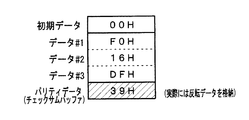
図31は、チェックサム作成方法の一例を説明するための説明図である。ただし、図31に示す例では、簡単のために、バックアップRAM領域のデータのサイズを3バイトとする。電源電圧低下にもとづく電力供給停止時処理において、図31に示すように、チェックサムデータとして初期データ(この例では00(H))が設定される。次に、「00(H)」と「F0(H)」の排他的論理和がとられ、その結果と「16(H)」の排他的論理和がとられる。さらに、その結果と「DF(H)」の排他的論理和がとられる。そして、その結果(この例では「39(H)」)を論理反転して得られた値(この例では「C6(H)」)がチェックサムバッファに設定される。
【0221】
なお、図31では、説明を容易にするために、論理反転前のデータ「39(H)」がチェックサムバッファに格納されている様子が示されている。なお、初期データとしての00(H)はステップS460で設定されるチェックサムデータに対するクリアデータに応じた値であるが、実際には、00(H)との排他的論理和は演算前と後とで値が変わらないので、00(H)との排他的論理和演算を行わなくてもよい。
【0222】
この実施の形態では、チェックサムバッファは、バックアップRAM領域(変動データ記憶手段)の最後のアドレスに格納されている。従って、例えば、チェックサム作成方法のプログラムに誤りがないかどうか確認する際に、容易にその確認を行うことができる。RAM領域の最終アドレスの値が正しいか否か確認すればよいからである。また、この実施の形態では、チェックサム算出開始アドレスはバックアップフラグが設定されるアドレスであり、チェックサム算出最終アドレスは賞球制御用フラグ・バッファのうちの最後のアドレスである(図30参照)。従って、賞球制御用フラグ・バッファの後、すなわち、バックアップRAM領域の最後のアドレスをチェックサムバッファの領域にすれば、RAM領域において無駄が生ずることはない。
【0223】
なお、確認のしやすさやRAM領域の無駄防止を考慮すると、バックアップRAM領域の最初のアドレスをチェックサムバッファの領域にしてもよい。
【0224】
また、遊技機への電力供給開始時にはパリティチェックOKか否かの判断が行われるが(図18におけるステップS10)、その判断では、電力供給停止時処理におけるパリティデータの作成処理(ステップS460〜S469)と同様の処理が行われ、処理結果すなわち演算結果がチェックサムバッファの内容と一致したらパリティチェックOKと判定される。
【0225】
なお、ここでは、バックアップRAM領域の最後または最初のアドレスをチェックサムバッファの領域にしたが、バックアップRAM領域の中途の領域にチェックサムバッファの領域を割り当ててもよい。また、この実施の形態では、作業領域のデータにもとづいてチェックサムが生成されているが、スタック領域のデータも含めてチェックサムを生成するようにしてもよい。
【0226】
さらに、この実施の形態では、電力供給開始時に、電力供給停止時処理における処理と同じ処理によってチェックサムを生成し、生成されたチェックサムとバックアップRAMに保存されていたチェックサムとを比較したが、他の方法を用いてもよい。例えば、バックアップRAMに保存されていたチェックサムを初期値として、電力供給停止時処理において演算対象となった各データについて演算を行い、演算結果が所定値(例えば00(H))と一致したらパリティチェックOKと判定するようにしてもよい。
【0227】
また、チェックのためのチェックデータはチェックサムに限られず、バックアップRAMの内容が正当に保存されているかを判定できるものであれば、他のチェックデータを用いてもよいし、チェックデータは複数あってもよい。その場合、各チェックデータのチェック対象となるRAM領域が別であってもよい。すなわち、RAM領域における複数部分の各部分についてチェックデータを作成するようにしてもよい。
【0228】
図32は、払出制御用CPU371周りの一構成例を示すブロック図である。図32に示すように、電源基板910の電源監視回路(電源監視手段)からの電源断信号が、バッファ回路960を介して払出制御用CPU371のマスク不能割込端子(XNMI端子)に接続されている。従って、払出制御用CPU371は、マスク不能割込処理によって遊技機への電力供給停止の発生を確認することができる。なお、バッファ回路960から出力される信号は電源監視回路910からの検出信号と実質的に変わらないので(増幅を受けたのみ)、以下、バッファ回路960から出力される信号を検出信号またはNMI信号と呼ぶことがある。
【0229】
払出制御用CPU371のCLK/TRG2端子には、主基板31からの払出制御用の割込信号が接続されている。CLK/TRG2端子にクロック信号が入力されると、払出制御用CPU371に内蔵されているタイマカウンタレジスタCLK/TRG2の値がダウンカウントされる。そして、レジスタ値が0になると割込が発生する。従って、タイマカウンタレジスタCLK/TRG2の初期値を「1」に設定しておけば、割込信号の入力に応じて割込が発生することになる。そして、払出制御用CPU371は、割込が発生すると、コマンド受信割込処理を実行する。
【0230】
払出制御基板37には、システムリセット回路975も搭載されているが、この実施の形態では、システムリセット回路975におけるリセットIC976は、電源投入時に、外付けのコンデンサに容量で決まる所定時間だけ出力をローレベルとし、所定時間が経過すると出力をハイレベルにする。また、リセットIC976は、VSLの電源電圧を監視して電圧値が所定値(例えば+9V)以下になると出力をローレベルにする。従って、遊技機への電力供給停止時には、リセットIC976からの信号がローレベルになることによって払出制御用CPU371がシステムリセットされる。
【0231】
リセットIC976が電力供給停止を検知するための所定値は、通常時の電圧より低いが、払出制御用CPU371が暫くの間動作しうる程度の電圧である。また、リセットIC976が、払出制御用CPU371が必要とする電圧(この例では+5V)よりも高い電圧を監視するように構成されているので、払出制御用CPU371が必要とする電圧に対して監視範囲を広げることができる。従って、より精密な監視を行うことができる。
【0232】
+5V電源から電力が供給されていない間、払出制御用CPU371の内蔵RAMの少なくとも一部は、電源基板から供給されるバックアップ電源がバックアップ端子に接続されることによってバックアップされ、停電等の遊技機に対する電力供給停止が発生しても内容は保存される。そして、+5V電源が復旧すると、システムリセット回路975からリセット信号が発せられるので、払出制御用CPU371は、通常の動作状態に復旧する。そのとき、必要なデータがバックアップされているので、停電等からの復旧時には停電発生時の払出制御状態に復旧させることができる。
【0233】
なお、図32に示された構成では、システムリセット回路975は、電源投入時に、コンデンサの容量で決まる期間のローレベルを出力し、その後ハイレベルを出力する。すなわち、リセット解除タイミングは1回だけである。しかし、図9に示された主基板31の場合と同様に、複数回のリセット解除タイミングが発生するような回路構成を用いてもよい。
【0234】
また、図32に示す例では、リセットIC976のCK端子には払出制御用CPU371の出力ポートから、ある時間間隔で信号が供給される。その信号が途絶えて所定期間(ウォッチドッグタイマのタイムアウト時間)以上信号の入力がない状態になると、リセットIC976は、リセット信号のレベルを一旦リセットレベルにする。図32では、払出制御用CPU371からリセットIC976に対する信号は内蔵出力ポートから出力される例が示されているが、その信号は、外付けの出力ポートから出力されるようにしてもよい。
【0235】
また、払出制御用CPU371がウォッチドッグ機能を内蔵しウォッチドッグタイマのタイムアウトによって内部的に払出制御用CPU371にリセットがかかるようなCPUであり、その機能を利用している場合には、リセットIC976のCK端子に信号を与えるような構成を用いなくてもよい。
【0236】
図33は、この実施の形態における出力ポートの割り当てを示す説明図である。図33に示すように、出力ポートC(アドレス00H)は、払出モータ289に出力される駆動信号等の出力ポートである。また、出力ポートD(アドレス01H)は、7セグメントLEDであるエラー表示LED374に出力される表示制御信号の出力ポートである。そして、出力ポートE(アドレス02H)は、振分ソレノイド310に出力される駆動信号、およびカードユニット50に対するEXS信号とPRDY信号とを出力するための出力ポートである。
【0237】
図34は、この実施の形態における入力ポートのビット割り当てを示す説明図である。図34に示すように、入力ポートA(アドレス06H)は、主基板31から送出された払出制御コマンドの8ビットの払出制御信号を取り込むための入力ポートである。また、入力ポートB(アドレス07H)のビット0〜1には、それぞれ、賞球カウントスイッチ301Aおよび球貸しカウントスイッチ301Bの検出信号が入力される。ビット2〜5には、カードユニット50からのBRDY信号、BRQ信号、VL信号およびクリアスイッチ921の検出信号が入力される。また、ビット7には、主基板31からの払出制御信号用STB信号が入力される。
【0238】
なお、図12に示すように、この実施の形態では、出力ポートおよび入力ポートとして、外付けのものが使用されているが、払出制御用CPU371に内蔵されているPIOを用いてもよい。
【0239】
図35は、払出制御手段(払出制御用CPU371およびROM,RAM等の周辺回路)がプログラムに従って実行するメイン処理を示すフローチャートである。メイン処理では、払出制御用CPU371は、まず、必要な初期設定を行う。すなわち、払出制御用CPU371は、まず、割込禁止に設定する(ステップS700)。次に、割込モードを割込モード2に設定し(ステップS701)、スタックポインタにスタックポインタ指定アドレスを設定する(ステップS702)。また、払出制御用CPU371は、内蔵デバイスレジスタの初期化を行い(ステップS703)、CTCおよびPIOの初期化(ステップS704)を行った後に、ウォッチドッグクリア処理(ステップS705)を行って、RAMをアクセス可能状態に設定する(ステップS706)。ステップS6では、払出制御用CPU371がウォッチドッグ機能を内蔵し、それを利用している場合には、ウォッチドッグ機能の初期化およびタイマクリア処理が行われる。
【0240】
この実施の形態では、内蔵CTCのうちの一つのチャネルがタイマモードで使用される。従って、ステップS703の内蔵デバイスレジスタの設定処理およびステップS704の処理において、使用するチャネルをタイマモードに設定するためのレジスタ設定、割込発生を許可するためのレジスタ設定および割込ベクタを設定するためのレジスタ設定が行われる。そして、そのチャネルによる割込がタイマ割込として用いられる。タイマ割込を例えば1ms毎に発生させたい場合は、初期値として1msに相当する値が所定のレジスタ(時間定数レジスタ)に設定される。
【0241】
なお、タイマモードに設定されたチャネル(この実施の形態ではチャネル3)に設定される割込ベクタは、タイマ割込処理の先頭アドレスに相当するものである。具体的は、Iレジスタに設定された値と割込ベクタとでタイマ割込処理の先頭アドレスが特定される。タイマ割込処理では、払出制御処理が実行される。
【0242】
また、内蔵CTCのうちの他の一つのチャネル(この実施の形態ではチャネル2)が、遊技制御手段からの払出制御コマンド受信のための割込発生用のチャネルとして用いられ、そのチャネルがカウンタモードで使用される。従って、ステップS703の内蔵デバイスレジスタの設定処理およびステップS704の処理において、使用するチャネルをカウンタモードに設定するためのレジスタ設定、割込発生を許可するためのレジスタ設定および割込ベクタを設定するためのレジスタ設定が行われる。
【0243】
カウンタモードに設定されたチャネル(チャネル2)に設定される割込ベクタは、後述するコマンド受信割込処理の先頭アドレスに相当するものである。具体的は、Iレジスタに設定された値と割込ベクタとでコマンド受信割込処理の先頭アドレスが特定される。
【0244】
この実施の形態では、払出制御用CPU371でも割込モード2が設定される。従って、内蔵CTCのカウントアップにもとづく割込処理を使用することができる。また、CTCが送出した割込ベクタに応じた割込処理開始アドレスを設定することができる。
【0245】
CTCのチャネル2(CH2)のカウントアップにもとづく割込は、上述したタイマカウンタレジスタCLK/TRG2の値が「0」になったときに発生する割込である。従って、例えばステップS705において、特定レジスタとしてのタイマカウンタレジスタCLK/TRG2に初期値「1」が設定される。さらに、CLK/TRG2端子に入力される信号の立ち上がりまたは立ち下がりで特定レジスタとしてのタイマカウンタレジスタCLK/TRG2のカウント値が−1されるのであるが、所定の特定レジスタの設定によって、立ち上がり/立ち下がりの選択を行うことができる。この実施の形態では、CLK/TRG2端子に入力される信号の立ち上がりで、タイマカウンタレジスタCLK/TRG2のカウント値が−1されるような設定が行われる。
【0246】
また、CTCのチャネル3(CH3)のカウントアップにもとづく割込は、CPUの内部クロック(システムクロック)をカウントダウンしてレジスタ値が「0」になったら発生する割込であり、後述する1msタイマ割込として用いられる。具体的には、CPU371の動作クロックを分周したクロックがCTCに与えられ、クロックの入力によってレジスタの値が減算され、レジスタの値が0になるとタイマ割込が発生する。例えば、CH3のレジスタ値はシステムクロックの1/256周期で減算される。分周したクロックにもとづいて減算が行われるので、レジスタの初期値は大きくならない。ステップS705において、CH3のレジスタには、初期値として1msに相当する値が設定される。
【0247】
CTCのCH2のカウントアップにもとづく割込は、CH3のカウントアップにもとづく割込よりも優先順位が高い。従って、同時にカウントアップが生じた場合に、CH2のカウントアップにもとづく割込、すなわち、コマンド受信割込処理の実行契機となる割込の方が優先される。
【0248】
次いで、払出制御用CPU371は、入力ポートB(図34参照)を介して入力されるクリアスイッチ921の出力信号の状態を1回だけ確認する(ステップS707)。その確認においてオンを検出した場合には、払出制御用CPU371は、通常の初期化処理を実行する(ステップS711〜ステップS713)。クリアスイッチ921がオンである場合(押下されている場合)には、ローレベルのクリアスイッチ信号が出力されている。なお、入力ポート372では、クリアスイッチ信号のオン状態はハイレベルである。
【0249】
なお、払出制御用CPU371は、例えば、オン状態が少なくとも1ms(1ms毎に起動される処理の1回目の処理における検出直前に検出信号がオンした場合)継続しないとスイッチオンとは見なさないが、クリアスイッチ921のオン検出の場合には、1回のオン判定でオン/オフが判定される。すなわち、初期化操作手段としてのクリアスイッチ921が所定の操作状態であるか否かを払出制御用CPU371が判定するための初期化要求検出判定期間は、遊技媒体検出手段としての賞球カウントスイッチ等が遊技媒体を検出したことを判定するための遊技媒体検出判定期間とは異なる期間とされている。
【0250】
クリアスイッチ921がオンの状態でない場合には、払出制御用CPU371は、払出制御用のバックアップRAM領域にバックアップデータが存在しているか否かの確認を行う(ステップS708)。例えば、主基板31のCPU56の処理と同様に、遊技機への電力供給停止時にセットされるバックアップフラグがセット状態になっているか否かによって、バックアップデータが存在しているか否か確認する。バックアップフラグがセット状態になっている場合には、バックアップデータありと判断する。
【0251】
バックアップありを確認したら、払出制御用CPU371は、バックアップRAM領域のデータチェック(この例ではパリティチェック)を行う。不測の停電等の電力供給の停止が生じた後に復旧した場合には、バックアップRAM領域のデータは保存されていたはずであるから、チェック結果は正常になる。チェック結果が正常でない場合には、内部状態を電力供給の停止時の状態に戻すことができないので、不測の停電等からの復旧時ではなく電源投入時に実行される初期化処理を実行する。
【0252】
チェック結果が正常であれば(ステップS709)、払出制御用CPU371は、内部状態を電力供給停止時の状態に戻すための払出状態復旧処理を行う(ステップS710)。そして、バックアップRAM領域に保存されていたPC(プログラムカウンタ)の指すアドレスに復帰する。
【0253】
バックアップフラグとチェックサム等のチェックデータとを用いてバックアップRAM領域のデータが保存されているか否かを確認することによって、払出制御状態を電力供給停止時の状態に正確に戻すことができる。すなわち、バックアップRAM領域のデータにもとづく状態復旧処理の確実性が向上する。なお、この実施の形態では、バックアップフラグとチェックデータとの双方を用いてバックアップRAM領域のデータが保存されているか否かを確認しているが、いずれか一方のみを用いてもよい。すなわち、バックアップフラグとチェックデータとのいずれかを、状態復旧処理を実行するための契機としてもよい。
【0254】
このように、遊技制御手段以外の電気部品制御手段においても、電力供給が開始された場合に、電力供給が停止する前の制御状態に復旧させるか否かを決めるための復旧条件が複数あり、電気部品制御手段は、復旧条件の全てが成立していたら電力供給が停止する前の制御状態に復旧させ、復旧条件のうち少なくとも1つが成立していなかったら制御状態を初期化する初期化処理を行うように構成されている。従って、誤って復旧処理がなされ、誤った制御がなされてしまうことが防止される。なお、この例では、復旧条件の成立は、クリアスイッチ921の押下がないこと、バックアップフラグがオン状態であること、およびパリティチェックの結果が正常であったことである。
【0255】
この実施の形態では、電力供給停止時処理を実行したことを示すフラグとして1バイトデータであるバックアップフラグを用いたが、電力供給停止時処理を実行したことを示すフラグであればどのような形態のフラグを用いてもよい。また、そのようなフラグは複数あってもよい。
【0256】
初期化処理では、払出制御用CPU371は、まず、RAMクリア処理を行う(ステップS711)。ここでは、RAMの全領域をクリアする。そして、1ms毎に定期的にタイマ割込がかかるように払出制御用CPU371に設けられているCTCのレジスタの設定が行われる(ステップS712)。すなわち、初期値として1msに相当する値が所定のレジスタ(時間定数レジスタ)に設定される。そして、初期設定処理のステップS701において割込禁止とされているので、初期化処理を終える前に割込が許可される(ステップS713)。
【0257】
次いで、払出制御処理(ステップS751〜S760)が繰り返し(ループ処理で)実行される。
【0258】
払出制御処理において、払出制御用CPU371は、まず、ウォッチドッグクリア処理を実行する(ステップS751)。ステップS751では、払出制御用CPU371がウォッチドッグ機能を内蔵し、それを利用している場合には、内蔵されているウォッチドッグタイマにタイマクリアするためのデータを書き込む処理が行われる。また、図34に例示したように、リセットIC976に信号を与えることによってウォッチドッグ機能を実現している場合には、1パルスの信号を出力する。
【0259】
また、入力ポート372bに入力される賞球カウントスイッチ301Aや球貸しカウントスイッチ301B等のスイッチがオンしたか否かを判定する(スイッチ処理:ステップS752)。ただし、この実施の形態では、後述するように、タイマ割込処理において、入力ポートのデータが所定のRAM領域に保存されている。ステップS752のスイッチ処理では、そのRAM領域を介して、賞球カウントスイッチ301Aや球貸しカウントスイッチ301B等のスイッチの検出信号を認識し、それらの状態判定を行う。
【0260】
次に、払出制御用CPU371は、主基板31から払出停止状態指定コマンドを受信していたら払出停止状態に設定し、払出可能状態指定コマンドを受信していたら払出停止状態の解除を行う(払出停止状態設定処理:ステップS753)。また、受信した払出制御コマンドを解析し、解析結果に応じた処理を実行する(コマンド解析実行処理:ステップS754)。さらに、プリペイドカードユニット制御処理を行う(ステップS755)。
【0261】
次いで、払出制御用CPU371は、球貸し要求に応じて貸し球を払い出す制御を行う(ステップS756)。このとき、払出制御用CPU371は、振分ソレノイド310によって球振分部材311を球貸し側に設定する。
【0262】
さらに、払出制御用CPU371は、総合個数記憶に格納された個数の賞球を払い出す賞球制御処理を行う(ステップS757)。このとき、払出制御用CPU371は、振分ソレノイド310によって球振分部材311を賞球側に設定する。そして、出力ポート372cおよび中継基板72を介して球払出装置97の払出機構部分における払出モータ289に対して駆動信号を出力し、所定の回転数分払出モータ289を回転させる払出モータ制御処理を行う(ステップS758)。ただし、この実施の形態では、後述するように、遊技制御手段の場合と同様に、タイマ割込処理において、出力ポート出力内容記憶領域のデータが出力ポートに出力される。従って、払出モータ制御処理では、出力ポート出力内容記憶領域に駆動信号等を設定する。
【0263】
なお、この実施の形態では、払出モータ289としてステッピングモータが用いられ、それらを制御するために1−2相励磁方式が用いられる。従って、具体的には、払出モータ制御処理において、8種類の励磁パターンデータが繰り返し払出モータ289に出力される。また、この実施の形態では、各励磁パターンデータが4msずつ出力される。
【0264】
次いで、エラー検出処理が行われ、その結果に応じてエラー表示LED374に所定の表示を行う(エラー処理:ステップS759)。また、遊技機外部に出力される球貸し個数信号を出力する処理等を行う(出力処理:ステップS760)。その後、ステップS751に戻る。
【0265】
図36は、ステップS710の払出状態復旧処理の一例を示すフローチャートである。払出状態復旧処理において、払出制御用CPU371は、まず、スタックポインタの復旧処理を行う(ステップS731)。スタックポインタの値は、後述する電力供給停止時処理において、所定のRAMエリア(電源バックアップされている)に退避している。よって、ステップS731では、そのRAMエリアの値をスタックポインタに設定することによって復旧させる。なお、復旧されたスタックポインタが指す領域(すなわちスタック領域)には、電力供給が停止したときのレジスタ値やプログラムカウンタ(PC)の値が退避している。
【0266】
そして、CTCやPIOなどの内蔵デバイスの初期設定を行い、また、スタック領域から各種レジスタの退避値を読み出して、各種レジスタに設定する(ステップS732)。すなわち、レジスタ復元処理を行う。ここで、RAMアクセス許可状態に設定する処理も行う。さらに、バックアップフラグをクリアする(ステップS733)。すなわち、前回の電力供給停止時に所定の記憶保護処理が実行されたことを示すフラグをリセットする。そして、パリティフラグがオンしていない場合には割込許可状態にする(ステップS734,S735)。最後に、内部状態を払出禁止状態に設定して(ステップS736)、AFレジスタ(アキュミュレータとフラグのレジスタ)をスタック領域から復元する(ステップS737)。なお、内部状態を払出禁止状態に設定するということは、例えば、対応する内部フラグを設定することである。また、通常の電力供給開始時(払出状態復旧処理が行われない場合)にも、内部状態を払出禁止状態に設定する。そして、主基板31の遊技制御手段は、起動時に、払出ができる状態(例えば球切れスイッチ187がオン状態でなく下皿満タン状態でもない状態)にあるか否かを判断し、払出ができる状態であれば、払出可能状態を示す払出制御コマンドを送信する。そのような払出制御コマンドの受信に応じて、払出制御手段は、払出禁止状態を解除する。このような制御によって、払出制御手段が、払出を開始させるべきでないにも関わらず球払出装置97に球払出を開始させてしまうことが防止される。
【0267】
そして、RET命令が実行されるのであるが、ここでのリターン先は、払出状態復旧処理をコールした部分ではない。なぜなら、ステップS731においてスタックポインタの復旧処理がなされ、復旧されたスタックポインタが指すスタック領域に格納されているリターンアドレスは、プログラムにおける前回の電力供給停止時にNMIが発生したアドレスである。従って、ステップS736の次のRET命令によって、電力供給停止時にNMIが発生したアドレスにリターンする。すなわち、スタック領域に退避されていたアドレスにもとづいて復旧制御が実行されている。
【0268】
図37は、タイマ割込処理を示すフローチャートである。タイマ割込処理において、払出制御用CPU371は、レジスタの退避処理を行った後(ステップS761)、ポート入力処理(ステップS762)、ポート出力処理(ステップS763)およびタイマ更新処理(ステップS764)を行う。そして、レジスタの復旧処理を行い(ステップS765)、割込許可状態にして(ステップS766)、処理を終了する。
【0269】
ステップS762のポート入力処理は、入力ポートのデータを読み出して、読み出したデータを所定のRAM領域に書き込む処理である。払出制御処理(図35に示されたループ処理)では、RAM領域の内容にもとづいて入力ポートの入力状態を認識する。ステップS763のポート出力処理は、出力ポート出力内容記憶領域の内容を対応する出力ポートに出力する処理である。ステップS764のタイマ更新処理は、払出制御処理において用いられている各種タイマの値を減算する処理である。例えば、払出制御処理では、タイマに計測時間に相当した値をタイマにセットし、タイマの値が0になったらタイムアウトしたと認識する。
【0270】
図38は、この実施の形態におけるRAM領域のアドレスマップを示す説明図である。図38に示すように、RAM領域の先頭はバックアップフラグの領域に割り当てられている。そして、最後部にチェックサムバッファの領域が割り当てられている。なお、バックアップフラグからチェックサムバッファまでの領域は作業領域に相当し、チェックサムバッファ以降の領域にスタック領域が設定されている。また、この実施の形態では、RAM領域の全てが電源バックアップされている。
【0271】
図38に示すように、保護領域には、総賞球数バッファ、貸し球個数記憶、払出状態フラグ等が設定されている。総賞球数バッファは、主基板31の側から指示された賞球払出個数(賞球数)の総数を記憶するものである。貸し球個数記憶は、未払出の球貸し個数を記憶するものである。払出状態フラグは、払出可能状態にあるのか払出禁止状態にあるのかを示すフラグである。保護領域以外の領域は、その内容が保存されていなくても制御状態を復旧させることができるようなデータを記憶する領域であり、一時的発生するデータを保存するワークエリア等である。なお、この実施の形態では、保護領域およびその他の領域は、払出制御復旧処理においてクリアされない。
【0272】
図39は、主基板31からの割込信号(払出制御用)に応じて起動されるコマンド受信割込処理を示すフローチャートである。コマンド受信割込処理において、払出制御用CPU371は、レジスタの退避処理を行った後(ステップS771)、入力ポートB(図34参照)のデータを入力する(ステップS772)。そして、そのビット7(払出制御用STB信号)を確認する(ステップS773)。払出制御用STB信号がオン状態であれば、入力ポートA(図34参照)のデータを入力する(ステップS774)。そして、入力したデータを、コマンド受信個数カウンタが示す受信コマンドバッファに格納し(ステップS775)、コマンド受信個数カウンタの値を更新する(ステップS776)。
【0273】
その後、レジスタ復旧処理を行い(ステップS777)、割込許可状態にして(ステップS778)、処理を終了する。以上のように、この実施の形態では、払出制御手段は、指示信号(割込信号)とデータ出力中信号(STB信号)の両方の出力を検出した場合に、コマンドデータを入力する処理(ステップS774)を実行することになる。
【0274】
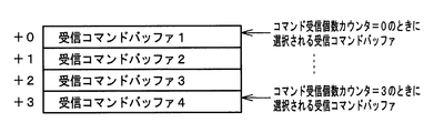
図40は、主基板31から受信した払出制御コマンドを格納するための受信バッファの一構成例を示す説明図である。この例では、払出制御コマンドを4個格納可能なリングバッファ形式の受信バッファが用いられる。従って、受信バッファは、受信コマンドバッファ1〜4の4バイトの領域で構成される。そして、受信したコマンドをどの領域に格納するのかを示すコマンド受信個数カウンタが用いられる。コマンド受信個数カウンタは、0〜3の値をとる。
【0275】
なお、コマンド解析実行処理は図35に示されたメイン処理で実行され、その処理において、読出ポインタが指す受信バッファの内容が読み出されるとともに読出ポインタの値が+1される。また、主基板31の遊技制御手段は、4msの制御期間において1つしか払出制御コマンドを送信しない。従って、通常、受信バッファに、複数の払出制御コマンドが記憶されていることはない。
【0276】
図41および図42は、電源基板910からの電源断信号に応じて実行されるマスク不能割込処理(NMI処理:電力供給停止時処理)の処理例を示すフローチャートである。
【0277】
電力供給停止時処理において、払出制御用CPU371は、AFレジスタを所定のバックアップRAM領域に退避する(ステップS801)。また、割込フラグをパリティフラグにコピーする(ステップS802)。パリティフラグはバックアップRAM領域に形成されている。割込フラグは、割込許可状態であるのか割込禁止状態であるのかを示すフラグであって、払出制御用CPU371が内蔵する制御レジスタ中にある。割込フラグのオン状態が割込禁止状態であることを示す。上述したように、パリティフラグは遊技状態復旧処理で参照される。そして、払出状態復旧処理において、パリティフラグがオン状態であれば、割込許可状態には設定されない。
【0278】
また、BCレジスタ、DEレジスタ、HLレジスタおよびIXレジスタをバックアップRAM領域に退避する(ステップS804〜807)。なお、ステップS801〜S807の処理は、電源監視手段の検出信号に応じて制御状態を復旧させるために必要なデータを変動データ記憶手段に保存させるためのデータ退避処理に相当する。
【0279】
次に、処理ループ回数としてあらかじめ決められた値をセットし(ステップS808)、賞球カウントスイッチ301Aのチェック処理と払出制御コマンド受信処理とを所定期間実行するループ処理に移行する。払出制御用CPU371は、まず、ウォッチドッグクリア処理を行う(ステップS810)。次いで、入力ポートB(図34参照)のデータを入力する(ステップS811)。そして、入力したデータのビット7(払出制御用STB信号)を確認する(ステップS812)。払出制御用STB信号がオン状態であって、オン状態の確認が最初のものであれば(ステップS813)、入力ポートA(図34参照)のデータを入力し、入力したデータをコマンドバッファに格納する(ステップS814)。
【0280】
コマンドバッファは、通常の制御時に使用される通常時コマンド記憶領域としての受信バッファ(図40参照)とは異なるRAM領域に設けられているバックアップコマンド記憶領域であり、電力供給停止時でも所定期間は保存される。
【0281】
次いで、ポートチェック回数としてあらかじめ決められている値をセットし(ステップS815)、入力ポートB(図34参照)のデータを入力する(ステップS816)。そして、スイッチチェックタイミングが到来していない場合には(ステップS817)、ポートチェック回数を減算し(ステップS818)、その値が0になっていなければステップS816に戻る(ステップS819)。0になっていれば、ステップS823に移行する。
【0282】
スイッチチェックタイミングが到来している場合には、スイッチチェック処理を行い(ステップS820)、賞球カウントスイッチ301Aがオンしたことを検出したら(ステップS821)、総賞球数バッファの値を減算し(ステップS821)、ステップS823に移行する。なお、スイッチチェック処理は、賞球カウントスイッチ301Aが確かにオンしたか否かを検出する処理であり、例えば、所定回連続してオン状態が検出されたら、ステップS821で賞球カウントスイッチ301Aが確かにオンしたと判断される。
【0283】
ステップS823では、処理ループ回数を減算し、処理ループ回数が0になっていなければステップS810に戻る(ステップS824)。処理ループ回数が0になっていれば、ステップS831に移行する。
【0284】
ステップS831ではスタックポインタをバックアップRAM領域に退避させ、さらに、バックアップあり指定値(この例では「55(H)」)をバックアップフラグにストアする。バックアップフラグはバックアップRAM領域に形成されている。次いで、主基板31のCPU56の処理と同様の処理を行ってパリティデータを作成しバックアップRAM領域に保存する(ステップS833〜S842)。そして、RAMアクセスレジスタにアクセス禁止値を設定する(ステップS843)。以後、内蔵RAMのアクセスができなくなる。
【0285】
その後、払出制御用CPU371は、待機状態(ループ状態)に入る。従って、システムリセットされるまで、何もしない状態になる。なお、ウォッチドッグタイマを使用している場合には、ループ状態でウォッチドッグクリア処理を行っていないので、ウォッチドッグタイマがタイムアウトする。ただし、正常な電力供給停止時にはその前にシステムリセットがかかる。しかし、例えばノイズ等によってNMIがかかった場合には、電力供給停止時ではないのでシステムリセットがかからないが、ウォッチドッグタイマのタイムアウトによってリセットがかかり、ループから抜け出すことができる。
【0286】
図23に示されたb〜e期間において電力供給が停止しマスク不能割込が主基板31のCPU56にかかると、CPU56は、出力ポートの出力状態を変更しないので、払出制御用STB信号が出力されていた場合にはその出力状態は維持されている。すなわち、遊技制御手段は、コマンドデータの出力に関連してコマンドデータを出力していることを示すデータ出力中信号(この例ではSTB信号)を出力するとともに、電力供給停止時処理を開始した後にも所定期間(上記の例ではシステムリセットされるまでであって、払出制御手段がコマンド受信を完了するまでの期間よりも短い期間)はデータ出力中信号の出力を維持している。電力供給が停止するときには払出制御用CPU371にもマスク不能割込がかかるが、払出制御用CPU371が実行するマスク不能割込処理において、所定期間(この例では処理ループ回数の初期値×S810〜S824のループ時間)データ出力中信号の状態を監視し(ステップS812)、データ出力中信号が出力されている場合には、コマンドデータを取り込む処理を実行する。そして、コマンドデータが受信されコマンドバッファに格納される(ステップS814)。従って、b〜e期間において電力供給が停止する場合には、払出制御手段において、送信途中であった払出制御コマンドの受信が完了する。
【0287】
なお、図23に示されたc〜d期間において電力供給が停止しマスク不能割込が主基板31のCPU56にかかると、電力供給停止のタイミングによっては、電力供給再開後の払出状態復旧処理によってコマンド受信割込処理に復旧し、コマンド受信割込処理によって払出制御コマンドを受信してしまう場合も考えられる。
【0288】
そこで、この実施の形態では、メイン処理におけるコマンド解析実行処理(ステップS754)において、まず、コマンドバッファにデータがあるか否か確認する。コマンドバッファは電力供給停止時処理において受信した払出制御コマンドを格納するバックアップコマンド記憶領域であり、電力供給停止時でも所定期間は保存されている。コマンドバッファにデータがある場合には、そのデータについてコマンド解析処理を実行した後、コマンドバッファの内容をクリアするとともに、さらに、通常時コマンド記憶領域としての受信バッファをクリアする。すなわち、通常時コマンド記憶領域の内容を無効にする。
【0289】
なお、コマンド解析処理は受信されていた払出制御コマンドがいかなるコマンドであるかを解析する処理であり、例えば、賞球個数を指示する払出制御コマンドであったことが確認されたら、後述する総賞球数バッファの内容を更新する。そして、コマンド受信カウンタを初期化する。すなわち、読出ポインタの値と一致させる。
【0290】
メイン処理において、このような制御を行えば、電力供給が停止するときにコマンド受信割込処理の処理途中であって、電力供給が復旧してコマンド割込処理の実行が再開され、受信コマンドを受信バッファに格納したとしても、その受信コマンドはメイン処理において破棄される。よって、払出制御コマンドがコマンドバッファと受信バッファの双方に格納されるという状況、すなわち、払出制御コマンドを二重に受信してしまうという状況が発生することはない。なお、上述したように、コマンド受信割込処理中に停電等の不測の電力供給停止が発生した場合、本来コマンド受信割込処理によって受信されるべき払出制御コマンドは、電力供給停止時処理によって受信され、コマンドバッファに格納されている。
【0291】
実施の形態2.
図43は、第2の実施の形態(実施の形態2)における主基板31から各電気部品制御基板(サブ基板)に送信される制御コマンド(払出制御コマンド、表示制御コマンド、ランプ制御コマンド、音制御コマンド)の送出形態を示すタイミング図である。この例では、制御コマンドのコマンドデータは1バイトで構成されている。
【0292】
図43に示すように、主基板31(メイン)から割込信号がオン状態になった後オフ状態になったら、コマンドデータが出力される。さらに、STB信号がオン状態になる。このように、遊技制御手段は、電気部品制御手段がコマンドデータを入力する入力処理を実行する契機を示す信号(この例では割込信号)を送信した後、コマンドデータを出力し、コマンドデータを出力した後に、入力処理実行中における実際の入力の契機を示す信号として指示信号(この例ではSTB信号)を出力する。サブ基板では、電気部品制御手段を構成するマイクロコンピュータに対して割込信号の立ち上がりで割込がかかり、制御コマンドの受信処理(入力処理)が開始される。
【0293】
サブ基板の電気部品制御手段は、受信処理において、STB信号がオン状態になったらコマンドデータを取り込む。その後、サブ基板の電気部品制御手段がコマンド受信処理を完了した後のタイミングで、メインからのSTB信号はオフ状態になる。
【0294】
この実施の形態でも、遊技制御手段は、制御コマンドの送出処理を除いて、実施の形態1の場合と同様な制御を行う。すなわち、電源断信号に応じて電力供給停止時処理を実行する(図29参照)。また、電力供給開始時に、復旧条件が成立していることを確認したら、遊技状態復旧処理を行う。遊技状態復旧処理において、保存されていた出力ポート0〜4出力内容記憶領域の内容を出力ポート0〜4に出力する処理を行う(図28のステップS96参照)。なお、この実施の形態でも、入出力ポートの信号割り当ては、実施の形態1の場合と同じである。
【0295】
図44は、この実施の形態における遊技制御手段のタイマ割込処理(図26参照)で実行されるポート出力処理(ステップS102)の構成例を示すフローチャートである。ポート出力処理において、CPU56は、出力ポート5出力内容記憶領域のデータを出力ポート5(図16参照)に出力する(ステップS371)。また、出力ポート6出力内容記憶領域のデータを出力ポート6(図16参照)に出力する(ステップS372)。なお、出力ポート5出力内容記憶領域および、出力ポート6出力内容記憶領域には、遊技制御処理(図19に示されたループ処理)において、出力ポートの各ビットのオン/オフに応じたデータが設定されている。
【0296】
次いで、CPU56は、制御コマンド(払出制御コマンド、表示制御コマンド、ランプ制御コマンド、音制御コマンド)を送信するための制御(ステップS373〜S386)を行う。まず、制御コマンド送出要求フラグ(払出制御コマンド送出要求フラグ、表示制御コマンド送出要求フラグ、ランプ制御コマンド送出要求フラグまたは音制御コマンド送出要求フラグ)がセットされているか否か確認する(ステップS373)。いずれの制御コマンド送出要求フラグもセットされていない場合には、何もせずリターンする。
【0297】
いずれかの制御コマンド送出要求フラグがセットされている場合には、コマンドデータを出力する出力ポート0の割込信号のビット(ビット0〜3のいずれか)に「1」を出力する(ステップS374)。例えば、払出制御コマンドを送信する場合には、出力ポート0のビット0(払出制御信号用割込信号)に「1」を出力する。また、制御コマンド送出要求フラグをリセットしておく(ステップS375)。さらに、出力ポート0の出力状態を出力ポート0出力内容記憶領域にコピーしておく(ステップS376)。このタイミングは、図43におけるa区間の開始時に相当する。
【0298】
次に、CPU56は、図43におけるa区間とb区間の時間の合計に相当する時間だけ待ってから(ステップS377)、コマンドデータを出力する出力ポート(出力ポート1〜出力ポート4のいずれか)に対応した出力ポート0の割込信号のビット(ビット0〜3のいずれか)を「0」にする(ステップS378)。例えば、払出制御コマンドを送信する場合には、出力ポート0のビット0(払出制御信号用割込信号)に「0」を出力する。さらに、出力ポート0の出力状態を出力ポート0出力内容記憶領域にコピーしておく(ステップS379)。このタイミングは、図43におけるc区間の開始時に相当する。なお、a区間は、主基板31が割込信号を出力してからサブ基板において割込が受け付けられるまでの遅れ時間に相当する。
【0299】
次いで、CPU56は、ステップS373で確認した制御コマンド送出要求フラグに対応したポート出力内容記憶領域(出力ポート1出力内容記憶領域〜出力ポート4出力内容記憶領域のいずれか)のデータを、対応する出力ポート(出力ポート1〜出力ポート4のいずれか)に出力する(ステップS380)。例えば、払出制御コマンド送出要求フラグがセットされていた場合には、出力ポート1出力内容記憶領域のデータを出力ポート1(図15参照)に出力する。
【0300】
なお、メイン処理ではポート出力内容記憶領域ではなくバックアップRAMにおける他の領域にコマンドデータを書き込み、実際にコマンドデータが出力ポートに出力されるときに、ポート出力内容記憶領域にコマンドデータを書き込むように構成した場合には、出力ポートにコマンドデータを出力するときに、ポート出力内容記憶領域に、出力ポートに出力したコマンドデータを設定する。また、なお、ステップS379とS380との間に、ディレイ時間をおいてもよい。
【0301】
次に、CPU56は、図43におけるd区間の時間に相当する時間だけ待ってから(ステップS381)、出力ポート0の、コマンドデータを出力した出力ポート(出力ポート1〜出力ポート4のいずれか)に対応した出力ポート0のSTB信号のビット(ビット4〜7のいずれか)に「1」を出力する(ステップS382)。例えば、ステップS380において出力ポート1出力内容記憶領域のデータを出力ポート1に出力した場合には、出力ポート0のビット4(払出制御信号用STB信号)に「1」を出力する。さらに、出力ポート0の出力状態を出力ポート0出力内容記憶領域にコピーしておく(ステップS383)。このタイミングは、図43におけるe区間の開始時に相当する。なお、ステップS381の処理を行わないようにしてもよい。また、サブ基板では、d区間開始のタイミングから、やや遅れて受信処理が開始される。その遅れは、サブ基板におけるマイクロコンピュータの処理遅れ(ソフトウェアがSTB信号のオンを検知するまでの遅れ)である。
【0302】
そして、CPU56は、図43におけるe区間の時間に相当する時間だけ待ってから(ステップS384)、出力ポート0の、コマンドデータを出力した出力ポート(出力ポート1〜出力ポート4のいずれか)に対応した出力ポート0のSTB信号のビット(ビット4〜7のいずれか)に「0」を出力する(ステップS385)。例えば、ステップS380において出力ポート1出力内容記憶領域のデータを出力ポート1に出力した場合には、出力ポート0のビット4(払出制御信号用STB信号)に「0」を出力する。さらに、出力ポート0の出力状態を出力ポート0出力内容記憶領域にコピーしておく(ステップS386)。このタイミングは、図43におけるe区間の終了時に相当する。
【0303】
なお、ステップS373において、制御コマンド送出要求フラグ(払出制御コマンド送出要求フラグ、表示制御コマンド送出要求フラグ、ランプ制御コマンド送出要求フラグまたは音制御コマンド送出要求フラグ)がリセット状態であった場合には、リセット状態であった制御コマンド送出要求フラグに対応したポート出力内容記憶領域(出力ポート1出力内容記憶領域〜出力ポート4出力内容記憶領域のいずれか)に、所定のデータ(例えばやFF(H)やクリアデータとしての00(H))を設定するとともに、対応する出力ポート(出力ポート1〜出力ポート4のいずれか)に、同じ値を出力するようにしてもよい。すなわち、制御期間(この例では1ms)内に制御コマンドの送出制御を実行しない場合には、ポート出力内容記憶領域の内容を所定内容としてもよい。所定のデータをFF(H)にした場合には、電力供給が復旧したときに、全てのポートのビットを監視していずれかがオン状態になるかどうかを判断するだけで容易にポートの状態が復旧したか否か確認することができる。つまり、変化の有無を確認する場合に比べて容易にポートの状態が復旧したか否か確認することができる。
【0304】
以上のようにして、図43に示されたようなタイミングで、制御コマンドがサブ基板に送出される。なお、タイマ割込がかかったときに、複数種類の制御コマンド送出要求フラグがオンしていたときには、例えば、あらかじめ決められている優先順位に従って、いずれかの制御コマンド送出要求フラグについてステップS374〜S386の処理が実行される。
【0305】
このように、この実施の形態では、制御コマンドのコマンドデータを出力するときに、ポート出力内容記憶領域のデータを出力ポートに出力する。そして、ポート出力内容記憶領域のデータは、電力供給が停止しても所定期間はその内容が保存されるバックアップRAMに設定される。上述したように、メイン処理ではポート出力内容記憶領域ではなくバックアップRAMにおける他の領域にコマンドデータを書き込み、実際にコマンドデータが出力ポートに出力されるときに、ポート出力内容記憶領域にコマンドデータを書き込むように構成した場合には、出力ポートにコマンドデータを出力するときに、ポート出力内容記憶領域に、出力ポートに出力したコマンドデータが設定される。
【0306】
払出制御手段も、実施の形態1の場合と同様にメイン処理およびタイマ割込処理を行うことができるが、メイン処理における電力供給開始時に復旧条件が成立していることを確認したら実行される払出状態復旧処理、コマンド受信割込処理、および電力供給停止時処理は、実施の形態1の場合とは異なる。なお、この実施の形態でも、入出力ポートの信号割り当ては、実施の形態1の場合と同じである。
【0307】
図45は、この実施の形態におけるコマンド受信割込処理を示すフローチャートである。コマンド受信割込処理において、払出制御用CPU371は、レジスタの退避処理を行った後(ステップS781)、STB信号待ちカウンタをセットする(ステップS782)。そして、入力ポートB(図34参照)のデータを入力し(ステップS783)、そのビット7(払出制御用STB信号)を確認する(ステップS784)。払出制御用STB信号がオン状態であれば、ステップS787に移行する。
【0308】
払出制御用STB信号がオン状態でなければ、STB信号待ちカウンタのカウント値を−1し(ステップS785)、カウント値が0になっているか否か確認する(ステップS786)。0になっていなければ、ステップS783に戻る。0になっていたら、ステップS790に移行する。
【0309】
ステップS787において、払出制御用CPU371は、入力ポートA(図34参照)のデータを入力する。そして、入力したデータを、コマンド受信個数カウンタが示す受信コマンドバッファに格納し(ステップS788)、コマンド受信個数カウンタの値を更新する(ステップS789)。
【0310】
その後、レジスタ復旧処理を行い(ステップS790)、割込許可状態にして(ステップS791)、処理を終了する。
【0311】
コマンド受信割込処理は、主基板31からの割込信号がオン状態になったことに起因して起動される。そして、コマンド割込処理において、STB信号がオン状態になったことを検出したらコマンドデータの取込が実行される(ステップS787)。また、所定期間(STB信号待ちカウンタの初期値に対応した時間)内にSTB信号がオン状態にならなかったら処理を終了する。
【0312】
図46は、この実施の形態における電源基板910からの電源断信号に応じて実行されるマスク不能割込処理(NMI処理:電力供給停止時処理)の処理例を示すフローチャートである。
【0313】
電力供給停止時処理において、払出制御用CPU371は、AFレジスタを所定のバックアップRAM領域に退避する(ステップS851)。また、割込フラグをパリティフラグにコピーする(ステップS852)。パリティフラグはバックアップRAM領域に形成されている。割込フラグは、割込許可状態であるのか割込禁止状態であるのかを示すフラグであって、払出制御用CPU371が内蔵する制御レジスタ中にある。割込フラグのオン状態が割込禁止状態であることを示す。上述したように、パリティフラグは遊技状態復旧処理で参照される。そして、払出状態復旧処理において、パリティフラグがオン状態であれば、割込許可状態には設定されない。
【0314】
また、BCレジスタ、DEレジスタ、HLレジスタおよびIXレジスタをバックアップRAM領域に退避する(ステップS854〜857)。また、出力ポートをクリアする処理を行う(ステップS858)。
【0315】
次に、ポートチェック回数としてあらかじめ決められた値をセットし(ステップS861)、賞球カウントスイッチ301Aのチェック処理を所定期間実行するループ処理に移行する。払出制御用CPU371は、まず、入力ポートB(図34参照)のデータを入力する(ステップS862)。そして、スイッチチェック処理を行い(ステップS863)、賞球カウントスイッチ301Aがオンしたことを検出したら(ステップS864)、払出カウント値を+1する(ステップS865)。払出カウント値はバックアップRAMに形成され、払出状態復旧処理において、そのカウント値が総賞球数バッファに反映される。
【0316】
そして、ポートチェック回数を減算し(ステップS866)、その値が0になっていなければ、所定時間のディレイ時間(スイッチチェック間隔に相当)をおいた後ステップS862に戻る(ステップS867,S868)。0になっていれば、図42に示されたステップS831に移行する。
【0317】
図47は、この実施の形態における払出状態復旧処理の一例を示すフローチャートである。払出状態復旧処理において、払出制御用CPU371は、まず、スタックポインタの復旧処理を行う(ステップS871)。スタックポインタの値は、後述する電力供給停止時処理において、所定のRAMエリア(電源バックアップされている)に退避している。よって、ステップS871では、そのRAMエリアの値をスタックポインタに設定することによって復旧させる。なお、復旧されたスタックポインタが指す領域(すなわちスタック領域)には、電力供給が停止したときのレジスタ値やプログラムカウンタ(PC)の値が退避している。
【0318】
上述したように、主基板31のCPU56は、電力供給開始時に復旧条件が成立していたら実行される遊技状態復旧処理において、保存されていたポート出力内容記憶領域の内容を出力ポートに出力する処理を行うのであるが、この実施の形態では、払出制御用CPU371は、そのような状況を考慮して、主基板31からポート出力内容記憶領域の内容が出力されたことを確認してから、電力供給停止直前に実行されていたアドレスに復帰する制御を行う。
【0319】
払出制御用CPU371は、まず、処理ループ回数をセットする(ステップS872)。そして、入力ポートA(図34参照)のデータすなわちコマンドデータを入力する(ステップS873)。そして、入力したデータが前回入力したデータと同じであるか否か確認する(ステップS874)。同じであれば、処理ループ回数を−1する(ステップS875)。そして、処理ループ回数が0になっていなければステップS873に戻る。処理ループ回数が0になっていればステップS877に移行する。また、ステップS874において入力したデータが前回入力したデータと同じであることを確認した場合にもステップS877に移行する。
【0320】
ステップS877において、払出制御用CPU371は、CTCやPIOなどの内蔵デバイスの初期設定を行い、また、スタック領域から各種レジスタの退避値を読み出して、各種レジスタに設定する(ステップS877)。すなわち、レジスタ復元処理を行う。ここで、RAMアクセス許可状態に設定する処理も行う。さらに、バックアップフラグをクリアする(ステップS878)。次いで、電力供給が停止したときに実行された電力供給停止時処理において保存された払出カウント値を総賞球数バッファに反映する(ステップS879)。例えば、総賞球数バッファの内容から払出カウント値を減算する。また、RAM領域における保護領域以外の領域(図38参照)の内容をクリアする(ステップS880)。そして、パリティフラグがオンしていない場合には割込許可状態にする(ステップS881,S882)。最後に、内部状態を払出禁止状態に設定して(ステップS883)、AFレジスタ(アキュミュレータとフラグのレジスタ)をスタック領域から復元する(ステップS884)。
【0321】
そして、所定時間(処理ループ回数の初期値に応じた時間)内に入力ポートの状態が変化しなかった場合には、すなわち、ステップS872〜S876の処理において遊技制御手段からのコマンドデータの出力が確認されなかったら、プログラムカウンタ(PC)を初期化して(ステップS885)RET命令が実行される。従って、この実施の形態では、払出状態復旧処理を実行した後、初期状態から払出制御が開始される。
【0322】
以上のような処理によって、電力供給が開始したときに、復旧条件が成立していた場合に実行される払出状態復旧処理において、主基板31からのコマンドデータが入力される入力ポートの状態が変化したことを確認してから、電力供給停止時にNMIが発生したアドレスに復帰する。従って、そのアドレスがコマンド受信割込処理におけるアドレスであるような場合に、保存されていたポート出力内容記憶領域の内容を出力ポートに出力する処理を主基板31のCPU56が行ったことを確認してからコマンド受信割込処理を再開することができる。従って、払出制御コマンドの受信を確実に行うことができ、払出制御コマンドが消失してしまうことを確実に防止することができる。なお、コマンド受信割込処理が完了したら、初期状態から払出制御が開始される。
【0323】
実施の形態1とは異なり、この実施の形態では、電力供給停止時処理において、払出制御コマンドの受信を継続する処理は実行されない。しかし、払出状態状態復旧処理において、保存されていたポート出力内容記憶領域の内容を出力ポートに出力する処理を主基板31のCPU56が行ったことを確認してからコマンド受信割込処理を再開する。すなわち、電力供給が開始された場合に、遊技制御手段によるコマンドデータの出力ポートへの出力状態を監視し、出力状態に応じてコマンドデータを取り込む処理を再開可能な状態にする。従って、電力供給停止の直前に払出制御コマンドの受信が開始されたにも関わらず受信が完了しなかった場合でも、電力供給が復旧したときに、確実にコマンド受信処理を完了させることができる。
【0324】
なお、この実施の形態では、主基板31のCPU56がポート出力内容記憶領域の内容を出力ポートに出力する処理を行ったことを確認するための所定時間内に、CPU56がポート出力内容記憶領域の内容を出力ポートに出力する処理を行ったことを確認できなかった場合には、初期状態に戻るようにしたが、そのような場合には、電力供給が停止したときにコマンド受信処理は行われていなかったはずであり、コマンド受信処理に復旧することはない。すなわち、CPU56がポート出力内容記憶領域の内容を出力ポートに出力する処理を行ったことを確認できなかった場合には、初期状態に戻っても問題はない。また、初期状態に戻る際にRAMの保護領域の内容は保存されているので、遊技者に不利益が与えられることはない。
【0325】
また、払出状態復旧処理において保護領域以外の領域がクリアされるので、不正確なデータによって誤った制御を行ってしまうことが防止される。この実施の形態では、払出状態復旧処理において保護領域以外の領域がクリアされるが、電力供給が開始されたときにコマンド受信処理に復旧するような場合には、コマンド受信処理におけるコマンドデータの取り込みを実行してから保護領域以外の領域をクリアするようにしてもよい。
【0326】
なお、上記の各実施の形態では、図23または図43に示された形態で制御コマンドが送信されたが、制御コマンドの送出形態はそれらに限られず、コマンドデータとコマンドデータの取り込みを指示するための信号とを含んでいれば、他の形態であってもよい。また、上記の各実施の形態では、コマンドデータは1バイトであったが、複数バイトのコマンドデータを用いてもよい。さらに、コマンドデータの取り込みを指示するための信号の極性は、図23または図43に示された極性と逆であってもよい。
【0327】
また、上記の各実施の形態では、システムリセット回路が主基板31や払出制御基板37に搭載されていたが、システムリセット回路は電源基板910に搭載されていてもよい。ただし、システムリセット回路を電源基板910に搭載した場合には、不正にシステムリセットをかけて大当りを発生させるための乱数を生成するカウンタを初期化してカウンタのカウント値が大当り判定値となるタイミングを狙うような不正行為が行われないように、何らかの保護対策を施すことが望ましい。例えば、電源基板910から主基板31に至るリセット信号の配線を電源線から独立させる等の対策を施すことが望ましい。このことは、電源基板910から主基板31に至る電源断信号についても同様である。
【0328】
また、上記の各実施の形態では、主基板31および払出制御基板37において、ウォッチドッグタイマのタイムアウトにもとづくリセット信号が、電力供給開始時や電力供給停止時に用いられるリセット信号と同様にリセット回路65,975から出力されていたが、主基板31および払出制御基板37において、電力供給開始時や電力供給停止時に用いられるリセット回路65,975とは独立して、ウォッチドッグタイマのタイムアウトにもとづくリセット信号を発生する回路を設けてもよい。
【0329】
また、上記の各実施の形態では、遊技制御以外の電気部品制御手段として、主として、電気部品としての球払出装置97等を制御する払出制御手段を例にしたが、本発明が適用される電気部品制御手段は、他のものであってもよい。例えば、電気部品としての可変表示装置9等の制御を行う表示制御手段、電気部品としての各種ランプやLEDなどの発光手段の制御を行う発光体制御手段、電気部品としてのスピーカ27等の制御を行う音制御手段に対して本発明を適用することができる。すなわち、遊技制御手段からのコマンドにもとづいて電気部品の制御を行うそれらの電気部品制御手段が、バックアップRAMを有し、電源断信号等に応じて電力供給停止時処理を実行し、電力供給が開始されたときに所定の制御状態復旧処理を行うものであれば、本発明を適用することができる。また、音、ランプ、表示等の制御を行う演出制御手段が設けられている場合に、演出制御手段に対して本発明を適用することもできる。
【0330】
さらに、上記の各実施の形態のパチンコ遊技機1は、主として、始動入賞にもとづいて可変表示装置9に可変表示される特別図柄の停止図柄が所定の図柄の組み合わせになると所定の遊技価値が遊技者に付与可能になる第1種パチンコ遊技機であったが、始動入賞にもとづいて開放する電動役物の所定領域への入賞があると所定の遊技価値が遊技者に付与可能になる第2種パチンコ遊技機や、始動入賞にもとづいて可変表示される図柄の停止図柄が所定の図柄の組み合わせになると開放する所定の電動役物への入賞があると所定の権利が発生または継続する第3種パチンコ遊技機であっても、本発明を適用できる。また、パチンコ遊技機に限られず、スロット機等においても本発明を適用することができる。
【0331】
【発明の効果】
以上のように、請求項1記載の発明では、遊技機を、遊技制御手段が、コマンドデータを出力ポートを介して出力する処理を実行した後、コマンドデータの電気部品制御手段への入力を指示するための指示信号を出力ポートを介して出力する処理を実行することによってコマンドを電気部品制御手段に送信し、変動データ記憶手段は、コマンドデータの出力ポートへの出力に応じて出力ポートに出力したコマンドデータの内容を記憶可能なポート出力内容記憶領域を含み、遊技制御手段が、電力供給が開始された場合に、変動データ記憶手段に保持されていた記憶内容にもとづいて、電力供給が停止する前に実行していた処理から処理を再開することが可能であり、かつ、コマンドデータを出力する処理を実行した後に指示信号を出力するまでの間に電力供給が停止した場合に、電力供給が停止する前に実行していた処理から処理を再開するときに、ポート出力内容記憶領域の内容にもとづいて、コマンドデータを出力ポートを介して出力する処理を実行した後、指示信号を出力する処理を実行するように構成にしたので、遊技制御手段と他の電気部品制御手段との間におけるコマンドの送受信を欠落させないようにすることができる効果がある。
【0333】
請求項2記載の発明では、電気部品制御手段が、遊技機への電力供給が停止しても所定期間は記憶内容を保持することが可能な変動データ記憶手段を有し、電力供給が再開されたときに電力供給が停止する前に実行していた処理から処理を再開するために必要なデータを変動データ記憶手段に保存するための電力供給停止時処理を実行するように構成されているので、電気部品制御手段も、変動データ記憶手段に保存されているデータにもとづいて制御状態を復旧させることができる。
【0334】
請求項3記載の発明では、遊技制御手段が、コマンドデータの出力中に、コマンドデータを出力していることを示すデータ出力中信号を出力するように構成されているので、電気部品制御手段は、データ出力中信号にもとづいてコマンドを入力する処理を確実に実行することができるようになる。
【0335】
請求項4記載の発明では、電気部品制御手段が、指示信号とデータ出力中信号の両方の出力を検出した場合に、コマンドデータを取り込む入力処理を実行するように構成されているので、電気部品制御手段において、双方の信号を検出したことを条件にコマンドデータを取り込むという確実な入力処理を行うことができる。
【0336】
請求項5記載の発明では、遊技制御手段が、電力供給が再開されたときに電力供給が停止する前に実行していた処理から処理を再開するために必要なデータを変動データ記憶手段に記憶するための電力供給停止時処理を実行することが可能であるとともに、電力供給停止時処理を開始した後でも所定期間はデータ出力中信号の出力を維持するように構成されているので、電気部品制御手段は、電力供給停止時処理を開始した後でも、コマンドの取込を実行することができるようになり、コマンドの送受信が確実に遂行される。
【0337】
請求項6記載の発明では、電気部品制御手段が、電力供給停止時処理においてデータ出力中信号の状態を監視しデータ出力中信号が出力されている場合にはコマンドデータを取り込む入力処理を実行するように構成されているので、電気部品制御手段は、電力供給停止時処理を開始した後でも、確実にコマンドを取り込む処理を実行することができる。
【0338】
請求項7記載の発明では、電気部品制御手段が、通常時に受信したコマンドデータを記憶する通常時コマンド記憶領域と、電力供給停止時処理が開始された後に受信したコマンドデータを記憶するバックアップコマンド記憶領域とを備えているので、電力供給停止時処理を開始した後でもコマンドの取込を実行するようにしても、受信したコマンドが確実に保存されるようになる。
【0339】
請求項8記載の発明では、電気部品制御手段が、電力供給が開始された場合に、バックアップコマンド記憶領域にコマンドデータが記憶されていた場合には通常時コマンド記憶領域の内容を無効にするように構成されているので、電力供給停止時処理を開始した後でもコマンドの取込を実行するようにしても、1つのコマンドを2回取り込んでしまうことはない。
【0340】
請求項9記載の発明では、電気部品制御手段が、コマンドデータを割込処理で取り込み、遊技制御手段が、割込処理の開始の契機となる割込信号を送信した後、割込処理実行中における実際の入力の契機を示す信号として指示信号を出力する処理を実行するように構成されているので、電気部品制御手段において、契機を示す信号の入力を契機としてコマンドデータ受信処理を開始するとともに指示信号があったことを条件にコマンドデータを入力するという確実な入力処理を行うことができる。
【0341】
請求項10記載の発明では、電気部品制御手段が、電力供給が開始された場合に、遊技制御手段によるコマンドデータの出力ポートへの出力状態を監視し、出力状態に応じてコマンドデータを取り込む入力処理を再開可能な状態にするように構成されているので、電力供給が停止したときにコマンドの送受信途中であっても、電力供給が再開されたときに確実にコマンドが電気部品制御手段に取り込まれる。
【0342】
請求項11記載の発明では、電気部品制御手段が、入力処理を実行してから、所定の保護データを除き、変動データ記憶手段の内容をクリアするように構成されているので、誤ったデータによって誤った制御を行ってしまう可能性が低減する。
【0343】
請求項12記載の発明では、保護データには賞球数を示すデータが含まれているので、電力供給停止前の賞球数を、電力供給再開後に引き継ぐことができる。
【0344】
請求項13記載の発明では、電気部品制御手段が、電力供給が開始された場合に、所定期間、遊技制御手段によるコマンドデータの出力ポートへの出力状態に変化がない場合には、入力処理を実行せずに制御状態を復旧させるように構成されているので、不必要な制御を行うことなく、電力供給停止前の制御状態に復旧することができる。
【0345】
請求項14記載の発明では、遊技制御手段が、所定の制御期間毎に発生する割込にもとづいて遊技の制御を実行し、制御期間内に電気部品制御手段に対してコマンドを送信する制御を実行しない場合には、ポート出力内容記憶領域の内容を所定の内容とするように構成されているので、電気部品制御手段において誤ったコマンドが取り込まれてしまう可能性が低減する。
【0346】
請求項15記載の発明では、所定の内容は、クリアデータ以外のデータであるから、出力ポートに出力されているデータの内容を判断しやすくなる。
【0347】
請求項16記載の発明では、電力供給が開始された場合に、電力供給が停止する前に実行していた処理から処理を再開するための復旧条件が複数あり、遊技制御手段が、復旧条件の全てが成立していたら電力供給が停止する前に実行していた処理から処理を再開し、復旧条件のうち少なくとも1つが成立していなかったら、制御状態を初期化する初期化処理を行うように構成されているので、誤ったデータにもとづいて制御状態が復旧されてしまうことが防止される。
【0348】
請求項17記載の発明では、復旧条件が変動データ記憶手段に電力供給停止前の制御状態に関する記憶内容が記憶されていたことを含むので、電力供給停止前の制御状態に関する記憶内容が記憶されていない場合には制御状態を復旧させる処理は行われず、誤ったデータにもとづいて制御状態が復旧されてしまう可能性が低減する。
【0349】
請求項18記載の発明では、復旧条件が変動データ記憶手段の記憶内容にもとづいて作成されたチェックデータが正常であったことを含むので、誤ったデータにもとづいて制御状態が復旧されてしまう可能性が低減する。
【0350】
請求項19記載の発明では、復旧条件が、変動データ記憶手段の記憶内容を初期化させるための初期化操作手段の操作信号がなかったことを含むので、遊技店員等が容易に変動データ記憶手段に内容を初期化することができる。
【0351】
請求項20記載の発明では、電気部品制御手段は、遊技媒体の払い出しを行う払出手段を制御する払出制御手段であるから、払出制御手段も、変動データ記憶手段に保存されているデータにもとづいて制御状態を復旧させることができる。
【図面の簡単な説明】
【図1】 パチンコ遊技機を正面からみた正面図である。
【図2】 ガラス扉枠を取り外した状態での遊技盤の前面を示す正面図である。
【図3】 遊技機を裏面から見た背面図である。
【図4】 各種部材が取り付けられた機構板を遊技機背面側から見た背面図である。
【図5】 球払出装置の構成例を示す分解斜視図である。
【図6】 遊技盤に設置されているスイッチ基板の部分を示す正面図である。
【図7】 クリアスイッチの構成の一例を示す構成図である。
【図8】 遊技制御基板(主基板)の回路構成例を示すブロック図である。
【図9】 図柄制御基板の回路構成例を示すブロック図である。
【図10】 ランプ制御基板内の回路構成を示すブロック図である。
【図11】 音制御基板内の回路構成を示すブロック図である。
【図12】 払出制御基板の回路構成例を示すブロック図である。
【図13】 電源基板の回路構成例を示すブロック図である。
【図14】 電源監視および電源バックアップのためのCPU周りの一構成例を示すブロック図である。
【図15】 出力ポートのビット割り当ての一例を示す説明図である。
【図16】 出力ポートのビット割り当ての一例を示す説明図である。
【図17】 入力ポートのビット割り当ての一例を示す説明図である。
【図18】 主基板におけるCPUが実行するメイン処理を示すフローチャートである。
【図19】 主基板におけるCPUが実行するメイン処理を示すフローチャートである。
【図20】 遊技制御手段におけるRAM領域の一部を示す説明図である。
【図21】 特別図柄プロセス処理を示すフローチャートである。
【図22】 普通図柄プロセス処理を示すフローチャートである。
【図23】 主基板からサブ基板に送信される制御コマンドの送出形態を示すタイミング図である。
【図24】 コマンド制御処理を示すフローチャートである。
【図25】 コマンド制御処理を示すフローチャートである。
【図26】 タイマ割込処理を示すフローチャートである。
【図27】 ポート出力処理を示すフローチャートである。
【図28】 遊技状態復旧処理を示すフローチャートである。
【図29】 マスク不能割込処理(電力供給停止時処理)を示すフローチャートである。
【図30】 RAMのアドレスマップを示す説明図である。
【図31】 チェックサム作成方法の一例を説明するための説明図である。
【図32】 電源監視および電源バックアップのための払出制御用CPU周りの一構成例を示すブロック図である。
【図33】 出力ポートのビット割り当ての一例を示す説明図である。
【図34】 入力ポートのビット割り当ての一例を示す説明図である。
【図35】 払出制御用CPUが実行するメイン処理を示すフローチャートである。
【図36】 払出状態復旧処理を示すフローチャートである。
【図37】 タイマ割込処理を示すフローチャートである。
【図38】 RAMのアドレスマップを示す説明図である。
【図39】 コマンド受信割込処理を示すフローチャートである。
【図40】 受信バッファの構成例を示す説明図である。
【図41】 マスク不能割込処理(電力供給停止時処理)を示すフローチャートである。
【図42】 マスク不能割込処理(電力供給停止時処理)を示すフローチャートである。
【図43】 主基板からサブ基板に送信される制御コマンドの送出形態を示すタイミング図である。
【図44】 ポート出力処理を示すフローチャートである。
【図45】 コマンド受信割込処理を示すフローチャートである。
【図46】 マスク不能割込処理(電力供給停止時処理)を示すフローチャートである。
【図47】 払出状態復旧処理を示すフローチャートである。
【符号の説明】
1 パチンコ遊技機
31 主基板
37 払出制御基板
54 ROM
55 RAM(変動データ記憶手段)
56 CPU
371 払出制御用CPU
910 電源基板[0001]
BACKGROUND OF THE INVENTION
The present invention relates to a gaming machine such as a pachinko gaming machine or a slot machine that allows a player to play a predetermined game using a gaming medium.
[0002]
[Prior art]
As a gaming machine, a game medium such as a game ball is launched into a game area by a launching device, and when a game medium wins a prize area such as a prize opening provided in the game area, a predetermined number of prize balls are paid out to the player. There is something to be done. Furthermore, a variable display device capable of changing the display state is provided, and is configured to give a predetermined game value to the player when the display result of the variable display device becomes a predetermined specific display mode There is.
[0003]
That the display result of the variable display device that displays the special symbol is a combination of a predetermined display mode is usually referred to as “big hit”. Note that the game value is the right that the state of the variable winning ball device provided in the gaming area of the gaming machine is advantageous for a player who is likely to win a ball, or the advantageous state for a player. It is to generate.
[0004]
When the big hit occurs, for example, the big winning opening is opened a predetermined number of times, and the game shifts to a big hit gaming state where the hit ball is easy to win. And in each open period, if there is a prize for a predetermined number (for example, 10) of the big prize opening, the big prize opening is closed. And the number of times the special winning opening is opened is fixed to a predetermined number (for example, 16 rounds). An opening time (for example, 29.5 seconds) is determined for each opening, and even if the number of winnings does not reach a predetermined number, the big winning opening is closed when the opening time elapses. Further, when a predetermined condition (for example, winning in the V zone provided in the big prize opening) is not established at the time when the big prize opening is closed, the big hit gaming state is ended.
[0005]
When a game ball wins a winning opening provided on the game board, a predetermined number of prize balls are paid out. Since the progress of the game is controlled by the game control means mounted on the main board, the number of prize balls based on the winning is determined by the game control means, and the payout control means for controlling the payout mechanism for paying out the game balls as prizes. Sent to. Hereinafter, the game control means and the other control means may be referred to as electrical component control means, respectively. An electrical component is a component (such as a mechanism component or a circuit) provided in a gaming machine and operates electrically.
[0006]
[Problems to be solved by the invention]
Various electrical component control means including game control means are mounted on the gaming machine, but each electrical component control means is generally constituted by a microcomputer. That is, a program is stored in a ROM or the like, and data temporarily generated for control or data that changes as control proceeds is stored in the RAM. Then, when the power-off state due to a power failure or the like occurs in the gaming machine, the data in the RAM is lost. Therefore, when recovering from a power outage or the like, the player must return to the initial state (for example, the state when the game machine was first turned on at the game store for the first time in the day), which may cause a disadvantage to the player. There is. For example, if a power failure occurs during a big hit game and the gaming machine returns to the initial state, the player cannot enjoy the profit based on the occurrence of the big hit.
[0007]
In order to avoid such a situation, when an unexpected power supply stop such as a power failure occurs, the electrical component control means stores necessary data in a backup RAM backed up and the power is restored. It is only necessary to restore the data stored in, restore the control state, and resume the game. However, if there are multiple electrical component control boards each equipped with electrical component control means, it is necessary to send and receive commands between the electrical component control means. When the supply is stopped, there is a possibility that the electric component control means stops the operation without completing the transmission / reception of the command.
[0008]
When such a situation occurs, when the power supply is restored, transmission / reception of one command is lost even if the control state is returned to the state before the power supply stop based on the stored data. Become. When the command includes information that directly relates to the player's profit (for example, information for instructing the payout control means from the game control means to the payout control means as the electric component control means) The player will be penalized.
[0009]
Therefore, the present invention provides a gaming machine capable of executing a power supply stop process for saving data necessary for restoring a control state when an unexpected power supply stop such as a power failure occurs. It is an object of the present invention to provide a gaming machine that can prevent transmission / reception of commands between the game control means and other electrical component control means.
[0010]
[Means for Solving the Problems]
The gaming machine according to the present invention is a gaming machine in which a player can perform a predetermined game using a game medium, and retains stored contents for a predetermined period even when power supply to the gaming machine is stopped. Is provided in the gaming machine based on a command from the game control means (for example, the CPU 56) for performing control related to the progress of the game, and a command from the game control means. Electrical component control means (for example, payout control means) for controlling the electrical parts, and the game control means includes command data After executing the process to output via the output port, An instruction signal for instructing input of command data to the electrical component control means (for example, an interrupt signal in FIG. 23 or an STB signal in FIG. 43) The Output via output port Execute the process Command to the electrical component control means, When the electrical component control means detects the instruction signal, the electrical component control means executes an input process for capturing command data output via the output port, The variation data storage means is a port output content storage area (for example,
[0012]
The electrical component control means has a variable data storage means (for example, a backup RAM) capable of holding the stored contents for a predetermined period even when the power supply to the gaming machine is stopped, When power supply is resumed Power supply stops Resume processing from previously running processing Therefore, it may be configured to execute a power supply stop process for storing data necessary for the storage in the fluctuation data storage unit.
[0013]
Game control means output command data inside The data output signal indicating that the command data is being output (for example, the STB signal in FIG. 23) may be output.
[0014]
When the electrical component control means detects the output of both the instruction signal and the data output signal (for example, the interrupt signal and STB signal in FIG. 23), the command data take in It may be configured to execute input processing.
[0015]
The game control means When power supply is resumed Power supply stops Resume processing from previously running processing It is possible to execute a power supply stop process for storing data necessary for storage in the fluctuation data storage means, and output a data output in-progress signal for a predetermined period even after the power supply stop process is started. It may be configured to maintain.
[0016]
When the electrical component control means monitors the state of the data output signal during the power supply stop process and the data output signal is output, the command data is take in It may be configured to execute input processing.
[0017]
A normal command storage area (for example, a reception buffer) in which the electrical component control means stores command data received in normal time, and a backup command storage area (for example, in which command data received after the power supply stop process is started) Command buffer).
[0018]
It is preferable that the electric component control means invalidates (for example, clears) the contents of the normal time command storage area when command data is stored in the backup command storage area when power supply is started.
[0019]
The electrical component control means fetches the command data by interrupt processing, The game control means Start of interrupt processing Opportunity Interrupt signal to be After sending Interrupt An instruction signal (for example, STB signal) is output as a signal indicating an actual input trigger during processing. Execute the process It may be configured as follows.
[0020]
When power supply is started, the electrical component control means monitors the output state of the command data to the output port by the game control means, and sends the command data according to the output state. take in The input process may be configured to be in a resumable state.
[0021]
After the electrical component control means executes the input process, the predetermined protection data is excluded, Fluctuation The contents of the data storage means may be cleared.
[0022]
The protection data preferably includes data indicating the number of winning balls (for example, a total winning ball number buffer).
[0023]
When the electric component control means starts supplying power, if there is no change in the output state of the command data to the output port by the game control means for a predetermined period, the control state is restored without executing input processing. You may be comprised so that it may make.
[0024]
The game control means has a predetermined control period For every interrupt that occurs based on When the game control is executed and the control for transmitting the command to the electric component control means is not executed within the control period, the content of the port output content storage area is set to a predetermined content (for example, FF (H) or 00 ( H)).
[0025]
The predetermined content is preferably data other than clear data (for example, FF (H)).
[0026]
Before power supply stops when power supply is started Resume processing from the processing that was running on Before the power supply stops if all of the recovery conditions are met. Restarts the process that was running on If at least one of the recovery conditions is not satisfied, an initialization process for initializing the control state may be performed.
[0027]
The restoration condition includes, for example, that the storage contents relating to the control state before stopping the power supply are stored in the fluctuation data storage unit.
[0028]
The restoration condition includes, for example, that the check data (for example, checksum) created based on the stored contents of the fluctuation data storage means is normal.
[0029]
The restoration condition includes, for example, the absence of an operation signal from an initialization operation unit (for example, the clear switch 921) for initializing the storage contents of the fluctuation data storage unit.
[0030]
The electrical component control means is, for example, payout control means (for example, a payout control CPU 371) that controls payout means (for example, a ball payout device 97) for paying out game media.
[0031]
DETAILED DESCRIPTION OF THE INVENTION
Hereinafter, an embodiment of the present invention will be described with reference to the drawings.
First, the overall configuration of a pachinko gaming machine that is an example of a gaming machine will be described. FIG. 1 is a front view of a pachinko gaming machine as viewed from the front, and FIG. 2 is a front view showing the front of the game board.
[0032]
The
[0033]
As shown in FIG. 1, the
[0034]
Near the center of the
[0035]
An open /
[0036]
When a game ball wins the
[0037]
In this embodiment, the left and right lamps (designs can be visually recognized when lit) are alternately lit to perform variable display, and the variable display continues for a predetermined time (for example, 29 seconds). If the left lamp is turned on at the end of the variable display, it is a win. Whether or not to win is determined by whether or not the value of the random number extracted when the game ball wins the
[0038]
Further, in the probability variation state, the probability that the stop symbol in the
[0039]
The
[0040]
In this example, a
[0041]
The
[0042]
The game balls launched from the hit ball launching device enter the
[0043]
The variable display of the special symbol on the
[0044]
When the combination of special symbols in the
[0045]
Next, the structure of the back surface of the
[0046]
As shown in FIG. 3, on the back side of the gaming machine, a game control board (main board) 31 on which a variable
[0047]
On the back side of the gaming machine, a
[0048]
Furthermore, it is stored in the fluctuation data storage means (for example, a backup RAM that can retain the contents even when the power supply to the gaming machine is stopped) included in each board (the
[0049]
The game balls stored in the
[0050]
The ball break
[0051]
The game ball paid out from the ball payout device is guided to the hitting
[0052]
A large number of game balls as prizes based on winning prizes and game balls based on ball lending requests are paid out and the hitting
[0053]
As shown in FIG. 4, a ball removal passage 191 is formed on the side of the ball payout device from the
[0054]
FIG. 5 is an exploded perspective view showing a configuration example of a
[0055]
The
[0056]
The
[0057]
A prize ball sensor (prize ball count switch) 301A for detecting a game ball paid out by the ball payout device is provided below the flow path selected at the time of paying out the winning ball, and below the flow path selected at the time of lending the ball. Is provided with a ball lending sensor (ball lending count switch) 301B for detecting a game ball paid out by the ball paying device. The detection signal of the winning
[0058]
A plurality of
[0059]
In this embodiment, the
[0060]
FIG. 6 is a front view showing a part of the
[0061]
FIG. 7 is a configuration diagram showing an example of the configuration of the
[0062]
FIG. 7B is a configuration diagram illustrating another configuration example of the
[0063]
In this embodiment, the
[0064]
Also, the
[0065]
FIG. 8 is a block diagram illustrating an example of a circuit configuration in the
[0066]
Although not shown in FIG. 8, the count switch short circuit signal is also transmitted to the
[0067]
Further, according to the data given from the
[0068]
The
[0069]
Further, at least a part of the RAM 55 (may be a CPU built-in RAM) 55 is a backup RAM that is backed up by a backup power source created in the
[0070]
A ball hitting device for hitting and launching a game ball is driven by a
[0071]
In this embodiment, the lamp control means mounted on the
[0072]
FIG. 9 shows the circuit configuration in the
[0073]
The display control CPU 101 operates according to a program stored in the
[0074]
Then, the display control CPU 101 performs display control of the screen displayed on the LCD 82 in accordance with the received display control command. Specifically, a command corresponding to the display control command is given to the VDP 103. The VDP 103 reads out necessary data from the
[0075]
FIG. 9 also shows a reset circuit 83 for resetting the VDP 103, an
[0076]
The
[0077]
For example, a three-terminal capacitor or a ferrite bead is used as the
[0078]
FIG. 10 is a block diagram showing signal transmission / reception portions in the
[0079]
As shown in FIG. 10, the lamp control command related to the lamp control is output from the output ports (
[0080]
On the
[0081]
In the
[0082]
As the
[0083]
In the
[0084]
FIG. 11 is a block diagram showing a configuration example of the sound control command signal transmitting portion of the
[0085]
As shown in FIG. 11, the sound control command is output from the output ports (
[0086]
Then, for example, a voice synthesis circuit 702 using a digital signal processor generates voice and sound effects according to instructions from the
[0087]
As the
[0088]
In the
[0089]
FIG. 12 is a block diagram showing components related to payout, such as components of the
[0090]
The
[0091]
Further, the detection signal from the prize
[0092]
When there is a winning, a payout control command indicating the number of winning balls is input to the
[0093]
In the
[0094]
The payout control CPU 371 outputs a ball lending number signal indicating the number of lending balls to the
[0095]
Further, a detection signal from the payout
[0096]
The
[0097]
A ball lending switch signal and a return switch signal are given from the
[0098]
When the power of the
[0099]
Then, the payout control CPU 371 of the
[0100]
As described above, all signals from the
[0101]
In this embodiment, a power-off signal is also input from the
[0102]
In this embodiment, the case where the
[0103]
FIG. 13 is a block diagram illustrating a configuration example of the
[0104]
The transformer 911 converts AC voltage from the AC power source into 24V. The AC 24V voltage is output to the connector 915. The rectifier circuit 912 also generates a DC voltage of +30 V from AC 24 V and outputs it to the DC-
[0105]
However, each connector reaching each electric component control board may be provided on the
[0106]
The + 5V line from the DC-
[0107]
The
[0108]
The predetermined value for the
[0109]
When the voltage of the + 12V power supply decreases, the switch output becomes on. However, if the power supply voltage is monitored by monitoring the + 30V power supply voltage, which decreases faster than + 12V, and the power supply is stopped, the switch output is turned on. It is possible to enter a supply recovery waiting state and not detect the switch output.
[0110]
Further, since the
[0111]
In the configuration shown in FIG. 13, the detection signal (power cut-off signal) of the
[0112]
FIG. 14 is a block diagram illustrating a configuration example around the
[0113]
FIG. 14 also shows a system reset circuit 65. The reset IC 651 in the system reset circuit 65 sets the output to the low level for a predetermined time determined by the capacity of the external capacitor when the power is turned on, and sets the output to the high level when the predetermined time elapses. That is, the reset signal is raised to a high level to make the
[0114]
As shown in FIG. 14, the reset signal from the reset IC 651 is input to the
[0115]
In the example shown in FIG. 14, a signal is supplied to the CK terminal of the reset IC 651 from the output port of the
[0116]
Further, the
[0117]
For example, the detection voltage of the power supply monitoring circuit of the power supply substrate 910 (voltage that outputs a power-off signal) is set to + 22V, and the detection voltage for setting the reset signal to low level is set to + 9V. In such a configuration, since the power supply monitoring circuit and the system reset circuit 65 monitor the voltage of the same power supply VSL, the timing at which the voltage monitoring circuit outputs a power-off signal and the system reset circuit 65 reset the system. It is possible to reliably set the difference in timing for outputting the signal within a desired predetermined period. The desired predetermined period is a period from the start of the power supply stop process in response to the power-off signal from the power supply monitoring circuit until the completion of the power supply stop process. The power supply voltage monitored by the power supply monitoring circuit and the system reset circuit 65 may be different.
[0118]
While power is not supplied from the + 5V power source that is the driving power source of the
[0119]
In the configuration shown in FIG. 14, a reset signal (low level is a reset level) is given to the reset terminal of the
[0120]
The
[0121]
FIGS. 15 and 16 are explanatory diagrams showing an example of output port assignment in this embodiment. As shown in FIG. 15, the
[0122]
Further, various information output signals from the
[0123]
As shown in FIGS. 15 and 16, an output port (output port) that outputs each interrupt signal and STB signal output to the
[0124]
Therefore, when outputting the interrupt signal and the STB signal, the payout control signals CD0 to CD7, the display control signals CD0 to CD7, the ramp control signals CD0 to CD7, and the sound control signals CD0 to CD7 may be erroneously changed. Is reduced. Further, when outputting the payout control signals CD0 to CD7, the display control signals CD0 to CD7, the ramp control signals CD0 to CD7 or the sound control signals CD0 to CD7, there is a possibility that the interrupt signal and the STB signal are erroneously changed. Is reduced. As a result, a command for each electric component control board is more reliably sent from the game control means of the
[0125]
FIG. 17 is an explanatory diagram showing bit assignment of input ports in this embodiment. As shown in FIG. 17, the detection of the winning
[0126]
In this embodiment, external ports are used as the output port and the input port, but a PIO built in the
[0127]
Next, the operation of the gaming machine will be described. FIG. 18 is a flowchart showing a main process executed by the game control means (
[0128]
In the initial setting process, the
[0129]
The
[0130]
The
[0131]
Interrupt mode 0: The built-in device that has issued the interrupt request sends an RST instruction (1 byte) or a CALL instruction (3 bytes) onto the internal data bus of the CPU. Therefore, the
[0132]
Interrupt mode 1: When an interrupt is accepted, the mode always jumps to address 0038 (H).
[0133]
Interrupt mode 2: A mode in which the address synthesized from the value (1 byte) of the specific register (I register) of the
[0134]
Therefore, when the interrupt
[0135]
Next, the
[0136]
If the
[0137]
In this embodiment, whether or not there is backup data in the backup RAM area is confirmed by the state of the backup flag set in the backup RAM area in the power supply stop process. For example, if “55 (H)” is set in the backup flag area, it means that there is a backup (ON state), and if a value other than “55 (H)” is set, there is no backup (OFF state). means.
[0138]
After confirming that there is a backup, the
[0139]
In the power supply stop process, a checksum is calculated by the same process as described above, and the checksum is stored in the backup RAM area. In step S9, the calculated checksum is compared with the stored checksum. When the power supply is stopped after an unexpected power failure or the like, the data in the backup RAM area should be saved, so the check result (comparison result) is normal (matched). That the check result is not normal means that the data in the backup RAM area is different from the data when the power supply is stopped. In such a case, since the internal state cannot be returned to the state when the power supply is stopped, an initialization process that is executed when the power is turned on is not performed when the power supply is stopped.
[0140]
If the check result is normal, the
[0141]
In this way, it is possible to accurately return the gaming state to the state when the power supply is stopped by checking whether the data in the backup RAM area is stored using the backup flag and check data such as a checksum. it can. That is, the certainty of the state restoration process based on the data in the backup RAM area is improved. In this embodiment, it is confirmed whether or not the data in the backup RAM area is stored by using both the backup flag and the check data, but only one of them may be used. That is, either the backup flag or the check data may be used as an opportunity for executing the state recovery process.
[0142]
In addition, when power supply is started, there are multiple recovery conditions for deciding whether or not to restore the control state before power supply is stopped, and power supply stops if all the recovery conditions are satisfied It is configured to restore the previous control state and perform an initialization process to initialize the control state if at least one of the restoration conditions is not satisfied. Therefore, it is possible to prevent the recovery process from being erroneously performed and erroneous control being performed. In this example, the recovery condition is satisfied when the
[0143]
In this embodiment, a backup flag that is 1-byte data is used as a flag indicating that the power supply stop process has been executed. However, any form may be used as long as the flag indicates that the power supply stop process has been executed. The flag may be used. There may be a plurality of such flags.
[0144]
In the initialization process, the
[0145]
In the initialization process, a payout enable state designation command is always transmitted to the
[0146]
Then, a CTC register set in the
[0147]
As described above, in this embodiment, when the
[0148]
Further, when it is not detected that the
[0149]
When the execution of the initialization process (steps S12 to S16) is completed, the main process is set to the interrupt permission state (step S17), and the process proceeds to the loop process of steps S20 to S32.
[0150]
In the loop process, the
[0151]
Next, the
[0152]
Next, various abnormality diagnosis processes are performed by the self-diagnosis function provided in the
[0153]
Next, the
[0154]
Further, the
[0155]
Next, the
[0156]
Further, the
[0157]
Further, the
[0158]
Then, the
[0159]
In this embodiment, the game control process (steps S21 to S31) is executed in the loop process of the main process, but the game control process may be executed in the timer interrupt process.
[0160]
FIG. 20 is an explanatory diagram showing a part of the RAM area. As shown in FIG. 20, the
[0161]
FIG. 21 is a flowchart showing an example of a special symbol process processing program executed by the
[0162]
The variation shortening timer subtraction process is a process of subtracting the number of variation shortening timers corresponding to the maximum number that can be stored in the start memory (the memory that the
[0163]
In steps S300 to S309, the following processing is performed.
[0164]
Special symbol normal processing (step S300): The starting memory number is confirmed. If the starting memory number is not 0, the value of the special symbol process flag is changed so as to proceed to step S301.
[0165]
Special symbol jackpot determination process (step S301): The contents of a buffer or the like for storing various random numbers stored when a start win is received are shifted. As a result of the shift, it is determined whether or not to make a big hit based on the contents of the pushed-out buffer. Note that the maximum number of buffers that can be stored for start winnings is prepared. Further, the content of the buffer pushed out by the shift is the content corresponding to the start winning that occurred most recently. If it is decided to win, the big hit flag is set. Thereafter, the value of the special symbol process flag is changed so as to proceed to step S302.
[0166]
Stop symbol setting process (step S302): The stop symbol of the left and right middle symbols, which is the display result of the variable symbol variable display, is determined. Then, the value of the special symbol process flag is changed so as to proceed to step S303.
[0167]
Fluctuation pattern setting process (step S303): A special symbol variable display pattern, that is, a variable display pattern (variation pattern) is determined. Then, a process for outputting a display control command for notifying the determined variation pattern and stop symbol to the
[0168]
Special symbol variation processing (step S304): It is confirmed whether or not the variation time determined according to the variation pattern has elapsed. If it has elapsed, the value of the special symbol process flag is changed so as to proceed to step S305.
[0169]
Special symbol stop process (step S305): When a predetermined time (for example, 1.000 seconds) has passed and it has been decided to win, the value of the special symbol process flag is shifted to step S306. To change. Otherwise, the value of the special symbol process flag is changed so as to proceed to step S300.
[0170]
Preliminary winning opening opening process (step S306): Control for opening the large winning opening is started. Specifically, the counter and flag are initialized, and the solenoid 54 is driven to open the special winning opening. Then, the value of the special symbol process flag is changed so as to proceed to step S307.
[0171]
Processing for opening a special winning opening (step S307): A process for confirming the closing condition of the special winning opening is performed. If the closing condition for the big prize opening is satisfied, the value of the special symbol process flag is changed so as to proceed to step S308.
[0172]
Specific area valid time process (step S308): The presence / absence of passing of the
[0173]
Big hit end processing (step S309): Control is performed to cause the lamp control means or the like to display to notify the player that the big hit gaming state has ended. Then, the value of the special symbol process flag is changed so as to proceed to step S300.
[0174]
FIG. 22 is a flowchart showing the normal symbol process (step S28) executed in the game control process shown in FIG. In the normal symbol process, the
[0175]
In the gate switch process, it is detected that the
[0176]
In the normal symbol variation waiting process in step S72, the
[0177]
In the normal symbol determination process of step S73, the
[0178]
Further, in order to notify the
[0179]
Then, the normal symbol variation time timer is started. For example, when the probability is high, a value corresponding to 5.1 seconds is set in the normal symbol variation time timer. When the probability is low, a value corresponding to 29.2 seconds is set in the normal symbol variation time timer. Also, the normal symbol process flag is updated to a value indicating the normal symbol variation process.
[0180]
The normal symbol variation control is executed by display control means (such as the display control CPU 101) mounted on the
[0181]
In the normal symbol variation process of step S74, it is confirmed whether or not the normal symbol variation time timer has timed out. If timed out, the normal symbol process flag is updated to a value indicating the normal symbol stop process.
[0182]
In the normal symbol stop process in step S75, control is performed to transmit a display control command indicating normal symbol fluctuation stop. When it is determined to win, the normal electric accessory hit flag is set, and the normal symbol process flag is updated to a value indicating the start winning opening / closing process. In the start winning opening / closing process, control for opening the starting winning opening (variable winning ball apparatus 15) for a predetermined period is performed a predetermined number of times. When it is determined to be off, the normal symbol process flag is updated to a value indicating the normal symbol variation waiting process.
[0183]
The opening pattern used in the start winning opening / closing process is, for example, a pattern in which the variable winning
[0184]
FIG. 23 shows a transmission form of control commands (payout control command, display control command, lamp control command, sound control command) transmitted from the
[0185]
As shown in FIG. 23, after the command data is output from the main board 31 (main), the interrupt signal and the STB signal are turned on. As described above, the game control means instructs the input of the command data to the electrical component control means at the same timing as the output timing of the data output signal (STB signal in this example) in relation to the output of the command data. An interrupt signal as an instruction signal is output.
[0186]
Thereafter, the interrupt signal from the main is turned off, and the STB signal from the main is turned off at a timing after the electric component control means of the sub-board completes the command reception process.
[0187]
FIG. 24 is a flowchart illustrating an example of command control processing for transmitting a display control command. The command control process for transmitting the display control command is executed, for example, in step S29 in the flowchart shown in FIG. In the command control process for transmitting the display control command, the
[0188]
The process for outputting the display control command to the output port is executed in a timer interrupt process to be described later. Also, since the command control process for transmitting the display control command is executed in the loop process in FIG. 19, the process shown in FIG. 24 is performed by transmitting the previous display control command so that the same process is not repeatedly executed. It is preferable that the program is configured so as to be executed after confirming that is completed.
[0189]
FIG. 25 is a flowchart illustrating an example of command control processing for transmitting a payout control command. The command control process for transmitting the payout control command is executed, for example, in the prize ball process in step S32 in the flowchart shown in FIG. In the command control process for transmitting the payout control command, the
[0190]
For example, any one of 01 (H) to 0F (H) is used as a payout control command for designating the number of winning ball payouts. Therefore, it is possible to specify 1 to 15 prize ball payout numbers. Further, 1-byte data other than 01 (H) to 0F (H) is used as the payout control command for designating the payout control state. For example, 11 (H) is used when the payout prohibition is specified, and 12 (H) is used when the payout prohibition is specified. Alternatively, a payout control command may be defined for each cause of payout prohibition / payout prohibition release. For example, F0 (H) when the ball is out (shortage of supply balls), F1 (H) when the ball is released, F2 (H) when the lower pan is full, and F3 ( H) may be used. Furthermore, the upper 4 bits of one byte may be data indicating the type of instruction, and the lower 4 bits may be data indicating specific contents. For example, if the upper 4 bits are 0000, the prize ball payout number is indicated, and the lower 4 bits indicate the number of prize balls. Further, if the upper 4 bits are 0001, it is possible to instruct the payout prohibition / payout prohibition release.
[0191]
FIG. 26 is a flowchart showing the timer interrupt process. In the timer interrupt process, the
[0192]
The port input process in step S101 is a process of reading the data of the input port and writing the read data to a predetermined RAM area. In the game control process (loop process shown in FIG. 19), the input state of the input port is recognized based on the contents of the RAM area. In the port output processing in step S102, the contents of the
[0193]
The game control means advances the control of the game by cooperating the main process and the timer interrupt process. In other words, the game control means executes control of the game in relation to the interrupt generated every predetermined control cycle.
[0194]
FIG. 27 is a flowchart illustrating a configuration example of the port output process (step S102). In the port output process, the
[0195]
Next, the
[0196]
If any of the control command transmission request flags is set, the port output content storage area corresponding to the control command transmission request flag (any of
[0197]
Next, the
[0198]
Then, the corresponding control command transmission request flag is cleared (step S346). For example, when data in the
[0199]
Next, after waiting for a time corresponding to the sum of the times of section b and section c in FIG. 23 (step S348), an output port corresponding to the output port (any one of
[0200]
Further, after waiting for a time corresponding to the sum of the times of d section and e section in FIG. 23 (step S351), an output port corresponding to the output port (any one of
[0201]
In step S343, if the control command transmission request flag (payout control command transmission request flag, display control command transmission request flag, lamp control command transmission request flag or sound control command transmission request flag) is in the reset state, In the port output content storage area (any one of the
[0202]
Since the timer interrupt process is executed every 4 ms, the port output process shown in FIG. 27 is executed only once every 4 ms. Accordingly, at most one control command is output to each electric component control board from the
[0203]
As described above, the control command is sent to the sub-board at the timing as shown in FIG. If a plurality of types of control command transmission request flags are turned on when a timer interrupt occurs, for example, steps S344 to S353 are performed for any one of the control command transmission request flags according to a predetermined priority order. The process is executed.
[0204]
As described above, in this embodiment, when the command data of the control command is output, the data in the port output content storage area is output to the output port. The data in the port output content storage area is set in the backup RAM in which the content is stored for a predetermined period even when the power supply is stopped. As described above, in the main process, command data is written not to the port output content storage area but to other areas in the backup RAM, and when the command data is actually output to the output port, the command data is written to the port output content storage area. When configured to write, when command data is output to the output port, the command data output to the output port is set in the port output content storage area.
[0205]
FIG. 28 is a flowchart illustrating an example of the game state restoration process. In the game state recovery process, the
[0206]
Then, the
[0207]
Further, the contents of the saved
[0208]
Then, the RET instruction is executed, but the return destination here is not the part that called the gaming state recovery process. This is because, in step S81, the stack pointer is restored, and the return address stored in the stack area pointed to by the restored stack pointer is the address where the NMI occurred when the power supply was last stopped in the program. Therefore, in response to the RET instruction subsequent to step S95, the process returns to the address where the NMI occurred when the power supply was stopped. That is, the recovery control is executed based on the address saved in the stack area.
[0209]
In the gaming state restoration process, when the power supply is stopped by the above process (specifically, when the non-maskable interrupt is applied and the power supply stop process is performed) Even when any one of the control sections a to e shown in FIG. Also, the state of the output port related to the control command is completely restored by the process of step S96. Therefore, for example, when the state of the a section is restored, it is possible to restore the control state when the power supply is stopped while the command data of the control command is output to the output port. In this case, the control state when the power supply is stopped is the state before outputting the interrupt command and the STB signal after outputting the command data of the control command (after completion of the processing of step S344 in FIG. (Before starting the process of S345). Therefore, when the control state is restored, the process of step S345 is started, and the interrupt signal and the STB signal are output to the output port.
[0210]
As described above, the game control means outputs a signal (in this example, an interrupt signal and an STB signal) for instructing command data capture (input to the electrical component control means) after outputting the command data. If the power supply stops in the meantime, when the power supply is resumed, the state of the output port related to the command data is restored, and then a signal for instructing command data capture is output. ing.
[0211]
FIG. 29 is a flowchart illustrating a processing example of a non-maskable interrupt process (process when power supply is stopped) executed in response to a power-off signal from the
[0212]
In the power supply stop process, the
[0213]
Also, the BC register, DE register, HL register, IX register, and stack pointer are saved in the stack area of the backup RAM area (steps S454 to S458). Note that the processing in steps S451 to S458 corresponds to data saving processing for saving the data necessary for restoring the control state in the fluctuation data storage means in accordance with the detection signal of the power supply monitoring means.
[0214]
Next, the backup specified value ("55H" in this example) is stored in the backup flag. The backup flag is formed in the backup RAM area. Next, parity data is created (steps S460 to S467). That is, first, clear data (00) is set in the checksum data area (step S460), and the checksum calculation start address is set in the pointer (step S461). Also, the number of checksum calculations is set (step S462).
[0215]
Then, the exclusive OR of the contents of the checksum data area and the contents of the RAM area pointed to by the pointer is calculated (step S463). The calculation result is stored in the checksum data area (step S464), the pointer value is incremented by 1 (step S465), and the value of the checksum calculation count is decremented by 1 (step S466). The processing of steps S463 to S466 is repeated until the value of the checksum calculation count becomes 0 (step S467).
[0216]
When the value of the checksum calculation count becomes 0, the
[0217]
Thereafter, the
[0218]
FIG. 30 is an explanatory diagram showing an address map of the RAM area in this embodiment. As shown in FIG. 30, the head of the RAM area is assigned to the backup flag area. A checksum buffer area is allocated at the end. An area from the backup flag to the checksum buffer corresponds to a work area, and a stack area is set in an area after the checksum buffer. In this embodiment, the entire RAM area is backed up.
[0219]
The
[0220]
FIG. 31 is an explanatory diagram for explaining an example of a checksum creation method. However, in the example shown in FIG. 31, for the sake of simplicity, the size of data in the backup RAM area is 3 bytes. In the power supply stop process based on the power supply voltage drop, as shown in FIG. 31, initial data (00 (H) in this example) is set as the checksum data. Next, an exclusive OR of “00 (H)” and “F0 (H)” is taken, and an exclusive OR of “16 (H)” is taken with the result. Further, an exclusive OR of the result and “DF (H)” is taken. Then, a value (“C6 (H)” in this example) obtained by logically inverting the result (“39 (H)” in this example) is set in the checksum buffer.
[0221]
FIG. 31 shows a state where data “39 (H)” before logical inversion is stored in the checksum buffer for easy explanation. Note that 00 (H) as the initial data is a value corresponding to the clear data for the checksum data set in step S460, but in actuality, exclusive OR with 00 (H) is before and after the operation. And the value does not change, it is not necessary to perform an exclusive OR operation with 00 (H).
[0222]
In this embodiment, the checksum buffer is stored at the last address of the backup RAM area (variable data storage means). Therefore, for example, when checking whether there is an error in the program of the checksum creation method, it is possible to easily check it. This is because it is only necessary to check whether the value of the final address in the RAM area is correct. In this embodiment, the checksum calculation start address is an address where a backup flag is set, and the checksum calculation final address is the last address in the prize ball control flag buffer (see FIG. 30). . Therefore, if the last address in the backup RAM area is used as the checksum buffer area after the prize ball control flag buffer, there is no waste in the RAM area.
[0223]
In consideration of ease of confirmation and prevention of waste of the RAM area, the first address of the backup RAM area may be used as the checksum buffer area.
[0224]
Further, at the start of power supply to the gaming machine, it is determined whether or not the parity check is OK (step S10 in FIG. 18). In this determination, parity data creation processing (steps S460 to S469) in the power supply stop process is performed. ) Is performed, and if the processing result, that is, the operation result matches the contents of the checksum buffer, it is determined that the parity check is OK.
[0225]
Although the last or first address of the backup RAM area is used as the checksum buffer area here, the checksum buffer area may be allocated to an intermediate area of the backup RAM area. In this embodiment, the checksum is generated based on the work area data. However, the checksum may be generated including the stack area data.
[0226]
Further, in this embodiment, at the start of power supply, a checksum is generated by the same process as the process at the time of power supply stop, and the generated checksum is compared with the checksum stored in the backup RAM. Other methods may be used. For example, using the checksum stored in the backup RAM as an initial value, the calculation is performed for each data that is a calculation target in the power supply stop process, and if the calculation result matches a predetermined value (for example, 00 (H)), the parity is You may make it determine with check OK.
[0227]
The check data for checking is not limited to the checksum, and other check data may be used as long as it can determine whether the contents of the backup RAM are properly stored. May be. In that case, the RAM area to be checked for each check data may be different. That is, check data may be created for each of a plurality of portions in the RAM area.
[0228]
FIG. 32 is a block diagram illustrating a configuration example around the payout control CPU 371. As shown in FIG. 32, the power-off signal from the power supply monitoring circuit (power supply monitoring means) on the
[0229]
An interrupt signal for payout control from the
[0230]
Although the system reset circuit 975 is also mounted on the
[0231]
The predetermined value for the reset IC 976 to detect the stop of power supply is lower than the normal voltage, but is a voltage that allows the payout control CPU 371 to operate for a while. Further, since the reset IC 976 is configured to monitor a voltage higher than the voltage required by the payout control CPU 371 (in this example, +5 V), the monitoring range for the voltage required by the payout control CPU 371 is set. Can be spread. Therefore, more precise monitoring can be performed.
[0232]
While power is not supplied from the + 5V power supply, at least a part of the built-in RAM of the payout control CPU 371 is backed up by connecting a backup power supply supplied from the power supply board to the backup terminal, and is used for a game machine such as a power failure. The contents are preserved even if the power supply stops. When the + 5V power supply is restored, a reset signal is issued from the system reset circuit 975, so that the payout control CPU 371 is restored to a normal operation state. At that time, since necessary data is backed up, it is possible to restore the payout control state at the time of the power failure when recovering from the power failure.
[0233]
In the configuration shown in FIG. 32, the system reset circuit 975 outputs a low level during a period determined by the capacitance of the capacitor when power is turned on, and then outputs a high level. That is, the reset release timing is only once. However, as in the case of the
[0234]
In the example shown in FIG. 32, a signal is supplied to the CK terminal of the reset IC 976 from the output port of the payout control CPU 371 at certain time intervals. When the signal is interrupted and no signal is input for a predetermined period (watchdog timer timeout time), the reset IC 976 once sets the level of the reset signal to the reset level. FIG. 32 shows an example in which a signal from the payout control CPU 371 to the reset IC 976 is output from a built-in output port, but the signal may be output from an external output port.
[0235]
Further, the payout control CPU 371 has a built-in watchdog function, and the payout control CPU 371 is internally reset by a timeout of the watchdog timer. When the function is used, the reset IC 976 It is not necessary to use a configuration that gives a signal to the CK terminal.
[0236]
FIG. 33 is an explanatory diagram showing assignment of output ports in this embodiment. As shown in FIG. 33, the output port C (
[0237]
FIG. 34 is an explanatory diagram showing bit assignment of input ports in this embodiment. As shown in FIG. 34, the input port A (
[0238]
As shown in FIG. 12, in this embodiment, external ports are used as the output port and the input port, but a PIO built in the payout control CPU 371 may be used.
[0239]
FIG. 35 is a flowchart showing main processing executed by the payout control means (the payout control CPU 371 and peripheral circuits such as ROM and RAM) in accordance with the program. In the main process, the payout control CPU 371 first performs necessary initial settings. That is, the payout control CPU 371 first sets the interruption prohibition (step S700). Next, the interrupt mode is set to interrupt mode 2 (step S701), and a stack pointer designation address is set to the stack pointer (step S702). The payout control CPU 371 initializes the built-in device register (step S703), initializes the CTC and PIO (step S704), and then performs a watchdog clear process (step S705) to store the RAM. An accessible state is set (step S706). In step S6, the payout control CPU 371 has a built-in watchdog function, and when it is used, initialization of the watchdog function and timer clear processing are performed.
[0240]
In this embodiment, one channel of the built-in CTC is used in the timer mode. Therefore, in the internal device register setting process in step S703 and the process in step S704, register setting for setting the channel to be used to timer mode, register setting for permitting interrupt generation, and setting an interrupt vector. The register is set. The interrupt by the channel is used as a timer interrupt. For example, when it is desired to generate a timer interrupt every 1 ms, a value corresponding to 1 ms is set as an initial value in a predetermined register (time constant register).
[0241]
The interrupt vector set for the channel set to the timer mode (
[0242]
Further, another channel (
[0243]
The interrupt vector set in the channel (channel 2) set in the counter mode corresponds to the head address of the command reception interrupt process described later. Specifically, the start address of the command reception interrupt process is specified by the value set in the I register and the interrupt vector.
[0244]
In this embodiment, the
[0245]
The interrupt based on the count-up of the CTC channel 2 (CH2) is an interrupt that occurs when the value of the timer counter register CLK / TRG2 described above becomes “0”. Therefore, for example, in step S705, the initial value “1” is set in the timer counter register CLK / TRG2 as the specific register. Further, the count value of the timer counter register CLK / TRG2 as the specific register is decremented by 1 at the rise or fall of the signal input to the CLK / TRG2 terminal. Decrease selection can be made. In this embodiment, setting is made such that the count value of the timer counter register CLK / TRG2 is -1 at the rising edge of the signal input to the CLK / TRG2 terminal.
[0246]
An interrupt based on the count-up of CTC channel 3 (CH3) is an interrupt generated when the CPU internal clock (system clock) is counted down and the register value becomes “0”. Used as an interrupt. Specifically, a clock obtained by dividing the operation clock of the CPU 371 is given to the CTC, the register value is subtracted by the input of the clock, and when the register value becomes 0, a timer interrupt occurs. For example, the register value of CH3 is subtracted at 1/256 period of the system clock. Since the subtraction is performed based on the divided clock, the initial value of the register does not increase. In step S705, the CH3 register is set to a value corresponding to 1 ms as an initial value.
[0247]
Interrupts based on CTC CH2 count-up have a higher priority than interrupts based on CH3 count-up. Therefore, when the count-up occurs simultaneously, the interrupt based on the CH2 count-up, that is, the interrupt that triggers the execution of the command reception interrupt process is given priority.
[0248]
Next, the payout control CPU 371 checks the state of the output signal of the
[0249]
The payout control CPU 371, for example, does not consider the switch to be on unless the on state continues for at least 1 ms (when the detection signal is turned on immediately before detection in the first process of the process activated every 1 ms). In the case where the
[0250]
If the
[0251]
After confirming that there is a backup, the payout control CPU 371 performs a data check (parity check in this example) in the backup RAM area. If the power supply is restored after a power outage such as an unexpected power failure, the data in the backup RAM area should have been stored, so the check result is normal. If the check result is not normal, the internal state cannot be returned to the state at the time of stopping the power supply. Therefore, the initialization process that is executed at the time of power-on is executed, not at the time of recovery from an unexpected power failure.
[0252]
If the check result is normal (step S709), the payout control CPU 371 performs a payout state recovery process for returning the internal state to the state when the power supply is stopped (step S710). Then, it returns to the address indicated by the PC (program counter) stored in the backup RAM area.
[0253]
By confirming whether data in the backup RAM area is stored using the backup flag and check data such as a checksum, the payout control state can be accurately returned to the state when the power supply is stopped. That is, the certainty of the state restoration process based on the data in the backup RAM area is improved. In this embodiment, it is confirmed whether or not the data in the backup RAM area is stored by using both the backup flag and the check data, but only one of them may be used. That is, either the backup flag or the check data may be used as an opportunity for executing the state recovery process.
[0254]
Thus, even in the electrical component control means other than the game control means, when power supply is started, there are a plurality of recovery conditions for determining whether to restore the control state before the power supply is stopped, The electrical component control means performs an initialization process to restore the control state before the power supply is stopped if all the restoration conditions are satisfied, and to initialize the control state if at least one of the restoration conditions is not established. Configured to do. Therefore, it is possible to prevent the recovery process from being erroneously performed and erroneous control being performed. In this example, the recovery condition is satisfied when the
[0255]
In this embodiment, a backup flag that is 1-byte data is used as a flag indicating that the power supply stop process has been executed. However, any form may be used as long as the flag indicates that the power supply stop process has been executed. The flag may be used. There may be a plurality of such flags.
[0256]
In the initialization process, the payout control CPU 371 first performs a RAM clear process (step S711). Here, the entire area of the RAM is cleared. Then, a CTC register provided in the payout control CPU 371 is set so that a timer interrupt is periodically generated every 1 ms (step S712). That is, a value corresponding to 1 ms is set in a predetermined register (time constant register) as an initial value. Since the interruption is prohibited in step S701 of the initial setting process, the interruption is permitted before the initialization process is finished (step S713).
[0257]
Next, the payout control process (steps S751 to S760) is repeatedly executed (in a loop process).
[0258]
In the payout control process, the payout control CPU 371 first executes a watchdog clear process (step S751). In step S751, when the payout control CPU 371 has a built-in watchdog function and uses it, a process for writing data for timer clearing to the built-in watchdog timer is performed. Further, as illustrated in FIG. 34, when a watchdog function is realized by giving a signal to the reset IC 976, a signal of one pulse is output.
[0259]
Further, it is determined whether or not a switch such as a prize
[0260]
Next, the payout control CPU 371 sets the payout stop state when the payout stop state designation command is received from the
[0261]
Next, the payout control CPU 371 performs control for paying out the rental balls in response to the ball rental request (step S756). At this time, the payout control CPU 371 sets the
[0262]
Further, the payout control CPU 371 performs prize ball control processing for paying out the number of prize balls stored in the total number memory (step S757). At this time, the payout control CPU 371 sets the
[0263]
In this embodiment, a stepping motor is used as the
[0264]
Next, error detection processing is performed, and predetermined display is performed on the
[0265]
FIG. 36 is a flowchart illustrating an example of the payout state recovery process in step S710. In the payout state recovery process, the payout control CPU 371 first performs a stack pointer recovery process (step S731). The value of the stack pointer is saved in a predetermined RAM area (power backed up) in a power supply stop process described later. Therefore, in step S731, the RAM area value is set in the stack pointer to recover. Note that the register value and the value of the program counter (PC) when the power supply is stopped are saved in the area pointed to by the restored stack pointer (that is, the stack area).
[0266]
Then, initialization of built-in devices such as CTC and PIO is performed, and saved values of various registers are read from the stack area and set in the various registers (step S732). That is, register restoration processing is performed. Here, processing for setting the RAM access permission state is also performed. Further, the backup flag is cleared (step S733). That is, a flag indicating that a predetermined storage protection process has been executed at the previous power supply stop is reset. If the parity flag is not turned on, an interrupt permission state is set (steps S734 and S735). Finally, the internal state is set to the payout prohibition state (step S736), and the AF register (accumulator and flag register) is restored from the stack area (step S737). Note that setting the internal state to the payout prohibition state means, for example, setting a corresponding internal flag. Also, the internal state is set to the payout prohibition state even when normal power supply is started (when the payout state recovery process is not performed). Then, the game control means of the
[0267]
Then, the RET instruction is executed, but the return destination here is not the part that called out the payout state recovery process. This is because, in step S731, the stack pointer is restored, and the return address stored in the stack area pointed to by the restored stack pointer is the address where the NMI occurred when the power supply was last stopped in the program. Therefore, in response to the RET instruction subsequent to step S736, the process returns to the address where the NMI occurred when the power supply was stopped. That is, the recovery control is executed based on the address saved in the stack area.
[0268]
FIG. 37 is a flowchart showing the timer interrupt process. In the timer interrupt process, the payout control CPU 371 performs a register saving process (step S761), and then performs a port input process (step S762), a port output process (step S763), and a timer update process (step S764). . Then, a register restoration process is performed (step S765), the interrupt is permitted (step S766), and the process is terminated.
[0269]
The port input process in step S762 is a process of reading the input port data and writing the read data to a predetermined RAM area. In the payout control process (loop process shown in FIG. 35), the input state of the input port is recognized based on the contents of the RAM area. The port output processing in step S763 is processing for outputting the contents of the output port output content storage area to the corresponding output port. The timer update process in step S764 is a process of subtracting the values of various timers used in the payout control process. For example, in the payout control process, a value corresponding to the measurement time is set in the timer, and when the timer value becomes 0, it is recognized that a time-out has occurred.
[0270]
FIG. 38 is an explanatory diagram showing an address map of the RAM area in this embodiment. As shown in FIG. 38, the head of the RAM area is assigned to the backup flag area. A checksum buffer area is allocated at the end. An area from the backup flag to the checksum buffer corresponds to a work area, and a stack area is set in an area after the checksum buffer. In this embodiment, the entire RAM area is backed up.
[0271]
As shown in FIG. 38, a total prize ball buffer, a lending ball number memory, a payout state flag, and the like are set in the protection area. The total prize ball number buffer stores the total number of prize ball payout numbers (number of prize balls) designated from the
[0272]
FIG. 39 is a flowchart showing a command reception interrupt process activated in response to an interrupt signal (for payout control) from the
[0273]
Thereafter, a register recovery process is performed (step S777), the interrupt is permitted (step S778), and the process is terminated. As described above, in this embodiment, the payout control means inputs the command data when the output of both the instruction signal (interrupt signal) and the data output in-progress signal (STB signal) is detected (step S774) is executed.
[0274]
FIG. 40 is an explanatory diagram showing a configuration example of a reception buffer for storing a payout control command received from the
[0275]
The command analysis execution process is executed in the main process shown in FIG. 35. In this process, the contents of the reception buffer pointed to by the read pointer are read and the value of the read pointer is incremented by one. Further, the game control means of the
[0276]
41 and 42 are flowcharts showing a processing example of non-maskable interrupt processing (NMI processing: power supply stop processing) executed in response to the power-off signal from the
[0277]
In the power supply stop process, the payout control CPU 371 saves the AF register in a predetermined backup RAM area (step S801). Further, the interrupt flag is copied to the parity flag (step S802). The parity flag is formed in the backup RAM area. The interrupt flag is a flag indicating whether the interrupt is permitted or interrupt disabled, and is in a control register built in the payout control CPU 371. The on state of the interrupt flag indicates that the interrupt is prohibited. As described above, the parity flag is referred to in the gaming state restoration process. In the payout state recovery process, if the parity flag is in the on state, the interrupt permission state is not set.
[0278]
Also, the BC register, DE register, HL register, and IX register are saved in the backup RAM area (steps S804 to 807). Note that the processing in steps S801 to S807 corresponds to data saving processing for saving the data necessary for restoring the control state in the fluctuation data storage means in accordance with the detection signal of the power supply monitoring means.
[0279]
Next, a predetermined value is set as the number of processing loops (step S808), and the process proceeds to a loop process in which the check process of the prize
[0280]
The command buffer is a backup command storage area provided in a RAM area different from the reception buffer (see FIG. 40) as a normal time command storage area used during normal control. Saved.
[0281]
Next, a predetermined value is set as the number of port checks (step S815), and data of the input port B (see FIG. 34) is input (step S816). If the switch check timing has not arrived (step S817), the port check count is subtracted (step S818). If the value is not 0, the process returns to step S816 (step S819). If it is 0, the process proceeds to step S823.
[0282]
When the switch check timing has arrived, switch check processing is performed (step S820), and when it is detected that the prize
[0283]
In step S823, the number of processing loops is subtracted, and if the number of processing loops is not 0, the process returns to step S810 (step S824). If the number of processing loops is 0, the process proceeds to step S831.
[0284]
In step S831, the stack pointer is saved in the backup RAM area, and further, a backup specified value (“55 (H)” in this example) is stored in the backup flag. The backup flag is formed in the backup RAM area. Next, processing similar to that of the
[0285]
Thereafter, the payout control CPU 371 enters a standby state (loop state). Therefore, nothing is done until the system is reset. When the watchdog timer is used, the watchdog timer times out because the watchdog clear process is not performed in the loop state. However, when normal power supply is stopped, a system reset is applied before that. However, for example, when an NMI is applied due to noise or the like, the system is not reset because it is not when the power supply is stopped.
[0286]
When the power supply is stopped and the non-maskable interrupt is applied to the
[0287]
If the power supply is stopped and the non-maskable interrupt is applied to the
[0288]
Therefore, in this embodiment, in the command analysis execution process (step S754) in the main process, it is first confirmed whether or not there is data in the command buffer. The command buffer is a backup command storage area for storing the payout control command received in the power supply stop process, and is stored for a predetermined period even when the power supply is stopped. If there is data in the command buffer, the command analysis processing is executed on the data, and then the contents of the command buffer are cleared and the reception buffer as the normal time command storage area is also cleared. That is, the contents of the normal command storage area are invalidated.
[0289]
The command analysis process is a process for analyzing what command the payout control command that has been received. For example, when it is confirmed that the payout control command indicates the number of winning balls, Update the contents of the ball count buffer. Then, the command reception counter is initialized. That is, it matches the value of the read pointer.
[0290]
If such control is performed in the main process, the command reception interrupt process is in the middle of processing when the power supply is stopped, the power supply is restored, and the execution of the command interrupt process is resumed. Even if stored in the reception buffer, the received command is discarded in the main process. Therefore, a situation in which the payout control command is stored in both the command buffer and the reception buffer, that is, a situation in which the payout control command is received twice does not occur. As described above, when an unexpected power supply stop such as a power failure occurs during the command reception interrupt process, the payout control command that should be received by the command reception interrupt process is received by the power supply stop process. And stored in the command buffer.
[0291]
FIG. 43 shows control commands (payout control command, display control command, lamp control command, sound) transmitted from the
[0292]
As shown in FIG. 43, when the interrupt signal is turned on after being turned on from the main board 31 (main), command data is output. Further, the STB signal is turned on. In this way, the game control means outputs a command data after transmitting a signal (interrupt signal in this example) indicating a trigger for executing an input process in which the electrical component control means inputs the command data, and outputs the command data. After the output, an instruction signal (in this example, an STB signal) is output as a signal indicating an actual input trigger during execution of input processing. In the sub-board, an interrupt is generated at the rising edge of the interrupt signal to the microcomputer constituting the electric component control means, and the control command reception process (input process) is started.
[0293]
The electrical component control means of the sub board takes in the command data when the STB signal is turned on in the reception process. Thereafter, the STB signal from the main is turned off at the timing after the electric component control means of the sub-board completes the command reception process.
[0294]
Also in this embodiment, the game control means performs the same control as in the first embodiment except for the control command sending process. That is, the power supply stop process is executed according to the power-off signal (see FIG. 29). In addition, when it is confirmed that the restoration condition is satisfied at the start of power supply, gaming state restoration processing is performed. In the game state restoration process, a process of outputting the saved contents of the output port 0-4 output content storage area to the output ports 0-4 is performed (see step S96 in FIG. 28). In this embodiment, the signal assignment of the input / output ports is the same as that in the first embodiment.
[0295]
FIG. 44 is a flowchart showing a configuration example of the port output process (step S102) executed in the timer interrupt process (see FIG. 26) of the game control means in this embodiment. In the port output process, the
[0296]
Next, the
[0297]
If any of the control command transmission request flags is set, “1” is output to the bit (any one of
[0298]
Next, the
[0299]
Next, the
[0300]
In the main process, command data is written not to the port output content storage area but to other areas in the backup RAM, and when command data is actually output to the output port, the command data is written to the port output content storage area. When configured, when command data is output to the output port, the command data output to the output port is set in the port output content storage area. In addition, a delay time may be provided between steps S379 and S380.
[0301]
Next, the
[0302]
Then, the
[0303]
In step S373, if the control command transmission request flag (payout control command transmission request flag, display control command transmission request flag, lamp control command transmission request flag or sound control command transmission request flag) is in the reset state, Predetermined data (for example, FF (H)) is stored in the port output content storage area (any one of the
[0304]
As described above, the control command is sent to the sub-board at the timing as shown in FIG. If a plurality of types of control command transmission request flags are turned on when a timer interrupt is generated, for example, steps S374 to S386 are performed for any one of the control command transmission request flags according to a predetermined priority order. The process is executed.
[0305]
As described above, in this embodiment, when the command data of the control command is output, the data in the port output content storage area is output to the output port. The data in the port output content storage area is set in the backup RAM in which the content is stored for a predetermined period even when the power supply is stopped. As described above, in the main process, command data is written not to the port output content storage area but to other areas in the backup RAM, and when the command data is actually output to the output port, the command data is written to the port output content storage area. When configured to write, when command data is output to the output port, the command data output to the output port is set in the port output content storage area.
[0306]
The payout control means can perform the main process and the timer interrupt process in the same manner as in the first embodiment, but is executed when it is confirmed that the recovery condition is satisfied at the start of power supply in the main process. The state restoration process, the command reception interrupt process, and the power supply stop process are different from those in the first embodiment. In this embodiment, the signal assignment of the input / output ports is the same as that in the first embodiment.
[0307]
FIG. 45 is a flowchart showing command reception interrupt processing in this embodiment. In the command reception interrupt process, the payout control CPU 371 performs a register saving process (step S781), and then sets an STB signal waiting counter (step S782). Then, the data of the input port B (see FIG. 34) is input (step S783), and the bit 7 (payout control STB signal) is confirmed (step S784). If the payout control STB signal is on, the process proceeds to step S787.
[0308]
If the payout control STB signal is not in the ON state, the count value of the STB signal waiting counter is decremented by 1 (step S785), and it is confirmed whether the count value is 0 (step S786). If not 0, the process returns to step S783. If it is 0, the process proceeds to step S790.
[0309]
In step S787, the payout control CPU 371 inputs data of the input port A (see FIG. 34). Then, the input data is stored in the reception command buffer indicated by the command reception number counter (step S788), and the value of the command reception number counter is updated (step S789).
[0310]
Thereafter, a register restoration process is performed (step S790), the interrupt is permitted (step S791), and the process is terminated.
[0311]
The command reception interrupt process is started when the interrupt signal from the
[0312]
FIG. 46 is a flowchart showing a processing example of a non-maskable interrupt process (NMI process: power supply stop process) executed in response to the power-off signal from the
[0313]
In the power supply stop process, the payout control CPU 371 saves the AF register in a predetermined backup RAM area (step S851). Further, the interrupt flag is copied to the parity flag (step S852). The parity flag is formed in the backup RAM area. The interrupt flag is a flag indicating whether the interrupt is permitted or interrupt disabled, and is in a control register built in the payout control CPU 371. The on state of the interrupt flag indicates that the interrupt is prohibited. As described above, the parity flag is referred to in the gaming state restoration process. In the payout state recovery process, if the parity flag is in the on state, the interrupt permission state is not set.
[0314]
Further, the BC register, DE register, HL register, and IX register are saved in the backup RAM area (steps S854 to 857). Further, a process for clearing the output port is performed (step S858).
[0315]
Next, a predetermined value is set as the number of port checks (step S861), and the process proceeds to a loop process for executing the check process of the prize
[0316]
Then, the number of port checks is subtracted (step S866). If the value is not 0, a predetermined delay time (corresponding to the switch check interval) is set, and then the process returns to step S862 (steps S867 and S868). If it is 0, the process proceeds to step S831 shown in FIG.
[0317]
FIG. 47 is a flowchart showing an example of a payout state recovery process in this embodiment. In the payout state recovery process, the payout control CPU 371 first performs a stack pointer recovery process (step S871). The value of the stack pointer is saved in a predetermined RAM area (power backed up) in a power supply stop process described later. Therefore, in step S871, the RAM area value is set in the stack pointer to recover. Note that the register value and the value of the program counter (PC) when the power supply is stopped are saved in the area pointed to by the restored stack pointer (that is, the stack area).
[0318]
As described above, the
[0319]
The payout control CPU 371 first sets the number of processing loops (step S872). Then, data of the input port A (see FIG. 34), that is, command data is input (step S873). Then, it is confirmed whether or not the input data is the same as the previously input data (step S874). If they are the same, the process loop count is decremented by 1 (step S875). If the number of processing loops is not zero, the process returns to step S873. If the number of processing loops is 0, the process proceeds to step S877. Further, when it is confirmed that the data input in step S874 is the same as the previously input data, the process proceeds to step S877.
[0320]
In step S877, the payout control CPU 371 performs initial setting of built-in devices such as CTC and PIO, and also reads saved values of various registers from the stack area and sets them in various registers (step S877). That is, register restoration processing is performed. Here, processing for setting the RAM access permission state is also performed. Further, the backup flag is cleared (step S878). Next, the payout count value stored in the power supply stop process executed when the power supply is stopped is reflected in the total award ball number buffer (step S879). For example, the payout count value is subtracted from the contents of the total prize ball number buffer. Also, the contents of the area other than the protection area in the RAM area (see FIG. 38) are cleared (step S880). If the parity flag is not turned on, an interrupt permission state is set (steps S881, S882). Finally, the internal state is set to the payout prohibited state (step S883), and the AF register (accumulator and flag register) is restored from the stack area (step S884).
[0321]
If the state of the input port does not change within a predetermined time (time corresponding to the initial value of the processing loop count), that is, command data is output from the game control means in steps S872 to S876. If not confirmed, the program counter (PC) is initialized (step S885) and the RET instruction is executed. Therefore, in this embodiment, after executing the payout state recovery process, the payout control is started from the initial state.
[0322]
With the above processing, the state of the input port to which the command data from the
[0323]
Unlike the first embodiment, in this embodiment, the process for continuing to receive the payout control command is not executed in the power supply stop process. However, in the payout state recovery process, the command reception interrupt process is restarted after confirming that the
[0324]
In this embodiment, the
[0325]
In addition, since the area other than the protection area is cleared in the payout state restoration process, it is possible to prevent erroneous control due to inaccurate data. In this embodiment, an area other than the protected area is cleared in the payout state recovery process. However, in the case where the command reception process is restored when power supply is started, command data capture in the command reception process is performed. It is also possible to clear an area other than the protected area after executing.
[0326]
In each of the above embodiments, the control command is transmitted in the form shown in FIG. 23 or 43. However, the form of sending the control command is not limited to these, and command data and command data capture are instructed. As long as it contains the signal for this, another form may be sufficient. In each of the above embodiments, the command data is 1 byte, but a plurality of bytes of command data may be used. Furthermore, the polarity of the signal for instructing the capture of command data may be opposite to the polarity shown in FIG.
[0327]
In each of the above embodiments, the system reset circuit is mounted on the
[0328]
In each of the above-described embodiments, the reset signal based on the watchdog timer time-out in the
[0329]
In each of the above embodiments, the payout control means for controlling the
[0330]
Further, the
[0331]
【Effect of the invention】
As described above, according to the first aspect of the present invention, the gaming machine is controlled by the command control means. After executing the process to output via the output port, Instruction signal to instruct the input of command data to the electrical component control means The Output via output port Execute processing The variable data storage means includes a port output content storage area capable of storing the contents of the command data output to the output port in response to the output of the command data to the output port. The game control means is based on the stored contents held in the fluctuation data storage means when the power supply is started. , Before power supply stops Resume processing from the processing that was running on Is possible and And , When the power supply is stopped before the instruction signal is output after executing the process of outputting the command data, when the process is restarted from the process executed before the power supply is stopped, Command data based on the contents of the port output content storage area Is executed via the output port, and then the instruction signal is output. Since it was configured as described above, there is an effect that transmission / reception of commands between the game control means and other electrical component control means can be prevented from being lost.
[0333]
[0334]
[0335]
[0336]
[0337]
[0338]
[0339]
[0340]
[0341]
[0342]
[0343]
[0344]
[0345]
[0346]
[0347]
[0348]
Claim 17 In the described invention, since the recovery condition includes that the storage content related to the control state before the power supply stop is stored in the fluctuation data storage means, the storage content related to the control state before the power supply stop is not stored. The process for restoring the control state is not performed, and the possibility that the control state is restored based on erroneous data is reduced.
[0349]
[0350]
[0351]
[Brief description of the drawings]
FIG. 1 is a front view of a pachinko gaming machine as viewed from the front.
FIG. 2 is a front view showing the front surface of the game board with the glass door frame removed.
FIG. 3 is a rear view of the gaming machine as seen from the back side.
FIG. 4 is a rear view of the mechanism plate to which various members are attached as viewed from the back side of the gaming machine.
FIG. 5 is an exploded perspective view showing a configuration example of a ball dispensing device.
FIG. 6 is a front view showing a part of a switch board installed in the game board.
FIG. 7 is a configuration diagram illustrating an example of a configuration of a clear switch.
FIG. 8 is a block diagram showing a circuit configuration example of a game control board (main board).
FIG. 9 is a block diagram showing a circuit configuration example of a symbol control board.
FIG. 10 is a block diagram showing a circuit configuration in a lamp control board.
FIG. 11 is a block diagram showing a circuit configuration in a sound control board.
FIG. 12 is a block diagram showing a circuit configuration example of a payout control board.
FIG. 13 is a block diagram illustrating a circuit configuration example of a power supply substrate.
FIG. 14 is a block diagram illustrating an example of a configuration around a CPU for power monitoring and power backup.
FIG. 15 is an explanatory diagram illustrating an example of bit assignment of an output port.
FIG. 16 is an explanatory diagram illustrating an example of bit assignment of an output port.
FIG. 17 is an explanatory diagram illustrating an example of bit assignment of an input port.
FIG. 18 is a flowchart showing main processing executed by the CPU on the main board.
FIG. 19 is a flowchart showing main processing executed by the CPU on the main board.
FIG. 20 is an explanatory diagram showing a part of a RAM area in the game control means.
FIG. 21 is a flowchart showing a special symbol process.
FIG. 22 is a flowchart showing a normal symbol process.
FIG. 23 is a timing chart showing a transmission form of a control command transmitted from the main board to the sub-board.
FIG. 24 is a flowchart showing command control processing.
FIG. 25 is a flowchart showing command control processing;
FIG. 26 is a flowchart showing timer interrupt processing.
FIG. 27 is a flowchart showing port output processing;
FIG. 28 is a flowchart showing gaming state recovery processing.
FIG. 29 is a flowchart showing a non-maskable interrupt process (power supply stop process).
FIG. 30 is an explanatory diagram showing a RAM address map;
FIG. 31 is an explanatory diagram for explaining an example of a checksum creation method;
FIG. 32 is a block diagram showing a configuration example around a payout control CPU for power supply monitoring and power supply backup.
FIG. 33 is an explanatory diagram illustrating an example of bit assignment of an output port.
FIG. 34 is an explanatory diagram showing an example of bit assignment of an input port.
FIG. 35 is a flowchart showing main processing executed by the payout control CPU.
FIG. 36 is a flowchart showing a payout state recovery process.
FIG. 37 is a flowchart showing a timer interrupt process.
FIG. 38 is an explanatory diagram showing a RAM address map;
FIG. 39 is a flowchart showing command reception interrupt processing;
FIG. 40 is an explanatory diagram of a configuration example of a reception buffer.
FIG. 41 is a flowchart showing a non-maskable interrupt process (power supply stop process).
FIG. 42 is a flowchart showing a non-maskable interrupt process (power supply stop process).
FIG. 43 is a timing chart showing a transmission form of a control command transmitted from the main board to the sub-board.
FIG. 44 is a flowchart showing a port output process.
FIG. 45 is a flowchart showing command reception interrupt processing;
FIG. 46 is a flowchart showing a non-maskable interrupt process (power supply stop process).
FIG. 47 is a flowchart showing a payout state recovery process.
[Explanation of symbols]
1 Pachinko machine
31 Main board
37 Dispensing control board
54 ROM
55 RAM (variable data storage means)
56 CPU
371 CPU for payout control
910 Power supply board
Claims (20)
遊技機への電力供給が停止しても所定期間は記憶内容を保持することが可能な変動データ記憶手段を有し、遊技の進行に関わる制御を行う遊技制御手段と、
前記遊技制御手段からのコマンドにもとづいて、遊技機に設けられている電気部品の制御を行う電気部品制御手段とを備え、
前記遊技制御手段は、コマンドデータを出力ポートを介して出力する処理を実行した後、コマンドデータの電気部品制御手段への入力を指示するための指示信号を出力ポートを介して出力する処理を実行することによってコマンドを前記電気部品制御手段に送信し、
前記電気部品制御手段は、前記指示信号を検出した場合に、前記出力ポートを介して出力されたコマンドデータを取り込む入力処理を実行し、
前記変動データ記憶手段は、前記コマンドデータの出力ポートへの出力に応じて出力ポートに出力したコマンドデータの内容を記憶可能なポート出力内容記憶領域を含み、
前記遊技制御手段は、電力供給が開始された場合に、前記変動データ記憶手段に保持されていた記憶内容にもとづいて、電力供給が停止する前に実行していた処理から処理を再開することが可能であり、かつ、コマンドデータを出力する処理を実行した後に前記指示信号を出力するまでの間に電力供給が停止した場合に、電力供給が停止する前に実行していた処理から処理を再開するときに、前記ポート出力内容記憶領域の内容にもとづいて、コマンドデータを出力ポートを介して出力する処理を実行した後、指示信号を出力する処理を実行する
ことを特徴とする遊技機。A gaming machine in which a player can perform a predetermined game using a game medium,
A game control means having a variable data storage means capable of retaining the stored contents for a predetermined period even when the power supply to the gaming machine is stopped,
Electric component control means for controlling electric components provided in the gaming machine based on a command from the game control means;
The game control means, after performing the process of outputting via the output port command data, executes a process of outputting via the output port an instruction signal for instructing an input to the electrical components controlling means command data To send a command to the electrical component control means,
When the electrical component control means detects the instruction signal, the electrical component control means executes an input process for fetching command data output through the output port,
The variation data storage means includes a port output content storage area capable of storing the content of command data output to an output port in response to output of the command data to an output port,
The game control means, when the power supply is started, based on the storage contents of the held in variation data storage unit, it resumes the process from the process of the power supply was running before stopping It is possible, and, when the power supply stops until outputting the instruction signal after performing the process of outputting the command data, resumes processing process power supply was running before stopping In this case, the gaming machine executes a process of outputting an instruction signal after executing a process of outputting command data via the output port based on the content of the port output content storage area.
請求項1記載の遊技機。The electric component control means has a fluctuating data storage means capable of retaining the stored contents for a predetermined period even when the power supply to the gaming machine is stopped, and the power supply is stopped when the power supply is resumed. gaming machine of claim 1, wherein executing the power supply stop process to be stored in the variation data storage means the data necessary to resume the process from that was being performed executed before.
請求項2記載の遊技機。The gaming machine according to claim 2 , wherein the game control means outputs a data output signal indicating that the command data is being output while the command data is being output.
請求項3記載の遊技機。The gaming machine according to claim 3 , wherein the electrical component control means executes an input process for fetching command data when both the instruction signal and the data output signal are detected.
請求項3または請求項4記載の遊技機。The game control means is a power supply stop process for storing data necessary for restarting the process from the process that was executed before the power supply was stopped when the power supply was restarted. The gaming machine according to claim 3 or 4 , wherein the output of the data output signal is maintained for a predetermined period even after the power supply stop process is started.
請求項3から請求項5のうちのいずれかに記載の遊技機。Electrical components controlling means, when the processing power outage, monitors the state of the data output signal, when the data output signal is output, according claims 3 to execute the input process for taking the command data Item 6. The gaming machine according to any one of Items 5 to 5 .
請求項6記載の遊技機。Electrical components controlling means, a normal command storage area for storing normal command data received when, according to claim 6 and a backup command storage area for storing command data received after the time of stopping power supply process is started Game machines.
請求項7記載の遊技機。The gaming machine according to claim 7 , wherein the electric component control means invalidates the contents of the normal-time command storage area when command data is stored in the backup command storage area when power supply is started.
遊技制御手段は、前記割込処理の開始の契機となる割込信号を送信した後、前記割込処理実行中における実際の入力の契機を示す信号として指示信号を出力する処理を実行する
請求項1記載の遊技機。 The electrical component control means fetches the command data by interrupt processing,
The game control means executes a process of outputting an instruction signal as a signal indicating an actual input trigger during execution of the interrupt process after transmitting an interrupt signal that triggers the start of the interrupt process. The gaming machine according to 1.
請求項1または請求項9記載の遊技機。The electric component control means monitors the output state of the command data to the output port by the game control means when the power supply is started, and makes the input process for fetching the command data in accordance with the output state resumable. The game machine according to claim 1 or 9 .
請求項10記載の遊技機。The gaming machine according to claim 10 , wherein the electrical component control means clears the contents of the fluctuation data storage means except for predetermined protection data after executing the input process.
請求項11記載の遊技機。The gaming machine according to claim 11, wherein the protection data includes data indicating the number of winning balls.
請求項10から請求項12のうちのいずれかに記載の遊技機。The electrical component control means restores the control state without executing the input process when the power supply is started and the output state of the command data to the output port by the game control means does not change for a predetermined period. The gaming machine according to any one of claims 10 to 12 .
請求項1、または請求項9から請求項13のうちのいずれかに記載の遊技機。When the game control means executes control of the game based on an interrupt generated every predetermined control period and does not execute control for transmitting a command to the electrical component control means within the control period, the game control means The gaming machine according to any one of claims 1 or 9 to 13 , wherein the content of the output content storage area is a predetermined content.
請求項14記載の遊技機。The gaming machine according to claim 14 , wherein the predetermined content is data other than clear data.
前記遊技制御手段は、前記復旧条件の全てが成立していたら電力供給が停止する前に実行していた処理から処理を再開し、
前記復旧条件のうち少なくとも1つが成立していなかったら、制御状態を初期化する初期化処理を行う
請求項1から請求項15のうちのいずれかに記載の遊技機。There are several recovery conditions for resuming when power supply is started, the processing from the processing of power supply was running before stopping,
The game control means resumes the process from the process executed before the power supply is stopped if all the recovery conditions are satisfied,
The gaming machine according to any one of claims 1 to 15 , wherein if at least one of the restoration conditions is not satisfied, an initialization process for initializing a control state is performed.
請求項16記載の遊技機。The gaming machine according to claim 16 , wherein the restoration condition includes that the storage contents relating to the control state before the power supply is stopped are stored in the fluctuation data storage means.
請求項16または請求項17記載の遊技機。The game machine according to claim 16 or claim 17 , wherein the restoration condition includes that the check data created based on the stored contents of the fluctuation data storage means is normal.
請求項16から請求項18のうちのいずれかに記載の遊技機。The game machine according to any one of claims 16 to 18 , wherein the restoration condition includes that there is no operation signal of the initialization operation means for initializing the storage contents of the variation data storage means.
請求項1から請求項19のうちのいずれかに記載の遊技機。The gaming machine according to any one of claims 1 to 19 , wherein the electrical component control means is payout control means for controlling payout means for paying out game media.
Priority Applications (1)
| Application Number | Priority Date | Filing Date | Title |
|---|---|---|---|
| JP2001225206A JP4919552B2 (en) | 2001-07-25 | 2001-07-25 | Game machine |
Applications Claiming Priority (1)
| Application Number | Priority Date | Filing Date | Title |
|---|---|---|---|
| JP2001225206A JP4919552B2 (en) | 2001-07-25 | 2001-07-25 | Game machine |
Publications (2)
| Publication Number | Publication Date |
|---|---|
| JP2003033543A JP2003033543A (en) | 2003-02-04 |
| JP4919552B2 true JP4919552B2 (en) | 2012-04-18 |
Family
ID=19058234
Family Applications (1)
| Application Number | Title | Priority Date | Filing Date |
|---|---|---|---|
| JP2001225206A Expired - Fee Related JP4919552B2 (en) | 2001-07-25 | 2001-07-25 | Game machine |
Country Status (1)
| Country | Link |
|---|---|
| JP (1) | JP4919552B2 (en) |
Families Citing this family (3)
| Publication number | Priority date | Publication date | Assignee | Title |
|---|---|---|---|---|
| JP4789862B2 (en) * | 2007-05-29 | 2011-10-12 | 株式会社藤商事 | Game machine |
| JP4987105B2 (en) * | 2010-07-16 | 2012-07-25 | 株式会社藤商事 | Game machine |
| JP5981954B2 (en) * | 2014-05-09 | 2016-08-31 | 株式会社ソフイア | Game machine |
Family Cites Families (10)
| Publication number | Priority date | Publication date | Assignee | Title |
|---|---|---|---|---|
| JP3765370B2 (en) * | 1999-08-13 | 2006-04-12 | 株式会社三共 | Game machine |
| JP3695738B2 (en) * | 1999-08-20 | 2005-09-14 | 株式会社藤商事 | Bullet ball machine |
| JP3462820B2 (en) * | 1999-12-14 | 2003-11-05 | 株式会社三共 | Game machine |
| JP5078193B2 (en) * | 1999-12-17 | 2012-11-21 | 株式会社三洋物産 | Game machine |
| JP2001170309A (en) * | 1999-12-20 | 2001-06-26 | Sophia Co Ltd | Gaming machine |
| JP3583339B2 (en) * | 2000-01-13 | 2004-11-04 | 株式会社三共 | Gaming machine |
| JP2001198305A (en) * | 2000-01-18 | 2001-07-24 | Sankyo Kk | Pachinko game machine |
| JP4023767B2 (en) * | 2000-01-18 | 2007-12-19 | 株式会社ソフィア | Game machine |
| JP4249358B2 (en) * | 2000-01-18 | 2009-04-02 | 株式会社ソフィア | Game machine |
| JP4706114B2 (en) * | 2001-03-22 | 2011-06-22 | 株式会社三洋物産 | Game machine |
-
2001
- 2001-07-25 JP JP2001225206A patent/JP4919552B2/en not_active Expired - Fee Related
Also Published As
| Publication number | Publication date |
|---|---|
| JP2003033543A (en) | 2003-02-04 |
Similar Documents
| Publication | Publication Date | Title |
|---|---|---|
| JP3768419B2 (en) | Game machine | |
| JP4794779B2 (en) | Game machine | |
| JP2002085655A (en) | Game machine | |
| JP3907926B2 (en) | Game machine | |
| JP4919552B2 (en) | Game machine | |
| JP3798286B2 (en) | Game machine | |
| JP2003175165A (en) | Game machine | |
| JP3857131B2 (en) | Game machine | |
| JP3737426B2 (en) | Game machine | |
| JP4850974B2 (en) | Game machine | |
| JP3907929B2 (en) | Game machine | |
| JP4658177B2 (en) | Game machine | |
| JP3699029B2 (en) | Game machine | |
| JP3621672B2 (en) | Game machine | |
| JP3907928B2 (en) | Game machine | |
| JP4795476B2 (en) | Game machine | |
| JP3699032B2 (en) | Game machine | |
| JP3708481B2 (en) | Game machine | |
| JP3857133B2 (en) | Game machine | |
| JP3621671B2 (en) | Game machine | |
| JP3621670B2 (en) | Game machine | |
| JP4642248B2 (en) | Game machine | |
| JP3699031B2 (en) | Game machine | |
| JP3699033B2 (en) | Game machine | |
| JP3699030B2 (en) | Game machine |
Legal Events
| Date | Code | Title | Description |
|---|---|---|---|
| RD04 | Notification of resignation of power of attorney |
Free format text: JAPANESE INTERMEDIATE CODE: A7424 Effective date: 20051202 |
|
| RD03 | Notification of appointment of power of attorney |
Free format text: JAPANESE INTERMEDIATE CODE: A7423 Effective date: 20060123 |
|
| A621 | Written request for application examination |
Free format text: JAPANESE INTERMEDIATE CODE: A621 Effective date: 20080623 |
|
| A131 | Notification of reasons for refusal |
Free format text: JAPANESE INTERMEDIATE CODE: A131 Effective date: 20110524 |
|
| A521 | Written amendment |
Free format text: JAPANESE INTERMEDIATE CODE: A523 Effective date: 20110720 |
|
| TRDD | Decision of grant or rejection written | ||
| A01 | Written decision to grant a patent or to grant a registration (utility model) |
Free format text: JAPANESE INTERMEDIATE CODE: A01 Effective date: 20120131 |
|
| A01 | Written decision to grant a patent or to grant a registration (utility model) |
Free format text: JAPANESE INTERMEDIATE CODE: A01 |
|
| A61 | First payment of annual fees (during grant procedure) |
Free format text: JAPANESE INTERMEDIATE CODE: A61 Effective date: 20120131 |
|
| R150 | Certificate of patent or registration of utility model |
Ref document number: 4919552 Country of ref document: JP Free format text: JAPANESE INTERMEDIATE CODE: R150 Free format text: JAPANESE INTERMEDIATE CODE: R150 |
|
| FPAY | Renewal fee payment (event date is renewal date of database) |
Free format text: PAYMENT UNTIL: 20150210 Year of fee payment: 3 |
|
| R250 | Receipt of annual fees |
Free format text: JAPANESE INTERMEDIATE CODE: R250 |
|
| R250 | Receipt of annual fees |
Free format text: JAPANESE INTERMEDIATE CODE: R250 |
|
| R250 | Receipt of annual fees |
Free format text: JAPANESE INTERMEDIATE CODE: R250 |
|
| R250 | Receipt of annual fees |
Free format text: JAPANESE INTERMEDIATE CODE: R250 |
|
| R250 | Receipt of annual fees |
Free format text: JAPANESE INTERMEDIATE CODE: R250 |
|
| LAPS | Cancellation because of no payment of annual fees |