JP4919220B2 - Gray tone mask - Google Patents
Gray tone mask Download PDFInfo
- Publication number
- JP4919220B2 JP4919220B2 JP2006049425A JP2006049425A JP4919220B2 JP 4919220 B2 JP4919220 B2 JP 4919220B2 JP 2006049425 A JP2006049425 A JP 2006049425A JP 2006049425 A JP2006049425 A JP 2006049425A JP 4919220 B2 JP4919220 B2 JP 4919220B2
- Authority
- JP
- Japan
- Prior art keywords
- film
- semi
- light
- etching
- pattern
- Prior art date
- Legal status (The legal status is an assumption and is not a legal conclusion. Google has not performed a legal analysis and makes no representation as to the accuracy of the status listed.)
- Active
Links
- 239000000758 substrate Substances 0.000 claims description 55
- 239000000463 material Substances 0.000 claims description 43
- 238000004519 manufacturing process Methods 0.000 claims description 42
- 239000011651 chromium Substances 0.000 claims description 36
- IJGRMHOSHXDMSA-UHFFFAOYSA-N Atomic nitrogen Chemical compound N#N IJGRMHOSHXDMSA-UHFFFAOYSA-N 0.000 claims description 25
- VYZAMTAEIAYCRO-UHFFFAOYSA-N Chromium Chemical compound [Cr] VYZAMTAEIAYCRO-UHFFFAOYSA-N 0.000 claims description 21
- 229910052804 chromium Inorganic materials 0.000 claims description 21
- 229910052757 nitrogen Inorganic materials 0.000 claims description 12
- 238000002834 transmittance Methods 0.000 claims description 10
- 230000015572 biosynthetic process Effects 0.000 claims description 7
- 239000010408 film Substances 0.000 description 309
- 238000005530 etching Methods 0.000 description 137
- 238000000034 method Methods 0.000 description 26
- 239000000243 solution Substances 0.000 description 13
- QVGXLLKOCUKJST-UHFFFAOYSA-N atomic oxygen Chemical compound [O] QVGXLLKOCUKJST-UHFFFAOYSA-N 0.000 description 11
- 239000000203 mixture Substances 0.000 description 11
- 239000001301 oxygen Substances 0.000 description 11
- 229910052760 oxygen Inorganic materials 0.000 description 11
- 238000004544 sputter deposition Methods 0.000 description 11
- 239000007789 gas Substances 0.000 description 9
- 238000001039 wet etching Methods 0.000 description 8
- 238000004380 ashing Methods 0.000 description 7
- XMPZTFVPEKAKFH-UHFFFAOYSA-P ceric ammonium nitrate Chemical compound [NH4+].[NH4+].[Ce+4].[O-][N+]([O-])=O.[O-][N+]([O-])=O.[O-][N+]([O-])=O.[O-][N+]([O-])=O.[O-][N+]([O-])=O.[O-][N+]([O-])=O XMPZTFVPEKAKFH-UHFFFAOYSA-P 0.000 description 6
- 239000007788 liquid Substances 0.000 description 6
- WGLPBDUCMAPZCE-UHFFFAOYSA-N Trioxochromium Chemical compound O=[Cr](=O)=O WGLPBDUCMAPZCE-UHFFFAOYSA-N 0.000 description 4
- 238000005229 chemical vapour deposition Methods 0.000 description 4
- 229910000423 chromium oxide Inorganic materials 0.000 description 4
- 239000011521 glass Substances 0.000 description 4
- 239000004973 liquid crystal related substance Substances 0.000 description 4
- 229910052751 metal Inorganic materials 0.000 description 4
- 239000002184 metal Substances 0.000 description 4
- 238000000206 photolithography Methods 0.000 description 4
- 239000004065 semiconductor Substances 0.000 description 4
- 239000010409 thin film Substances 0.000 description 4
- CXOWYMLTGOFURZ-UHFFFAOYSA-N azanylidynechromium Chemical compound [Cr]#N CXOWYMLTGOFURZ-UHFFFAOYSA-N 0.000 description 3
- 239000012895 dilution Substances 0.000 description 3
- 238000010790 dilution Methods 0.000 description 3
- 229920002120 photoresistant polymer Polymers 0.000 description 3
- QAOWNCQODCNURD-UHFFFAOYSA-N sulfuric acid Substances OS(O)(=O)=O QAOWNCQODCNURD-UHFFFAOYSA-N 0.000 description 3
- OKTJSMMVPCPJKN-UHFFFAOYSA-N Carbon Chemical compound [C] OKTJSMMVPCPJKN-UHFFFAOYSA-N 0.000 description 2
- 239000000654 additive Substances 0.000 description 2
- 230000000996 additive effect Effects 0.000 description 2
- 229910021417 amorphous silicon Inorganic materials 0.000 description 2
- 150000001845 chromium compounds Chemical class 0.000 description 2
- 230000007257 malfunction Effects 0.000 description 2
- 239000012528 membrane Substances 0.000 description 2
- 239000010453 quartz Substances 0.000 description 2
- VYPSYNLAJGMNEJ-UHFFFAOYSA-N silicon dioxide Inorganic materials O=[Si]=O VYPSYNLAJGMNEJ-UHFFFAOYSA-N 0.000 description 2
- 238000000411 transmission spectrum Methods 0.000 description 2
- 238000007740 vapor deposition Methods 0.000 description 2
- PXGOKWXKJXAPGV-UHFFFAOYSA-N Fluorine Chemical compound FF PXGOKWXKJXAPGV-UHFFFAOYSA-N 0.000 description 1
- 239000003513 alkali Substances 0.000 description 1
- 230000005540 biological transmission Effects 0.000 description 1
- 229910052799 carbon Inorganic materials 0.000 description 1
- 239000000470 constituent Substances 0.000 description 1
- 239000013078 crystal Substances 0.000 description 1
- 239000012153 distilled water Substances 0.000 description 1
- 238000009826 distribution Methods 0.000 description 1
- 238000001312 dry etching Methods 0.000 description 1
- 230000000694 effects Effects 0.000 description 1
- 238000010894 electron beam technology Methods 0.000 description 1
- 230000002349 favourable effect Effects 0.000 description 1
- 229910052731 fluorine Inorganic materials 0.000 description 1
- 239000011737 fluorine Substances 0.000 description 1
- 239000011159 matrix material Substances 0.000 description 1
- 230000003287 optical effect Effects 0.000 description 1
- 239000012788 optical film Substances 0.000 description 1
- 230000035699 permeability Effects 0.000 description 1
- 230000002250 progressing effect Effects 0.000 description 1
- 239000005361 soda-lime glass Substances 0.000 description 1
- 238000001228 spectrum Methods 0.000 description 1
- XLYOFNOQVPJJNP-UHFFFAOYSA-N water Chemical compound O XLYOFNOQVPJJNP-UHFFFAOYSA-N 0.000 description 1
Images


Landscapes
- Preparing Plates And Mask In Photomechanical Process (AREA)
Description
本発明は、液晶表示装置(LiquidCrystal Display:以下、LCDと呼ぶ)等の製造に使用されるグレートーンマスクの製造方法及びグレートーンマスク並びにグレートーンマスクブランクに関する。 The present invention relates to a gray-tone mask manufacturing method, a gray-tone mask, and a gray-tone mask blank used for manufacturing a liquid crystal display (hereinafter referred to as LCD).
従来、LCDの分野において、製造に必要なフォトマスク枚数を削減する方法が提案されている。即ち、薄膜トランジスタ液晶表示装置(Thin Film Transistor LiquidCrystal Display:以下、TFT−LCDと呼ぶ)は、CRT(陰極線管)に比較して、薄型にしやすく消費電力が低いという利点から、現在商品化が急速に進んでいる。TFT−LCDは、マトリックス状に配列された各画素にTFTが配列された構造のTFT基板と、各画素に対応して、レッド、グリーン、及びブルーの画素パターンが配列されたカラーフィルターが液晶相の介在の下に重ね合わされた概略構造を有する。TFT−LCDでは、製造工程数が多く、TFT基板だけでも5〜6枚のフォトマスクを用いて製造されていた。このような状況の下、TFT基板の製造を4枚のフォトマスクを用いて行う方法が提案された(例えば下記非特許文献1)。
この方法は、遮光部と透光部と半透光部(グレートーン部)を有するフォトマスク(以下、グレートーンマスクという)を用いることにより、使用するマスク枚数を低減するというものである。
Conventionally, methods for reducing the number of photomasks required for manufacturing have been proposed in the field of LCDs. That is, a thin film transistor liquid crystal display (hereinafter referred to as TFT-LCD) is currently being commercialized rapidly due to its advantage of being thin and low in power consumption compared to a CRT (cathode ray tube). Progressing. A TFT-LCD includes a TFT substrate having a structure in which TFTs are arranged in pixels arranged in a matrix, and a color filter in which red, green, and blue pixel patterns are arranged corresponding to each pixel. It has a schematic structure superimposed under the intervention of. In TFT-LCD, the number of manufacturing processes is large, and the TFT substrate alone is manufactured using 5 to 6 photomasks. Under such circumstances, a method of manufacturing a TFT substrate using four photomasks has been proposed (for example, Non-Patent
In this method, the number of masks to be used is reduced by using a photomask (hereinafter referred to as a gray tone mask) having a light shielding portion, a light transmitting portion, and a semi-light transmitting portion (gray tone portion).
図3及び図4(図4は図3の製造工程の続き)に、グレートーンマスクを用いたTFT基板の製造工程の一例を示す。
ガラス基板1上に、ゲート電極用金属膜が形成され、フォトマスクを用いたフォトリソプロセスによりゲート電極2が形成される。その後、ゲート絶縁膜3、第1半導体膜4(a−Si)、第2半導体膜5(N+a−Si)、ソースドレイン用金属膜6、及びポジ型フォトレジスト膜7が形成される(図3(1))。次に、遮光部11と透光部12と半透光部13を有するグレートーンマスク10を用いて、ポジ型フォトレジスト膜7を露光し、現像することにより、TFTチャネル部及びソースドレイン形成領域と、データライン形成領域を覆い、かつチャネル部形成領域がソースドレイン形成領域よりも薄くなるように第1レジストパターン7aが形成される(図3(2))。次に、第1レジストパターン7aをマスクとして、ソースドレイン金属膜6及び第2、第1半導体膜5,4をエッチングする(図3(3))。次に、チャネル部形成領域の薄いレジスト膜を酸素によるアッシングにより除去し、第2レジストパターン7bを形成する(図4(1))。しかる後、第2レジストパターン7bをマスクとして、ソースドレイン用金属膜6がエッチングされ、ソース/ドレイン6a、6bが形成され、次いで第2半導体膜5をエッチングし(図4(2))、最後に残存した第2レジストパターン7bを剥離する(図4(3))。
3 and 4 (FIG. 4 is a continuation of the manufacturing process of FIG. 3) show an example of a manufacturing process of a TFT substrate using a gray-tone mask.
A metal film for a gate electrode is formed on the
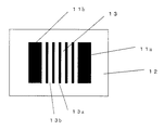
ここで用いられるグレートーンマスクとしては、半透光部が微細パターンで形成されている構造のものが知られている。例えば図5に示されるように、ソース/ドレインに対応する遮光部11a、11bと、透光部12と、チャネル部に対応する半透光部(グレートーン部)13とを有し、半透光部13は、グレートーンマスクを使用するLCD用露光機の解像限界以下の微細パターンからなる遮光パターン13aを形成した領域である。遮光部11a、11bと遮光パターン13aはともにクロムやクロム化合物等の同じ材料からなる同じ厚さの膜から通常形成されている。グレートーンマスクを使用するLCD用露光機の解像限界は、ステッパ方式の露光機で約3μm、ミラープロジェクション方式の露光機で約4μmである。このため、例えば、図5で半透光部13における透過部13bのスペース幅を3μm未満、遮光パターン13aのライン幅を露光機の解像限界以下の3μm未満とする。
As a gray-tone mask used here, one having a structure in which a semi-translucent portion is formed in a fine pattern is known. For example, as shown in FIG. 5, the light-shielding portions 11a and 11b corresponding to the source / drain, the
ところが、上述の微細パターンタイプの半透光部は、グレートーン部分の設計、具体的には遮光部と透光部の中間的なハーフトーン効果を持たせるための微細パターンをライン・アンド・スペースタイプにするのかドット(網点)タイプにするのか、或いはその他のパターンにするのかの選択があり、さらにライン・アンド・スペースタイプの場合、線幅をどのくらいにするのか、光が透過する部分と遮光される部分の比率をどうするか、全体の透過率をどの程度に設計するかなど非常に多くのことを考慮し設計を行わなくてはならなかった。また、マスク製造においても線幅の中心値の管理及びマスク内の線幅のばらつき管理と非常に難しい生産技術が要求されていた。 However, the above-mentioned fine pattern type semi-transmission part is a line-and-space type design for the gray tone part, specifically, a fine pattern for providing an intermediate halftone effect between the light-shielding part and the light-transmission part. There is a choice between a dot (halftone dot) type or another pattern, and in the case of the line and space type, how much the line width is to be set, and the part through which light is transmitted is blocked. The design had to be made in consideration of many things, such as what should be done with the ratio of the parts to be measured and how much the overall transmittance should be designed. Also in mask manufacturing, management of the center value of the line width and management of line width variation within the mask and extremely difficult production techniques have been required.
そこで、ハーフトーン露光したい部分を半透過性のハーフトーン膜(半透光膜)とすることが従来提案されている。このハーフトーン膜を用いることでハーフトーン部分の露光量を少なくしてハーフトーン露光することが出来る。ハーフトーン膜に変更することで、設計においては全体の透過率がどのくらい必要かを検討するのみで済み、マスクにおいてもハーフトーン膜の膜種であるとか膜厚を選択するだけでマスクの生産が可能となる。従って、マスク製造ではハーフトーン膜の膜厚制御を行うだけで済み、比較的管理が容易である。また、ハーフトーン膜であればフォトリソ工程により容易にパターニングできるので、複雑なパターン形状であっても可能となる。 Therefore, it has been conventionally proposed to use a semi-transmissive half-tone film (semi-transmissive film) for a portion to be subjected to half-tone exposure. By using this halftone film, halftone exposure can be performed while reducing the exposure amount of the halftone portion. By changing to a halftone film, it is only necessary to consider how much the overall transmittance is necessary in the design, and it is possible to produce a mask only by selecting the film type of the halftone film and the film thickness. It becomes possible. Therefore, in mask manufacturing, it is only necessary to control the film thickness of the halftone film, and management is relatively easy. Further, since a halftone film can be easily patterned by a photolithography process, even a complicated pattern shape is possible.
従来提案されているハーフトーン膜タイプのグレートーンマスクの製造方法は、以下のような方法である。ここでは、一例として図6に示すようなLCD基板用のパターン100を挙げて説明する。パターン100は、パターン101a、101bからなる遮光部パターン101と、この遮光部のパターン101a,101b間の半透光部パターン103と、これらパターンの周囲に形成される透光部パターン102とで構成されている。
A conventionally proposed method for manufacturing a halftone film type gray tone mask is as follows. Here, an
まず、透明基板上に半透光膜及び遮光膜を順次形成したマスクブランクスを準備し、このマスクブランクス上にレジスト膜を形成する。次に、パターン描画を行って、現像することにより、上記パターン100の遮光部パターン101及び半透光部パターン103に対応する領域にレジストパターンを形成する。次いで、適当な方法でエッチングすることにより、上記レジストパターンが形成されていない透光部パターン102に対応する領域の遮光膜とその下層の半透光膜が除去されて、図7(1)に示すようなパターンが形成される。すなわち、透光部202が形成され、同時に、前記パターン100の遮光部と半透光部に対応する領域の遮光パターン201が形成される。残存するレジストパターンを除去してから、再び、レジスト膜を基板上に形成し、パターン描画を行って、現像することにより、今度は前記パターン100の遮光部パターン101に対応する領域にレジストパターンを形成する。次いで、適当なエッチングにより、レジストパターンの形成されていない半透光部の領域の遮光膜のみを除去する。これにより、図7(2)に示すように前記パターン100に対応するパターンが形成される。すなわち、半透光膜のパターン203による半透光部が形成され、同時に、遮光部のパターン201a、201bが形成される。
First, a mask blank in which a semi-transparent film and a light-shielding film are sequentially formed on a transparent substrate is prepared, and a resist film is formed on the mask blank. Next, a pattern is drawn and developed to form a resist pattern in a region corresponding to the light
また、下記特許文献1には、上述の2度目のフォトリソ工程で、半透光部の領域の遮光膜のみをエッチングにより除去する際に、下層の半透光膜の膜減りを防止するために、マスクブランクスにおける透明基板上の半透光膜と遮光膜との間にエッチングストッパー膜を設けることが開示されている。
Further, in
しかしながら、このような従来のグレートーンマスク製造方法によると、遮光膜と半透光膜に例えば主成分が同じ材料(例えばクロムとクロム化合物など)を用いた場合、遮光膜と半透光膜のエッチング特性が近似しているので、前述の2度目のフォトリソ工程で、半透光部の領域の遮光膜のみをエッチングにより除去する際のエッチングの終点の判断が難しく、エッチングが足りないと半透光膜上に遮光膜が残ってしまい、エッチングがオーバーであると半透光膜の膜減りが起こり、何れにしても所望の半透光性が得られないという問題がある。従って、遮光膜及び半透光膜は少なくともエッチング特性が異なる材料の組合せを選択する必要があり、材料選択の幅が制約される。また、このように遮光膜及び半透光膜にエッチング特性が異なる材料の組合せを選択したとしても、上述の半透光膜の膜減りを完全に防止することが出来るわけではない。 However, according to such a conventional gray-tone mask manufacturing method, when the light shielding film and the semi-transparent film are made of, for example, the same material (for example, chromium and chromium compound), the light shielding film and the semi-transparent film are formed. Since the etching characteristics are approximate, it is difficult to determine the end point of etching when only the light-shielding film in the region of the semi-transparent portion is removed by etching in the second photolithography process described above. If the light-shielding film remains on the optical film and the etching is over, the semi-transparent film is reduced, and in any case, the desired semi-transparent property cannot be obtained. Therefore, it is necessary to select a combination of materials having different etching characteristics at least for the light shielding film and the semi-transparent film, and the range of material selection is limited. Further, even if a combination of materials having different etching characteristics is selected for the light-shielding film and the semi-transparent film as described above, it is not possible to completely prevent the above-described reduction of the semi-transparent film.
この場合、上記特許文献1に記載のように、使用するマスクブランクスにおける透明基板上の半透光膜と遮光膜との間にエッチングストッパー膜を設けることにより、半透光部領域の遮光膜のエッチングを多少オーバー気味に行っても下層の半透光膜の膜減りを防ぐことができる。しかし、使用するマスクブランクスの層構成が、半透光膜、エッチングストッパー膜及び遮光膜の3層となり、成膜が3段階必要で、製造コストを圧迫する。また、全体の膜厚が厚くなるため、アスペクト比(パターン寸法と高さの比)が大きく、その結果遮光部のパターン形状やパターン精度が悪くなり、またエッチング時間が長くなるという問題もある。また、遮光膜のエッチング後、残存するエッチングストッパー膜を除去する際に、やはり下地の半透光膜の膜減りの問題が生じる。エッチングストッパー膜が残っていても半透光膜の透過率に影響を与えないような材料であれば、そのまま除去せずに残しておくことも出来るが、エッチングストッパー膜の材料や膜厚が制約される。
In this case, as described in
このような問題を解決できるグレートーンマスクとして、本出願人は先に、遮光部が、透明基板上に設けられた遮光膜及びその上に成膜された半透光膜より形成され、半透光部は、半透光部に対応する領域を露出させた透明基板上に成膜された半透光膜より形成されているグレートーンマスクを提案した(特願2004−65115)。
このグレートーンマスクは次のようにして製造することができる(図8参照)。
As a gray-tone mask that can solve such a problem, the applicant of the present invention firstly formed a light-shielding portion from a light-shielding film provided on a transparent substrate and a semi-transparent film formed thereon. The light part proposed the gray tone mask formed from the semi-transparent film formed on the transparent substrate which exposed the area | region corresponding to a semi-transparent part (Japanese Patent Application No. 2004-65115).
This gray tone mask can be manufactured as follows (see FIG. 8).
まず、ガラス基板等の透明基板21上に、例えばクロム(Cr)を主成分とする材料を用いた遮光膜22を形成したマスクブランク20の上に、電子線用のポジ型レジスト膜を形成し、所定のパターン描画、現像を行って、レジストパターン23cを形成する(図8(a)(b)参照)。このレジストパターン23cは、半透光部を形成する領域(図8に図示するBの領域)ではレジストが除去され、遮光部を形成する領域(図8に図示するAの領域)及び透光部を形成する領域(図8に図示するCの領域)にはレジストが残存する。
次に、形成されたレジストパターン23cをマスクとして、遮光膜22をエッチングして、遮光部及び透光部に対応する遮光膜パターン22bを形成する(図8(c)参照)。半透光部に対応する領域(B領域)では、上記遮光膜22のエッチングにより下地の透明基板21が露出した状態である。残存するレジストパターン23cは、酸素によるアッシング或いは濃硫酸などを用いて除去する(図8(d)参照)。
First, on a
Next, using the formed resist
次に、以上のようにして得られた透明基板21上に遮光膜パターン22bを有する基板上の全面に半透光膜24を成膜する(図8(e)参照)。これにより、半透光部に対応する領域では、露出した透明基板21上に直接半透光膜24が成膜されて半透光部を形成する。
次に、再び全面に前記ポジ型レジスト膜を形成し、2回目の描画を行う。描画後、これを現像して、透光部(C領域)ではレジストが除去され、遮光部及び半透光部にはレジストが残存するレジストパターン23dを形成する(図8(f)参照)。
Next, the
Next, the positive resist film is formed again on the entire surface, and the second drawing is performed. After drawing, this is developed to form a resist
次に、形成されたレジストパターン23dをマスクとして、透光部となるC領域の半透光膜24及び遮光膜22bをエッチングにより除去する。これにより、遮光部は透光部と画され、遮光部(A領域)及び透光部(C領域)が形成される(図8(g)参照)。残存するレジストパターン23dは、酸素アッシング等を用いて除去する(図8(h)参照)。
以上のようにして上記グレートーンマスク40が出来上がる。
このように、半透光部は、半透光部に対応する領域を露出させた透明基板上に直接半透光膜を成膜してなるため、従来のように半透光部を形成する場合に、上層の遮光膜のみをエッチングにより除去して下層の半透光膜を露出させる必要がなくなり、それゆえ遮光膜と半透光膜を共にエッチング特性が同じか或いは近似した膜材料で形成することもでき、膜材料の選択の幅が広がる。従って、従来の遮光膜と半透光膜の間に設けていたエッチングストッパー膜は不要であり、全体の膜厚を薄く出来て、アスペクト比を小さくすることができる。
Next, using the formed resist
The
As described above, the semi-transparent portion is formed by directly forming the semi-transparent film on the transparent substrate in which the region corresponding to the semi-transparent portion is exposed. In this case, it is not necessary to remove only the upper light-shielding film by etching and expose the lower semi-transparent film. Therefore, both the light-shielding film and the semi-transparent film are formed of film materials having the same or similar etching characteristics. It is also possible to expand the range of choice of film material. Therefore, the etching stopper film provided between the conventional light-shielding film and the semi-transparent film is unnecessary, the entire film thickness can be reduced, and the aspect ratio can be reduced.
しかしながら、上記製造方法を実際に実施した場合、次のような問題点があった。即ち、遮光膜と半透光膜の膜材料のエッチング特性が同一又は近似している場合は、上述の図8(g)の工程において、透光部となるC領域の半透光膜24及び遮光膜22bのエッチングを同一エッチングガス(ドライエッチング)又は同一エッチング液(ウェットエッチング)で一度に或いは連続的に処理することが出来るが、実際には、上層の半透光膜24がエッチングされ、続いて下層の遮光膜22bがエッチングされている間に、側面が露出した半透光膜(半透光部となるB領域)のサイドエッチングが進み(図10のDで示すダメージ部分)、その結果半透光部のパターン形状を悪化させるという問題点があった。
However, when the above manufacturing method was actually carried out, there were the following problems. That is, when the etching characteristics of the film materials of the light-shielding film and the semi-transparent film are the same or similar, in the process of FIG. Etching of the
そのような半透光膜のサイドエッチングを防止するために、前述の方法のように1回目のエッチングで半透光部を形成する領域をエッチングし、2回目のエッチングで透光部を形成する領域をエッチングするのではなく、1回目のエッチングで半透光部及び透光部を形成する領域をエッチングし、2回目のエッチングで透光部を形成する領域をエッチングする、次のような方法により同様のグレートーンマスクを製造することが考えられる(図9参照)。 In order to prevent such side etching of the semi-transparent film, the region where the semi-transparent portion is formed is etched by the first etching and the translucent portion is formed by the second etching as described above. Instead of etching the region, the region where the translucent part and the light transmitting part are formed is etched by the first etching, and the region where the light transmitting part is formed is etched by the second etching. It is conceivable to manufacture a similar gray-tone mask by (see FIG. 9).
まず、ガラス基板等の透明基板21上に、例えばクロム(Cr)を主成分とする材料を用いた遮光膜22を形成したマスクブランク20の上に、ポジ型レジスト膜を形成し、所定のパターン描画、現像を行って、レジストパターン23aを形成する(図9(a)(b)参照)。このレジストパターン23aは、半透光部を形成する領域(図9に図示するBの領域)及び透光部を形成する領域(図9に図示するCの領域)を露出させ、遮光部を形成する領域(図9に図示するAの領域)にのみレジストが残存する。
次に、このレジストパターン23aをマスクとして、遮光膜22をエッチングして、遮光部に対応する遮光膜パターン22aを形成する(図9(c)参照)。半透光部及び透光部に対応する領域では、上記遮光膜22のエッチングにより下地の透明基板21が露出した状態である。残存するレジストパターン23aは、酸素によるアッシング或いは濃硫酸などを用いて除去する(図9(d)参照)。
First, on a
Next, using the resist
次に、以上のようにして得られた透明基板21上に遮光膜パターン22aを有する基板上の全面に半透光膜24を成膜する(図9(e)参照)。
再び全面に前記ポジ型レジスト膜を形成し、2回目の描画を行う。描画後、これを現像して、透光部(C領域)を露出させ、遮光部及び半透光部にレジストが残存するレジストパターン23bを形成する(図9(f)参照)。
次に、形成されたレジストパターン23bをマスクとして、透光部となるC領域の半透光膜24をエッチングにより除去する(図9(g)参照)。残存するレジストパターン23bは、酸素アッシング等を用いて除去する(図9(h)参照)。
以上のようにして上記グレートーンマスク30が出来上がる。
Next, the
The positive resist film is again formed on the entire surface, and the second drawing is performed. After drawing, this is developed to expose the translucent part (C region) and form a resist
Next, using the formed resist
The
この図9に示す方法を用いた場合、2回目のエッチングでは半透光膜のみをエッチングすればよく、前述の図8に示す方法のように2回目のエッチングで半透光膜、遮光膜の順に両方をエッチングする必要がなくなる。
しかしながら、図9に示す方法を用いた場合、遮光膜と半透光膜のエッチング特性が同一又は近似していると、透光部に対応する領域の半透光膜24をエッチングする工程(図9(g))において、実際には、隣接する断面が露出している遮光膜22aのサイドエッチングが進み、図11中のDで示すように断面形状を悪化させることがある。
そこで本発明の目的は、従来の問題点を解消して、パターン形状及び断面形状が良好なハーフトーン膜タイプのグレートーンマスク及びその製造方法を提供することである。
When the method shown in FIG. 9 is used, only the semi-transparent film needs to be etched in the second etching, and the semi-transparent film and the light-shielding film are etched in the second etching as in the method shown in FIG. It is not necessary to etch both in turn.
However, when the method shown in FIG. 9 is used, if the etching characteristics of the light-shielding film and the semi-transparent film are the same or similar, the process of etching the
SUMMARY OF THE INVENTION Accordingly, an object of the present invention is to provide a halftone film type gray-tone mask having a good pattern shape and cross-sectional shape, and a method for manufacturing the same, by solving conventional problems.
上記課題を解決するため、本発明は以下の構成を有する。
(構成1)遮光部、透光部及び半透光部からなるパターンを有するグレートーンマスクの製造方法であって、透明基板上に形成された遮光膜の上に、遮光部を形成するための第1のレジストパターンを形成する工程と、前記第1のレジストパターンをマスクとして前記遮光膜をエッチングして遮光膜パターンを形成し、残存した第1のレジストパターンを剥離する工程と、前記遮光膜パターン上に半透光膜を形成し、その上に透光部を形成するための第2のレジストパターンを形成する工程と、前記第2のレジストパターンをマスクとして前記半透光膜をエッチングして半透光膜パターンを形成し、残存した第2のレジストパターンを剥離する工程と、を有し、前記半透光膜を構成する材料は、前記遮光膜を構成する材料よりも、前記半透光膜をエッチングするためのエッチャントに対し、エッチングレートが大きい材料であることを特徴とするグレートーンマスクの製造方法である。
(構成2)前記遮光膜はクロム(Cr)を主成分とする材料からなり、前記半透光膜はクロム(Cr)と窒素(N)とを含む材料からなることを特徴とする構成1に記載のグレートーンマスクの製造方法である。
(構成3)前記半透光膜パターンを形成する際のエッチングに対する半透光膜の遮光膜に対するエッチング選択比(半透光膜のエッチングレート/遮光膜のエッチングレート)が2以上であることを特徴とする構成1又は2に記載のグレートーンマスクの製造方法である。
In order to solve the above problems, the present invention has the following configuration.
(Configuration 1) A method for manufacturing a gray-tone mask having a pattern composed of a light-shielding part, a light-transmitting part, and a semi-light-transmitting part, for forming a light-shielding part on a light-shielding film formed on a transparent substrate Forming a first resist pattern, etching the light shielding film using the first resist pattern as a mask to form a light shielding film pattern, and peeling off the remaining first resist pattern; and the light shielding film Forming a semi-transparent film on the pattern, forming a second resist pattern for forming a translucent portion thereon, and etching the semi-transparent film using the second resist pattern as a mask; Forming a semi-transparent film pattern and peeling off the remaining second resist pattern, and the material constituting the semi-transparent film is more suitable than the material constituting the light-shielding film. Translucency The relative etchant for etching a method for manufacturing a gray-tone mask, wherein the etching rate is great material.
(Structure 2) The
(Configuration 3) An etching selection ratio of the semi-transparent film to the light-shielding film with respect to the etching for forming the semi-transparent film pattern (semi-transparent film etching rate / light-shielding film etching rate) is 2 or more. It is a manufacturing method of the gray tone mask of the
(構成4)前記半透光膜パターンを形成するためのエッチングに用いられるエッチング液と遮光膜パターンを形成するためのエッチングに用いられるエッチング液とが、同種のエッチング液で濃度が異なるものであることを特徴とする構成1乃至3の何れかに記載のグレートーンマスクの製造方法である。
(構成5)構成1乃至4の何れかに記載のグレートーンマスクの製造方法を用いて得られるグレートーンマスクであって、透明基板上に形成された遮光膜パターンと、その上に形成された半透光膜パターンを有し、前記遮光部は、少なくとも前記遮光膜パターンの遮光膜により形成され、前記半透光部は、前記半透光膜パターンの前記遮光膜パターンの基板露出部に形成された半透光膜により形成されていることを特徴とするグレートーンマスクである。
(構成6)構成1乃至4の何れかに記載のグレートーンマスクの製造方法に用いるためのグレートーンマスクブランクであって、透明基板上に、遮光膜パターンと、該遮光膜パターン上に形成された半透光膜とを有し、前記半透光膜を構成する材料は、前記遮光膜を構成する材料よりも、前記半透光膜をエッチングするためのエッチャントに対し、エッチングレートが大きい材料であることを特徴とするグレートーンマスクブランクである。
(Configuration 4) The etching solution used for the etching for forming the semi-transparent film pattern and the etching solution used for the etching for forming the light-shielding film pattern have different concentrations in the same kind of etching solution. The method of manufacturing a gray-tone mask according to any one of
(Configuration 5) A gray-tone mask obtained by using the method of manufacturing a gray-tone mask according to any one of
(Configuration 6) A gray-tone mask blank for use in the method for manufacturing a gray-tone mask according to any one of
請求項1の発明によれば、透明基板上に形成された遮光膜の上に、遮光部を形成するための第1のレジストパターンを形成する工程と、前記第1のレジストパターンをマスクとして前記遮光膜をエッチングして遮光膜パターンを形成し、残存した第1のレジストパターンを剥離する工程と、前記遮光膜パターン上に半透光膜を形成し、その上に透光部を形成するための第2のレジストパターンを形成する工程と、前記第2のレジストパターンをマスクとして前記半透光膜をエッチングして半透光膜パターンを形成し、残存した第2のレジストパターンを剥離する工程とを有するグレートーンマスクの製造方法にあって、半透光膜を構成する材料は、遮光膜を構成する材料よりも、半透光膜をエッチングするためのエッチャントに対しエッチングレートが大きい材料としたので、上記半透光膜のエッチングの際に断面が露出している遮光膜のサイドエッチングの進行を抑制でき、その結果、平面視のパターン形状だけでなく断面形状も良好なグレートーンマスクが得られる。また、このグレートーンマスクを用いて製造したLCD等は、特性が良好で高信頼性のものが得られる。 According to the first aspect of the present invention, a step of forming a first resist pattern for forming a light-shielding portion on the light-shielding film formed on the transparent substrate, and the first resist pattern as a mask Etching the light shielding film to form a light shielding film pattern, removing the remaining first resist pattern, forming a semi-translucent film on the light shielding film pattern, and forming a translucent portion thereon Forming the second resist pattern, etching the semi-transparent film using the second resist pattern as a mask to form a semi-transparent film pattern, and peeling the remaining second resist pattern The material constituting the semi-transparent film is more etched than the material constituting the light-shielding film with respect to the etchant for etching the semi-transparent film. Since the material has a high rate, it is possible to suppress the progress of side etching of the light shielding film whose cross section is exposed when etching the semi-transparent film, and as a result, not only the pattern shape in plan view but also the cross sectional shape is good. A gray tone mask can be obtained. Further, an LCD or the like manufactured using this gray tone mask has good characteristics and high reliability.
請求項2の発明によれば、前記遮光膜はクロム(Cr)を主成分とする材料とし、前記半透光膜はクロム(Cr)と窒素(N)とを含む材料としたことにより、半透光膜は、遮光膜よりも、半透光膜をエッチングするためのエッチャントに対しエッチングレートが大きくなり、上記半透光膜のエッチングの際に断面が露出している遮光膜のサイドエッチングの進行を抑制でき、パターン形状及び断面形状の良好なグレートーンマスクが得られる。
請求項3の発明によれば、前記半透光膜パターンを形成する際のエッチングに対する半透光膜の遮光膜に対するエッチング選択比(半透光膜のエッチングレート/遮光膜のエッチングレート)が2以上であることにより、上記半透光膜のエッチングの際に断面が露出している遮光膜のサイドエッチングの進行を特に好適に抑制できるため、パターン形状及び断面形状の良好なグレートーンマスクが得られる。
According to the invention of
According to the third aspect of the present invention, the etching selectivity of the semi-transparent film to the light-shielding film with respect to the etching at the time of forming the semi-transparent film pattern (semi-transparent film etching rate / light-shielding film etching rate) is 2. As described above, since the progress of side etching of the light-shielding film whose cross section is exposed during the etching of the semi-translucent film can be particularly preferably suppressed, a gray-tone mask having a good pattern shape and cross-sectional shape can be obtained. It is done.
請求項4の発明によれば、前記半透光膜パターンを形成するためのエッチングに用いられるエッチング液と遮光膜パターンを形成するためのエッチングに用いられるエッチング液とが、同種のエッチング液で濃度が異なるものを使用することにより、遮光膜と半透光膜のそれぞれのエッチングレートをエッチング制御性が好ましくなるように容易に調整することが出来る。
According to invention of
請求項5の発明によれば、本発明により得られるグレートーンマスクは、透明基板上に形成された遮光膜パターンと、その上に形成された半透光膜パターンを有し、前記遮光部は、少なくとも前記遮光膜パターンの遮光膜により形成され、前記半透光部は、前記半透光膜パターンの前記遮光膜パターンの基板露出部に形成された半透光膜により形成されているので、パターン形状や断面形状が良好なものが得られることに加えて、従来のように半透光部を形成する場合に、上層の遮光膜のみをエッチングにより除去して下層の半透光膜を露出させる必要がなくなり、従来の遮光膜と半透光膜の間に設けていたエッチングストッパー膜は不要であり、全体の膜厚を薄く出来て、アクペクト比を小さくすることができ、全体としてパターン精度を向上できる。
請求項6の発明によれば、透明基板上に、遮光膜パターンと、該遮光膜パターン上に形成された半透光膜とを有し、半透光膜を構成する材料は、遮光膜を構成する材料よりも、半透光膜をエッチングするためのエッチャントに対しエッチングレートが大きい材料としたグレートーンマスクブランクであって、本発明のグレートーンマスクの製造方法に好適に用いることができる。
According to invention of
According to invention of
以下、本発明を実施の形態により説明する。
本発明のグレートーンマスクの製造方法は、遮光部、透光部及び半透光部からなるパターンを有するグレートーンマスクの製造方法であって、透明基板上に形成された遮光膜の上に、遮光部を形成するための第1のレジストパターンを形成する工程と、前記第1のレジストパターンをマスクとして前記遮光膜をエッチングして遮光膜パターンを形成し、残存した第1のレジストパターンを剥離する工程と、前記遮光膜パターン上に半透光膜を形成し、その上に透光部を形成するための第2のレジストパターンを形成する工程と、前記第2のレジストパターンをマスクとして前記半透光膜をエッチングして半透光膜パターンを形成し、残存した第2のレジストパターンを剥離する工程とを有する。具体的には、前述の図9に示す製造方法を適用することができる。そこで、再度、図9を参照しながら本発明を説明する。
Hereinafter, the present invention will be described with reference to embodiments.
The graytone mask manufacturing method of the present invention is a graytone mask manufacturing method having a pattern composed of a light-shielding portion, a light-transmitting portion, and a semi-light-transmitting portion, on a light-shielding film formed on a transparent substrate, Forming a first resist pattern for forming a light-shielding portion; etching the light-shielding film using the first resist pattern as a mask to form a light-shielding film pattern; and stripping the remaining first resist pattern Forming a translucent film on the light shielding film pattern, forming a second resist pattern for forming a translucent portion thereon, and using the second resist pattern as a mask Etching the semi-transparent film to form a semi-transparent film pattern, and peeling off the remaining second resist pattern. Specifically, the manufacturing method shown in FIG. 9 can be applied. Therefore, the present invention will be described again with reference to FIG.
本発明では、透明基板21上に遮光膜22を形成したマスクブランク20を用いる(図9(a)参照)。本発明では、遮光膜22の材料としては、クロム(Cr)単体、又は、エッチング特性や基板への付着力を考慮して、クロムに窒素、炭素、フッ素、酸素等から選ばれる一種又は二種以上の元素を含有したものであってもよい。さらに、組成の異なる膜の積層膜や、組成を膜厚方向で変えた組成傾斜膜であってもよい。尚、遮光膜は、表面又は表裏面に酸化クロム等の反射防止膜を有するのが一般的である。また、遮光膜22の膜厚は、マスクを使用するときの露光光に対し、十分な光学濃度を有するような膜厚とする。例えば、露光光がi線の場合、反射防止膜付き遮光膜は、80〜110nm程度とすることが好ましい。
透明基板21としては、例えば石英基板が用いられるが、ソーダライムガラス、無アルカリガラス等でも良い。透明基板21の大きさは、マスクの使用目的によって異なるが、例えばLSI製造用には通常4〜8インチ角のもの、LCD用大型基板の場合は短辺が300mm以上のもので、例えば330mm×450mm〜1400mm×1600mmのものである。
In the present invention, a mask blank 20 having a
As the
上記マスクブランク20は、透明基板21上に遮光膜22を形成することで得られるが、その成膜方法は、蒸着法、スパッタ法、CVD(化学的気相成長)法など、膜種に適した方法を適宜選択すればよい。
このマスクブランク20上の全面に、例えばレーザ描画用のポジ型レジスト膜を形成し、所定のパターン描画、現像を行って、半透光部を形成する領域(図9のB領域)及び透光部を形成する領域(図9のC領域)を露出させ、遮光部を形成する領域(図9のA領域)にのみレジストが残存するレジストパターン23aを形成する(図9(b)参照)。
The mask blank 20 is obtained by forming the
A positive resist film for laser drawing, for example, is formed on the entire surface of the mask blank 20, and a predetermined pattern is drawn and developed to form a region (B region in FIG. 9) and a light-transmitting portion. A region for forming a portion (region C in FIG. 9) is exposed, and a resist
次に、このレジストパターン23aをマスクとして、遮光膜22をエッチングして、遮光部を形成する領域に対応する遮光膜パターン22aを形成する(図9(c)参照)。半透光部及び透光部に対応する領域では、上記遮光膜22のエッチングにより下地の透明基板21が露出した状態となる。尚、遮光膜22のエッチングにはウェットエッチングを用いることが、特に大型の液晶デバイス製造用のフォトマスクを製造する上では、コスト面で好ましい。遮光膜22のウェットエッチングには、通常クロム系薄膜のウェットエッチングに用いられる硝酸第2セリウムアンモニウム系のエッチング液を用いることが出来る。
残存するレジストパターン23aは、酸素によるアッシング或いは濃硫酸などを用いて除去する(図9(d)参照)。
Next, using the resist
The remaining resist
次に、以上のようにして得られた透明基板21上に遮光膜パターン22aを有する基板上の全面に半透光膜24を成膜する(図9(e)参照)。本発明では、半透光膜24を構成する材料は、前記遮光膜22を構成する材料よりも、半透光膜24をエッチングするためのエッチャント(例えばウェットエッチングするためのエッチング液)に対しエッチングレートが大きい材料である。このような半透光膜24の材料としては、クロム(Cr)に、クロムのエッチング液に対してエッチングレートを大きく(速く)するような添加元素を含む材料が、半透光膜24のエッチングレートを好適に調整することができるので、好ましく挙げられる。エッチングレートを大きく(速く)するような添加元素としては、窒素、酸素(尚、酸素は添加の仕方によりエッチングレートを小さく(遅く)する作用を示す場合もある)等がある。但し、酸素を含むことにより、膜の結晶グレインが大きくなり膜応力が大きくなることがあるため、窒素を含ませることにより半透光膜のエッチングレートを調整する方がより好ましい。半透光膜として、クロムと窒素を含む材料を用いる場合、クロムと窒素との比率は、原子比でCr:N=50:50〜10:90とすることが好ましい。
また、半透光膜24は、前記遮光膜22と同種のエッチング液でエッチングできる材料であることが好ましい。
Next, the
Further, the
半透光膜24の成膜方法については、前述の遮光膜22の場合と同様、蒸着法、スパッタ法、CVD(化学的気相成長)法など、膜種に適した方法を適宜選択すればよい。また、半透光膜24の膜厚に関しては、特に制約はないが、所望の半透光性が得られるように最適化された膜厚で形成すればよい。尚、透過率、エッチング特性、遮光膜パターン上への成膜特性、膜応力、膜厚分布等を考慮した場合、通常30〜250Åの範囲とするのが適当である。半透光膜24としては、薄膜で、例えば露光光のi線(365nm)に対し、透光部の透過率を100%とした場合に透過率20〜60%程度の半透光性が得られるものが挙げられ、二種の膜厚のレジストパターンを形成する場合は、一般的には40〜60%程度に設定されるが、半透光膜の透過率はこれに限定される必要はない。半透光部の透過性をどの程度に設定するかはマスクの使用目的に応じた設計上の問題である。半透光膜24の透過率は、膜厚と組成(例えば窒素含有量)により調整することが出来る。
As for the method for forming the
次に、再び全面に前記ポジ型レジスト膜を形成し、2回目の描画を行う。描画後、これを現像して、透光部(C領域)を露出させ、遮光部及び半透光部にはレジストが残存するレジストパターン23bを形成する(図9(f)参照)。
次に、形成されたレジストパターン23bをマスクとして、透光部となるC領域の半透光膜24をエッチングにより除去する(図9(g)参照)。半透光膜24のエッチングについても、ウェットエッチングを用いることが、特に大型の液晶デバイス製造用のフォトマスクを製造する上では、コスト面で好ましい。半透光膜24のウェットエッチングには、前記遮光膜22と同様に、通常クロム系薄膜のウェットエッチングに用いられる硝酸第2セリウムアンモニウム系のエッチング液を用いることが出来る。尚、前記遮光膜22と半透光膜24とで、それぞれのエッチングレートをエッチング制御性が好ましくなるように調整するために、同種のエッチング液でその濃度がそれぞれ異なるものを使用してもよい。例えば、半透光膜の材料としてクロムに窒素を含有させた場合、遮光膜をエッチングするためのエッチング液をその濃度のまま使用すると、半透光膜のエッチングレートが速すぎてエッチング制御性が悪いため、遮光膜のエッチング液を適宜希釈して用いることが好ましい。
Next, the positive resist film is formed again on the entire surface, and the second drawing is performed. After drawing, this is developed to expose the light transmitting portion (C region), and a resist
Next, using the formed resist
本発明では、半透光膜24のエッチングに対する、半透光膜24の遮光膜22に対するエッチング選択比(半透光膜24のエッチングレート/遮光膜22のエッチングレート)が2以上であることが特に好ましい。
残存するレジストパターン23bは、酸素アッシング等を用いて除去する(図9(h)参照)。
以上のようにして本発明によるグレートーンマスクが出来上がる。
In the present invention, the etching selection ratio of the
The remaining resist
The gray tone mask according to the present invention is completed as described above.
本発明では、半透光膜を構成する材料は、遮光膜を構成する材料よりも、半透光膜をエッチングするためのエッチャントに対しエッチングレートが大きい材料としたので、上述の透光部に対応する領域(C領域)の半透光膜24をエッチングする際(図9(g))に、隣接する遮光部の断面が露出している遮光膜22aのサイドエッチングの進行を抑制することができ、その結果、平面視のパターン形状だけでなく断面形状も良好なグレートーンマスクが得られる。
なお、本実施の形態では、ポジ型のレジストを用いた場合を例示したが、ネガ型レジストを用いてもよい。この場合、描画データが反転するだけで、工程は上述と全く同様にして実施できる。
In the present invention, the material that constitutes the semi-transparent film is a material that has a higher etching rate than the material that constitutes the light-shielding film with respect to the etchant for etching the semi-transparent film. When etching the
In this embodiment, the case where a positive resist is used is exemplified, but a negative resist may be used. In this case, the process can be carried out in exactly the same manner as described above only by reversing the drawing data.
(実施例)
以下、具体的な実施例を挙げて説明する。
透明基板としては、石英基板を使用し、大きさはLCD用大型基板サイズである330mm×450mm×10mmとした。
遮光膜の材料は、クロム単体とし、透明基板上に、i線(365nm)に対し十分な遮光性が得られるような膜厚でスパッタ成膜した。スパッタガスはAr100%とした。
(Example)
Hereinafter, specific examples will be described.
A quartz substrate was used as the transparent substrate, and the size was 330 mm × 450 mm × 10 mm, which is a large substrate size for LCD.
The light-shielding film was made of chromium alone, and was formed by sputtering on a transparent substrate so as to obtain a sufficient light-shielding property against i-line (365 nm). The sputtering gas was
半透光膜の材料は、クロムと窒素を含む材料とし、遮光膜パターンが形成された基板上にスパッタ成膜により形成した。この際、スパッタガスとしては、Arと窒素(N2)の混合ガスとし、その混合比(体積比)は、Ar:N2=0:100、20:80、40:60の3通りとし、膜厚は、グレートンマスクの要求特性の一例であるi線における透過率が40〜50%の範囲になるような膜厚として、それぞれ、74nm、76nm、78nmに成膜した。その結果、何れの半透光膜についても43%付近の透過率が得られた。また、膜組成については、スパッタガス組成が、Ar:N2=40:60の場合は、Cr:N=約40:60(原子%比)、Ar:N2=20:80の場合は、Cr:N=約20:80(原子%比)、Ar:N2=0:100の場合は、Cr:N=約10:90(原子%比)となった。
以上の材料を使用し、前述の図9に示す製造工程に従って、グレートーンマスクを製造した。尚、遮光膜のエッチングには、硝酸第2セリウムアンモニウム系エッチング液を使用し、半透光膜のエッチングには、遮光膜と同じエッチング液を蒸留水で適宜希釈したものを使用した。
The material of the semi-transparent film was a material containing chromium and nitrogen, and was formed by sputtering film formation on the substrate on which the light shielding film pattern was formed. At this time, the sputtering gas is a mixed gas of Ar and nitrogen (N 2 ), and the mixing ratio (volume ratio) is Ar: N 2 = 0: 100, 20:80, 40:60, The film thicknesses were set to 74 nm, 76 nm, and 78 nm, respectively, so that the transmittance at i-line, which is an example of the required characteristics of the Grayton mask, was in the range of 40 to 50%. As a result, a transmittance of about 43% was obtained for any semi-transparent film. Regarding the film composition, when the sputtering gas composition is Ar: N 2 = 40: 60, Cr: N = about 40:60 (atomic% ratio), and when Ar: N 2 = 20: 80, When Cr: N = about 20:80 (atomic% ratio) and Ar: N 2 = 0: 100, Cr: N = about 10:90 (atomic% ratio) was obtained.
Using the above materials, a gray-tone mask was manufactured according to the manufacturing process shown in FIG. For etching the light shielding film, a ceric ammonium nitrate-based etching solution was used, and for etching the semi-transparent film, the same etching solution as that for the light shielding film was appropriately diluted with distilled water.
図1は、半透光膜のエッチング液として、2%、4%、6%、9%の希釈液をそれぞれ使用した場合の各濃度における半透光膜のエッチングレート及び、膜厚が5nmと20nmの場合のエッチング時間の関係をプロットしたものである。尚、図1に示す値は、上記3種類の膜組成の半透光膜における平均値である。
図1に示されるように、エッチング液の濃度が低いほどエッチングレートが小さくなるので、エッチング時間を適当な範囲で長くすることも出来、エッチング制御性が良好なエッチング時間(例えば20秒〜2分程度)とするための希釈濃度を選択することが出来る。尚、半透光膜と遮光膜とのエッチング選択比は、このエッチング液の希釈により大きく影響することはなかった。
FIG. 1 shows the etching rate of the semi-transparent film and the film thickness of 5 nm when the dilutions of 2%, 4%, 6%, and 9% are used as the semi-transparent film etching liquid, respectively. The relationship of the etching time in the case of 20 nm is plotted. In addition, the value shown in FIG. 1 is an average value in the semi-transparent film having the above three kinds of film compositions.
As shown in FIG. 1, the lower the etching solution concentration, the lower the etching rate. Therefore, the etching time can be extended within an appropriate range, and the etching time with good etching controllability (for example, 20 seconds to 2 minutes). The dilution concentration can be selected. Note that the etching selectivity between the semi-transparent film and the light-shielding film was not greatly affected by the dilution of the etching solution.
また、図2は、上記各希釈液を用いた場合の半透光膜と遮光膜との平均エッチング選択比(半透光膜のエッチングレート(nm/sec)/遮光膜のエッチングレート(nm/sec))を各半透光膜の組成(横軸はスパッタガス組成で示している)毎にプロットしたものである。
図2の結果からは、半透光膜の成膜に用いるスパッタガス中のN2が60原子%以上では、上記のエッチング選択比が2以上とれることがわかる。
また、本実施例により得られたグレートーンマスクのパターンの断面形状を断面TEM観察したところ、断面形状は良好なものが得られていた。
FIG. 2 shows the average etching selectivity between the semi-transparent film and the light-shielding film (the semi-transparent film etching rate (nm / sec) / the light-shielding film etching rate (nm / sec)) is plotted for each semi-transparent film composition (the horizontal axis indicates the sputtering gas composition).
From the result of FIG. 2, it can be seen that when the N 2 in the sputtering gas used for forming the translucent film is 60 atomic% or more, the above etching selectivity can be 2 or more.
Further, when the cross-sectional shape of the gray-tone mask pattern obtained in this example was observed by cross-sectional TEM, a good cross-sectional shape was obtained.
さらに、図12は、上記実施例において、スパッタガス組成がAr:N2=0:100で成膜した窒化クロム膜について、透過率スペクトルを測定した結果のグラフである。また、エッチングレートを大きくすることが可能な酸化クロム膜についても透過率スペクトルを測定した結果のグラフを併せて示した。このグラフより、窒化クロム膜は、酸化クロム膜よりも、透過率の波長依存性が小さく、LCD用露光装置に用いられるブロード光源(g線、h線、i線なども含む)を用いた場合であっても、各々の波長に対してより均一な強度の低下での露光が可能であることがわかる。 Furthermore, FIG. 12 is a graph showing the result of measuring the transmittance spectrum of a chromium nitride film formed with a sputtering gas composition of Ar: N 2 = 0: 100 in the above example. A graph showing the result of measuring the transmittance spectrum of a chromium oxide film capable of increasing the etching rate is also shown. From this graph, the chromium nitride film has less wavelength dependency of the transmittance than the chromium oxide film, and when using a broad light source (including g-line, h-line, i-line, etc.) used in LCD exposure apparatus However, it can be seen that exposure can be performed with a more uniform intensity reduction for each wavelength.
21 透明基板
22 遮光膜
23a〜23d レジストパターン
24 半透光膜
20 マスクブランク
10、30、40 グレートーンマスク
100 マスクパターン
101 遮光部パターン
102 透光部パターン
103 半透光部パターン
21
Claims (2)
透明基板上に形成された遮光膜パターンと、その上に形成された半透光膜パターンを有し、前記遮光部は、少なくとも前記遮光膜パターンの遮光膜により形成され、前記半透光部は、前記半透光膜パターンの前記遮光膜パターンの基板露出部に形成された半透光膜により形成され、
該グレートーンマスクは、g線、h線、及びi線を含む光源を持つ露光装置によって露光されるものであり、かつ、
前記半透光膜は、クロム(Cr)と窒素(N)を含有し、i線からg線までの露光波長領域において、透過率変化が1.5%以下であることを特徴とするグレートーンマスク。 Shielding portion, a gray-tone mask TFT substrate manufacturing having a pattern of transparent portion and semitransparent portion, the channel portion formation region of the TFT substrate is thinner than the source drain forming regions, two kinds of thickness In a gray-tone mask for forming a resist pattern having
A light-shielding film pattern formed on the transparent substrate; and a semi-light-transmitting film pattern formed thereon; wherein the light-shielding part is formed by at least a light-shielding film of the light-shielding film pattern; , Formed by a semi-transparent film formed on a substrate exposed portion of the light-shielding film pattern of the semi-transparent film pattern,
The gray tone mask is exposed by an exposure apparatus having a light source including g-line, h-line, and i-line, and
The semi-transparent film contains chromium (Cr) and nitrogen (N), and has a transmittance change of 1.5% or less in an exposure wavelength region from i-line to g-line.
Priority Applications (1)
| Application Number | Priority Date | Filing Date | Title |
|---|---|---|---|
| JP2006049425A JP4919220B2 (en) | 2005-02-28 | 2006-02-25 | Gray tone mask |
Applications Claiming Priority (3)
| Application Number | Priority Date | Filing Date | Title |
|---|---|---|---|
| JP2005054352 | 2005-02-28 | ||
| JP2005054352 | 2005-02-28 | ||
| JP2006049425A JP4919220B2 (en) | 2005-02-28 | 2006-02-25 | Gray tone mask |
Related Child Applications (1)
| Application Number | Title | Priority Date | Filing Date |
|---|---|---|---|
| JP2011023432A Division JP5201762B2 (en) | 2005-02-28 | 2011-02-06 | Gray tone mask, gray tone mask manufacturing method, and pattern transfer method |
Publications (3)
| Publication Number | Publication Date |
|---|---|
| JP2006268035A JP2006268035A (en) | 2006-10-05 |
| JP2006268035A5 JP2006268035A5 (en) | 2007-10-04 |
| JP4919220B2 true JP4919220B2 (en) | 2012-04-18 |
Family
ID=37204002
Family Applications (1)
| Application Number | Title | Priority Date | Filing Date |
|---|---|---|---|
| JP2006049425A Active JP4919220B2 (en) | 2005-02-28 | 2006-02-25 | Gray tone mask |
Country Status (1)
| Country | Link |
|---|---|
| JP (1) | JP4919220B2 (en) |
Families Citing this family (19)
| Publication number | Priority date | Publication date | Assignee | Title |
|---|---|---|---|---|
| TWI569092B (en) * | 2005-12-26 | 2017-02-01 | Hoya Corp | A mask substrate and a mask for manufacturing a flat panel display device |
| CN101346664B (en) * | 2005-12-26 | 2011-12-14 | Hoya株式会社 | mask blank and photomask |
| JP4910828B2 (en) * | 2007-03-28 | 2012-04-04 | 大日本印刷株式会社 | Gradation mask |
| JP5115953B2 (en) * | 2007-03-30 | 2013-01-09 | Hoya株式会社 | Photomask blank and photomask |
| JP5105407B2 (en) * | 2007-03-30 | 2012-12-26 | Hoya株式会社 | Photomask blank, photomask and photomask manufacturing method |
| US8133641B2 (en) | 2007-05-11 | 2012-03-13 | Lg Innotek Co., Ltd. | Half tone mask having multi-half permeation part and a method of manufacturing the same |
| JP2009086385A (en) * | 2007-09-29 | 2009-04-23 | Hoya Corp | Photomask and method for manufacturing the same, and pattern transfer method |
| WO2009048089A1 (en) * | 2007-10-12 | 2009-04-16 | Ulvac Coating Corporation | Process for producing gray tone mask |
| JP5097528B2 (en) * | 2007-12-18 | 2012-12-12 | Hoya株式会社 | Multi-tone photomask |
| JP5160286B2 (en) * | 2008-04-15 | 2013-03-13 | Hoya株式会社 | Multi-tone photomask, pattern transfer method, and thin film transistor manufacturing method |
| JP5319193B2 (en) * | 2008-07-28 | 2013-10-16 | Hoya株式会社 | Multi-tone photomask for manufacturing liquid crystal display device, method for manufacturing multi-tone photomask for manufacturing liquid crystal display device, and pattern transfer method |
| JP5410839B2 (en) * | 2009-05-22 | 2014-02-05 | Hoya株式会社 | Multi-tone photomask manufacturing method, multi-tone photomask, and pattern transfer method |
| TWI428688B (en) * | 2009-07-29 | 2014-03-01 | Hoya Corp | Method for manufacturing multi - modal mask and pattern transfer method |
| CN102573344A (en) * | 2010-12-13 | 2012-07-11 | 鸿富锦精密工业(深圳)有限公司 | Shell and manufacturing method for shell |
| JP5403040B2 (en) * | 2011-12-02 | 2014-01-29 | 大日本印刷株式会社 | Gradation mask |
| CN102841499A (en) * | 2012-09-19 | 2012-12-26 | 上海华力微电子有限公司 | Phase-shift photomask fabrication method |
| CN102879996A (en) * | 2012-10-12 | 2013-01-16 | 上海华力微电子有限公司 | Method for manufacturing phase shift photomask |
| JP5538513B2 (en) * | 2012-12-12 | 2014-07-02 | Hoya株式会社 | Multi-tone photomask, pattern transfer method, and thin film transistor manufacturing method |
| JP2015212720A (en) * | 2014-05-01 | 2015-11-26 | Hoya株式会社 | Method of producing multi-gradation photo mask, the multi-gradation photo mask, and method of producing display device |
Family Cites Families (14)
| Publication number | Priority date | Publication date | Assignee | Title |
|---|---|---|---|---|
| JPS60128448A (en) * | 1983-12-14 | 1985-07-09 | Fujitsu Ltd | Photomask |
| JPS61198156A (en) * | 1985-02-28 | 1986-09-02 | Asahi Glass Co Ltd | Improved photomask blank |
| JPH02207252A (en) * | 1989-02-07 | 1990-08-16 | Rohm Co Ltd | Photomask for pattern formation |
| JP2548873B2 (en) * | 1992-10-08 | 1996-10-30 | 日本アイ・ビー・エム株式会社 | Wet etching method for semiconductor device |
| JP3262302B2 (en) * | 1993-04-09 | 2002-03-04 | 大日本印刷株式会社 | Phase shift photomask, blank for phase shift photomask, and method of manufacturing the same |
| JPH09244212A (en) * | 1996-03-12 | 1997-09-19 | Dainippon Printing Co Ltd | Halftone phase shift photomask and blank for halftone phase shift photomask |
| KR100215850B1 (en) * | 1996-04-12 | 1999-08-16 | 구본준 | Half-tone phase shift mask and fabrication method thereof |
| JPH09281689A (en) * | 1996-04-17 | 1997-10-31 | Hoya Corp | Formation of mask pattern and production of x-ray mask |
| JP2002189280A (en) * | 2000-12-19 | 2002-07-05 | Hoya Corp | Gray tone mask and method for producing the same |
| JP2002189281A (en) * | 2000-12-19 | 2002-07-05 | Hoya Corp | Gray tone mask and method for producing the same |
| JP2003149788A (en) * | 2001-11-16 | 2003-05-21 | Toppan Printing Co Ltd | Dry etching method and method for fabricating halftone phase shifting mask |
| JP2004177683A (en) * | 2002-11-27 | 2004-06-24 | Clariant (Japan) Kk | Method for forming pattern by using ultrahigh heat-resistant positive photosensitive composition |
| JP4393290B2 (en) * | 2003-06-30 | 2010-01-06 | Hoya株式会社 | Method for manufacturing gray tone mask and method for manufacturing thin film transistor substrate |
| JP4073882B2 (en) * | 2004-03-22 | 2008-04-09 | Hoya株式会社 | Halftone phase shift mask blank |
-
2006
- 2006-02-25 JP JP2006049425A patent/JP4919220B2/en active Active
Also Published As
| Publication number | Publication date |
|---|---|
| JP2006268035A (en) | 2006-10-05 |
Similar Documents
| Publication | Publication Date | Title |
|---|---|---|
| JP4919220B2 (en) | Gray tone mask | |
| JP5201762B2 (en) | Gray tone mask, gray tone mask manufacturing method, and pattern transfer method | |
| JP4393290B2 (en) | Method for manufacturing gray tone mask and method for manufacturing thin film transistor substrate | |
| JP4729606B2 (en) | Method for manufacturing gray tone mask and method for manufacturing thin film transistor substrate | |
| JP4968709B2 (en) | Manufacturing method of gray tone mask | |
| JP4587837B2 (en) | Gray tone mask manufacturing method and gray tone mask | |
| JP4521694B2 (en) | Gray-tone mask and thin film transistor manufacturing method | |
| JP4210166B2 (en) | Gray-tone mask manufacturing method | |
| JP5036328B2 (en) | Gray tone mask and pattern transfer method | |
| JP2013137576A (en) | Photomask and method for manufacturing the same, and pattern transfer method | |
| JP2007178649A (en) | Gray-scale mask | |
| JP4766518B2 (en) | Mask blank and photomask | |
| JP2006267262A (en) | Gray tone mask and manufacturing method of thin film transistor substrate | |
| JP2006030319A (en) | Gray tone mask and method for manufacturing gray tone mask | |
| JP2008052120A (en) | Mask blank, photomask, and method for manufacturing same | |
| JP2006030320A (en) | Gray tone mask and method for manufacturing gray tone mask | |
| JP2010044149A (en) | Multi-gradation photomask, pattern transfer method, and manufacturing method of display unit using multi-gradation photomask | |
| JP2007279710A (en) | Pattern forming method and manufacturing method for gray tone mask | |
| JP2009237419A (en) | Multi-gradation photomask, manufacturing method thereof, and pattern transfer method | |
| JP2011081326A (en) | Method for manufacturing multilevel gradation photomask, multilevel gradation photomask blank, and method for manufacturing electronic device | |
| JP4615032B2 (en) | Multi-tone photomask manufacturing method and pattern transfer method | |
| JP4834206B2 (en) | Method for manufacturing gray-tone mask and method for manufacturing object to be processed | |
| JP4700657B2 (en) | Gray tone mask and manufacturing method thereof | |
| JP2009229868A (en) | Method of manufacturing gray tone mask and the tone mask, and pattern transfer method | |
| JP2010085863A (en) | Multilevel gradation photomask and pattern transfer method |
Legal Events
| Date | Code | Title | Description |
|---|---|---|---|
| A521 | Request for written amendment filed |
Free format text: JAPANESE INTERMEDIATE CODE: A523 Effective date: 20070822 |
|
| A621 | Written request for application examination |
Free format text: JAPANESE INTERMEDIATE CODE: A621 Effective date: 20070822 |
|
| A977 | Report on retrieval |
Free format text: JAPANESE INTERMEDIATE CODE: A971007 Effective date: 20100617 |
|
| A131 | Notification of reasons for refusal |
Free format text: JAPANESE INTERMEDIATE CODE: A131 Effective date: 20100629 |
|
| A521 | Request for written amendment filed |
Free format text: JAPANESE INTERMEDIATE CODE: A523 Effective date: 20100830 |
|
| A131 | Notification of reasons for refusal |
Free format text: JAPANESE INTERMEDIATE CODE: A131 Effective date: 20101210 |
|
| A521 | Request for written amendment filed |
Free format text: JAPANESE INTERMEDIATE CODE: A523 Effective date: 20110206 |
|
| A131 | Notification of reasons for refusal |
Free format text: JAPANESE INTERMEDIATE CODE: A131 Effective date: 20110517 |
|
| A521 | Request for written amendment filed |
Free format text: JAPANESE INTERMEDIATE CODE: A523 Effective date: 20110717 |
|
| TRDD | Decision of grant or rejection written | ||
| A01 | Written decision to grant a patent or to grant a registration (utility model) |
Free format text: JAPANESE INTERMEDIATE CODE: A01 Effective date: 20111227 |
|
| A01 | Written decision to grant a patent or to grant a registration (utility model) |
Free format text: JAPANESE INTERMEDIATE CODE: A01 |
|
| A61 | First payment of annual fees (during grant procedure) |
Free format text: JAPANESE INTERMEDIATE CODE: A61 Effective date: 20120124 |
|
| R150 | Certificate of patent or registration of utility model |
Ref document number: 4919220 Country of ref document: JP Free format text: JAPANESE INTERMEDIATE CODE: R150 Free format text: JAPANESE INTERMEDIATE CODE: R150 |
|
| FPAY | Renewal fee payment (event date is renewal date of database) |
Free format text: PAYMENT UNTIL: 20150210 Year of fee payment: 3 |
|
| R250 | Receipt of annual fees |
Free format text: JAPANESE INTERMEDIATE CODE: R250 |
|
| R250 | Receipt of annual fees |
Free format text: JAPANESE INTERMEDIATE CODE: R250 |
|
| S531 | Written request for registration of change of domicile |
Free format text: JAPANESE INTERMEDIATE CODE: R313531 |
|
| R350 | Written notification of registration of transfer |
Free format text: JAPANESE INTERMEDIATE CODE: R350 |
|
| R250 | Receipt of annual fees |
Free format text: JAPANESE INTERMEDIATE CODE: R250 |
|
| R250 | Receipt of annual fees |
Free format text: JAPANESE INTERMEDIATE CODE: R250 |
|
| R250 | Receipt of annual fees |
Free format text: JAPANESE INTERMEDIATE CODE: R250 |
|
| R250 | Receipt of annual fees |
Free format text: JAPANESE INTERMEDIATE CODE: R250 |
|
| R250 | Receipt of annual fees |
Free format text: JAPANESE INTERMEDIATE CODE: R250 |
|
| R250 | Receipt of annual fees |
Free format text: JAPANESE INTERMEDIATE CODE: R250 |
|
| R250 | Receipt of annual fees |
Free format text: JAPANESE INTERMEDIATE CODE: R250 |
|
| R250 | Receipt of annual fees |
Free format text: JAPANESE INTERMEDIATE CODE: R250 |