JP2006030319A - Gray tone mask and method for manufacturing gray tone mask - Google Patents
Gray tone mask and method for manufacturing gray tone mask Download PDFInfo
- Publication number
- JP2006030319A JP2006030319A JP2004205306A JP2004205306A JP2006030319A JP 2006030319 A JP2006030319 A JP 2006030319A JP 2004205306 A JP2004205306 A JP 2004205306A JP 2004205306 A JP2004205306 A JP 2004205306A JP 2006030319 A JP2006030319 A JP 2006030319A
- Authority
- JP
- Japan
- Prior art keywords
- pattern
- resist pattern
- film
- resist
- forming
- Prior art date
- Legal status (The legal status is an assumption and is not a legal conclusion. Google has not performed a legal analysis and makes no representation as to the accuracy of the status listed.)
- Pending
Links
- 238000004519 manufacturing process Methods 0.000 title claims abstract description 49
- 238000000034 method Methods 0.000 title abstract description 31
- 239000000758 substrate Substances 0.000 claims abstract description 73
- 238000002834 transmittance Methods 0.000 claims abstract description 14
- 239000010408 film Substances 0.000 claims description 251
- 239000010409 thin film Substances 0.000 claims description 29
- 238000005530 etching Methods 0.000 claims description 28
- 238000009826 distribution Methods 0.000 abstract description 7
- VYPSYNLAJGMNEJ-UHFFFAOYSA-N silicon dioxide Inorganic materials O=[Si]=O VYPSYNLAJGMNEJ-UHFFFAOYSA-N 0.000 abstract description 5
- 239000010453 quartz Substances 0.000 abstract description 3
- 230000000875 corresponding effect Effects 0.000 description 47
- 239000000463 material Substances 0.000 description 14
- 229910052710 silicon Inorganic materials 0.000 description 12
- 239000011651 chromium Substances 0.000 description 11
- XUIMIQQOPSSXEZ-UHFFFAOYSA-N Silicon Chemical compound [Si] XUIMIQQOPSSXEZ-UHFFFAOYSA-N 0.000 description 9
- 239000010703 silicon Substances 0.000 description 9
- QVGXLLKOCUKJST-UHFFFAOYSA-N atomic oxygen Chemical compound [O] QVGXLLKOCUKJST-UHFFFAOYSA-N 0.000 description 7
- 239000001301 oxygen Substances 0.000 description 7
- 229910052760 oxygen Inorganic materials 0.000 description 7
- 229920002120 photoresistant polymer Polymers 0.000 description 7
- 238000004380 ashing Methods 0.000 description 6
- 238000001312 dry etching Methods 0.000 description 6
- 238000010894 electron beam technology Methods 0.000 description 6
- 230000015572 biosynthetic process Effects 0.000 description 5
- 229910016006 MoSi Inorganic materials 0.000 description 4
- XMPZTFVPEKAKFH-UHFFFAOYSA-P ceric ammonium nitrate Chemical compound [NH4+].[NH4+].[Ce+4].[O-][N+]([O-])=O.[O-][N+]([O-])=O.[O-][N+]([O-])=O.[O-][N+]([O-])=O.[O-][N+]([O-])=O.[O-][N+]([O-])=O XMPZTFVPEKAKFH-UHFFFAOYSA-P 0.000 description 4
- 229910052782 aluminium Inorganic materials 0.000 description 3
- 239000000460 chlorine Substances 0.000 description 3
- 229910052804 chromium Inorganic materials 0.000 description 3
- 238000010586 diagram Methods 0.000 description 3
- 239000007789 gas Substances 0.000 description 3
- 239000011521 glass Substances 0.000 description 3
- 235000012239 silicon dioxide Nutrition 0.000 description 3
- QAOWNCQODCNURD-UHFFFAOYSA-N sulfuric acid Substances OS(O)(=O)=O QAOWNCQODCNURD-UHFFFAOYSA-N 0.000 description 3
- 229910052721 tungsten Inorganic materials 0.000 description 3
- 238000001039 wet etching Methods 0.000 description 3
- ZAMOUSCENKQFHK-UHFFFAOYSA-N Chlorine atom Chemical compound [Cl] ZAMOUSCENKQFHK-UHFFFAOYSA-N 0.000 description 2
- VYZAMTAEIAYCRO-UHFFFAOYSA-N Chromium Chemical compound [Cr] VYZAMTAEIAYCRO-UHFFFAOYSA-N 0.000 description 2
- 238000005229 chemical vapour deposition Methods 0.000 description 2
- 229910052801 chlorine Inorganic materials 0.000 description 2
- 230000006866 deterioration Effects 0.000 description 2
- 238000010438 heat treatment Methods 0.000 description 2
- 229910052751 metal Inorganic materials 0.000 description 2
- 239000002184 metal Substances 0.000 description 2
- 238000002161 passivation Methods 0.000 description 2
- 238000000206 photolithography Methods 0.000 description 2
- 239000011347 resin Substances 0.000 description 2
- 229920005989 resin Polymers 0.000 description 2
- 150000003839 salts Chemical class 0.000 description 2
- 239000004065 semiconductor Substances 0.000 description 2
- KZBUYRJDOAKODT-UHFFFAOYSA-N Chlorine Chemical compound ClCl KZBUYRJDOAKODT-UHFFFAOYSA-N 0.000 description 1
- KRHYYFGTRYWZRS-UHFFFAOYSA-M Fluoride anion Chemical compound [F-] KRHYYFGTRYWZRS-UHFFFAOYSA-M 0.000 description 1
- 230000005540 biological transmission Effects 0.000 description 1
- 229910052681 coesite Inorganic materials 0.000 description 1
- 150000001875 compounds Chemical class 0.000 description 1
- 230000002596 correlated effect Effects 0.000 description 1
- 229910052906 cristobalite Inorganic materials 0.000 description 1
- 238000001514 detection method Methods 0.000 description 1
- 230000000694 effects Effects 0.000 description 1
- 230000001771 impaired effect Effects 0.000 description 1
- 239000004973 liquid crystal related substance Substances 0.000 description 1
- 230000007257 malfunction Effects 0.000 description 1
- 239000011159 matrix material Substances 0.000 description 1
- 229910044991 metal oxide Inorganic materials 0.000 description 1
- 150000004706 metal oxides Chemical class 0.000 description 1
- 239000000203 mixture Substances 0.000 description 1
- 150000004767 nitrides Chemical class 0.000 description 1
- 238000009832 plasma treatment Methods 0.000 description 1
- 230000007261 regionalization Effects 0.000 description 1
- 230000035945 sensitivity Effects 0.000 description 1
- 239000000377 silicon dioxide Substances 0.000 description 1
- 238000004544 sputter deposition Methods 0.000 description 1
- 229910052682 stishovite Inorganic materials 0.000 description 1
- 229910052905 tridymite Inorganic materials 0.000 description 1
- 238000007740 vapor deposition Methods 0.000 description 1
Images


Classifications
-
- H—ELECTRICITY
- H01—ELECTRIC ELEMENTS
- H01L—SEMICONDUCTOR DEVICES NOT COVERED BY CLASS H10
- H01L27/00—Devices consisting of a plurality of semiconductor or other solid-state components formed in or on a common substrate
- H01L27/02—Devices consisting of a plurality of semiconductor or other solid-state components formed in or on a common substrate including semiconductor components specially adapted for rectifying, oscillating, amplifying or switching and having potential barriers; including integrated passive circuit elements having potential barriers
- H01L27/12—Devices consisting of a plurality of semiconductor or other solid-state components formed in or on a common substrate including semiconductor components specially adapted for rectifying, oscillating, amplifying or switching and having potential barriers; including integrated passive circuit elements having potential barriers the substrate being other than a semiconductor body, e.g. an insulating body
- H01L27/1214—Devices consisting of a plurality of semiconductor or other solid-state components formed in or on a common substrate including semiconductor components specially adapted for rectifying, oscillating, amplifying or switching and having potential barriers; including integrated passive circuit elements having potential barriers the substrate being other than a semiconductor body, e.g. an insulating body comprising a plurality of TFTs formed on a non-semiconducting substrate, e.g. driving circuits for AMLCDs
- H01L27/1259—Multistep manufacturing methods
- H01L27/1288—Multistep manufacturing methods employing particular masking sequences or specially adapted masks, e.g. half-tone mask
-
- G—PHYSICS
- G02—OPTICS
- G02F—OPTICAL DEVICES OR ARRANGEMENTS FOR THE CONTROL OF LIGHT BY MODIFICATION OF THE OPTICAL PROPERTIES OF THE MEDIA OF THE ELEMENTS INVOLVED THEREIN; NON-LINEAR OPTICS; FREQUENCY-CHANGING OF LIGHT; OPTICAL LOGIC ELEMENTS; OPTICAL ANALOGUE/DIGITAL CONVERTERS
- G02F1/00—Devices or arrangements for the control of the intensity, colour, phase, polarisation or direction of light arriving from an independent light source, e.g. switching, gating or modulating; Non-linear optics
- G02F1/01—Devices or arrangements for the control of the intensity, colour, phase, polarisation or direction of light arriving from an independent light source, e.g. switching, gating or modulating; Non-linear optics for the control of the intensity, phase, polarisation or colour
- G02F1/13—Devices or arrangements for the control of the intensity, colour, phase, polarisation or direction of light arriving from an independent light source, e.g. switching, gating or modulating; Non-linear optics for the control of the intensity, phase, polarisation or colour based on liquid crystals, e.g. single liquid crystal display cells
- G02F1/133—Constructional arrangements; Operation of liquid crystal cells; Circuit arrangements
- G02F1/136—Liquid crystal cells structurally associated with a semi-conducting layer or substrate, e.g. cells forming part of an integrated circuit
- G02F1/1362—Active matrix addressed cells
- G02F1/1368—Active matrix addressed cells in which the switching element is a three-electrode device
-
- G—PHYSICS
- G02—OPTICS
- G02F—OPTICAL DEVICES OR ARRANGEMENTS FOR THE CONTROL OF LIGHT BY MODIFICATION OF THE OPTICAL PROPERTIES OF THE MEDIA OF THE ELEMENTS INVOLVED THEREIN; NON-LINEAR OPTICS; FREQUENCY-CHANGING OF LIGHT; OPTICAL LOGIC ELEMENTS; OPTICAL ANALOGUE/DIGITAL CONVERTERS
- G02F1/00—Devices or arrangements for the control of the intensity, colour, phase, polarisation or direction of light arriving from an independent light source, e.g. switching, gating or modulating; Non-linear optics
- G02F1/01—Devices or arrangements for the control of the intensity, colour, phase, polarisation or direction of light arriving from an independent light source, e.g. switching, gating or modulating; Non-linear optics for the control of the intensity, phase, polarisation or colour
- G02F1/13—Devices or arrangements for the control of the intensity, colour, phase, polarisation or direction of light arriving from an independent light source, e.g. switching, gating or modulating; Non-linear optics for the control of the intensity, phase, polarisation or colour based on liquid crystals, e.g. single liquid crystal display cells
- G02F1/133—Constructional arrangements; Operation of liquid crystal cells; Circuit arrangements
- G02F1/136—Liquid crystal cells structurally associated with a semi-conducting layer or substrate, e.g. cells forming part of an integrated circuit
- G02F1/1362—Active matrix addressed cells
- G02F1/136231—Active matrix addressed cells for reducing the number of lithographic steps
- G02F1/136236—Active matrix addressed cells for reducing the number of lithographic steps using a grey or half tone lithographic process
-
- G—PHYSICS
- G02—OPTICS
- G02F—OPTICAL DEVICES OR ARRANGEMENTS FOR THE CONTROL OF LIGHT BY MODIFICATION OF THE OPTICAL PROPERTIES OF THE MEDIA OF THE ELEMENTS INVOLVED THEREIN; NON-LINEAR OPTICS; FREQUENCY-CHANGING OF LIGHT; OPTICAL LOGIC ELEMENTS; OPTICAL ANALOGUE/DIGITAL CONVERTERS
- G02F1/00—Devices or arrangements for the control of the intensity, colour, phase, polarisation or direction of light arriving from an independent light source, e.g. switching, gating or modulating; Non-linear optics
- G02F1/01—Devices or arrangements for the control of the intensity, colour, phase, polarisation or direction of light arriving from an independent light source, e.g. switching, gating or modulating; Non-linear optics for the control of the intensity, phase, polarisation or colour
- G02F1/13—Devices or arrangements for the control of the intensity, colour, phase, polarisation or direction of light arriving from an independent light source, e.g. switching, gating or modulating; Non-linear optics for the control of the intensity, phase, polarisation or colour based on liquid crystals, e.g. single liquid crystal display cells
- G02F1/133—Constructional arrangements; Operation of liquid crystal cells; Circuit arrangements
- G02F1/136—Liquid crystal cells structurally associated with a semi-conducting layer or substrate, e.g. cells forming part of an integrated circuit
- G02F1/1362—Active matrix addressed cells
- G02F1/13625—Patterning using multi-mask exposure
Landscapes
- Physics & Mathematics (AREA)
- Engineering & Computer Science (AREA)
- Nonlinear Science (AREA)
- Microelectronics & Electronic Packaging (AREA)
- General Physics & Mathematics (AREA)
- Optics & Photonics (AREA)
- Crystallography & Structural Chemistry (AREA)
- Chemical & Material Sciences (AREA)
- Mathematical Physics (AREA)
- Power Engineering (AREA)
- Manufacturing & Machinery (AREA)
- Condensed Matter Physics & Semiconductors (AREA)
- Computer Hardware Design (AREA)
- Liquid Crystal (AREA)
- Thin Film Transistor (AREA)
- Preparing Plates And Mask In Photomechanical Process (AREA)
- Junction Field-Effect Transistors (AREA)
Abstract
Description
本発明は、薄膜トランジスタ液晶表示装置(Thin Film Transistor Liquid Crystal Display)の製造に用いる薄膜トランジスタ基板(以下TFT基板と呼ぶ)に好適に使用されるグレートーンマスクの製造方法に関する。 The present invention relates to a method for manufacturing a gray-tone mask suitably used for a thin film transistor substrate (hereinafter referred to as a TFT substrate) used for manufacturing a thin film transistor liquid crystal display.
TFT−LCDは、CRT(陰極線管)に比較して、薄型にしやすく消費電力が低いという利点から、現在商品化が急速に進んでいる。TFT−LCDは、マトリックス状に配列された各画素にTFTが配列された構造のTFT基板と、各画素に対応して、レッド、グリーン、及びブルーの画素パターンが配列されたカラーフィルターが液晶相の介在の下に重ね合わされた概略構造を有する。TFT−LCDでは、製造工程数が多く、TFT基板だけでも5〜6枚のフォトマスクを用いて製造されていた。
このような状況の下、TFT基板の製造を4枚のフォトマスクを用いて行う方法、即ち2種の膜厚のフォトレジストパターンを用いる方法によりフォトリソグラフィ工程数を低減する方法が提案されている。
例えば、特許文献1には、ソース電極とドレイン電極の間(チャネル部)の第1の厚さを有するフォトレジストと、第1の厚さよりも厚い第2の厚さを有するフォトレジストと第1の厚さよりも薄い第3の厚さ(厚さゼロを含む)を有するフォトレジストとを用いる工程を有するものが開示されている。
TFT-LCDs are currently being commercialized rapidly because of the advantage that they are thinner and have lower power consumption than CRTs (cathode ray tubes). A TFT-LCD includes a TFT substrate having a structure in which TFTs are arranged in pixels arranged in a matrix, and a color filter in which red, green, and blue pixel patterns are arranged corresponding to each pixel. It has a schematic structure superimposed under the intervention of. In TFT-LCD, the number of manufacturing processes is large, and the TFT substrate alone is manufactured using 5 to 6 photomasks.
Under such circumstances, a method of reducing the number of photolithography processes by a method of manufacturing a TFT substrate using four photomasks, that is, a method of using two kinds of film thickness of a photoresist pattern is proposed. .
For example,
さらに、特許文献1には、この2種類の膜厚を有するフォトレジストパターンを形成する方法として、2つの方法、即ち、(1)透光部、遮光部、及び半透光部を有するグレートーンマスクを用いる方法、及び(2)レジストのリフローによってレジストを変形する方法が開示されている。
上記したグレートーンマスクとしては、半透光部を、マスクが使用される露光装置の解像度よりも小さいパターン、例えばスリットや格子形態のパターンにより形成するか、半透光膜を設けて、光の照射量を調節する方法があり、半透光膜の場合は、遮光性クロム層を完全に除去せず一定の厚さほど残して、この部分を通って入る光の照射量が減少するようにする。
図9(a)は、ソース電極及びドレイン電極に対応する領域を遮光部204とし、それらの間のチャネル部に対応する領域をスリット形状の半透光部203とした例であり、図9(b)は、前記チャネル部に対応する領域を半透光膜で形成した例である。
特許文献1に記載された、チャネル部に対応する領域を半透光部としたグレートーンマスクを、従来例1と呼ぶ。
Further,
As the gray tone mask described above, the semi-transparent portion is formed by a pattern smaller than the resolution of the exposure apparatus in which the mask is used, for example, a slit or lattice pattern, or a semi-transparent film is provided to There is a method of adjusting the amount of irradiation, and in the case of a semi-transparent film, the light-shielding chromium layer is not completely removed, leaving a certain thickness so that the amount of light entering through this portion is reduced. .
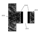
FIG. 9A shows an example in which the region corresponding to the source electrode and the drain electrode is the
A gray-tone mask described in
一方、TFT基板の製造方法の別の例として、例えば、特許文献2には、グレートーンマスクを用いる方法とレジストをリフローにより変形する方法の両方を組み合わせて用いたTFT基板の製造方法が開示されている。
以下、図10を用いて、特許文献2に記載された方法の一例を説明する。
図10(a)に示したように、ガラス基板101上にゲート電極102を形成し、ガラス基板101上に、ゲート電極102を覆ってゲート絶縁膜103を形成し、ゲート絶縁膜103上に、シリコン膜104,n+シリコン膜105,金属膜106を順次堆積して積層する。
次に、金属膜106上にポジ型のフォトレジストを塗布してレジスト膜107を形成し、図10(b)に示すように、レジスト膜107に対し、グレートーンマスク201を介して露光光を照射する。図11は、グレートーンマスクの平面図である。遮光部204は、ソース電極及びドレイン電極の対向部分であってチャネル部に隣接した領域に対応して形成され、ソース電極及びドレイン電極の残りの部分は半透光部203から形成され、ソース電極とドレイン電極の間のチャネル部は透光部205で形成されている。
On the other hand, as another example of a TFT substrate manufacturing method, for example,
Hereinafter, an example of the method described in
As shown in FIG. 10A, a
Next, a positive photoresist is applied on the
次に、露光後のポジ型のフォトレジストを現像すると、厚レジストパターン107a部分は、ほとんど溶解せずに残り、薄レジストパターン107b部分は、ある程度溶解し、他の部分は全て溶解して無くなる。この結果、図10(c)に示すように、膜厚の厚い厚レジストパターン107aと、膜厚の薄い薄レジストパターン107bが同時に形成できる。
次に、厚レジストパターン107aおよび薄レジストパターン107bをマスクとしてエッチングを行うことで、図10(d)に示すように、シリコン膜104上に、オーミックコンタクト層105a,105bおよびソース電極106a,ドレイン電極106bを形成する。
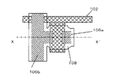
オーミックコンタクト層105a,105bを形成した後、加熱により、厚レジストパターン107aと薄レジストパターン107bとをリフローさせる。このことにより、有機樹脂である各レジストパターンは、シリコン膜104平面に広がり、オーミックコンタクト層105aとオーミックコンタクト層105bの間のシリコン膜104上では、厚レジストパターン107aと厚レジストパターン107bとがつながり、図10(e)及び図12の平面図に示すように、リフローレジストパターン108が形成される。尚、図10(e)は、図12のx−x断面を示している。
Next, when the positive photoresist after exposure is developed, the
Next, by performing etching using the
After the
つぎに、リフローレジストパターン108をマスクとしてシリコン層104をエッチング除去し、リフローレジストパターン108を除去することで、半導体島上に、オーミックコンタクト層105a,105bおよびソース電極106a,ドレイン電極106bが形成された状態が得られる(図示せず)。この後、パッシベーション膜を形成し、ソース電極106a,ドレイン電極106b上に各々コンタクトホールを形成し、これらコンタクトホール底部でソース電極106aに接続する画素電極、ドレイン電極106bに接続する端子部電極を形成する(図示せず)。
Next, the
次に、特許文献2に記載の他の例について図13を用いて説明する。
本例では、オーミックコンタクト層105a,105bおよびソース電極106a,ドレイン電極106bを形成した後、例えば酸素プラズマ雰囲気に曝すことで、各レジストパターンをプラズマ処理し、図13(a)に示すように薄レジストパターン107bを除去するようにした。
次に、厚レジストパターン107aを残した状態で、加熱により、これらをリフローさせる。このことにより、有機樹脂である各レジストパターンは、シリコン膜104平面に広がり、オーミックコンタクト層105aとオーミックコンタクト層105bの間のシリコン膜104上では、両側の厚レジストパターン107aが接触する。
この結果、図13(b)および図14の平面図に示すように、オーミックコンタクト層105aとオーミックコンタクト層105bとに挾まれたチャネルが形成される箇所を中心とした領域に、リフローレジストパターン109が形成される。リフローレジストパターン109は、ソース電極106a,ドレイン電極106bより幅広に形成される。尚、図13(b)は、図14のY−Y断面を示している。
Next, another example described in
In this example, after the
Next, with the
As a result, as shown in the plan views of FIG. 13B and FIG. 14, the
この後、リフローレジストパターン109および、リフローレジストパターン109に覆われていない領域のソース電極106a、ドレイン電極106bをマスクとしてシリコン層104をドライエッチングし、半導体島を形成する(図示せず)。
この後、前述した例と同様に、パッシベーション膜を形成し、ソース電極106a,ドレイン電極106b上に各々コンタクトホールを形成し、これらコンタクトホール底部でソース電極106aに接続する画素電極、ドレイン電極106bに接続する端子部電極を形成する(図示せず)。
特許文献2に記載された、ソース電極及びドレイン電極の対向部分を除く領域が半透光部となるグレートーンマスクを、従来例2と呼ぶ。
Thereafter, as in the example described above, a passivation film is formed, contact holes are formed on the
The gray-tone mask described in
上述の従来例2に記載されたような、ソース電極及びドレイン電極の対向部分を除く領域が半透光部となるグレートーンマスクは、半透光部が占める面積が広いため、マスクが使用される露光装置の解像度よりも小さい微細パターンにより半透光部を形成したのでは、広範囲での高精度の微細パターンが得られないと半透光部において均一な透過率分布が悪化してしまうという問題点がある。
一方、上記の微細パターンからなる半透光部の場合は、遮光部を形成する遮光性クロム膜を微細パターン状に形成することから、半透光部の形成と遮光部の形成とを1回のフォトリソ工程(描画、レジスト現像、エッチング)で行うことができるが、半透光部を半透光膜とした場合、半透光部の形成と遮光部の形成と、別々のフォトリソ工程を用いる必要がある。このように、2回描画を行う際には、1回目の描画とパターンずれが起きないようにアライメントをとって2回目の描画を行うが、アライメント精度には限界がありアライメントずれを完全になくすことは困難である。従って、半透光部を半透光膜とした場合、2回描画のアライメントずれ等の理由により、良好なパターンが得られなくなる場合があるという問題点があった。
As described in the above-described conventional example 2, the gray tone mask in which the region excluding the facing portion of the source electrode and the drain electrode is a semi-transparent portion has a large area occupied by the semi-transparent portion, and therefore the mask is used. If the semi-transmission part is formed with a fine pattern smaller than the resolution of the exposure apparatus, a uniform transmittance distribution in the semi-transmission part is deteriorated unless a high-precision fine pattern in a wide range is obtained. There is a problem.
On the other hand, in the case of the semi-transparent portion having the above-described fine pattern, the light-shielding chromium film for forming the light-shielding portion is formed in a fine pattern, so that the semi-transparent portion and the light-shielding portion are formed once. However, when the semi-translucent portion is a semi-transparent film, the formation of the semi-translucent portion and the formation of the light-shielding portion and separate photolithographic steps are used. There is a need. As described above, when performing the second drawing, the second drawing is performed by performing alignment so that the pattern deviation does not occur with the first drawing, but the alignment accuracy is limited and the alignment deviation is completely eliminated. It is difficult. Therefore, when the semi-transparent portion is a semi-transparent film, there is a problem that a good pattern may not be obtained due to misalignment of two-time drawing.
図15は、従来例2のグレートーンマスクについて、半透光部203と遮光部204とが、位置ずれを起こした例を示す平面図である。この例のように、半透光部がX方向左右に位置ずれを起こした場合、チャネル部に対応する透光部205の幅が設計値と変わってしまい、TFT基板の特性が変わってしまうという不具合が生じてしまう。このように、TFTで特に重要なチャネル部を精度よく形成することができるグレートーンマスクが得られない場合があるという問題点があった。
FIG. 15 is a plan view showing an example in which the
本発明は、上記事情を鑑みてなされたものであり、上記従来例2のグレートーンマスク、即ち、薄膜トランジスタ基板におけるソース電極及びドレイン電極に対応するパターンのソース電極及びドレイン電極の対向部分に形成された前記厚レジストパターン形成部と、ソース電極及びドレイン電極の厚レジストパターン形成部以外の部分に形成された前記薄レジストパターン形成部と、チャネル部に対応する部分を含む他の領域に形成された前記無レジスト領域形成部とを有し、少なくとも前記厚レジストパターン形成部によって形成された厚レジストパターンを変形する工程を有する薄膜トランジスタ基板の製造工程において使用されるグレートーンマスクとして、半透光部の透過率分布が良好で、かつチャネル部に対応するパターンのパターン精度が良好なグレートーンマスクを提供することを目的とする。
さらに、本発明は、上記従来例2のグレートーンマスク、即ち、薄膜トランジスタ基板におけるソース電極及びドレイン電極に対応するパターンのソース電極及びドレイン電極の対向部分に形成された前記厚レジストパターン形成部と、ソース電極及びドレイン電極の厚レジストパターン形成部以外の部分に形成された前記薄レジストパターン形成部と、チャネル部に対応する部分を含む他の領域に形成された前記無レジスト領域形成部とを有し、少なくとも前記厚レジストパターン形成部によって形成された厚レジストパターンを変形する工程を有する薄膜トランジスタ基板の製造工程において使用されるグレートーンマスクの製造方法として、半透光部の透過率分布が良好で、かつチャネル部に対応するパターンのパターン精度が良好なグレートーンマスクの製造方法を提供することを目的とする。
The present invention has been made in view of the above circumstances, and is formed on the gray tone mask of the above-described Conventional Example 2, that is, formed in a portion facing the source electrode and the drain electrode in a pattern corresponding to the source electrode and the drain electrode in the thin film transistor substrate. The thick resist pattern forming portion, the thin resist pattern forming portion formed in a portion other than the thick resist pattern forming portion of the source electrode and the drain electrode, and formed in another region including a portion corresponding to the channel portion. As a gray tone mask used in a manufacturing process of a thin film transistor substrate having a step of deforming at least the thick resist pattern formed by the thick resist pattern forming portion, the semi-transparent portion Pattern distribution corresponding to the channel part with good transmittance distribution Aims to have over down accurately to provide a good gray-tone mask.
Furthermore, the present invention relates to the gray-tone mask of the above-mentioned conventional example 2, that is, the thick resist pattern forming portion formed in a portion corresponding to the source electrode and the drain electrode of the pattern corresponding to the source electrode and the drain electrode in the thin film transistor substrate, The thin resist pattern forming portion formed in a portion other than the thick resist pattern forming portion of the source electrode and the drain electrode, and the non-resist region forming portion formed in another region including a portion corresponding to the channel portion. As a method for manufacturing a gray-tone mask used in a manufacturing process of a thin film transistor substrate having a process of deforming at least the thick resist pattern formed by the thick resist pattern forming part, the transmittance distribution of the semi-transparent part is good. And the pattern accuracy of the pattern corresponding to the channel part is good And to provide a method for producing laser-tone mask.
上記課題を解決するため、本発明は以下の構成を有する。
(構成1)被転写基板上に、厚レジストパターン、薄レジストパターン、及び無レジスト領域を形成するための厚レジストパターン形成部、薄レジストパターン形成部、及び無レジスト領域形成部を有し、前記薄レジストパターン形成部は半透光部からなり、厚レジストパターン及び無レジスト領域形成部は、それぞれ被転写基板上のレジストのポジ型かネガ型かに応じて決定された遮光部又は透光部からなるグレートーンマスクにおいて、前記グレートーンマスクは、薄膜トランジスタ基板におけるソース電極及びドレイン電極に対応するパターンのソース電極及びドレイン電極の対向部分に形成された前記厚レジストパターン形成部と、ソース電極及びドレイン電極の厚レジストパターン形成部以外の部分に形成された前記薄レジストパターン形成部と、チャネル部に対応する部分を含む他の領域に形成された前記無レジスト領域形成部とを有し、少なくとも前記厚レジストパターン形成部によって形成された厚レジストパターンを変形する工程を有する薄膜トランジスタ基板の製造工程において使用されるグレートーンマスクであって、前記半透光部は、半透光膜が形成され、前記遮光部は、遮光膜が形成され、前記厚レジストパターン形成部は、前記ソース電極及びドレイン電極の対向部分であって、少なくともチャネル部側に所望のマージン領域を空けて形成されてなることを特徴とするグレートーンマスクである。
In order to solve the above problems, the present invention has the following configuration.
(Configuration 1) A thick resist pattern, a thin resist pattern, and a thick resist pattern forming portion for forming a resist-free region on the substrate to be transferred, a thin resist pattern forming portion, and a resist-free region forming portion, The thin resist pattern forming part is composed of a semi-transparent part, and the thick resist pattern and the non-resist area forming part are respectively a light shielding part or a light transmitting part determined according to whether the resist on the transfer substrate is positive or negative. The gray tone mask comprises: the thick resist pattern forming portion formed on the opposing portion of the source electrode and the drain electrode of the pattern corresponding to the source electrode and the drain electrode in the thin film transistor substrate; and the source electrode and the drain The thin resist pattern formed in a portion other than the thick resist pattern forming portion of the electrode. And a step of deforming at least the thick resist pattern formed by the thick resist pattern forming portion, and a non-resist region forming portion formed in another region including a portion corresponding to the channel portion. A gray-tone mask used in a manufacturing process of a thin film transistor substrate having the semi-transparent portion, wherein the semi-transparent portion is formed with a semi-transparent film, the light-shielding portion is formed with a light-shielding film, and the thick resist pattern forming portion Is a gray-tone mask formed by forming a desired margin region at least on the channel portion side, which is a portion facing the source electrode and the drain electrode.
(構成2)前記遮光部は、少なくとも半透光膜と、その上に積層された遮光膜とからなることを特徴とする構成1に記載のグレートーンマスクである。
(構成3)前記遮光部は、少なくとも遮光膜と、その上に積層された半透光膜とからなることを特徴とする構成1に記載のグレートーンマスクである。
(Structure 2) The gray-tone mask according to
(Structure 3) The gray-tone mask according to
(構成4)被転写基板上に、厚レジストパターン、薄レジストパターン、及び無レジスト領域を形成するための厚レジストパターン形成部、薄レジストパターン形成部、及び無レジスト領域形成部を有し、前記薄レジストパターン形成部は半透光部からなり、厚レジストパターン及び無レジスト領域形成部は、それぞれ被転写基板上のレジストのポジ型かネガ型かに応じて決定された遮光部又は透光部からなるグレートーンマスクの製造方法において、前記グレートーンマスクは、薄膜トランジスタ基板におけるソース電極及びドレイン電極に対応するパターンのソース電極及びドレイン電極の対向部分に形成された前記厚レジストパターン形成部と、ソース電極及びドレイン電極の厚レジストパターン形成部以外の部分に形成された前記薄レジストパターン形成部と、チャネル部に対応する部分を含む他の領域に形成された前記無レジスト領域形成部とを有し、少なくとも前記厚レジストパターン形成部によって形成された厚レジストパターンを変形する工程を有する薄膜トランジスタ基板の製造工程において使用されるグレートーンマスクであって、透明基板上に、少なくとも半透光膜、遮光膜が積層されたマスクブランクを準備する工程と、遮光膜パターンを形成するための第1のレジスト膜に第1の描画パターンを描画、現像して第1のレジストパターンを形成し、該第1のレジストパターンをマスクとして遮光膜をエッチングする工程を含む遮光膜パターン形成工程と、半透光膜パターンを形成するための第2のレジスト膜に第2の描画パターンを描画、現像して第2のレジストパターンを形成し、該第2のレジストパターンをマスクとして半透光膜をエッチングする工程を含む半透光膜パターン形成工程とを有し、前記第1の描画パターンは、前記ソース電極及びドレイン電極の対向部分であって、少なくともチャネル部側に所望のマージン領域を空けた位置に対応する厚レジストパターン形成部を形成するためのパターンであり、前記第2の描画パターンは、前記ソース電極及びドレイン電極に対応するパターンであることを特徴とするグレートーンマスクの製造方法である。
(構成5)前記マスクブランクの半透光膜と遮光膜との間に、遮光膜をエッチングにより除去する際に半透光膜を保護するためのバッファー膜を設けることを特徴とする構成4に記載のグレートーンマスクの製造方法である。
(Configuration 4) A thick resist pattern, a thin resist pattern, and a thick resist pattern forming portion for forming a resist-free region on the substrate to be transferred, a thin resist pattern forming portion, and a resist-free region forming portion, The thin resist pattern forming part is composed of a semi-transparent part, and the thick resist pattern and the non-resist area forming part are respectively a light-shielding part or a light-transmitting part determined according to whether the resist on the transfer substrate is positive type or negative type. In the method of manufacturing a gray tone mask, the gray tone mask includes the thick resist pattern forming portion formed on the opposing portion of the source electrode and the drain electrode of the pattern corresponding to the source electrode and the drain electrode in the thin film transistor substrate, and the source The thin electrode formed on the electrode and the drain electrode other than the thick resist pattern forming portion. A step of deforming at least the thick resist pattern formed by the thick resist pattern forming portion, the resist pattern forming portion having a resist pattern forming portion formed in another region including a portion corresponding to the channel portion; A gray-tone mask used in a manufacturing process of a thin film transistor substrate having a step of preparing a mask blank in which at least a semi-transparent film and a light shielding film are laminated on a transparent substrate, and for forming a light shielding film pattern A light-shielding film pattern forming step including a step of drawing and developing a first drawing pattern on the first resist film to form a first resist pattern, and etching the light-shielding film using the first resist pattern as a mask; The second drawing pattern is drawn and developed on the second resist film for forming the semi-transparent film pattern. A semi-transparent film pattern forming step including a step of forming a resist pattern and etching the semi-transparent film using the second resist pattern as a mask, wherein the first drawing pattern includes the source electrode and the drain This is a pattern for forming a thick resist pattern forming portion corresponding to a position at which a desired margin region is opened at least on the channel portion side, which is an opposing portion of the electrode, and the second drawing pattern includes the source electrode and A method of manufacturing a gray-tone mask, wherein the pattern corresponds to a drain electrode.
(Structure 5) Structure 4 is characterized in that a buffer film is provided between the semi-transmissive film and the light-shielding film of the mask blank to protect the semi-transmissive film when the light-shielding film is removed by etching. It is a manufacturing method of the described gray-tone mask.
(構成6)被転写基板上に、厚レジストパターン、薄レジストパターン、及び無レジスト領域を形成するための厚レジストパターン形成部、薄レジストパターン形成部、及び無レジスト領域形成部を有し、前記薄レジストパターン形成部は半透光部からなり、厚レジストパターン及び無レジスト領域形成部は、それぞれ被転写基板上のレジストのポジ型かネガ型かに応じて決定された遮光部又は透光部からなるグレートーンマスクの製造方法において、前記グレートーンマスクは、薄膜トランジスタ基板におけるソース電極及びドレイン電極に対応するパターンのソース電極及びドレイン電極の対向部分に形成された前記厚レジストパターン形成部と、ソース電極及びドレイン電極の厚レジストパターン形成部以外の部分に形成された前記薄レジストパターン形成部と、チャネル部に対応する部分を含む他の領域に形成された前記無レジスト領域形成部とを有し、少なくとも前記厚レジストパターン形成部によって形成された厚レジストパターンを変形する工程を有する薄膜トランジスタ基板の製造工程において使用されるグレートーンマスクであって、透明基板上に、少なくとも、透過率の膜厚依存性を有する遮光膜が形成されたマスクブランクを準備する工程と、遮光膜パターンを形成するための第1のレジスト膜に第1の描画パターンを描画、現像して第1のレジストパターンを形成し、該第1のレジストパターンをマスクとして遮光膜をエッチングする工程を含む遮光部パターン形成工程と、半透光膜パターンを形成するための第2のレジスト膜に第2の描画パターンを描画、現像して第2のレジストパターンを形成し、該第2のレジストパターンをマスクとして遮光膜を所望の透過率となるような膜厚にエッチングする工程を含む半透光膜パターン形成工程とを有し、前記第1の描画パターンは、前記ソース電極及びドレイン電極の対向部分であって、少なくともチャネル部側に所望のマージン領域を空けた位置に対応する厚レジストパターン形成部を形成するためのパターンであり、前記第2の描画パターンは、前記ソース電極及びドレイン電極に対応するパターンであることを特徴とするグレートーンマスクの製造方法である。 (Structure 6) A thick resist pattern, a thin resist pattern, and a thick resist pattern forming portion for forming a resist-free region on the substrate to be transferred, a thin resist pattern forming portion, and a resist-free region forming portion, The thin resist pattern forming part is composed of a semi-transparent part, and the thick resist pattern and the non-resist area forming part are respectively a light-shielding part or a light-transmitting part determined according to whether the resist on the transfer substrate is positive type or negative type. In the method of manufacturing a gray tone mask, the gray tone mask includes the thick resist pattern forming portion formed on the opposing portion of the source electrode and the drain electrode of the pattern corresponding to the source electrode and the drain electrode in the thin film transistor substrate, and the source The thin electrode formed on the electrode and the drain electrode other than the thick resist pattern forming portion. A step of deforming at least the thick resist pattern formed by the thick resist pattern forming portion, the resist pattern forming portion having a resist pattern forming portion formed in another region including a portion corresponding to the channel portion; A step of preparing a mask blank in which a light-shielding film having at least a film thickness dependency of transmittance is formed on a transparent substrate, and a light-shielding film. A light shielding process including a step of drawing and developing a first drawing pattern on a first resist film for forming a pattern to form a first resist pattern, and etching the light shielding film using the first resist pattern as a mask. The second pattern is drawn on the second resist film for forming the partial pattern forming step and the semi-transparent film pattern. Developing a second resist pattern, and using the second resist pattern as a mask, a step of forming a translucent film pattern including a step of etching the light-shielding film to a film thickness that achieves a desired transmittance. And the first drawing pattern is a portion facing the source electrode and the drain electrode, and is for forming a thick resist pattern forming portion corresponding to a position where a desired margin region is opened at least on the channel portion side. The method of manufacturing a gray-tone mask, wherein the second drawing pattern is a pattern corresponding to the source electrode and the drain electrode.
(構成7)被転写基板上に、厚レジストパターン、薄レジストパターン、及び無レジスト領域を形成するための厚レジストパターン形成部、薄レジストパターン形成部、及び無レジスト領域形成部を有し、前記薄レジストパターン形成部は半透光部からなり、厚レジストパターン及び無レジスト領域形成部は、それぞれ被転写基板上のレジストのポジ型かネガ型かに応じて決定された遮光部又は透光部からなるグレートーンマスクの製造方法において、前記グレートーンマスクは、薄膜トランジスタ基板におけるソース電極及びドレイン電極に対応するパターンのソース電極及びドレイン電極の対向部分に形成された前記厚レジストパターン形成部と、ソース電極及びドレイン電極の厚レジストパターン形成部以外の部分に形成された前記薄レジストパターン形成部と、チャネル部に対応する部分を含む他の領域に形成された前記無レジスト領域形成部とを有し、少なくとも前記厚レジストパターン形成部によって形成された厚レジストパターンを変形する工程を有する薄膜トランジスタ基板の製造工程において使用されるグレートーンマスクであって、透明基板上に、少なくとも遮光膜が形成されたマスクブランクを準備する工程と、遮光膜パターンを形成するための第1のレジスト膜に第1の描画パターンを描画、現像して第1のレジストパターンを形成し、該第1のレジストパターンをマスクとして遮光膜をエッチングする工程を含む遮光部パターン形成工程と、次に、前記遮光部が形成された透明基板上に半透光膜を形成する工程と、次いで、半透光膜パターンを形成するために前記半透光膜上に形成した第2のレジスト膜に第2の描画パターンを描画、現像して第2のレジストパターンを形成し、該第2のレジストパターンをマスクとして半透光膜をエッチングする工程を含む半透光膜パターン形成工程とを有し、前記第1の描画パターンは、前記ソース電極及びドレイン電極の対向部分であって、少なくともチャネル部側に所望のマージン領域を空けた位置に対応する厚レジストパターン形成部を形成するためのパターンであり、前記第2の描画パターンは、前記ソース電極及びドレイン電極に対応するパターンであることを特徴とするグレートーンマスクの製造方法である。 (Structure 7) A thick resist pattern, a thin resist pattern, and a thick resist pattern forming portion for forming a non-resist region, a thin resist pattern forming portion, and a non-resist region forming portion on the transfer substrate, The thin resist pattern forming part is composed of a semi-transparent part, and the thick resist pattern and the non-resist area forming part are respectively a light-shielding part or a light-transmitting part determined according to whether the resist on the transfer substrate is positive type or negative type. In the method of manufacturing a gray tone mask, the gray tone mask includes the thick resist pattern forming portion formed on the opposing portion of the source electrode and the drain electrode of the pattern corresponding to the source electrode and the drain electrode in the thin film transistor substrate, and the source The thin electrode formed on the electrode and the drain electrode other than the thick resist pattern forming portion. A step of deforming at least the thick resist pattern formed by the thick resist pattern forming portion, the resist pattern forming portion having a resist pattern forming portion formed in another region including a portion corresponding to the channel portion; A gray-tone mask used in a manufacturing process of a thin film transistor substrate having: a step of preparing a mask blank having at least a light shielding film formed on a transparent substrate; and a first resist for forming a light shielding film pattern Forming a first resist pattern on the film by forming and developing a first resist pattern, and etching the light-shielding film using the first resist pattern as a mask; Forming a semi-transparent film on the transparent substrate on which the light-shielding portion is formed, and then forming a semi-transparent film pattern For this purpose, a second drawing pattern is drawn and developed on the second resist film formed on the semi-transparent film to form a second resist pattern, and the semi-transparent film is formed using the second resist pattern as a mask. A step of forming a translucent film pattern including a step of etching the first drawing pattern, wherein the first drawing pattern is a portion facing the source electrode and the drain electrode, and at least a desired margin region is provided on the channel portion side. A method for producing a gray-tone mask, wherein the second drawing pattern is a pattern corresponding to the source electrode and the drain electrode. It is.
本発明のグレートーンマスクによれば、薄膜トランジスタ基板におけるソース電極及びドレイン電極に対応するパターンのソース電極及びドレイン電極の対向部分に形成された前記厚レジストパターン形成部と、ソース電極及びドレイン電極の厚レジストパターン形成部以外の部分に形成された前記薄レジストパターン形成部と、チャネル部に対応する部分を含む他の領域に形成された前記無レジスト領域形成部とを有し、少なくとも前記厚レジストパターン形成部によって形成された厚レジストパターンを変形する工程を有する薄膜トランジスタ基板の製造工程において使用されるグレートーンマスクとして、半透光部が、半透光膜が形成されていることにより、半透光部の透過率分布が良好で、かつ半透光部を半透光膜とすることによって問題となる2回描画のアライメントずれによるチャネル部に対応するパターンのパターン精度の悪化の問題を、前記ソース電極及びドレイン電極の対向部分であって、少なくともチャネル部側に所望のマージン領域を空けた厚レジストパターン形成部とすることによって抑制された、グレートーンマスクを提供することができる。 According to the gray-tone mask of the present invention, the thick resist pattern forming portion formed on the opposing portion of the source electrode and the drain electrode of the pattern corresponding to the source electrode and the drain electrode in the thin film transistor substrate, and the thickness of the source electrode and the drain electrode The thin resist pattern forming portion formed in a portion other than the resist pattern forming portion, and the non-resist region forming portion formed in another region including a portion corresponding to the channel portion, and at least the thick resist pattern As a gray-tone mask used in a manufacturing process of a thin film transistor substrate having a step of deforming a thick resist pattern formed by a forming portion, a semi-transparent portion is formed by forming a semi-transparent film so that the semi-transparent film is formed. The transmittance distribution of the part is good and the semi-transparent part is a semi-transparent film. The problem of deterioration of the pattern accuracy of the pattern corresponding to the channel part due to misalignment of the two-time drawing, which is a problem, is that a desired margin region is provided at least on the channel part side, at a portion facing the source electrode and the drain electrode. It is possible to provide a gray-tone mask that is suppressed by forming a thick resist pattern forming portion.
さらに、本発明のグレートーンマスクの製造方法によれば、薄膜トランジスタ基板におけるソース電極及びドレイン電極に対応するパターンのソース電極及びドレイン電極の対向部分に形成された前記厚レジストパターン形成部と、ソース電極及びドレイン電極の厚レジストパターン形成部以外の部分に形成された前記薄レジストパターン形成部と、チャネル部に対応する部分を含む他の領域に形成された前記無レジスト領域形成部とを有し、少なくとも前記厚レジストパターン形成部によって形成された厚レジストパターンを変形する工程を有する薄膜トランジスタ基板の製造工程において使用されるグレートーンマスクの製造方法として、半透光部を半透光膜で形成することにより、半透光部の透過率分布が良好で、かつ半透光部を半透光膜とすることによって問題となる2回描画のアライメントずれによるチャネル部に対応するパターンのパターン精度の悪化の問題を、前記ソース電極及びドレイン電極の対向部分であって、少なくともチャネル部側に所望のマージン領域を空けた厚レジストパターン形成部を形成して遮光部とすることによって抑制することができる、グレートーンマスクの製造方法を提供することができる。 Furthermore, according to the method for manufacturing a gray-tone mask of the present invention, the thick resist pattern forming portion formed on the opposing portion of the source electrode and the drain electrode of the pattern corresponding to the source electrode and the drain electrode in the thin film transistor substrate, and the source electrode And the thin resist pattern forming portion formed in a portion other than the thick resist pattern forming portion of the drain electrode, and the non-resist region forming portion formed in another region including a portion corresponding to the channel portion, As a manufacturing method of a gray tone mask used in a manufacturing process of a thin film transistor substrate having a step of deforming at least the thick resist pattern formed by the thick resist pattern forming portion, a semi-transparent portion is formed of a semi-transparent film. Therefore, the transmittance distribution of the semi-translucent part is good and the semi-translucent part is semi-transparent. The problem of deterioration of the pattern accuracy of the pattern corresponding to the channel portion due to misalignment of the two-time drawing, which is a problem caused by forming a film, is a portion facing the source electrode and the drain electrode, and at least on the channel portion side. It is possible to provide a method for manufacturing a gray-tone mask, which can be suppressed by forming a thick resist pattern forming portion with a margin area as a light shielding portion.
以下、本発明を実施の形態により詳細に説明する。尚、以下の実施の形態においては、被転写基板上のレジストにポジ型レジストを用いることを前提に、厚レジストパターン形成部を遮光部、無レジスト領域形成部を透光部としたグレートーンマスクについて説明する。
(実施の形態1)
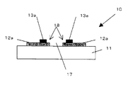
図1は、本発明の一実施の形態に係るグレートーンマスクの、TFT基板におけるソース電極及びドレイン電極付近のパターンを示す断面図であり、図2は、その平面図である。
図1及び図2に示されているように、実施の形態1では、石英等の透明基板11上に、ソース電極及びドレイン電極に対応する領域に形成された、半透光膜パターン12aと、ソース電極及びドレイン電極の対向部分に対応する領域に形成され、かつチャネル部に対応する透光部17側に、所望のマージン領域18を空けて前記半透光膜パターン12aの上に形成された遮光膜パターン13aを有する。即ち、遮光膜パターン13aが半透光膜パターン12aと積層された部分が遮光部、遮光部以外の半透光膜が形成された領域が半透光部、半透光膜12aも遮光膜13aも形成されていない領域が透光部である。
Hereinafter, the present invention will be described in detail by embodiments. In the following embodiments, assuming that a positive resist is used as a resist on the substrate to be transferred, a gray tone mask having a thick resist pattern forming portion as a light shielding portion and a non-resist region forming portion as a translucent portion. Will be described.
(Embodiment 1)
FIG. 1 is a cross-sectional view showing a pattern near a source electrode and a drain electrode on a TFT substrate of a gray-tone mask according to an embodiment of the present invention, and FIG. 2 is a plan view thereof.
As shown in FIGS. 1 and 2, in the first embodiment, a
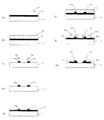
次に、上記グレートーンマスクを製造する方法について図3を用いて説明する。
本実施の形態で使用するマスクブランク14は、図3(a)に示すように、石英等からなる、主表面のサイズが450mm×550mmの大型透明基板11上に、半透光膜12及び遮光膜13を順次形成したものである。
ここで、遮光膜13の材質としては、薄膜で高い遮光性が得られるものが好ましく、例えばCr,Si,W,Al等が挙げられる。尚、遮光膜13は、表面又は表裏面に、例えば前記金属の酸化物からなる反射防止層を有するものであってもよい。また、半透光膜12の材質としては、薄膜で、透光部の透過率を100%とした場合に透過率50%程度の半透光性が得られるものが好ましく、例えばCr化合物(Crの酸化物、窒化物、酸窒化物、フッ化物など)、MoSi、Si,W,Al等が挙げられる。Si,W,Al等は、その膜厚によって高い遮光性も得られ、或いは半透光性も得られる材質である。また、形成されるマスクの遮光部は半透光膜12と遮光膜13の積層となるため、遮光膜単独では遮光性が足りなくても半透光膜と合わせた場合に遮光性が得られれば良い。なお、ここで透過率とは、グレートーンマスクを使用する例えば大型LCD用露光機の露光光の波長に対する透過率のことである。また、半透光膜の透過率は50%程度に限定される必要は全くない。半透光部の透過性をどの程度に設定するかは設計上の問題である。
Next, a method for manufacturing the gray tone mask will be described with reference to FIG.
As shown in FIG. 3A, the mask blank 14 used in the present embodiment is formed on a large
Here, the material of the
また、上記遮光膜13と半透光膜12の材質の組合せに関しては、互いの膜のエッチング特性が異なり、一方の膜のエッチング環境において他方の膜は耐性を有することが必要である。例えば、遮光膜13をCr,半透光膜12をMoSiで形成した場合、Cr遮光膜を塩素系ガスを用いてドライエッチング又は硝酸第2セリウムアンモニウムと過酸素塩を混合させて希釈したエッチング液を用いてウェットエッチングすると、下地のMoSi半透光膜との間では高いエッチング選択比が得られるので、MoSi半透光膜に殆どダメージを与えずにCr遮光膜だけをエッチングにより除去することが可能である。さらに、上記遮光膜13と半透光膜12は、基板上に成膜したときに密着性が良好であることが望ましい。
上記マスクブランク14は、透明基板11上に半透光膜12及び遮光膜13を順次成膜することで得られるが、成膜方法は、蒸着法、スパッタ法、CVD(化学的気相成長)法など、膜種に適した方法を適宜選択すればよい。また、膜厚に関しては、特に制約はないが、要は良好な遮光性或いは半透光性が得られるように最適化された膜厚で形成すればよい。
Further, regarding the combination of materials of the
The mask blank 14 can be obtained by sequentially forming the
次に、このマスクブランク上に例えば電子線或いはレーザ描画用のポジ型レジストを塗布し、ベーキングを行って、遮光膜パターンを形成するための第1のレジスト膜15を形成する(図3(b)参照)。次に、電子線描画機或いはレーザ描画機などを用いて描画を行う。描画データ(第1の描画データ)は、図1に示す、ソース電極とドレイン電極の対向部分に、チャネル部側に所望のマージン領域を空けた位置に対応する遮光膜パターン13aのパターンデータである。描画後、これを現像して、マスクブランク上に遮光部に対応する第1のレジストパターン15aを形成する(図3(c)参照)。尚、このマージン領域は、2回描画のアライメント精度を考慮して、想定されるアライメントずれよりも大きいチャネル部側からの幅とすることが好ましく、本実施の形態の場合は、0.1〜1μm程度幅のマージン領域とすることが好ましい。
Next, for example, a positive resist for electron beam or laser drawing is applied on the mask blank and baked to form a first resist
次に、形成されたレジストパターン15aをマスクとして、遮光膜13をドライエッチングして、遮光部に対応する遮光膜パターン13aを形成する(図3(c)参照)。遮光膜13がCr系材料からなる場合、塩素ガスを用いたドライエッチングを用いることが出来る。遮光部に対応する領域以外は、遮光膜13のエッチングにより下地の半透光膜12が露出した状態である。残存するレジストパターン15aは、酸素によるアッシング或いは濃硫酸などを用いて除去する(図3(d)参照)。
次に、再び全面に前記レジストを塗布して第2のレジスト膜16を形成する(図3(e)参照)。そして、2回目の描画を行う。この時の描画データ(第2の描画データ)は、図1に示すソース電極とドレイン電極に対応するパターンデータである。描画後、これを現像して、半透光膜パターンを形成するためのレジストパターン16aを形成する(図3(f)参照)。
Next, using the formed resist pattern 15a as a mask, the
Next, the resist is applied again on the entire surface to form a second resist film 16 (see FIG. 3E). Then, the second drawing is performed. The drawing data (second drawing data) at this time is pattern data corresponding to the source electrode and the drain electrode shown in FIG. After drawing, this is developed to form a resist
尚、本実施の形態のグレートーンマスクを用いたTFT基板製造工程においては、従来例2のグレートーンマスクと同様、ゲート電極上にソース電極及びドレイン電極を所定の間隔で形成するため、ゲート電極とソース及びドレイン電極のアライメントをとる必要があるため、ゲート電極とのアライメントに関係するマーク(露光の際の位置合わせマーク、位置精度確認用マーク等)をマスク上に設ける必要がある。その場合、ソース電極とドレイン電極に挟まれたチャネル部をゲート電極とが正確に位置合わせされることが重要であることから、ソース電極とドレイン電極の最もチャネル部側に形成される薄膜パターンと相関のとれたマークを、フォトマスクのパターン領域外に設けることが好ましい。本発明では、ソース電極とドレイン電極の最もチャネル部側に形成される薄膜パターンは、半透光膜パターンである。従って、本実施の形態においては、前記工程において、半透光膜パターンを形成するための描画データ(第2の描画データ)に、ゲート電極とのアライメントに関係するマークを含め、半透光膜パターンの形成と同じにマークの形成も行い、以降の工程において、半透光膜パターンと同様に、半透光膜により形成されたマークパターンを形成することができる。 In the TFT substrate manufacturing process using the gray-tone mask of the present embodiment, the source electrode and the drain electrode are formed on the gate electrode at a predetermined interval similarly to the gray-tone mask of Conventional Example 2, so that the gate electrode Since the source and drain electrodes need to be aligned, marks related to the alignment with the gate electrode (positioning marks for exposure, marks for checking position accuracy, etc.) must be provided on the mask. In that case, since it is important that the channel portion sandwiched between the source electrode and the drain electrode is accurately aligned with the gate electrode, the thin film pattern formed closest to the channel portion of the source electrode and the drain electrode It is preferable to provide a correlated mark outside the pattern region of the photomask. In the present invention, the thin film pattern formed closest to the channel portion of the source electrode and the drain electrode is a semi-transparent film pattern. Therefore, in the present embodiment, in the above process, the drawing data (second drawing data) for forming the semi-transparent film pattern includes the mark related to the alignment with the gate electrode, so that the semi-transmissive film A mark is also formed in the same manner as the pattern formation, and a mark pattern formed of a semi-transparent film can be formed in the subsequent steps in the same manner as the semi-transparent film pattern.
次に、形成されたレジストパターン16aをマスクとして、透光部となる領域の半透光膜12をエッチングにより除去する。これにより、半透光部は透光部と画され、半透光部及び透光部が形成される(図3(g)参照)。そして、残存するレジストパターンは酸素アッシング等を用いて除去する(図3(h)参照)。
以上のようにして本実施の形態の図1に示すグレートーンマスク10が出来上がる。
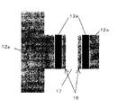
図4は、上記方法において、第1の描画パターンによる描画と、第2の描画パターンによる描画とが、アライメントずれを起こしたケースを想定した例であり、図4(a)は第1の描画パターンに対して第2の描画パターンがX方向左側に、図4(b)は第1の描画パターンに対して第2の描画パターンがX方向右側にずれた例である。これらの図に示されるように、本実施の形態におけるグレートーンマスクでは、チャネル部側にマージン領域を設けて遮光膜パターン13aを形成しているため、アライメントずれが発生してもチャネル部に対応するパターン寸法精度を悪化させることがない。
従って、本実施の態様によれば、TFT特性上重要なパターンを高精度で形成できるので、高品質のグレートーンマスクを提供することができる。
Next, by using the formed resist
As described above, the
FIG. 4 is an example assuming a case in which the drawing by the first drawing pattern and the drawing by the second drawing pattern cause misalignment in the above method, and FIG. 4A shows the first drawing. The second drawing pattern is shifted to the left in the X direction with respect to the pattern, and FIG. 4B is an example in which the second drawing pattern is shifted to the right in the X direction with respect to the first drawing pattern. As shown in these drawings, in the gray-tone mask according to the present embodiment, since the light
Therefore, according to this embodiment, a pattern important for TFT characteristics can be formed with high accuracy, and a high-quality gray-tone mask can be provided.
尚、本発明におけるグレートーンマスクの遮光部は、従来例2の製造方法に用いられるため、遮光部によって形成されたレジストパターンは、リフローされてしまうため、遮光部の位置が、従来例2のグレートーンマスクにおける位置と多少異なっても何ら問題とならない。
尚、本実施の形態において、使用するマスクブランクは、半透光膜12と遮光膜13の間にバッファー膜を形成したものであってもよい。すなわち、半透光膜12と遮光膜13との間に、エッチングストッパーとしての機能を有するバッファー膜を設けることで、1回目のフォトリソ工程において、レジストパターンの形成されていない領域の遮光膜をエッチングにより除去する際に、下層の半透光膜の膜減りなどのダメージを防止することができる。このようにバッファー膜を設けているので、遮光膜13及び半透光膜12は、エッチング特性が似かよった材質、例えば同一材料の膜や主成分が同じ材料の膜等で構成することが可能である。なお、バッファー膜の材質は、遮光膜13をエッチングする環境に耐性を有する材質から選択される。また、半透光部におけるバッファー膜を除去する必要がある場合には、ドライエッチング等の方法で下地の半透光膜12にダメージを与えずに除去できる材質であることも要求される。バッファー膜として例えばSiO2又はSOG(Spin On Glass)等を用いることが出来る。これらの材質は、遮光膜をCr系材料で構成する場合、遮光膜との間で高いエッチング選択比を取ることが出来る。また、これらの材質は透過性が良好であり、半透光部に介在してもその透過特性を損わないため除去しないでおくことも可能である。
In addition, since the light-shielding part of the gray tone mask in this invention is used for the manufacturing method of the prior art example 2, the resist pattern formed by the light-shielding part will be reflowed. There is no problem even if it is slightly different from the position in the gray tone mask.
In the present embodiment, the mask blank to be used may be one in which a buffer film is formed between the
さらに、マスクブランクとして、半透光膜と遮光膜が積層されたものを用いるのではなく、透過率の膜厚依存性を有する遮光膜が形成されたものを用い、遮光膜をエッチングして半透光膜を露出させる工程(図3(c)参照)として、遮光膜を所望の透過率となるような膜厚にエッチングする工程に置き換えることもできる。 Further, as a mask blank, a mask blank having a light-shielding film having a film thickness dependency is used instead of a semi-transparent film and a light-shielding film laminated. The step of exposing the light-transmitting film (see FIG. 3C) can be replaced with a step of etching the light-shielding film to a film thickness that achieves a desired transmittance.
(実施の形態2)
実施の形態2は、実施の形態1と同様のグレートーンマスクを、実施の形態1と異なる方法で製造した例である。
以下、図5を用いてその方法を説明する。
実施の形態1で用いたマスクブランク14を用意する(図5(a)参照)。
次に、マスクブランク14上に例えば電子線或いはレーザ描画用のポジ型レジストを塗布し、ベーキングを行って、半透光膜パターンを形成するためのレジスト膜16を形成する(図5(b)参照)。次に、電子線描画機或いはレーザ描画機などを用いて描画を行う。描画データ(第1の描画データ)は、図1に示す、ソース電極とドレイン電極に対応するパターンデータである。描画後、これを現像して、マスクブランク上にレジストパターン16aを形成する(図5(c)参照)。
(Embodiment 2)
The second embodiment is an example in which the same gray-tone mask as that of the first embodiment is manufactured by a method different from that of the first embodiment.
The method will be described below with reference to FIG.
The mask blank 14 used in the first embodiment is prepared (see FIG. 5A).
Next, for example, a positive resist for electron beam or laser drawing is applied on the mask blank 14 and baked to form a resist
尚、ゲート電極とのアライメントに関係するマークの形成については、前記工程において、半透光膜パターンを形成するための描画データ(第1の描画データ)に、ゲート電極とのアライメントに関係するマークを含め、次に続く遮光膜のエッチング及び半透光膜のエッチングにおいて、マークパターンを形成することができる。尚、マークパターンを形成する半透光膜上の遮光膜は、後記する遮光膜パターンを形成する工程において除去せずに残すことによって、半透光膜からなるマークよりも検出感度が高くなるため好ましい。
次に、形成されたレジストパターン16aをマスクとして、遮光膜13をエッチングして、引続き、半透光膜12をエッチングする(図5(d)参照)。残存するレジストパターン16aは、酸素によるアッシング或いは濃硫酸などを用いて除去する。
As for the formation of the mark related to the alignment with the gate electrode, the mark related to the alignment with the gate electrode is added to the drawing data (first drawing data) for forming the semi-transparent film pattern in the above process. In the subsequent etching of the light shielding film and the semi-transparent film, the mark pattern can be formed. In addition, since the light shielding film on the semi-transparent film forming the mark pattern is left without being removed in the process of forming the light shielding film pattern described later, the detection sensitivity becomes higher than the mark made of the semi-transparent film. preferable.
Next, the
次に、再び全面に前記レジストを塗布してレジスト膜15を形成する(図5(e)参照)。そして、2回目の描画を行う。この時の描画データ(第2の描画データ)は、ソース電極とドレイン電極の対向部分に、チャネル部側に所望のマージン領域を空けた位置に対応する遮光膜パターン13aのパターンデータである。描画後、これを現像して、遮光膜パターンを形成するためのレジストパターン15bを形成する(図5(f)参照)。尚、このマージン領域の幅は、実施の形態1と同様である。
次に、形成されたレジストパターン15bをマスクとして、露出した半透光膜上の遮光膜をドライエッチングにより除去する。これにより、遮光部は半透光部と画され、半透光部及び遮光部が形成される(図5(g)参照)。そして、残存するレジストパターンは酸素アッシング等を用いて除去する(図5(h)参照)。
本実施の形態においても、実施の形態1同様に、TFT特性上重要なパターンを高精度で形成できるので、高品質のグレートーンマスクを提供することができる。
Next, the resist is applied again on the entire surface to form a resist film 15 (see FIG. 5E). Then, the second drawing is performed. The drawing data (second drawing data) at this time is pattern data of the light-shielding
Next, using the formed resist pattern 15b as a mask, the exposed light shielding film on the semi-transparent film is removed by dry etching. Thereby, the light shielding part is defined as a semi-translucent part, and a semi-transparent part and a light shielding part are formed (see FIG. 5G). The remaining resist pattern is removed using oxygen ashing or the like (see FIG. 5H).
Also in the present embodiment, a pattern important for TFT characteristics can be formed with high accuracy as in the first embodiment, and thus a high-quality gray-tone mask can be provided.
尚、本実施の形態においても、実施の形態1同様に、半透光膜12と遮光膜13の間にバッファー膜を形成したマスクブランクを用いることもできる。
さらに、マスクブランクとして、半透光膜と遮光膜が積層されたものを用いるのではなく、透過率の膜厚依存性を有する遮光膜が形成されたものを用い、遮光膜をエッチングして半透光膜を露出させる工程(図5(c)参照)として、遮光膜を所望の透過率となるような膜厚にエッチングする工程に置き換えることもできる。
In the present embodiment, a mask blank in which a buffer film is formed between the
Further, as a mask blank, a mask blank having a light-shielding film having a film thickness dependency is used instead of a semi-transparent film and a light-shielding film laminated. The step of exposing the light-transmitting film (see FIG. 5C) can be replaced with a step of etching the light-shielding film to a film thickness that achieves a desired transmittance.
(実施の形態3)
実施の形態3は、実施の形態1のグレートーンマスクが半透光膜パターン12a上に遮光膜パターン13aが形成され、遮光部が、半透光膜とその上の遮光膜により形成されているのに対し、図6に示すように、遮光膜パターン13a上に半透光膜パターン12aが形成され、遮光部が、遮光膜とその上の半透光膜により形成されているグレートーンマスク20である。尚、本実施の形態のグレートーンマスク20の平面図は、遮光部において遮光膜パターン13aと半透光膜パターン12aの上下が逆となる以外は図2と同様であるため、省略する。
以下、図7を用いて、本実施の形態に係るグレートーンマスク20の製造方法を説明する。
(Embodiment 3)
In the third embodiment, the gray-tone mask of the first embodiment has the light-shielding
Hereinafter, the manufacturing method of the
本実施の形態では、まず、図7(a)に示すように、実施の形態1と同様の透明基板11上に、遮光膜13を形成したマスクブランク24を用いる。
このマスクブランク上に、例えばレーザ又は電子線描画用のポジ型レジストを塗布し、ベーキングを行って、遮光膜パターンを形成するための第1のレジスト膜15を形成する(図7(b)参照)。次に、電子線描画機或いはレーザ描画機などを用いて描画を行う。描画データ(第1の描画データ)は、図2に示す、ソース電極とドレイン電極の対向部分に、チャネル部側に所望のマージン領域を空けた位置に対応する遮光部13aのパターンデータである。描画後、これを現像して、マスクブランク上に遮光部に対応する第1のレジストパターン15aを形成する。尚、このマージン領域の幅は、実施の形態1と同様である。
In the present embodiment, first, as shown in FIG. 7A, a mask blank 24 in which a
On the mask blank, for example, a positive resist for laser or electron beam drawing is applied and baked to form a first resist
次に、形成された第1のレジストパターン15aをマスクとして、遮光膜13をウェット又はドライエッチングして、遮光部に対応するパターン13aを形成する(図7(c)参照)。遮光膜13がCr系材料からなる場合、ウェットエッチングには、例えば硝酸第2セリウムアンモニウムと過酸素塩を混合させて希釈したエッチング液等を用いることが出来、ドライエッチングには、Cl2+O2等の塩素系ガスを含むドライエッチングガスを用いることができる。残存するレジストパターン15aは、酸素によるアッシング或いは濃硫酸などを用いて除去する(図7(d)参照)。
次に、全面に、半透光膜12を形成する(図7(e)参照)。次に、半透光膜12上にレジストを塗布して半透光膜パターンを形成するための第2のレジスト膜16を形成する(図7(f)参照)。そして、2回目の描画を行う。この時の描画データ(第2の描画データ)は、図1に示すソース電極とドレイン電極に対応するパターンデータである。描画後、これを現像して、少なくとも半透光部に対応する第2のレジストパターン16aを形成する(図7(g)参照)。
Next, using the formed first resist pattern 15a as a mask, the
Next, a
尚、ゲート電極とのアライメントに関係するマークの形成については、前記工程において、半透光膜パターンを形成するための描画データ(第2の描画データ)に、ゲート電極とのアライメントに関係するマークを含め、半透光膜パターンの形成と同時にマークの形成も行い、以降の工程において、半透光膜パターンと同様に、半透光膜により形成されたマークパターンを形成することができる。
次に、形成された第2のレジストパターン16aをマスクとして、透光部となる領域の半透光膜12をウェット又はドライエッチングにより除去する。これにより、半透光部は透光部と画され、半透光部及び透光部が形成される。なお、残存するレジストパターンは酸素アッシング等を用いて除去する(図7(h)参照)。
本実施の形態においても、実施の形態1同様に、TFT特性上重要なパターンを高精度で形成できるので、高品質のグレートーンマスクを提供することができる。
In addition, regarding the formation of the mark related to the alignment with the gate electrode, the mark related to the alignment with the gate electrode is added to the drawing data (second drawing data) for forming the semi-transparent film pattern in the above process. In addition, the mark is also formed simultaneously with the formation of the semi-transparent film pattern. In the subsequent steps, the mark pattern formed of the semi-transparent film can be formed in the same manner as the semi-transparent film pattern.
Next, using the formed second resist
Also in the present embodiment, a pattern important for TFT characteristics can be formed with high accuracy as in the first embodiment, and thus a high-quality gray-tone mask can be provided.
(実施の形態4)
実施の形態4では、図8に示すように、Y方向のアライメントずれに対しても考慮し、遮光部のY方向側の透光部との境界部においてもマージン領域19を設けた例である。このマージン領域19の幅は、実施の形態1におけるチャネル部側のマージン領域18の幅と同様である。このような構成にすることによって、Y方向にアライメントずれが生じた場合であっても、遮光膜が、ソース電極及びドレイン電極の設計パターンよりはみ出てしまうことも防止することができる。
(Embodiment 4)
In the fourth embodiment, as shown in FIG. 8, the
10 グレートーンマスク
11 透明基板
12 半透光膜
12a 半透光膜パターン
13 遮光膜
13a 遮光膜パターン
14 マスクブランク
15 第1のレジスト膜
16 第2のレジスト膜
10
Claims (7)
前記グレートーンマスクは、薄膜トランジスタ基板におけるソース電極及びドレイン電極に対応するパターンのソース電極及びドレイン電極の対向部分に形成された前記厚レジストパターン形成部と、ソース電極及びドレイン電極の厚レジストパターン形成部以外の部分に形成された前記薄レジストパターン形成部と、チャネル部に対応する部分を含む他の領域に形成された前記無レジスト領域形成部とを有し、少なくとも前記厚レジストパターン形成部によって形成された厚レジストパターンを変形する工程を有する薄膜トランジスタ基板の製造工程において使用されるグレートーンマスクであって、
前記半透光部は、半透光膜が形成され、前記遮光部は、遮光膜が形成され、前記厚レジストパターン形成部は、前記ソース電極及びドレイン電極の対向部分であって、少なくともチャネル部側に所望のマージン領域を空けて形成されてなることを特徴とするグレートーンマスク。 Forming a thin resist pattern, a thin resist pattern, and a thick resist pattern forming portion for forming a non-resist region, a thin resist pattern forming portion, and a non-resist region forming portion on the transfer substrate; The part is composed of a semi-transparent part, and the thick resist pattern and the non-resist area forming part are gray tones composed of a light-shielding part or a light-transmitting part determined according to whether the resist on the transfer substrate is positive or negative, respectively. In the mask
The gray tone mask includes the thick resist pattern forming portion formed in a portion corresponding to the source electrode and the drain electrode in a pattern corresponding to the source electrode and the drain electrode in the thin film transistor substrate, and the thick resist pattern forming portion of the source electrode and the drain electrode. The thin resist pattern forming portion formed in a portion other than the portion and the non-resist region forming portion formed in another region including the portion corresponding to the channel portion, and formed by at least the thick resist pattern forming portion A gray-tone mask used in a manufacturing process of a thin film transistor substrate having a step of deforming a thick resist pattern,
The semi-transparent portion is formed with a semi-transparent film, the light-shielding portion is formed with a light-shielding film, and the thick resist pattern forming portion is a portion facing the source electrode and the drain electrode, and at least a channel portion A gray-tone mask, which is formed with a desired margin area on the side.
前記グレートーンマスクは、薄膜トランジスタ基板におけるソース電極及びドレイン電極に対応するパターンのソース電極及びドレイン電極の対向部分に形成された前記厚レジストパターン形成部と、ソース電極及びドレイン電極の厚レジストパターン形成部以外の部分に形成された前記薄レジストパターン形成部と、チャネル部に対応する部分を含む他の領域に形成された前記無レジスト領域形成部とを有し、少なくとも前記厚レジストパターン形成部によって形成された厚レジストパターンを変形する工程を有する薄膜トランジスタ基板の製造工程において使用されるグレートーンマスクであって、
透明基板上に、少なくとも半透光膜、遮光膜が積層されたマスクブランクを準備する工程と、
遮光膜パターンを形成するための第1のレジスト膜に第1の描画パターンを描画、現像して第1のレジストパターンを形成し、該第1のレジストパターンをマスクとして遮光膜をエッチングする工程を含む遮光膜パターン形成工程と、
半透光膜パターンを形成するための第2のレジスト膜に第2の描画パターンを描画、現像して第2のレジストパターンを形成し、該第2のレジストパターンをマスクとして半透光膜をエッチングする工程を含む半透光膜パターン形成工程と
を有し、
前記第1の描画パターンは、前記ソース電極及びドレイン電極の対向部分であって、少なくともチャネル部側に所望のマージン領域を空けた位置に対応する厚レジストパターン形成部を形成するためのパターンであり、前記第2の描画パターンは、前記ソース電極及びドレイン電極に対応するパターンであることを特徴とするグレートーンマスクの製造方法。 Forming a thin resist pattern, a thin resist pattern, and a thick resist pattern forming portion for forming a non-resist region, a thin resist pattern forming portion, and a non-resist region forming portion on the transfer substrate; The part is composed of a semi-transparent part, and the thick resist pattern and the non-resist area forming part are gray tones composed of a light-shielding part or a light-transmitting part determined according to whether the resist on the transfer substrate is positive or negative, respectively. In the mask manufacturing method,
The gray tone mask includes the thick resist pattern forming portion formed in a portion corresponding to the source electrode and the drain electrode in a pattern corresponding to the source electrode and the drain electrode in the thin film transistor substrate, and the thick resist pattern forming portion of the source electrode and the drain electrode. The thin resist pattern forming portion formed in a portion other than the portion and the non-resist region forming portion formed in another region including the portion corresponding to the channel portion, and formed by at least the thick resist pattern forming portion A gray-tone mask used in a manufacturing process of a thin film transistor substrate having a step of deforming a thick resist pattern,
Preparing a mask blank in which at least a semi-transparent film and a light-shielding film are laminated on a transparent substrate;
A step of drawing and developing a first drawing pattern on a first resist film for forming a light shielding film pattern to form a first resist pattern, and etching the light shielding film using the first resist pattern as a mask. Including a light shielding film pattern forming step,
A second drawing pattern is drawn and developed on the second resist film for forming the semi-transparent film pattern to form a second resist pattern, and the semi-transparent film is formed using the second resist pattern as a mask. A semi-transparent film pattern forming step including a step of etching, and
The first drawing pattern is a pattern for forming a thick resist pattern forming portion corresponding to a position where a desired margin region is opened at least on the channel portion side, which is a portion facing the source electrode and the drain electrode. The method of manufacturing a gray-tone mask, wherein the second drawing pattern is a pattern corresponding to the source electrode and the drain electrode.
前記グレートーンマスクは、薄膜トランジスタ基板におけるソース電極及びドレイン電極に対応するパターンのソース電極及びドレイン電極の対向部分に形成された前記厚レジストパターン形成部と、ソース電極及びドレイン電極の厚レジストパターン形成部以外の部分に形成された前記薄レジストパターン形成部と、チャネル部に対応する部分を含む他の領域に形成された前記無レジスト領域形成部とを有し、少なくとも前記厚レジストパターン形成部によって形成された厚レジストパターンを変形する工程を有する薄膜トランジスタ基板の製造工程において使用されるグレートーンマスクであって、
透明基板上に、少なくとも、透過率の膜厚依存性を有する遮光膜が形成されたマスクブランクを準備する工程と、
遮光膜パターンを形成するための第1のレジスト膜に第1の描画パターンを描画、現像して第1のレジストパターンを形成し、該第1のレジストパターンをマスクとして遮光膜をエッチングする工程を含む遮光部パターン形成工程と、
半透光膜パターンを形成するための第2のレジスト膜に第2の描画パターンを描画、現像して第2のレジストパターンを形成し、該第2のレジストパターンをマスクとして遮光膜を所望の透過率となるような膜厚にエッチングする工程を含む半透光膜パターン形成工程と
を有し、
前記第1の描画パターンは、前記ソース電極及びドレイン電極の対向部分であって、少なくともチャネル部側に所望のマージン領域を空けた位置に対応する厚レジストパターン形成部を形成するためのパターンであり、前記第2の描画パターンは、前記ソース電極及びドレイン電極に対応するパターンであることを特徴とするグレートーンマスクの製造方法。 Forming a thin resist pattern, a thin resist pattern, and a thick resist pattern forming portion for forming a non-resist region, a thin resist pattern forming portion, and a non-resist region forming portion on the transfer substrate; The part is composed of a semi-transparent part, and the thick resist pattern and the non-resist area forming part are gray tones composed of a light-shielding part or a light-transmitting part determined according to whether the resist on the transfer substrate is positive or negative, respectively. In the mask manufacturing method,
The gray tone mask includes the thick resist pattern forming portion formed in a portion corresponding to the source electrode and the drain electrode in a pattern corresponding to the source electrode and the drain electrode in the thin film transistor substrate, and the thick resist pattern forming portion of the source electrode and the drain electrode. The thin resist pattern forming portion formed in a portion other than the portion and the non-resist region forming portion formed in another region including the portion corresponding to the channel portion, and formed by at least the thick resist pattern forming portion A gray-tone mask used in a manufacturing process of a thin film transistor substrate having a step of deforming a thick resist pattern,
On the transparent substrate, at least a step of preparing a mask blank in which a light shielding film having a film thickness dependency of transmittance is formed;
A step of drawing and developing a first drawing pattern on a first resist film for forming a light shielding film pattern to form a first resist pattern, and etching the light shielding film using the first resist pattern as a mask. Including a light shielding part pattern forming step,
A second drawing pattern is drawn and developed on the second resist film for forming the semi-transparent film pattern to form a second resist pattern, and a desired light shielding film is formed using the second resist pattern as a mask. A semi-transparent film pattern forming step including a step of etching to a film thickness that provides transmittance,
The first drawing pattern is a pattern for forming a thick resist pattern forming portion corresponding to a position where a desired margin region is opened at least on the channel portion side, which is a portion facing the source electrode and the drain electrode. The method of manufacturing a gray-tone mask, wherein the second drawing pattern is a pattern corresponding to the source electrode and the drain electrode.
前記グレートーンマスクは、薄膜トランジスタ基板におけるソース電極及びドレイン電極に対応するパターンのソース電極及びドレイン電極の対向部分に形成された前記厚レジストパターン形成部と、ソース電極及びドレイン電極の厚レジストパターン形成部以外の部分に形成された前記薄レジストパターン形成部と、チャネル部に対応する部分を含む他の領域に形成された前記無レジスト領域形成部とを有し、少なくとも前記厚レジストパターン形成部によって形成された厚レジストパターンを変形する工程を有する薄膜トランジスタ基板の製造工程において使用されるグレートーンマスクであって、
透明基板上に、少なくとも遮光膜が形成されたマスクブランクを準備する工程と、
遮光膜パターンを形成するための第1のレジスト膜に第1の描画パターンを描画、現像して第1のレジストパターンを形成し、該第1のレジストパターンをマスクとして遮光膜をエッチングする工程を含む遮光部パターン形成工程と、
次に、前記遮光部が形成された透明基板上に半透光膜を形成する工程と、
次いで、半透光膜パターンを形成するために前記半透光膜上に形成した第2のレジスト膜に第2の描画パターンを描画、現像して第2のレジストパターンを形成し、該第2のレジストパターンをマスクとして半透光膜をエッチングする工程を含む半透光膜パターン形成工程と
を有し、
前記第1の描画パターンは、前記ソース電極及びドレイン電極の対向部分であって、少なくともチャネル部側に所望のマージン領域を空けた位置に対応する厚レジストパターン形成部を形成するためのパターンであり、前記第2の描画パターンは、前記ソース電極及びドレイン電極に対応するパターンであることを特徴とするグレートーンマスクの製造方法。 Forming a thin resist pattern, a thin resist pattern, and a thick resist pattern forming portion for forming a non-resist region, a thin resist pattern forming portion, and a non-resist region forming portion on the transfer substrate; The part is composed of a semi-transparent part, and the thick resist pattern and the non-resist area forming part are gray tones composed of a light-shielding part or a light-transmitting part determined according to whether the resist on the transfer substrate is positive or negative, respectively. In the mask manufacturing method,
The gray tone mask includes the thick resist pattern forming portion formed in a portion corresponding to the source electrode and the drain electrode in a pattern corresponding to the source electrode and the drain electrode in the thin film transistor substrate, and the thick resist pattern forming portion of the source electrode and the drain electrode. The thin resist pattern forming portion formed in a portion other than the portion and the non-resist region forming portion formed in another region including the portion corresponding to the channel portion, and formed by at least the thick resist pattern forming portion A gray-tone mask used in a manufacturing process of a thin film transistor substrate having a step of deforming a thick resist pattern,
Preparing a mask blank having at least a light shielding film formed on a transparent substrate; and
A step of drawing and developing a first drawing pattern on a first resist film for forming a light shielding film pattern to form a first resist pattern, and etching the light shielding film using the first resist pattern as a mask. Including a light shielding part pattern forming step,
Next, a step of forming a semi-transparent film on the transparent substrate on which the light shielding portion is formed,
Next, a second drawing pattern is drawn and developed on the second resist film formed on the semi-transparent film in order to form a semi-transparent film pattern, thereby forming the second resist pattern. A semi-transparent film pattern forming step including a step of etching the semi-transparent film using the resist pattern as a mask,
The first drawing pattern is a pattern for forming a thick resist pattern forming portion corresponding to a position where a desired margin region is opened at least on the channel portion side, which is a portion facing the source electrode and the drain electrode. The method of manufacturing a gray-tone mask, wherein the second drawing pattern is a pattern corresponding to the source electrode and the drain electrode.
Priority Applications (5)
| Application Number | Priority Date | Filing Date | Title |
|---|---|---|---|
| JP2004205306A JP2006030319A (en) | 2004-07-12 | 2004-07-12 | Gray tone mask and method for manufacturing gray tone mask |
| TW094123347A TW200608579A (en) | 2004-07-12 | 2005-07-11 | Gray tone mask and method for manufacturing the same |
| KR1020050062864A KR100965181B1 (en) | 2004-07-12 | 2005-07-12 | Gray tone mask and method for manufacturing the same |
| CN200910179767A CN101673049A (en) | 2004-07-12 | 2005-07-12 | Gray tone mask and method for manufacturing gray tone mask |
| CNB2005100840683A CN100562803C (en) | 2004-07-12 | 2005-07-12 | Gray mask and gray tone mask manufacturing method |
Applications Claiming Priority (1)
| Application Number | Priority Date | Filing Date | Title |
|---|---|---|---|
| JP2004205306A JP2006030319A (en) | 2004-07-12 | 2004-07-12 | Gray tone mask and method for manufacturing gray tone mask |
Publications (1)
| Publication Number | Publication Date |
|---|---|
| JP2006030319A true JP2006030319A (en) | 2006-02-02 |
Family
ID=35896788
Family Applications (1)
| Application Number | Title | Priority Date | Filing Date |
|---|---|---|---|
| JP2004205306A Pending JP2006030319A (en) | 2004-07-12 | 2004-07-12 | Gray tone mask and method for manufacturing gray tone mask |
Country Status (4)
| Country | Link |
|---|---|
| JP (1) | JP2006030319A (en) |
| KR (1) | KR100965181B1 (en) |
| CN (2) | CN100562803C (en) |
| TW (1) | TW200608579A (en) |
Cited By (10)
| Publication number | Priority date | Publication date | Assignee | Title |
|---|---|---|---|---|
| KR100663115B1 (en) | 2004-07-12 | 2007-01-02 | 호야 가부시키가이샤 | Gray tone mask and method for manufacturing the same |
| WO2007091572A1 (en) | 2006-02-07 | 2007-08-16 | Ntt Docomo, Inc. | Mobile station, radio access network device, and resource request method |
| JP2007248802A (en) * | 2006-03-16 | 2007-09-27 | Hoya Corp | Pattern forming method and manufacturing method for gray tone mask |
| JP2008102465A (en) * | 2006-10-23 | 2008-05-01 | Sk Electronics:Kk | Halftone mask and method for manufacturing the same |
| JP2009230126A (en) * | 2008-02-26 | 2009-10-08 | Hoya Corp | Multi-gradation photomask and method of manufacturing the same, and pattern transfer method |
| JP2009294682A (en) * | 2009-09-24 | 2009-12-17 | Hoya Corp | Mask blank and photomask |
| JP2010072406A (en) * | 2008-09-19 | 2010-04-02 | Hoya Corp | Photomask blank, photomask, and method of manufacturing the same |
| JP2010191310A (en) * | 2009-02-20 | 2010-09-02 | Hoya Corp | Method for manufacturing multilevel grayscale photomask and method for manufacturing semiconductor transistor |
| JP2011227223A (en) * | 2010-04-19 | 2011-11-10 | Hoya Corp | Multiple gradation mask manufacturing method and etching device |
| WO2013094756A1 (en) * | 2011-12-21 | 2013-06-27 | 大日本印刷株式会社 | Large phase shift mask and method for manufacturing phase shift mask |
Families Citing this family (10)
| Publication number | Priority date | Publication date | Assignee | Title |
|---|---|---|---|---|
| JP5429590B2 (en) * | 2007-07-10 | 2014-02-26 | Nltテクノロジー株式会社 | Halftone mask |
| CN101546733B (en) * | 2008-03-28 | 2011-07-27 | 北京京东方光电科技有限公司 | Method for manufacturing TFT-LCD array substrate and color film substrate |
| KR101295235B1 (en) * | 2008-08-15 | 2013-08-12 | 신에쓰 가가꾸 고교 가부시끼가이샤 | Gray tone mask blank, gray tone mask, and method for forming product processing mark or product information mark |
| CN101656233B (en) * | 2008-08-22 | 2012-10-24 | 群康科技(深圳)有限公司 | Method for manufacturing thin film transistor substrate |
| CN101661907B (en) * | 2008-08-27 | 2011-12-28 | 北京京东方光电科技有限公司 | Method for manufacturing array substrate of liquid crystal display device |
| CN102331637A (en) * | 2011-09-28 | 2012-01-25 | 深圳市华星光电技术有限公司 | Special visor and manufacturing method thereof, and method for manufacturing liquid crystal panel |
| CN104407496A (en) * | 2014-10-28 | 2015-03-11 | 京东方科技集团股份有限公司 | Mask plate |
| CN108563098A (en) * | 2018-01-17 | 2018-09-21 | 京东方科技集团股份有限公司 | A kind of mask plate and preparation method thereof |
| CN109634052A (en) * | 2018-12-05 | 2019-04-16 | 惠科股份有限公司 | Photomask and manufacturing method thereof |
| CN111367142A (en) * | 2018-12-26 | 2020-07-03 | 聚灿光电科技(宿迁)有限公司 | Novel optical mask plate with different light transmission |
Citations (4)
| Publication number | Priority date | Publication date | Assignee | Title |
|---|---|---|---|---|
| JPH09127677A (en) * | 1995-10-31 | 1997-05-16 | Nec Corp | Photomask and its production |
| JPH10326009A (en) * | 1997-03-24 | 1998-12-08 | Hitachi Ltd | Manufacture of semiconductor integrated circuit device |
| JPH11125894A (en) * | 1997-10-24 | 1999-05-11 | Nec Corp | Photomask and its designing method |
| JP2002261078A (en) * | 2001-02-27 | 2002-09-13 | Nec Kagoshima Ltd | Pattern forming method and method of manufacturing liquid crystal display |
Family Cites Families (3)
| Publication number | Priority date | Publication date | Assignee | Title |
|---|---|---|---|---|
| JP3429125B2 (en) * | 1995-12-21 | 2003-07-22 | 沖電気工業株式会社 | Phase shift mask and method of forming resist pattern using the mask |
| KR100219079B1 (en) * | 1996-06-29 | 1999-09-01 | 김영환 | Phase shift mask |
| KR100601168B1 (en) * | 1999-05-13 | 2006-07-13 | 삼성전자주식회사 | Thin film transistor substrate and manufacturing method thereof |
-
2004
- 2004-07-12 JP JP2004205306A patent/JP2006030319A/en active Pending
-
2005
- 2005-07-11 TW TW094123347A patent/TW200608579A/en unknown
- 2005-07-12 KR KR1020050062864A patent/KR100965181B1/en active IP Right Grant
- 2005-07-12 CN CNB2005100840683A patent/CN100562803C/en not_active Expired - Fee Related
- 2005-07-12 CN CN200910179767A patent/CN101673049A/en active Pending
Patent Citations (4)
| Publication number | Priority date | Publication date | Assignee | Title |
|---|---|---|---|---|
| JPH09127677A (en) * | 1995-10-31 | 1997-05-16 | Nec Corp | Photomask and its production |
| JPH10326009A (en) * | 1997-03-24 | 1998-12-08 | Hitachi Ltd | Manufacture of semiconductor integrated circuit device |
| JPH11125894A (en) * | 1997-10-24 | 1999-05-11 | Nec Corp | Photomask and its designing method |
| JP2002261078A (en) * | 2001-02-27 | 2002-09-13 | Nec Kagoshima Ltd | Pattern forming method and method of manufacturing liquid crystal display |
Cited By (13)
| Publication number | Priority date | Publication date | Assignee | Title |
|---|---|---|---|---|
| KR100663115B1 (en) | 2004-07-12 | 2007-01-02 | 호야 가부시키가이샤 | Gray tone mask and method for manufacturing the same |
| WO2007091572A1 (en) | 2006-02-07 | 2007-08-16 | Ntt Docomo, Inc. | Mobile station, radio access network device, and resource request method |
| EP3592096A1 (en) | 2006-02-07 | 2020-01-08 | NTT DoCoMo, Inc. | Mobile station, radio access network device, and resource request method |
| JP2007248802A (en) * | 2006-03-16 | 2007-09-27 | Hoya Corp | Pattern forming method and manufacturing method for gray tone mask |
| JP2008102465A (en) * | 2006-10-23 | 2008-05-01 | Sk Electronics:Kk | Halftone mask and method for manufacturing the same |
| JP2009230126A (en) * | 2008-02-26 | 2009-10-08 | Hoya Corp | Multi-gradation photomask and method of manufacturing the same, and pattern transfer method |
| JP2010072406A (en) * | 2008-09-19 | 2010-04-02 | Hoya Corp | Photomask blank, photomask, and method of manufacturing the same |
| JP2010191310A (en) * | 2009-02-20 | 2010-09-02 | Hoya Corp | Method for manufacturing multilevel grayscale photomask and method for manufacturing semiconductor transistor |
| JP2009294682A (en) * | 2009-09-24 | 2009-12-17 | Hoya Corp | Mask blank and photomask |
| JP2011227223A (en) * | 2010-04-19 | 2011-11-10 | Hoya Corp | Multiple gradation mask manufacturing method and etching device |
| TWI505325B (en) * | 2010-04-19 | 2015-10-21 | Hoya Corp | Method of manufacturing a multi-tone photomask and etching device |
| WO2013094756A1 (en) * | 2011-12-21 | 2013-06-27 | 大日本印刷株式会社 | Large phase shift mask and method for manufacturing phase shift mask |
| JP2013148892A (en) * | 2011-12-21 | 2013-08-01 | Dainippon Printing Co Ltd | Large phase shift mask and method for manufacturing the same |
Also Published As
| Publication number | Publication date |
|---|---|
| KR20060050099A (en) | 2006-05-19 |
| KR100965181B1 (en) | 2010-06-24 |
| CN1721988A (en) | 2006-01-18 |
| TW200608579A (en) | 2006-03-01 |
| CN101673049A (en) | 2010-03-17 |
| TWI355080B (en) | 2011-12-21 |
| CN100562803C (en) | 2009-11-25 |
Similar Documents
| Publication | Publication Date | Title |
|---|---|---|
| KR100965181B1 (en) | Gray tone mask and method for manufacturing the same | |
| JP4393290B2 (en) | Method for manufacturing gray tone mask and method for manufacturing thin film transistor substrate | |
| KR100609678B1 (en) | graytone mask and method of manufacturing the same | |
| JP4806701B2 (en) | Gray tone mask and manufacturing method thereof | |
| JP5244485B2 (en) | Photomask, manufacturing method thereof, and pattern transfer method | |
| JP4210166B2 (en) | Gray-tone mask manufacturing method | |
| JP4693451B2 (en) | Method for manufacturing gray tone mask and method for manufacturing thin film transistor substrate | |
| JP4968709B2 (en) | Manufacturing method of gray tone mask | |
| JP4919220B2 (en) | Gray tone mask | |
| TWI291763B (en) | Gray tone mask and method for manufacturing the same | |
| JP4587837B2 (en) | Gray tone mask manufacturing method and gray tone mask | |
| JP5201762B2 (en) | Gray tone mask, gray tone mask manufacturing method, and pattern transfer method | |
| JP5036328B2 (en) | Gray tone mask and pattern transfer method | |
| TW201019045A (en) | Multi-tone photomask, pattern transfer method and method of producing a display device using the multi-tone photomask | |
| JP2009237419A (en) | Multi-gradation photomask, manufacturing method thereof, and pattern transfer method | |
| JP2007279710A (en) | Pattern forming method and manufacturing method for gray tone mask | |
| JP2007248943A (en) | Patterning method and method for forming gray tone mask | |
| JP4834206B2 (en) | Method for manufacturing gray-tone mask and method for manufacturing object to be processed |
Legal Events
| Date | Code | Title | Description |
|---|---|---|---|
| A621 | Written request for application examination |
Free format text: JAPANESE INTERMEDIATE CODE: A621 Effective date: 20070510 |
|
| A977 | Report on retrieval |
Free format text: JAPANESE INTERMEDIATE CODE: A971007 Effective date: 20100427 |
|
| A131 | Notification of reasons for refusal |
Free format text: JAPANESE INTERMEDIATE CODE: A131 Effective date: 20100511 |
|
| A521 | Written amendment |
Free format text: JAPANESE INTERMEDIATE CODE: A523 Effective date: 20100712 |
|
| A02 | Decision of refusal |
Free format text: JAPANESE INTERMEDIATE CODE: A02 Effective date: 20101026 |