JP4912960B2 - Printed wiring board - Google Patents
Printed wiring board Download PDFInfo
- Publication number
- JP4912960B2 JP4912960B2 JP2007150036A JP2007150036A JP4912960B2 JP 4912960 B2 JP4912960 B2 JP 4912960B2 JP 2007150036 A JP2007150036 A JP 2007150036A JP 2007150036 A JP2007150036 A JP 2007150036A JP 4912960 B2 JP4912960 B2 JP 4912960B2
- Authority
- JP
- Japan
- Prior art keywords
- wiring
- signal wiring
- signal
- ground
- microstrip line
- Prior art date
- Legal status (The legal status is an assumption and is not a legal conclusion. Google has not performed a legal analysis and makes no representation as to the accuracy of the status listed.)
- Active
Links
Images


Classifications
-
- H—ELECTRICITY
- H05—ELECTRIC TECHNIQUES NOT OTHERWISE PROVIDED FOR
- H05K—PRINTED CIRCUITS; CASINGS OR CONSTRUCTIONAL DETAILS OF ELECTRIC APPARATUS; MANUFACTURE OF ASSEMBLAGES OF ELECTRICAL COMPONENTS
- H05K1/00—Printed circuits
- H05K1/02—Details
-
- H—ELECTRICITY
- H05—ELECTRIC TECHNIQUES NOT OTHERWISE PROVIDED FOR
- H05K—PRINTED CIRCUITS; CASINGS OR CONSTRUCTIONAL DETAILS OF ELECTRIC APPARATUS; MANUFACTURE OF ASSEMBLAGES OF ELECTRICAL COMPONENTS
- H05K1/00—Printed circuits
- H05K1/02—Details
- H05K1/0213—Electrical arrangements not otherwise provided for
- H05K1/0216—Reduction of cross-talk, noise or electromagnetic interference
- H05K1/0218—Reduction of cross-talk, noise or electromagnetic interference by printed shielding conductors, ground planes or power plane
- H05K1/0224—Patterned shielding planes, ground planes or power planes
-
- H—ELECTRICITY
- H05—ELECTRIC TECHNIQUES NOT OTHERWISE PROVIDED FOR
- H05K—PRINTED CIRCUITS; CASINGS OR CONSTRUCTIONAL DETAILS OF ELECTRIC APPARATUS; MANUFACTURE OF ASSEMBLAGES OF ELECTRICAL COMPONENTS
- H05K1/00—Printed circuits
- H05K1/02—Details
- H05K1/0213—Electrical arrangements not otherwise provided for
- H05K1/0237—High frequency adaptations
- H05K1/025—Impedance arrangements, e.g. impedance matching, reduction of parasitic impedance
- H05K1/0253—Impedance adaptations of transmission lines by special lay-out of power planes, e.g. providing openings
-
- H—ELECTRICITY
- H05—ELECTRIC TECHNIQUES NOT OTHERWISE PROVIDED FOR
- H05K—PRINTED CIRCUITS; CASINGS OR CONSTRUCTIONAL DETAILS OF ELECTRIC APPARATUS; MANUFACTURE OF ASSEMBLAGES OF ELECTRICAL COMPONENTS
- H05K1/00—Printed circuits
- H05K1/02—Details
- H05K1/0213—Electrical arrangements not otherwise provided for
- H05K1/0237—High frequency adaptations
- H05K1/0245—Lay-out of balanced signal pairs, e.g. differential lines or twisted lines
-
- H—ELECTRICITY
- H05—ELECTRIC TECHNIQUES NOT OTHERWISE PROVIDED FOR
- H05K—PRINTED CIRCUITS; CASINGS OR CONSTRUCTIONAL DETAILS OF ELECTRIC APPARATUS; MANUFACTURE OF ASSEMBLAGES OF ELECTRICAL COMPONENTS
- H05K1/00—Printed circuits
- H05K1/02—Details
- H05K1/03—Use of materials for the substrate
- H05K1/0393—Flexible materials
-
- H—ELECTRICITY
- H05—ELECTRIC TECHNIQUES NOT OTHERWISE PROVIDED FOR
- H05K—PRINTED CIRCUITS; CASINGS OR CONSTRUCTIONAL DETAILS OF ELECTRIC APPARATUS; MANUFACTURE OF ASSEMBLAGES OF ELECTRICAL COMPONENTS
- H05K2201/00—Indexing scheme relating to printed circuits covered by H05K1/00
- H05K2201/09—Shape and layout
- H05K2201/09209—Shape and layout details of conductors
- H05K2201/09218—Conductive traces
- H05K2201/09236—Parallel layout
-
- H—ELECTRICITY
- H05—ELECTRIC TECHNIQUES NOT OTHERWISE PROVIDED FOR
- H05K—PRINTED CIRCUITS; CASINGS OR CONSTRUCTIONAL DETAILS OF ELECTRIC APPARATUS; MANUFACTURE OF ASSEMBLAGES OF ELECTRICAL COMPONENTS
- H05K2201/00—Indexing scheme relating to printed circuits covered by H05K1/00
- H05K2201/09—Shape and layout
- H05K2201/09209—Shape and layout details of conductors
- H05K2201/09218—Conductive traces
- H05K2201/09272—Layout details of angles or corners
Landscapes
- Engineering & Computer Science (AREA)
- Microelectronics & Electronic Packaging (AREA)
- Physics & Mathematics (AREA)
- Electromagnetism (AREA)
- Structure Of Printed Boards (AREA)
- Insulated Metal Substrates For Printed Circuits (AREA)
- Chemical And Physical Treatments For Wood And The Like (AREA)
Abstract
Description
本発明は、プリント配線板に係わり、とくに電気・電子機器の小型化・高性能化への要求に対応した高速信号を伝送するためのプリント配線板の構造に関する。 The present invention relates to a printed wiring board, and more particularly to a structure of a printed wiring board for transmitting high-speed signals in response to demands for miniaturization and high performance of electrical and electronic equipment.
電子機器における信号の処理速度は、近年益々向上している。このため、プリント配線板を通る信号の伝送速度も高速化されている。高速信号の伝送においては、信号配線の特性インピーダンスの整合が必要で、不整合が生じると信号の反射が起こり、損失となってしまう。 In recent years, signal processing speed in electronic devices has been increasing more and more. For this reason, the transmission speed of the signal passing through the printed wiring board is also increased. In high-speed signal transmission, it is necessary to match the characteristic impedance of the signal wiring. When mismatching occurs, signal reflection occurs, resulting in loss.
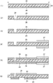
一般に、特性インピーダンスは、シングルエンドでは50Ω、差動線路では各信号配線において50Ωである。所望のインピーダンスを得るために高速信号を扱うプリント配線板では、図8に示すように、信号配線1とグランド配線2とがベース基材3を挟んで対向するように配置したマイクロストリップラインを適用している。
In general, the characteristic impedance is 50Ω at a single end, and 50Ω at each signal wiring in a differential line. In a printed wiring board that handles high-speed signals to obtain a desired impedance, a microstrip line is used in which
通常、マイクロストリップラインのグランド配線は、べたグランド、つまり信号配線の無い面全てがグランド層となっている構造を適用する。ただし、フレキシブルプリント配線板の場合、ベース基材の多くは25μmで、一般には12.5〜50μmと薄いために信号配線とグランド配線との間に発生するキャパシタンスが大きくなり、マイクロストリップラインの特性インピーダンスが下がってしまう。 Usually, the ground wiring of the microstrip line employs a structure in which a solid ground, that is, a surface having no signal wiring is a ground layer. However, in the case of a flexible printed wiring board, most of the base substrate is 25 μm, and generally 12.5 to 50 μm, so that the capacitance generated between the signal wiring and the ground wiring increases, and the characteristics of the microstrip line are large. Impedance drops.
例えば、厚さ100μmのガラス‐エポキシ系プリプレグ(比誘電率4)においてべたグランドのマイクロストリップラインを形成する場合、信号配線幅122μmで特性インピーダンス50Ωとなるが、25μmのポリイミド(比誘電率3.3)において同信号配線幅でマイクロストリップラインを形成した場合、特性インピーダンスは8Ω以下となってしまう。 For example, in the case where a solid ground microstrip line is formed in a glass-epoxy prepreg having a thickness of 100 μm (relative dielectric constant 4), a characteristic impedance of 50Ω is obtained with a signal wiring width of 122 μm. When the microstrip line is formed with the same signal wiring width in 3), the characteristic impedance becomes 8Ω or less.
同仕様にて信号配線−べたグランド間に発生するキャパシタンスを低減し、特性インピーダンスを50Ωとするためには、信号配線幅は17μmと狭くする必要がある。このような信号配線は導体を薄くすることで形成可能となるが、配線幅が狭く厚さも薄いため、直流抵抗が大きくなる。 In order to reduce the capacitance generated between the signal wiring and the solid ground with the same specification and to set the characteristic impedance to 50Ω, it is necessary to narrow the signal wiring width to 17 μm. Such a signal wiring can be formed by making the conductor thin, but since the wiring width is narrow and the thickness is thin, the DC resistance is increased.
また、信号配線幅が狭いため、形成する信号配線幅のぶれの影響を受け易く、所望のインピーダンスを精度良く得ることが困難となる。このため、グランド配線を正方形(特許文献1参照)、ないしはひし形(特許文献2参照)に刳り貫いたメッシュ形状が多く用いられている。 Further, since the signal wiring width is narrow, it is easily affected by fluctuations in the width of the signal wiring to be formed, and it becomes difficult to obtain a desired impedance with high accuracy. For this reason, a mesh shape is often used in which the ground wiring is formed in a square (see Patent Document 1) or a rhombus (see Patent Document 2).
しかし、メッシュグランド配線を適用した場合、信号配線がメッシュグランド配線の開口部に位置するか、グランド配線の導体部に位置するかにより特性インピーダンスが違うため不整合となり、信号の反射や損失の原因となる。 However, when mesh ground wiring is applied, mismatching occurs because the characteristic impedance differs depending on whether the signal wiring is located at the opening of the mesh ground wiring or at the conductor of the ground wiring, causing signal reflection and loss. It becomes.
また、信号配線が折れ曲がって配置されるような場合、折れ曲がる前における信号配線に対するメッシュ形状と折れ曲がった後の信号配線に対するメッシュ形状とが変わるため、特性インピーダンスが不整合となる。 Further, when the signal wiring is bent and arranged, the mesh shape with respect to the signal wiring before the bending and the mesh shape with respect to the signal wiring after the bending change, so that the characteristic impedance becomes inconsistent.
そこで、信号配線の曲線形状に対応してメッシュ形状を追従させる手法が提案されている(特許文献3参照)。あるいは曲線形状の外周と内周のメッシュ開口サイズをコントロールする、ないしは信号配線幅をコントロールする手法が提案されている(特許文献4参照)。
特許文献3に示したように曲線形状にメッシュを追従させる場合、曲線形状前後の信号配線に対するメッシュ形状は同じとなるが、曲線形状の信号配線に対するメッシュ形状は連続的に変化する。信号配線に対するメッシュ形状の変化がごく小さければその影響は無視できるが、その長さが伝送する周波数の1/4波長より長い場合、インピーダンスの不整合として影響が現れる。
When the mesh is made to follow a curved shape as shown in
一般に、反射防止の観点から曲線形状の信号配線は一定の曲率半径で曲がっており、曲率半径が大きいほど反射には有利である。例えば、曲率半径5mm、曲線形状角度90°の場合、曲線形状の長さは約7.9mmとなる。 In general, a curved signal wiring is bent with a certain radius of curvature from the viewpoint of preventing reflection, and the larger the radius of curvature, the more advantageous for reflection. For example, when the curvature radius is 5 mm and the curve shape angle is 90 °, the length of the curve shape is about 7.9 mm.
これは、フレキシブルプリント配線板に汎用されるポリイミド(εr=3.3)の、5GHzでの約1/4波長に相当する。この場合、5GHz以上の信号を伝送する際にインピーダンス不整合の影響が現れる。曲率半径がさらに大きくなれば曲線形状はさらに長くなり、結果として、インピーダンス不整合の影響が現れる周波数は低周波数にシフトする。 This corresponds to about ¼ wavelength at 5 GHz of polyimide (εr = 3.3) widely used for flexible printed wiring boards. In this case, the influence of impedance mismatching appears when transmitting a signal of 5 GHz or higher. As the radius of curvature increases further, the curve shape becomes longer, and as a result, the frequency at which the influence of impedance mismatching appears shifts to a lower frequency.
また、特許文献4に示されるように、曲線形状のメッシュ開口ないしは信号配線幅をコントロールする場合、製品ごとにメッシュ開口ないしは信号配線幅をシミュレートし、実際の製品にて検証し、必要に応じて再設計する、というサイクルが必要である。
Also, as shown in
このため、所望の特性を得るためには時間がかかり、大量生産には不向きである。また、メッシュに対し信号配線に露光や積層の位置合わせのずれが生じると、信号配線およびこれに対向するメッシュグランド配線の各面積が変わってしまい、所望のインピーダンスを得ることができなくなる。 For this reason, it takes time to obtain desired characteristics, and is not suitable for mass production. In addition, if the signal wiring is exposed or misaligned in the signal wiring with respect to the mesh, the areas of the signal wiring and the mesh ground wiring facing the signal wiring are changed, and a desired impedance cannot be obtained.
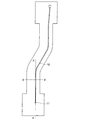
そこで、信号配線と線状のグランド配線とを平行に対向させることで、配線の曲線形状に拘わらず、信号配線に対するグランド配線の形状を一定にする方法が提案されている(特許文献5参照)。 Therefore, a method has been proposed in which the signal wiring and the linear ground wiring are opposed to each other in parallel, so that the shape of the ground wiring with respect to the signal wiring is made constant regardless of the curved shape of the wiring (see Patent Document 5). .
しかしながら、これら線状のグランド配線5の幅は、図9(a)に示すように必ず信号配線4の幅と同じであるか、あるいは太い。線状のグランド配線と信号配線との位置合わせずれがないと仮定した場合においても、これら線状のグランド配線は対向する信号配線と同じ面積であるため、信号配線−グランド配線間に発生するキャパシタンスは、べたグランドのそれと同じである。
However, the widths of these
したがって、信号配線−グランド配線間にフレキシブルプリント配線板のように薄い絶縁層を介する場合、前述のごとく大電流の伝送ができないか、あるいは精度良くインピーダンスを制御することが困難となる。 Therefore, when a thin insulating layer such as a flexible printed wiring board is interposed between the signal wiring and the ground wiring, it is difficult to transmit a large current as described above, or it is difficult to accurately control the impedance.
また、実際の製造工程においては、図9(b)に示すように位置合わせずれが発生し、信号配線6と対向するグランド配線7の面積が変わってしまい、所望のインピーダンスが得られなくなる。
Further, in the actual manufacturing process, as shown in FIG. 9B, misalignment occurs, the area of the
本発明は上述の点を考慮してなされたもので、べたグランドが適用できないフレキシブルプリント配線板のような薄い絶縁層を介するプリント配線板において、曲線形状がある場合においても信号配線に対するグランド配線の形状を一定とし、しかも露光ずれや積層ずれによって信号配線と対向するグランド配線の面積が変化しないマイクロストリップラインを提供することを目的とする。 The present invention has been made in consideration of the above points, and in a printed wiring board through a thin insulating layer such as a flexible printed wiring board to which a solid ground cannot be applied, even when there is a curved shape, the ground wiring for the signal wiring is not necessary. An object of the present invention is to provide a microstrip line that has a constant shape and does not change the area of the ground wiring that faces the signal wiring due to an exposure shift or a stacking shift.
本発明は、上記目的達成のため、
信号配線が曲線形状であるマイクロストリップライン構造を有するプリント配線板において、
絶縁層を介して前記信号配線に対向配置された線状のグランド配線をそなえ、
前記グランド配線の配線ピッチが前記信号配線の線幅の1/n(nは、1または2の自然数)である
ことを特徴とするプリント配線板、
を提供する。
In order to achieve the above object, the present invention
In the printed wiring board having a microstrip line structure in which the signal wiring has a curved shape,
A linear ground wiring disposed opposite to the signal wiring via an insulating layer;
A printed wiring board, wherein a wiring pitch of the ground wiring is 1 / n (n is a natural number of 1 or 2) of a line width of the signal wiring;
I will provide a.
(本発明の概要)
この構成により、図1にあるように、信号配線8に沿って線状のグランド配線9を対向して配置することで、信号配線の曲線形状によらず、信号配線に対するグランド配線の形状は常に一定となる。
(Outline of the present invention)
With this configuration, as shown in FIG. 1, by arranging linear ground wirings 9 along the
また、線状のグランド配線を信号配線幅に対し、1/nの配線ピッチとすることで、位置ずれが起きた際にも信号配線と対向するグランド配線の面積を一定に保つことが可能となる。ここで、nは1または2の自然数である。 In addition, by setting the linear ground wiring to a 1 / n wiring pitch with respect to the signal wiring width, it is possible to keep the area of the ground wiring facing the signal wiring constant even when misalignment occurs. Become. Here, n is a natural number of 1 or 2.
この際、ベース基材となる層間絶縁樹脂を、例えばポリイミド、液晶ポリマー、フッ素樹脂のような低誘電率の材料とすることで、信号配線とグランド配線との間に発生するキャパシタンスを低減できる。 At this time, the capacitance generated between the signal wiring and the ground wiring can be reduced by using a low dielectric constant material such as polyimide, liquid crystal polymer, or fluororesin for the interlayer insulating resin serving as the base substrate.
この結果、信号配線幅を太くすることができ、これと平行に配置される線状のグランド配線も太くすることができるため、エッチングによる加工の難度を低減することができる。 As a result, the signal wiring width can be increased, and the linear ground wiring arranged in parallel with the signal wiring width can be increased, so that the difficulty of processing by etching can be reduced.
また、これら材料は通常ガラスエポキシ基板に比べて誘電正接が低いため、高周波における誘電体損失を抑制することが可能となり、高速信号の伝送に有利である。 In addition, since these materials usually have a lower dielectric loss tangent than a glass epoxy substrate, dielectric loss at high frequencies can be suppressed, which is advantageous for high-speed signal transmission.
本発明によれば、フレキシブルプリント配線板のような薄い絶縁層を有するプリント配線板にマイクロストリップラインを形成する際、信号配線の曲線形状によらず信号配線に対するグランド配線形状が常に一定となり、また位置ずれがあっても信号配線に対向するグランド配線の面積を一定に保つことが可能となる。 According to the present invention, when a microstrip line is formed on a printed wiring board having a thin insulating layer such as a flexible printed wiring board, the ground wiring shape with respect to the signal wiring is always constant regardless of the curved shape of the signal wiring. Even if there is a misalignment, the area of the ground wiring facing the signal wiring can be kept constant.
これにより、高速信号の伝送に適したマイクロストリップライン構造を有するプリント配線板を提供することが可能となり、電子機器の小型化・高性能化に貢献することとなる。 As a result, a printed wiring board having a microstrip line structure suitable for high-speed signal transmission can be provided, which contributes to downsizing and high performance of electronic devices.
本発明の具体的実施例を挙げれば、ベース基材の厚さが12.5〜50μm、導体の厚さが5〜18μmの範囲にある材料を用いて、信号配線の幅を25〜500μmの範囲とし、線状のグランド配線の配線ピッチを25〜500μmの範囲とすることで、特性インピーダンス50Ωのマイクロストリップラインを形成することが可能となる。 In a specific example of the present invention, the width of the signal wiring is 25 to 500 μm using a material having a base substrate thickness of 12.5 to 50 μm and a conductor thickness of 5 to 18 μm. By setting the range and the wiring pitch of the linear ground wiring in the range of 25 to 500 μm, a microstrip line having a characteristic impedance of 50Ω can be formed.
また、これらマイクロストリップラインは、高精度に形状を制御する必要がある。層間接続のためのめっきを行った後にマイクロストリップラインを形成しようとすると、めっきの厚さのばらつきにより、形状にばらつきが生じ、インピーダンスを精度良くコントロールすることが困難となる。 Moreover, it is necessary to control the shape of these microstrip lines with high accuracy. If an attempt is made to form a microstrip line after performing plating for interlayer connection, variations in the thickness occur due to variations in the thickness of the plating, making it difficult to accurately control the impedance.
このため、層間導通のためのめっきを行う前に予め信号配線および線状のグランド配線を形成し、当該箇所を除去可能な保護膜でマスキングし、層間導通のためのめっきを行い、保護膜を除去することで信号配線および線状のグランド配線の形状を精度よく形成することが可能となり、延いてはインピーダンスコントロールの精度が向上する。 For this reason, before performing plating for interlayer conduction, signal wiring and linear ground wiring are formed in advance, masked with a protective film that can be removed, and plating for interlayer conduction is performed. By removing, it becomes possible to form the signal wiring and the linear ground wiring with high accuracy, thereby improving the accuracy of impedance control.
以下、添付図面を参照して本発明の実施例を説明する。 Embodiments of the present invention will be described below with reference to the accompanying drawings.
図2は、本発明の一実施例によるマイクロストリップラインの断面図である。 FIG. 2 is a cross-sectional view of a microstrip line according to an embodiment of the present invention.
出発材料は、ここでは両面銅張り積層板として、メタロイヤル(東洋メタライジング株式会社製)PI−25D−CCW−08D0(#25)を用いた。 The starting material used here was Meta Royal (Toyo Metallizing Co., Ltd.) PI-25D-CCW-08D0 (# 25) as a double-sided copper-clad laminate.
当該材料を選定した理由は、2点ある。 There are two reasons for selecting the material.
(1)マイクロストリップラインにおいて、ベース基材の誘電率が高いと、グランド配線との間に発生するキャパシタンスが大きくなるため、所望の特性インピーダンスを得るためには信号配線の幅を狭くしなければならない。 (1) In the microstrip line, if the dielectric constant of the base substrate is high, the capacitance generated between the base wiring and the ground wiring increases. Therefore, in order to obtain a desired characteristic impedance, the width of the signal wiring must be reduced. Don't be.
しかし、信号配線幅を狭くすると配線形成の難易度が高くなり、精度の良いインピーダンスコントロールができなくなる。したがって、ベース基材は誘電率の低いポリイミドが望ましい。 However, if the signal wiring width is narrowed, the difficulty of wiring formation increases, and accurate impedance control cannot be performed. Accordingly, the base substrate is preferably a polyimide having a low dielectric constant.
(2)銅張り板の銅箔は、通常ベース基材との接着力を確保するために、裏面処理と呼ばれる粗化処理が施されている。しかし、裏面処理によるインダクタンスの増大が特性インピーダンスの制御に不利である。したがって、裏面処理のない銅張り板が望ましい。 (2) The copper foil of the copper-clad plate is usually subjected to a roughening treatment called back surface treatment in order to ensure adhesion with the base substrate. However, an increase in inductance due to the backside treatment is disadvantageous for controlling characteristic impedance. Therefore, a copper-clad plate without backside treatment is desirable.
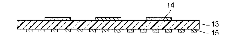
ここで、ベース基材であるポリイミド10の厚さは25μm、銅箔の厚さは8μmである。本材料を用いてマイクロストリップラインを形成する。そして、マイクロストリップラインのグランド配線12は信号配線11に沿った線状とし、その配線ピッチは信号配線幅の1/nとする(ここで、nは1または2の自然数とする)。
Here, the thickness of the
特性インピーダンス50Ωを実現するため、ここでは、一例として信号配線幅を92μm、n=1、グランド配線の配線ピッチを92μm、グランド配線幅を46μmとし、グランド配線の配線本数は信号配線本数3に対し7本とした。 In order to realize the characteristic impedance of 50Ω, here, as an example, the signal wiring width is 92 μm, n = 1, the ground wiring pitch is 92 μm, the ground wiring width is 46 μm, and the number of ground wirings is 3 Seven.
図3は、本発明の実施例2の断面図である。この実施例2では、ベース基材13を、実施例1におけるポリイミドに代えて、より誘電率の低い液晶ポリマーとした。これにより、信号配線とグランド配線との間に発生するキャパシタンスがより低減されるため、信号配線幅の加工難易度を抑制することが可能となる。
FIG. 3 is a cross-sectional view of
また、液晶ポリマーは、ポリイミドに比べて誘電正接が低いため高周波領域における誘電体損失を抑制でき、高速信号の伝送に有利である。出発材料は、ここでは両面銅張り積層板エスパネックスLB−09−25−09NE(新日鐵化学株式会社製)を用いた。 In addition, since the liquid crystal polymer has a lower dielectric loss tangent than polyimide, the dielectric loss in the high frequency region can be suppressed, which is advantageous for high-speed signal transmission. Here, double-sided copper-clad laminate Espanex LB-09-25-09NE (manufactured by Nippon Steel Chemical Co., Ltd.) was used as the starting material.
この場合、ベース基材である液晶ポリマーの厚さは25μmであり、銅箔の厚さは元の厚さ9μmをハーフエッチングにより5μmとした。このハーフエッチングを行った材料を用いて、マイクロストリップラインを形成する。 In this case, the thickness of the liquid crystal polymer as the base substrate was 25 μm, and the thickness of the copper foil was 5 μm by half etching the original thickness of 9 μm. Using the half-etched material, a microstrip line is formed.
マイクロストリップラインのグランド配線15は、信号配線14に沿った線状とし、その配線ピッチは信号配線幅の1/nとする(ここで、nは1または2の自然数とする)。
The
特性インピーダンス50Ωを実現するため、ここでは一例として信号配線幅を100μm、n=2、グランド配線の配線ピッチを50μm、グランド配線幅を25μmとし、グランド配線の配線本数は信号配線の本数3本に対し14本とした。 In order to realize a characteristic impedance of 50Ω, here, as an example, the signal wiring width is 100 μm, n = 2, the ground wiring pitch is 50 μm, the ground wiring width is 25 μm, and the number of ground wirings is three. In contrast, 14 were used.
図4は本発明の実施例3の平面図を示し、図5Aおよび図5Bはそれぞれ図4におけるA−A’線およびB−B’線に沿う断面図を示す。
4 is a plan view of
まず、図5A(1)に示すように、銅箔の厚さが4μmの両面銅張り積層板16を用意する。この材料としては、実施例1で示した理由により、例えば両面銅張り積層板「メタロイヤル(東洋メタライジング株式会社製)PI−25D−CCW−04D0(#25)」などが挙げられる。
First, as shown in FIG. 5A (1), a double-sided copper-clad
次いで図5A(2)に示すように、層間接続用のビアとなる穴17を形成する。ビアの種類は、貫通、非貫通を問わない。また、穴の形成方法としては、貫通であれば機械的なドリル、パンチ、レーザードリル、プラズマ、化学エッチングなどが挙げられ、非貫通であればレーザードリル、プラズマ、化学エッチングなどが挙げられる。ここでは、UV−YAGレーザにて直径50μmの貫通穴を形成した。
Next, as shown in FIG. 5A (2), a
さらに図5B(3)に示すように、マイクロストリップラインを形成する。マイクロストリップラインのグランド配線19は、信号配線18に沿った線状とし、その配線ピッチは信号配線幅の1/nとする(ここで、nは1または2の自然数とする)。
Further, as shown in FIG. 5B (3), a microstrip line is formed. The
ここでは一例として、信号配線の幅を96μm、n=2、グランド配線の配線ピッチを48μm、グランド配線の幅を24μmとし、特性インピーダンスを50Ωとした。また、グランド配線の配線本数は、信号配線の本数5に対し11本とした。 Here, as an example, the width of the signal wiring is 96 μm, n = 2, the wiring pitch of the ground wiring is 48 μm, the width of the ground wiring is 24 μm, and the characteristic impedance is 50Ω. In addition, the number of ground wirings was 11 with respect to 5 signal wirings.
この後、図5A(4)に示すように、図5B(3)で形成したグランド配線および信号配線に保護層20を形成した。保護層20の素材は、この後に行う層間接続のためのめっき工程に耐え、その後、剥離可能なものであれば特に限定されるものではない。ここでは、厚さ20μmのドライフィルムレジストSPG202(旭化成エレクトロニクス株式会社製)をラミネートし、グランド配線および信号配線にのみ露光し、現像した。
Thereafter, as shown in FIG. 5A (4), a
次いで、図5A(5)に示すように、層間接続のためのめっき21を行う。信号配線およびグランド配線は保護層により被覆されているため、めっきが析出することはない。ただし、めっきの厚さは保護層の厚さより薄くし、ここでは10μmとした。 Next, as shown in FIG. 5A (5), plating 21 for interlayer connection is performed. Since the signal wiring and the ground wiring are covered with a protective layer, plating does not deposit. However, the thickness of the plating was made thinner than the thickness of the protective layer, and here it was 10 μm.
最後に、図5A(6)に示すように、保護膜を剥離、マイクロストリップラインを除く箇所の配線パターン22を形成する。この際、ビア17のランド径は、先に形成した信号配線18およびグランド配線19と、後から形成する配線パターン22との露光位置ずれを考慮した径とする。
Finally, as shown in FIG. 5A (6), the protective film is peeled off, and the
以上により、高精度でインピーダンスが制御されたマイクロストリップラインを有するフレキシブルプリント配線板を形成することが可能である。 As described above, it is possible to form a flexible printed wiring board having a microstrip line whose impedance is controlled with high accuracy.
図6は本発明の実施例4の平面図を示し、図7Aおよび図7Bはそれぞれ図6におけるA−A’線およびB−B’線に沿う断面図を示す。
6 is a plan view of
まず、図7A(1)に示すように、銅箔の厚さが9μmの両面銅張り積層板23を用意する。ここでは、実施例1および同2で示した理由により、両面銅張り積層板エスパネックスLB−09−25−09NE(新日鐵化学株式会社製、銅箔の厚さ9μm)を適用した。
First, as shown in FIG. 7A (1), a double-sided copper-clad
次いで、図7A(2)に示すように層間接続用のビアとなる穴24を形成する。ビアの種類は、貫通、非貫通を問わない。また、穴の形成方法としては、貫通であれば機械的なドリル、パンチ、レーザードリル、プラズマ、化学エッチングなどが挙げられ、非貫通であればレーザードリル、プラズマ、化学エッチングなどが挙げられ、特に限定するものではない。ここでは、UV−YAGレーザにて直径50μmの非貫通穴を形成した。
Next, as shown in FIG. 7A (2), a
さらに、図7B(3)に示すごとく、マイクロストリップラインを形成する。ここで、マイクロストリップラインのグランド配線26は信号配線25に沿った線状とし、その配線ピッチは信号配線幅の1/nとする(ここで、nは1または2の自然数とする)。
Further, as shown in FIG. 7B (3), a microstrip line is formed. Here, the
ここでは一例として、信号配線幅を100μm、n=1、グランド配線の配線ピッチを100μm、グランド配線幅を50μmとし、特性インピーダンスを50Ωとした。また、グランド配線の配線本数は、信号配線の本数5に対し11本とした。 Here, as an example, the signal wiring width is 100 μm, n = 1, the wiring pitch of the ground wiring is 100 μm, the ground wiring width is 50 μm, and the characteristic impedance is 50Ω. In addition, the number of ground wirings was 11 with respect to 5 signal wirings.
この後、図7A(4)に示すように、図7A(3)で形成したグランド配線および信号配線に保護層27を形成した。保護層27の素材は、この後に行う層間接続のためのめっき工程に耐え、その後、剥離可能なものであれば特に限定されるものではない。
Thereafter, as shown in FIG. 7A (4), a
ここでは、厚さ20μmのドライフィルムレジストSPG202(旭化成エレクトロニクス株式会社製)をラミネートし、グランド配線および信号配線にのみ露光し、現像した。 Here, a dry film resist SPG202 (manufactured by Asahi Kasei Electronics Co., Ltd.) having a thickness of 20 μm was laminated, and only the ground wiring and the signal wiring were exposed and developed.
次いで、図7A(5)に示すように、層間接続のためのめっき28を行う。信号配線、およびグランド配線は保護層により被覆されているため、めっきが析出することはない。ただし、めっき厚さは保護層の厚さより薄くし、ここでは10μmとした。 Next, as shown in FIG. 7A (5), plating 28 for interlayer connection is performed. Since the signal wiring and the ground wiring are covered with the protective layer, plating does not deposit. However, the plating thickness was made thinner than the thickness of the protective layer, and here it was 10 μm.
最後に、図7A(6)に示すように、保護膜を剥離、マイクロストリップラインを除く箇所の配線パターン29を形成する。この際、ビア24のランド径は、先に形成した信号配線125およびグランド配線26と、後から形成する配線パターン29との露光位置ずれを考慮した径とする。
Finally, as shown in FIG. 7A (6), the protective film is peeled off, and a
以上により、高精度でインピーダンスが制御されたマイクロストリップラインを有するフレキシブルプリント配線板を形成することが可能である。 As described above, it is possible to form a flexible printed wiring board having a microstrip line whose impedance is controlled with high accuracy.
1 信号配線
2 べたグランド
3 ベース基材
4 信号配線
5 線状のグランド配線
6 信号配線
7 位置ずれした線状のグランド配線
8 信号配線
9 線状のグランド配線
10 ポリイミド
11 信号配線
12 線状のグランド配線
13 液晶ポリマー
14 信号配線
15 線状のグランド配線
16 両面銅張り積層板
17 穴
18 信号配線
19 線状のグランド配線
20 保護層
21 めっき
22 信号配線、グランド配線を除く配線パターン
23 両面銅張り積層板
24 穴
25 信号配線
26 線状のグランド配線
27 保護層
28 めっき
29 信号配線、グランド配線を除く配線パターン
DESCRIPTION OF
Claims (1)
前記絶縁層を介して前記信号配線に対向配置された線状のグランド配線をそなえ、
前記グランド配線の配線ピッチが前記信号配線の線幅の1/n(nは、1または2の自然数)である
ことを特徴とするプリント配線板。 In a printed wiring board having a microstrip line structure in which the signal wiring arranged on the insulating layer has a curved shape,
A linear ground wiring disposed opposite to the signal wiring via the insulating layer;
The printed wiring board, wherein a wiring pitch of the ground wiring is 1 / n (n is a natural number of 1 or 2) of a line width of the signal wiring.
Priority Applications (8)
| Application Number | Priority Date | Filing Date | Title |
|---|---|---|---|
| JP2007150036A JP4912960B2 (en) | 2007-06-06 | 2007-06-06 | Printed wiring board |
| EP08704242A EP2031944B1 (en) | 2007-06-06 | 2008-01-31 | Printed wiring board |
| KR1020087018224A KR20100017038A (en) | 2007-06-06 | 2008-01-31 | Printed wiring board |
| PCT/JP2008/051491 WO2008149572A1 (en) | 2007-06-06 | 2008-01-31 | Printed wiring board |
| AT08704242T ATE531239T1 (en) | 2007-06-06 | 2008-01-31 | CIRCUIT BOARD |
| US12/223,467 US8040198B2 (en) | 2007-06-06 | 2008-01-31 | Printed wiring board having wire grounding conductors with distances that are 1/n the width of the signal lines |
| CN2008800000625A CN101543142B (en) | 2007-06-06 | 2008-01-31 | printed wiring board |
| TW097106621A TWI403226B (en) | 2007-06-06 | 2008-02-26 | Printed wiring board |
Applications Claiming Priority (1)
| Application Number | Priority Date | Filing Date | Title |
|---|---|---|---|
| JP2007150036A JP4912960B2 (en) | 2007-06-06 | 2007-06-06 | Printed wiring board |
Publications (2)
| Publication Number | Publication Date |
|---|---|
| JP2008305884A JP2008305884A (en) | 2008-12-18 |
| JP4912960B2 true JP4912960B2 (en) | 2012-04-11 |
Family
ID=40093401
Family Applications (1)
| Application Number | Title | Priority Date | Filing Date |
|---|---|---|---|
| JP2007150036A Active JP4912960B2 (en) | 2007-06-06 | 2007-06-06 | Printed wiring board |
Country Status (8)
| Country | Link |
|---|---|
| US (1) | US8040198B2 (en) |
| EP (1) | EP2031944B1 (en) |
| JP (1) | JP4912960B2 (en) |
| KR (1) | KR20100017038A (en) |
| CN (1) | CN101543142B (en) |
| AT (1) | ATE531239T1 (en) |
| TW (1) | TWI403226B (en) |
| WO (1) | WO2008149572A1 (en) |
Families Citing this family (8)
| Publication number | Priority date | Publication date | Assignee | Title |
|---|---|---|---|---|
| JP5436361B2 (en) * | 2010-07-30 | 2014-03-05 | 日東電工株式会社 | Wiring circuit board and manufacturing method thereof |
| CN101925252A (en) * | 2010-08-05 | 2010-12-22 | 浪潮电子信息产业股份有限公司 | A Wiring Method for Improving Signal Quality |
| US20150016069A1 (en) * | 2013-07-09 | 2015-01-15 | Shenzhen China Star Optoelectronics Technology Co., Ltd. | Printed circuit board |
| CN103338586A (en) * | 2013-07-09 | 2013-10-02 | 深圳市华星光电技术有限公司 | Printed circuit board |
| US10136512B2 (en) * | 2014-12-09 | 2018-11-20 | Microsoft Technology Licensing, Llc | Avoiding reflections in PCB signal trace |
| US9747934B1 (en) * | 2016-09-13 | 2017-08-29 | Seagate Technology Llc | Flexible dynamic loop with back-side impedance control structures |
| CN110798977B (en) * | 2018-08-01 | 2021-03-23 | 鹏鼎控股(深圳)股份有限公司 | Thin antenna circuit board and manufacturing method thereof |
| JP2021145061A (en) * | 2020-03-12 | 2021-09-24 | 京セラ株式会社 | Flexible wiring board |
Family Cites Families (19)
| Publication number | Priority date | Publication date | Assignee | Title |
|---|---|---|---|---|
| US4680557A (en) * | 1985-04-22 | 1987-07-14 | Tektronix, Inc. | Staggered ground-plane microstrip transmission line |
| JPS629697A (en) * | 1985-07-08 | 1987-01-17 | 株式会社日立製作所 | wiring board |
| CA2154156C (en) * | 1993-02-02 | 2005-04-26 | Edward D. Suski | A circuit board arrangement including shielding grids, and constructing thereof |
| JPH07235741A (en) * | 1993-12-27 | 1995-09-05 | Ngk Spark Plug Co Ltd | Multilayer wiring board |
| US5764489A (en) * | 1996-07-18 | 1998-06-09 | Compaq Computer Corporation | Apparatus for controlling the impedance of high speed signals on a printed circuit board |
| JPH10145112A (en) * | 1996-11-14 | 1998-05-29 | Toshiba Corp | Wiring board |
| US5818315A (en) * | 1996-12-31 | 1998-10-06 | Lucent Technologies Inc. | Signal trace impedance control using a grid-like ground plane |
| TW476229B (en) | 1998-08-24 | 2002-02-11 | Adv Flexible Circuits Co Ltd | Circuit board having shielding plate with empty-hole opening pattern to control impedance and transmission time |
| JP3307597B2 (en) | 1998-09-30 | 2002-07-24 | 株式会社 アドテック | Printed wiring device |
| JP2001085805A (en) * | 1999-09-17 | 2001-03-30 | Kyoden:Kk | Printed board |
| JP4680410B2 (en) * | 2001-04-24 | 2011-05-11 | 日本特殊陶業株式会社 | Wiring board |
| JP4063533B2 (en) * | 2001-12-10 | 2008-03-19 | 日本碍子株式会社 | Flexible wiring board |
| US6885549B2 (en) * | 2002-04-11 | 2005-04-26 | Dell Products L.P. | System and method for flexible circuits |
| JP2004140308A (en) * | 2002-10-16 | 2004-05-13 | Adorinkusu:Kk | Printed wiring board for high-speed signal using slit method |
| JP4148069B2 (en) * | 2003-08-28 | 2008-09-10 | ソニー株式会社 | Substrate having microstrip line structure, semiconductor device having microstrip line structure, and method of manufacturing substrate having microstrip line structure |
| JP2005317631A (en) * | 2004-04-27 | 2005-11-10 | Alps Electric Co Ltd | Electronic circuit board |
| JP2006147837A (en) | 2004-11-19 | 2006-06-08 | Sony Chem Corp | Wiring substrate, method of arrangement of wiring pattern |
| JP2006173310A (en) | 2004-12-15 | 2006-06-29 | Sumitomo Bakelite Co Ltd | Circuit board |
| JP2007141990A (en) * | 2005-11-16 | 2007-06-07 | Sumitomo Bakelite Co Ltd | Circuit board |
-
2007
- 2007-06-06 JP JP2007150036A patent/JP4912960B2/en active Active
-
2008
- 2008-01-31 CN CN2008800000625A patent/CN101543142B/en not_active Expired - Fee Related
- 2008-01-31 US US12/223,467 patent/US8040198B2/en not_active Expired - Fee Related
- 2008-01-31 KR KR1020087018224A patent/KR20100017038A/en not_active Withdrawn
- 2008-01-31 EP EP08704242A patent/EP2031944B1/en not_active Not-in-force
- 2008-01-31 AT AT08704242T patent/ATE531239T1/en not_active IP Right Cessation
- 2008-01-31 WO PCT/JP2008/051491 patent/WO2008149572A1/en not_active Ceased
- 2008-02-26 TW TW097106621A patent/TWI403226B/en active
Also Published As
| Publication number | Publication date |
|---|---|
| ATE531239T1 (en) | 2011-11-15 |
| EP2031944B1 (en) | 2011-10-26 |
| US8040198B2 (en) | 2011-10-18 |
| KR20100017038A (en) | 2010-02-16 |
| CN101543142A (en) | 2009-09-23 |
| TW200850086A (en) | 2008-12-16 |
| CN101543142B (en) | 2011-07-06 |
| EP2031944A4 (en) | 2009-12-09 |
| EP2031944A1 (en) | 2009-03-04 |
| TWI403226B (en) | 2013-07-21 |
| WO2008149572A1 (en) | 2008-12-11 |
| JP2008305884A (en) | 2008-12-18 |
| US20100231331A1 (en) | 2010-09-16 |
Similar Documents
| Publication | Publication Date | Title |
|---|---|---|
| JP4912960B2 (en) | Printed wiring board | |
| US11089674B2 (en) | Wiring substrate and method for manufacturing wiring substrate | |
| US7897055B2 (en) | Method for manufacturing multilayer flexible printed circuit board | |
| US7581312B2 (en) | Method for manufacturing multilayer flexible printed circuit board | |
| JP6732723B2 (en) | Printed wiring board for high frequency transmission | |
| US11696391B2 (en) | Wiring substrate and method of manufacturing the same | |
| US20190387613A1 (en) | Printed wiring board and method for manufacturing same | |
| US20040150487A1 (en) | Semi-suspended coplanar waveguide on a printed circuit board | |
| JP2006173239A (en) | WIRING BOARD, MANUFACTURING METHOD THEREOF, AND ELECTRONIC DEVICE USING THE SAME | |
| US11700685B2 (en) | Method for manufacturing the same | |
| JPH07106766A (en) | Flex-rigid multilayer board and manufacturing method thereof | |
| JP4363947B2 (en) | Multilayer wiring circuit board and method for manufacturing the same | |
| JP5617374B2 (en) | Printed wiring board | |
| WO2021102740A1 (en) | High-frequency transmission circuit board and manufacturing method therefor | |
| JP7644796B2 (en) | Flexible Printed Wiring Boards | |
| CN115426765B (en) | High-frequency board and method for manufacturing high-frequency board | |
| JP2006080162A (en) | Printed wiring board | |
| KR102166048B1 (en) | Multilayer circuit board | |
| JP2009088337A (en) | Printed circuit board and its manufacturing method | |
| CN121240315A (en) | Flexible circuit boards and their manufacturing methods | |
| KR100588770B1 (en) | Double-sided flexible circuit board and manufacturing method | |
| JP2008311270A (en) | Printed wiring board and its manufacturing method | |
| JP6875942B2 (en) | Manufacturing method of printed wiring board | |
| CN113966085A (en) | Circuit board and manufacturing method thereof | |
| CN114762460A (en) | Circuit board and manufacturing method thereof |
Legal Events
| Date | Code | Title | Description |
|---|---|---|---|
| A621 | Written request for application examination |
Free format text: JAPANESE INTERMEDIATE CODE: A621 Effective date: 20100105 |
|
| TRDD | Decision of grant or rejection written | ||
| A01 | Written decision to grant a patent or to grant a registration (utility model) |
Free format text: JAPANESE INTERMEDIATE CODE: A01 Effective date: 20111222 |
|
| A01 | Written decision to grant a patent or to grant a registration (utility model) |
Free format text: JAPANESE INTERMEDIATE CODE: A01 |
|
| A61 | First payment of annual fees (during grant procedure) |
Free format text: JAPANESE INTERMEDIATE CODE: A61 Effective date: 20120118 |
|
| R150 | Certificate of patent or registration of utility model |
Ref document number: 4912960 Country of ref document: JP Free format text: JAPANESE INTERMEDIATE CODE: R150 Free format text: JAPANESE INTERMEDIATE CODE: R150 |
|
| FPAY | Renewal fee payment (event date is renewal date of database) |
Free format text: PAYMENT UNTIL: 20150127 Year of fee payment: 3 |
|
| R250 | Receipt of annual fees |
Free format text: JAPANESE INTERMEDIATE CODE: R250 |
|
| R250 | Receipt of annual fees |
Free format text: JAPANESE INTERMEDIATE CODE: R250 |
|
| R250 | Receipt of annual fees |
Free format text: JAPANESE INTERMEDIATE CODE: R250 |
|
| R250 | Receipt of annual fees |
Free format text: JAPANESE INTERMEDIATE CODE: R250 |
|
| R250 | Receipt of annual fees |
Free format text: JAPANESE INTERMEDIATE CODE: R250 |
|
| R250 | Receipt of annual fees |
Free format text: JAPANESE INTERMEDIATE CODE: R250 |
|
| R250 | Receipt of annual fees |
Free format text: JAPANESE INTERMEDIATE CODE: R250 |
|
| R250 | Receipt of annual fees |
Free format text: JAPANESE INTERMEDIATE CODE: R250 |
|
| R250 | Receipt of annual fees |
Free format text: JAPANESE INTERMEDIATE CODE: R250 |
|
| R250 | Receipt of annual fees |
Free format text: JAPANESE INTERMEDIATE CODE: R250 |
|
| R250 | Receipt of annual fees |
Free format text: JAPANESE INTERMEDIATE CODE: R250 |
|
| S533 | Written request for registration of change of name |
Free format text: JAPANESE INTERMEDIATE CODE: R313533 |
|
| R350 | Written notification of registration of transfer |
Free format text: JAPANESE INTERMEDIATE CODE: R350 |