JP4862906B2 - Clock distribution apparatus and clock distribution method - Google Patents
Clock distribution apparatus and clock distribution method Download PDFInfo
- Publication number
- JP4862906B2 JP4862906B2 JP2009069411A JP2009069411A JP4862906B2 JP 4862906 B2 JP4862906 B2 JP 4862906B2 JP 2009069411 A JP2009069411 A JP 2009069411A JP 2009069411 A JP2009069411 A JP 2009069411A JP 4862906 B2 JP4862906 B2 JP 4862906B2
- Authority
- JP
- Japan
- Prior art keywords
- clock
- phase
- phase difference
- circuit
- delay
- Prior art date
- Legal status (The legal status is an assumption and is not a legal conclusion. Google has not performed a legal analysis and makes no representation as to the accuracy of the status listed.)
- Expired - Fee Related
Links
Images


Classifications
-
- H—ELECTRICITY
- H03—ELECTRONIC CIRCUITRY
- H03L—AUTOMATIC CONTROL, STARTING, SYNCHRONISATION, OR STABILISATION OF GENERATORS OF ELECTRONIC OSCILLATIONS OR PULSES
- H03L7/00—Automatic control of frequency or phase; Synchronisation
- H03L7/06—Automatic control of frequency or phase; Synchronisation using a reference signal applied to a frequency- or phase-locked loop
- H03L7/08—Details of the phase-locked loop
- H03L7/081—Details of the phase-locked loop provided with an additional controlled phase shifter
-
- G—PHYSICS
- G06—COMPUTING; CALCULATING OR COUNTING
- G06F—ELECTRIC DIGITAL DATA PROCESSING
- G06F1/00—Details not covered by groups G06F3/00 - G06F13/00 and G06F21/00
- G06F1/04—Generating or distributing clock signals or signals derived directly therefrom
- G06F1/10—Distribution of clock signals, e.g. skew
-
- H—ELECTRICITY
- H03—ELECTRONIC CIRCUITRY
- H03L—AUTOMATIC CONTROL, STARTING, SYNCHRONISATION, OR STABILISATION OF GENERATORS OF ELECTRONIC OSCILLATIONS OR PULSES
- H03L7/00—Automatic control of frequency or phase; Synchronisation
- H03L7/06—Automatic control of frequency or phase; Synchronisation using a reference signal applied to a frequency- or phase-locked loop
- H03L7/07—Automatic control of frequency or phase; Synchronisation using a reference signal applied to a frequency- or phase-locked loop using several loops, e.g. for redundant clock signal generation
-
- H—ELECTRICITY
- H03—ELECTRONIC CIRCUITRY
- H03L—AUTOMATIC CONTROL, STARTING, SYNCHRONISATION, OR STABILISATION OF GENERATORS OF ELECTRONIC OSCILLATIONS OR PULSES
- H03L7/00—Automatic control of frequency or phase; Synchronisation
- H03L7/06—Automatic control of frequency or phase; Synchronisation using a reference signal applied to a frequency- or phase-locked loop
- H03L7/08—Details of the phase-locked loop
- H03L7/085—Details of the phase-locked loop concerning mainly the frequency- or phase-detection arrangement including the filtering or amplification of its output signal
- H03L7/091—Details of the phase-locked loop concerning mainly the frequency- or phase-detection arrangement including the filtering or amplification of its output signal the phase or frequency detector using a sampling device
Description
本発明は、クロック分配装置及びクロック分配方法に関し、特に異なる系統のクロック間のクロック・スキューの低減が可能なクロック分配装置及びクロック分配方法に関する。 The present invention relates to a clock distribution device and a clock distribution method, and more particularly to a clock distribution device and a clock distribution method capable of reducing clock skew between clocks of different systems.
論理回路では、クロックを用いた同期動作を行うことが多い。クロックは論理回路内の各所に分配されるので、分配されたクロック間に、クロックの位相差、いわゆる「クロック・スキュー」が発生することがある。クロックを用いた同期回路では、クロック・スキューは極力小さいことが望ましい。そして、クロックが高速になるほど、クロック・スキューが論路回路の動作に与える影響は大きい。そのため、高速なクロックで動作する回路ほど、クロック・スキューを低減させる必要がある。 Logic circuits often perform a synchronous operation using a clock. Since the clock is distributed to various locations in the logic circuit, a clock phase difference, so-called “clock skew”, may occur between the distributed clocks. In a synchronous circuit using a clock, it is desirable that the clock skew is as small as possible. The higher the clock speed, the greater the influence of clock skew on the logical circuit operation. Therefore, it is necessary to reduce the clock skew as the circuit operates with a high-speed clock.
一方、回路の物理的な規模が大きくなるほど、クロック・スキューが大きくなるという問題がある。例えば、半導体集積回路では、チップ・サイズが大きくなるにつれて、クロックの供給源からクロックの供給先までのクロック・ラインの、最も長いものの配線長と最も短いものの配線長との差が大きくなる。そのため、クロックの供給源からクロック供給先までの伝達遅延時間のバラツキが大きくなり、クロック・スキューが大きくなる。 On the other hand, there is a problem that the clock skew increases as the physical scale of the circuit increases. For example, in a semiconductor integrated circuit, as the chip size increases, the difference between the longest wiring length and the shortest wiring length of the clock line from the clock supply source to the clock supply destination increases. For this reason, the variation in the transmission delay time from the clock supply source to the clock supply destination increases, and the clock skew increases.
ところで、高速なクロックを用いる回路では、低速なクロックを高速なクロックに逓倍するためにPLL(Phase Locked Loop)を用いることがある。高速なクロックは回路内部の各所に分配され、データの同期転送等に用いられる。PLLを用いる場合におけるクロック・スキューの低減策として、1つのPLLから分配されるクロックが分配される回路の領域を狭くする方法がある。この方法では、回路内に複数のPLLを備えることが前提となる。この方法を用いる場合においても、異なるPLLから分配されたクロックを用いる回路間に同期関係が必要なパスが存在する場合がある。その場合も、クロック間のスキューが大きければ正常な同期動作ができないという課題がある。 By the way, in a circuit using a high-speed clock, a PLL (Phase Locked Loop) may be used to multiply a low-speed clock to a high-speed clock. A high-speed clock is distributed to various places in the circuit and used for synchronous transfer of data. As a measure for reducing clock skew in the case of using a PLL, there is a method of narrowing an area of a circuit to which a clock distributed from one PLL is distributed. This method assumes that a plurality of PLLs are provided in the circuit. Even when this method is used, there may be a path that requires a synchronous relationship between circuits that use clocks distributed from different PLLs. Even in this case, there is a problem that normal synchronization operation cannot be performed if the skew between clocks is large.
複数のPLLを用いる場合における、クロック・スキュー低減のための技術がある(例えば、特許文献1、特許文献2参照。)。特許文献1のクロック分配回路では、複数のPLLがそれぞれクロック・ツリーを構成する。「クロック・ツリー」とは、クロック・ラインが、分岐を繰り返すことによって、全体として樹枝状(ツリー状)の配線を構成したものをいう。それぞれのクロック・ツリーの所定の分岐点からのクロックは、各々のPLLにフィードバックされ、PLLに入力される基準クロックと位相を合わせられる。基準クロックは、全PLLに共通に入力されている。従って、各々のクロック・ツリーの分岐点からのクロック同士の位相を合わせることができる。すなわち、クロック・ツリー間のクロック・スキューが低減される。
There are techniques for reducing clock skew in the case of using a plurality of PLLs (see, for example,
特許文献2記載のクロック供給装置では、2系統のクロックの各々が、互いに相手側との位相を合わせるように、可変遅延回路を制御する。従って、2系統のクロック間のクロック・スキューが低減される。 In the clock supply device described in Patent Document 2, the variable delay circuit is controlled so that each of the two systems of clocks is in phase with the counterpart. Therefore, the clock skew between the two clocks is reduced.
特許文献1に記載されたクロック分配回路では、図11に示すように、PLLに供給される基準クロックの位相とクロック・ツリーの所定の分岐点から分配されるクロックとの位相を、PLLを用いて合わせている。ところが、基準クロックを各々のPLLに入力するための配線においても、クロックの伝達遅延がある。そのため、各々のPLLに入力される基準クロック自体にクロック・スキューが生じる。従って、個々のクロック・ツリーにおけるクロックの位相を各々のPLLの基準クロックの位相に合わせても、クロック・ツリー間のクロック・スキューは十分に低減できないという課題がある。
In the clock distribution circuit described in
また、基準クロックと位相が比較されるクロックとしてPLLに入力されるクロックは、クロック・ツリーの所定の分岐点からフィードバックされる。ところが、PLLからクロックの分岐点までのクロック・ライン、及びクロックのフィードバックのための配線には、伝達遅延時間が存在する。そして、その伝達遅延時間は、半導体プロセス等、製造バラツキのために一定値にはならない。また、クロックには、回路が動作することによって発生するノイズや立ち上がり時間、立ち下がり時間のバラツキ等によってクロック・ジッターが発生する。そのため、個々のPLLにフィードバックされるクロック間にも大きなクロック・スキューが存在し、従って、PLLの出力にもクロック・スキューが発生するという課題もある。 A clock input to the PLL as a clock whose phase is compared with the reference clock is fed back from a predetermined branch point of the clock tree. However, there is a transmission delay time in the clock line from the PLL to the clock branch point and the wiring for clock feedback. The transmission delay time does not become a constant value due to manufacturing variations such as semiconductor processes. Also, clock jitter is caused by noise generated by circuit operation, rise time, fall time fall, and the like. Therefore, a large clock skew exists between clocks fed back to individual PLLs, and therefore there is a problem that clock skew also occurs at the output of the PLL.
特許文献2に記載されたクロック供給装置においても、特許文献1と同様の課題がある。すなわち、PLLに入力される基準クロック間のクロック・スキュー、及び位相合わせのために他方の系統のクロックに入力されるクロック間のクロック・スキューが存在する。従って、2系統のクロック間のスキューを十分に低減できないという課題がある。
(発明の目的)
本発明は上記のような技術的課題に鑑みて行われたもので、複数のクロック系統間のクロック・スキューを低減することができる、クロック分配装置及びクロック分配方法を提供することを目的とする。
The clock supply device described in Patent Document 2 also has the same problem as
(Object of invention)
The present invention has been made in view of the above technical problem, and an object thereof is to provide a clock distribution device and a clock distribution method that can reduce clock skew between a plurality of clock systems. .
本発明のクロック分配装置は、基準クロックに同期した第1のクロックを出力する第1のクロック出力部と、基準クロックに同期した第2のクロックを出力する第2のクロック出力部と、第1のクロックが供給される第1のクロック分配部の第1の分岐点から分岐させた第3のクロックと、第2のクロックが供給される第2のクロック分配部の第2の分岐点から分岐させた第4のクロックとの位相差である、第1の位相差を検出する位相差検出部と、第3のクロックを供給する第1の配線と第4のクロックを供給する第2の配線を短絡させるクロック短絡部とを備え、位相差検出部は、第1の位相差に基づいて、第3のクロックの位相と第4のクロックの位相が等しい同相状態を検出し、第2のクロック出力部は、第2のクロックを、前記第1の位相差に基づいた第1の遅延時間だけ遅延させ第1の帰還クロックとして出力する第1の遅延回路と、基準クロックと第1の帰還クロックとの位相差を制御することによって基準クロックに同期させた第2のクロックを出力する第1の位相同期回路を備え、第1の位相差が小さくなるように、基準クロックと第2のクロックとの間に第1の位相差に基づく第2の位相差を設定し、同相状態であるとき第1の遅延時間を保持し、短絡部は、同相状態であるとき、第1の配線と第2の配線とを短絡させる。 The clock distribution device according to the present invention includes a first clock output unit that outputs a first clock synchronized with a reference clock, a second clock output unit that outputs a second clock synchronized with the reference clock, The third clock branched from the first branch point of the first clock distribution unit supplied with the second clock and the second branch point of the second clock distribution unit supplied with the second clock is the phase difference between the fourth clock obtained by, first phase difference detecting unit for detecting a phase difference, a first wiring and the second wiring for supplying the fourth clock supplies a third clock The phase difference detection unit detects an in-phase state in which the phase of the third clock is the same as the phase of the fourth clock based on the first phase difference, and the second clock an output unit, a second clock, said first A first delay circuit for outputting a first feedback clock delayed by a first delay time based on the phase difference between the reference clock and synchronized with the reference clock by controlling a phase difference between the first feedback clock And a second phase based on the first phase difference between the reference clock and the second clock so that the first phase difference is reduced. A phase difference is set, and the first delay time is held when the phase is in the in-phase state, and the short-circuit unit short-circuits the first wiring and the second wiring when in the in-phase state.
本発明のクロック分配方法は、基準クロックに同期した第1のクロックが供給された第1のクロック分配部の第1の分岐点から分岐させた第3のクロックと、基準クロックに同期した第2のクロックが供給された第2のクロック分配部の第2の分岐点から分岐させた第4のクロックとの第1の位相差を検出する位相差検出工程と、第1の位相差に基づいて、第3のクロックの位相と第4のクロックの位相が等しい同相状態を検出する同相状態検出工程と、第2のクロックを、第1の位相差に基づいた第1の遅延時間だけ遅延させ第1の帰還クロックとして出力する第1の遅延工程と、基準クロックと第1の帰還クロックとの位相差を制御することによって基準クロックに同期させた第2のクロックを出力する第1の位相同期工程と、基準クロックと第2のクロックとの間に、第1の位相差に基づく第2の位相差を第1の位相差が小さくなるように設定する位相差設定行程と、同相状態であるとき第1の遅延時間を保持する遅延時間保持行程と、同相状態であるとき、第1のクロックを供給する第1の配線と第2のクロックを供給する第2の配線とを短絡させるクロック短絡工程を備える。
According to the clock distribution method of the present invention, the third clock branched from the first branch point of the first clock distribution unit supplied with the first clock synchronized with the reference clock, and the second clock synchronized with the reference clock. A phase difference detection step of detecting a first phase difference from the fourth clock branched from the second branch point of the second clock distribution unit to which the clock is supplied, and based on the first phase difference The in-phase state detecting step for detecting an in-phase state in which the phase of the third clock is the same as the phase of the fourth clock, and the second clock are delayed by a first delay time based on the first phase difference. A first delaying step for outputting as a first feedback clock, and a first phase synchronizing step for outputting a second clock synchronized with the reference clock by controlling the phase difference between the reference clock and the first feedback clock. If the reference black Between the click and the second clock, a phase difference setting stage for setting the second phase difference based on the first phase difference as the first phase difference becomes smaller, the first time a phase state A delay time holding step for holding the delay time and a clock short-circuiting step of short-circuiting the first wiring for supplying the first clock and the second wiring for supplying the second clock when in the in-phase state are provided.
本発明のクロック分配装置、クロック分配方法は、複数の系統のクロック間のクロック・スキューを低減することができるという効果がある。 The clock distribution device and the clock distribution method according to the present invention have an effect that the clock skew between the clocks of a plurality of systems can be reduced.
(第1の実施形態)
本発明の第1の実施形態のクロック分配装置について、図面を参照して詳細に説明する。図1は、第1の実施形態のクロック分配装置の構成を示すブロック図である。本実施形態のクロック分配装置は、第1のクロック出力部101、第2のクロック出力部102、第1のクロック分配部201、第2のクロック分配部202、位相差検出部300を備える。
(First embodiment)
A clock distribution device according to a first embodiment of the present invention will be described in detail with reference to the drawings. FIG. 1 is a block diagram illustrating a configuration of the clock distribution device according to the first embodiment. The clock distribution apparatus according to the present embodiment includes a first
第1のクロック出力部101は、基準クロック(以降、「CLK0」という。)を入力し、CLK0に同期した第1のクロック(以降、「CLK1」という。)を出力する。本明細書において、「同期」とは、2つの系統のクロックが一定の位相関係にある状態をいう。ただし、あるクロックの位相が、他のクロックの位相に対して所定の範囲内で変動する「ジッター」を持っている状態も「同期」に含まれるものとする。要するに、局所的に見て、あるクロックと他のクロックの個々のパルスに1対1の対応関係がありさえすれば、2つの系統のクロックは同期しているとみなすものとする。なお、クロックに含まれるジッターを、以降、「クロック・ジッター」という。
The first
第2のクロック出力部102は、CLK0を入力し、CLK0に同期した第2のクロック(以降、「CLK2」という。)を出力する。このとき、第2のクロック出力部102は、後述の位相差信号PDに基づいてCLK0の位相を変化させて、CLK2として出力する。
The second
第1のクロック分配部201は、CLK1を1回又は複数回分岐させ、CLK1に同期して動作する回路へ、第3のクロック(以降、「CLK3」という。)として供給する。第2のクロック分配部202は、CLK2を1回又は複数回分岐させ、CLK2に同期して動作する回路へ、第4のクロック(以降、「CLK4」という。)として供給する。第1のクロック分配部201、第2のクロック分配部202とは、例えば、前述のクロック・ツリーのような樹枝状の信号配線である。
The first
位相差検出部300は、CLK3とCLK4との位相差(以降、「第1の位相差」という。)を検出し、第1の位相差を示す位相差信号(以降、「PD」という。)を出力する。
The phase
上記のように、CLK3は、第1のクロック分配部201を経由して出力されたCLK1である。CLK4は、第2のクロック分配部202を経由して出力されたCLK2である。従って、CLK3は、第1のクロック分配部201を経由したことによって、CLK1に対して位相が遅れている。CLK4は、第2のクロック分配部202を経由したことによって、CLK2に対して位相が遅れている。そして、CLK3とCLK4は、それぞれ異なるクロック分配部を経由したことによって、その位相差(第1の位相差)が大きくなっている可能性がある。本実施形態のクロック分配装置は、この第1の位相差をゼロに近づけるように、CLK2の位相を変化させる。
As described above, CLK3 is CLK1 output via the first
CLK2の位相を変化させための、第2のクロック出力部102の動作について説明する。第2のクロック出力部102は、PDによって示された第1の位相差に基づいてCLK0の位相を変化させて、CLK2として出力する。すなわち、第2のクロック出力部102は、CLK2とCLK0との間に第1の位相差に基づく位相差(以降、「第2の位相差」という。)を設け、CLK2を出力する。
The operation of the second
そして、第2のクロック出力部102は、第1の位相差が小さくなるように、理想的には第1の位相差がゼロになるように第2の位相差を変化させることによって、CLK2の位相を調整する。具体例としては次のような方法がある。例えば、CLK4の位相がCLK3の位相に比べて進んでいる場合には、CLK2の位相を遅らせる。逆に、CLK4の位相がCLK3の位相に比べて遅れている場合には、CLK2の位相を進める。従って、CLK3とCLK4との位相差、第1の位相差がゼロに近づく。
Then, the second
以上の説明から明らかなように、本実施形態のクロック分配装置では、クロック・スキューが完全にゼロになる保証はない。しかし、第1の位相差は確実にゼロに近づく。すなわち、クロック・スキューは確実に低減される。 As is clear from the above description, in the clock distribution device of this embodiment, there is no guarantee that the clock skew is completely zero. However, the first phase difference definitely approaches zero. That is, clock skew is reliably reduced.
なお、第2のクロック出力部102がCLK2の位相を変えるときの時間のステップ(刻み)(以降、「位相変化ステップ」という。)は、CLK3とCLK4との間のクロック・スキューに許容される最大値(以降、「スキュー許容値」という。)よりも小さいことが望ましい。すなわち、位相変化ステップは、第1の位相差の最大許容値よりも小さいことが望ましい。スキュー許容値とは、クロック・スキューがゼロである理想状態と、回路が正常動作できる最大のクロック・スキューとの差であり、正負の値を持つ。正のスキュー許容値と負のスキュー許容値の絶対値は必ずしも等しくない。そのため、位相変化ステップを、CLK3及びCLK4を使用して動作する回路が正常動作できるように、適切に設定すればよい。
Note that the time step (step) (hereinafter referred to as “phase change step”) when the second
なお、上記のように、遅延時間をあるステップで変化させCLK2の位相を調整するのではなく、第1の位相差を実際に測定し、その測定値に基づいて第2の位相差を設定してもよい。つまり、位相を進める制御と位相を遅らせる制御を繰り返すことによってCLK2の位相を調整するのではなく、第2の位相差を第1の位相差によって定められるある値に設定するのである。 As described above, instead of adjusting the phase of CLK2 by changing the delay time in a certain step, the first phase difference is actually measured, and the second phase difference is set based on the measured value. May be. That is, the phase of CLK2 is not adjusted by repeating the control for advancing the phase and the control for delaying the phase, but the second phase difference is set to a certain value determined by the first phase difference.
このときの第2の位相差の設定方法は2種類ある。一つの方法は、第1の位相差をデジタル的に測定し、その測定値に基づいてデジタル的に位相を設定する方法である。もう一方の方法は、第1の位相差をアナログ的に測定する方法である。例えば、位相差に基づいた電圧を発生させる。そして、その電圧に基づいて、無段階に位相を設定する。 There are two methods for setting the second phase difference at this time. One method is a method of digitally measuring the first phase difference and setting the phase digitally based on the measured value. The other method is a method of measuring the first phase difference in an analog manner. For example, a voltage based on the phase difference is generated. Then, the phase is set steplessly based on the voltage.
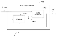
図2は、第2のクロック出力部102の内部構成の例を示すブロック図である。第2のクロック出力部102は、遅延回路111、位相同期回路112を備える。遅延回路111は、PDに基づいてCLK2を遅延させ、第5のクロック(以降、「CLK5」という。)として位相同期回路112へ出力する。
FIG. 2 is a block diagram illustrating an example of the internal configuration of the second
位相同期回路112は、入力される2系統のクロック、CLK0とCLK5の位相差がゼロになるように、CLK0を遅延させて、CLK2として出力する。あるいは、一般のPLLのように、位相同期回路112の内部に発振器を備え、CLK0とCLK5の位相差がゼロになるように、発振器を制御してもよい。
The
以上のように、第1の実施形態のクロック分配装置は、クロック分配部を経由して出力された2系統のクロックの位相差に基づいて、クロック分配部へ入力されるクロックの位相を変化させる。従って、クロック分配部を経由して出力された2系統のクロックの位相差を減少させることができる効果がある。
(第2の実施形態)
本発明の第2の実施形態について、図面を参照して詳細に説明する。図3は、第2の実施形態のクロック分配回路の構成を示す回路図である。本実施形態のクロック分配回路は、第1の実施形態のクロック分配装置の内部の回路構成を具体的に示すものである。
As described above, the clock distribution device according to the first embodiment changes the phase of the clock input to the clock distribution unit based on the phase difference between the two clocks output via the clock distribution unit. . Therefore, there is an effect that the phase difference between the two clocks output via the clock distribution unit can be reduced.
(Second Embodiment)
A second embodiment of the present invention will be described in detail with reference to the drawings. FIG. 3 is a circuit diagram showing a configuration of the clock distribution circuit according to the second embodiment. The clock distribution circuit of the present embodiment specifically shows the internal circuit configuration of the clock distribution device of the first embodiment.
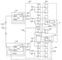
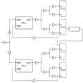
本実施形態のクロック分配回路は、第1のクロック出力部101、第2のクロック出力部102、第1のクロック分配部201、第2のクロック分配部202、位相差検出部300と、実動作回路501、実動作回路502を備える。
The clock distribution circuit according to this embodiment includes a first
第1のクロック出力部101は、PLL113を備える。第2のクロック出力部102は、PLL112、遅延回路111を備える。
The first
なお、図3のクロック分配回路の構成要素で、図1の第1の実施形態のクロック分配装置の各構成要素と同じ符号を付した構成要素は、第1の実施形態のものと同じ機能を備える。それらの構成要素についての説明は省略する。 Note that the constituent elements of the clock distribution circuit of FIG. 3 that have the same reference numerals as the constituent elements of the clock distribution apparatus of the first embodiment of FIG. 1 have the same functions as those of the first embodiment. Prepare. A description of these components is omitted.
第1のクロック分配部201、第2のクロック分配部202は、それぞれ、クロック・ツリーを構成する。第1のクロック分配部201、第2のクロック分配部202は、クロック・ドライバ203を備える。クロック・ドライバ203は、クロック信号の駆動能力を高めるために用いられるもので、信号の論理には影響を与えない。位相差検出部300は、D−フリップ・フロップ(以降、単に「F/F」という。)301を備える。
The first
本実施形態のクロック分配回路の回路構成について説明する。実動作回路501は、F/F503、504、論理回路505を含む。F/F503のデータ出力は論理回路505へ入力される。論理回路505の出力はF/F504のデータ入力に接続される。
The circuit configuration of the clock distribution circuit of this embodiment will be described. The
第1のクロック出力部101から出力されたCLK1は、クロック・ツリーの末端部で、CLK3として、F/F503のクロック入力、及び位相差検出部300のF/F301のデータ入力に接続される。第2のクロック出力部102から出力されたCLK2は、クロック・ツリーの末端部でCLK4として、F/F504のクロック入力、及び位相差検出部300のF/F301のクロック入力に接続される。
CLK1 output from the first
次に、本実施形態のクロック分配回路の動作について説明する。CLK1は、第1のクロック分配部201のクロック・ツリーによって分配され、CLK3となり、実動作回路501に到達する。同様に、CLK2は、第2のクロック分配部202のクロック・ツリーによって分配され、実動作回路502に到達する。
Next, the operation of the clock distribution circuit of this embodiment will be described. CLK1 is distributed by the clock tree of the first
第1のクロック出力部101は、外部から供給されるCLK0と、第1のクロック出力部101の出力から直接フィードバックしたCLK1の位相を比較する。そして、CLK1をCLK0に同期させる。このように、第1のクロック出力部101には、第1のクロック分配部201の末端部からのクロックがフィードバックされない。そのため、フィードバックされるクロックの、クロック・ジッターは大きく低減され、また、クロック・スキューも低減される。
The first
第2のクロック出力部102についても同様である。すなわち、外部から供給されるCLK0と、第2のクロック出力部102の出力からフィードバックしたCLK2の位相を比較し、CLK2をCLK0に同期させる。そのため、フィードバックされるクロックの、クロック・ジッターは大きく低減され、また、クロック・スキューも低減される。
The same applies to the second
F/F503はCLK3の立ち上がりエッジに同期して動作するので、論理回路505の出力もCLK3の立ち上がりエッジに同期して変化する。F/F504は、CLK3の立ち上がりエッジに同期して変化する論理回路505の出力を、CLK4の立ち上がりエッジに同期して保持する。
Since the F /
本クロック分配回路によるCLK2の位相制御が行われていない初期状態では、CLK3、CLK4の位相は一致しない可能性がある。なぜなら、第1のクロック分配部201、第2のクロック分配部202における、クロックの伝達遅延時間は必ずしも同じではないからである。そこで、本実施形態のクロック分配回路では、CLK3とCLK4の位相が一致するように、CLK2の位相を変化させる。
In the initial state where the phase control of CLK2 by the clock distribution circuit is not performed, the phases of CLK3 and CLK4 may not match. This is because the clock transmission delay times in the first
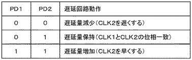
位相差検出部300を構成するF/F301は、CLK4の立ち上がりエッジに同期してCLK3を保持する。そのため、CLK4の立ち上がりタイミングに対して、CLK3の立ち上がりタイミングが遅いとき、F/F301の出力は0になる。逆に、CLK4の立ち上がりタイミングに対して、CLK3の立ち上がりタイミングが早いとき、F/F301の出力は1になる。つまり、F/F301の出力は、CLK4よりもCLK3の位相が遅れているとき0に、CLK4よりもCLK3の位相が進んでいるとき1になる。なお、F/F301の出力が、PDである。
The F /
PDが0、すなわち、CLK4よりもCLK3の位相が遅れている場合、CLK2の位相を遅らせることによって、CLK4の位相をCLK3の位相に近づけることができる。そこで、PDが0のとき、遅延回路111の遅延量を小さくし、CLK2の位相を遅らせる。
When PD is 0, that is, when the phase of CLK3 is delayed from CLK4, the phase of CLK4 can be brought close to the phase of CLK3 by delaying the phase of CLK2. Therefore, when PD is 0, the delay amount of the
PDが1、すなわち、CLK4よりもCLK3の位相が進んでいる場合、CLK2の位相を進めることによって、CLK4の位相をCLK3の位相に近づけることができる。そこで、PDが1のとき、遅延回路111の遅延量を大きくし、CLK2の位相を進める。
When PD is 1, that is, when the phase of CLK3 is ahead of CLK4, the phase of CLK4 can be brought close to the phase of CLK3 by advancing the phase of CLK2. Therefore, when PD is 1, the delay amount of
以上の遅延量の調整動作を繰り返すことによって、CLK3、CLK4の位相を近づけることができる。すなわち、CLK3とCLK4との間のクロック・スキューを低減することができる。 By repeating the above delay amount adjustment operation, the phases of CLK3 and CLK4 can be brought close to each other. That is, the clock skew between CLK3 and CLK4 can be reduced.
以上のように、本実施形態のクロック分配回路は、2系統のクロック分配部の、各々の末端部におけるクロックの位相差に基づいて、クロック分配部へ入力するクロックの位相を変化させる。従って、クロック分配部の末端部におけるクロックの位相差、すなわちクロック・スキューを低減できる効果がある。 As described above, the clock distribution circuit of the present embodiment changes the phase of the clock input to the clock distribution unit based on the phase difference between the clocks at the end portions of the two systems of the clock distribution unit. Therefore, there is an effect that the phase difference of the clock at the end of the clock distributor, that is, the clock skew can be reduced.
さらに、クロック分配部の末端部からクロック出力部までクロックをフィードバックすることがないので、フィードバックされるクロックの、クロック・ジッターを大幅に低減でき、クロック・スキューも低減できるという効果がある。
(第3の実施形態)
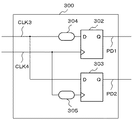
本発明の第3の実施形態について、図4、図5を用いて説明する。第3の実施形態のクロック分配回路は、クロック・スキューをさらに低減するために、第2の実施形態のクロック分配回路に、2系統のクロックを短絡させるスイッチ回路を追加したものである。図4は、本実施形態のクロック分配回路の末端部付近の回路構成を示す回路図である。クロック分配部の末端部は、図3のAで示した部分である。本実施形態のクロック分配回路のその他の構成要素は、第2の実施形態のクロック分配回路と同じである。
Further, since the clock is not fed back from the terminal portion of the clock distribution unit to the clock output unit, the clock jitter of the fed back clock can be greatly reduced, and the clock skew can be reduced.
(Third embodiment)
A third embodiment of the present invention will be described with reference to FIGS. The clock distribution circuit of the third embodiment is obtained by adding a switch circuit that short-circuits two clocks to the clock distribution circuit of the second embodiment in order to further reduce clock skew. FIG. 4 is a circuit diagram showing a circuit configuration near the end of the clock distribution circuit of this embodiment. The end of the clock distribution unit is the part indicated by A in FIG. Other components of the clock distribution circuit of this embodiment are the same as those of the clock distribution circuit of the second embodiment.
本実施形態のクロック分配回路は、図4に示すように、CLK3とCLK4のクロック・ライン間にスイッチ回路204を備える。スイッチ回路204は、スイッチ制御信号SWONによって制御される。スイッチ回路204の具体例としては、図5に示すような、トランスファー・ゲート205がある。トランスファー・ゲート205は、SWONが1のとき、CLK3のクロック・ラインとCLK4のクロック・ラインとを短絡する。そして、トランスファー・ゲート205は、SWONが0のとき、CLK3とCLK4とを開放状態とする。
As shown in FIG. 4, the clock distribution circuit of this embodiment includes a
本実施形態のクロック分配回路による制御が行われる前の初期状態では、2系統のクロックCLK3、CLK4の位相は一致していない可能性がある。そのため、初期状態では、SWONを0にし、CLK3のクロック・ラインとCLK4のクロック・ラインとのショートを防止する。そして、第2の実施形態で説明した制御によって、CLK3、CLK4の「位相調整が完了」した後、SWONを1にし、CLK3のクロック・ラインとCLK4のクロック・ラインを短絡する。
本実施形態のクロック分配回路においても、第1の実施形態で説明したように、CLK3とCLK4との位相差(第1の位相差)が正確にゼロになるとは限らない。しかし、第1の位相差は確実に低減される。「位相調整が完了」とは、第1の位相差がCLK2の位相調整機能によって、十分に低減された状態を意味する。
In the initial state before the control by the clock distribution circuit of this embodiment is performed, the phases of the two clocks CLK3 and CLK4 may not match. Therefore, in the initial state, SWON is set to 0 to prevent a short circuit between the clock line of CLK3 and the clock line of CLK4. Then, according to the control described in the second embodiment, after “phase adjustment is completed” of CLK3 and CLK4, SWON is set to 1, and the clock line of CLK3 and the clock line of CLK4 are short-circuited.
Also in the clock distribution circuit of this embodiment, as described in the first embodiment, the phase difference (first phase difference) between CLK3 and CLK4 is not always zero. However, the first phase difference is reliably reduced. “Phase adjustment is complete” means that the first phase difference is sufficiently reduced by the phase adjustment function of CLK2.
位相調整の完了は、例えば、CLK2の位相の調整が増加又は減少の一方向である状態から、逆の方向に変化したとき等をもって判断することができる。あるいは、CLK2の位相の調整を開始した後、所定の時間が経過したときに、第1の位相差の低減処理が完了したと判断することもできる。 Completion of the phase adjustment can be determined, for example, when the phase adjustment of CLK2 changes from one direction of increase or decrease to the opposite direction. Alternatively, it may be determined that the first phase difference reduction processing has been completed when a predetermined time has elapsed after starting the phase adjustment of CLK2.
本実施形態のクロック分配回路では、CLK3、CLK4の位相調整が完了した状態において、CLK3のクロック・ラインとCLK4のクロック・ラインを強制的に短絡する。従って、CLK3、CLK4の位相差はさらに低減される。 In the clock distribution circuit of this embodiment, the CLK3 clock line and the CLK4 clock line are forcibly short-circuited in a state where the phase adjustment of CLK3 and CLK4 is completed. Therefore, the phase difference between CLK3 and CLK4 is further reduced.
このように、スイッチ回路204は、CLK3とCLK4との位相差がある場合においても両方のクロック・ラインを強制的に短絡するので、オン抵抗は極力小さいことが望ましい。
Thus, since the
CLK3とCLK4は、F/F503、504、論理回路505等、実動作回路501、502へ供給される。CLK3とCLK4は、位相を強制的に一致させられているので、実動作回路501、502は確実な同期動作をすることができる。
CLK3 and CLK4 are supplied to
以上のように、第3の実施形態のクロック分配回路では、2系統のクロック間のクロック・スキューを低減した後、その2系統のクロックを強制的に短絡する。従って、クロックの位相調整によるクロック・スキューの低減の後、さらにそのクロック・スキューを低減することができるという効果がある。そして、クロック・スキューが存在する2系統のクロックを短絡させることがないという効果もある。
(第4の実施形態)
本発明の第4の実施形態について、図6を用いて説明する。第4の実施形態のクロック分配回路も、第3の実施形態と同様に、2系統のクロックを短絡させる短絡部を備える。そして、短絡部の直前にクロックの供給を停止するクロック停止回路を備える。図6は、本実施形態のクロック分配回路の末端部付近の回路構成を示す回路図である。クロック分配部の末端部は、図3のAで示した部分である。本実施形態のクロック分配回路のその他の構成要素は、第2の実施形態のクロック分配回路と同じである。
As described above, in the clock distribution circuit according to the third embodiment, after the clock skew between the two clocks is reduced, the two clocks are forcibly short-circuited. Therefore, after the clock skew is reduced by adjusting the phase of the clock, the clock skew can be further reduced. Also, there is an effect that the two clocks having clock skew are not short-circuited.
(Fourth embodiment)
A fourth embodiment of the present invention will be described with reference to FIG. Similarly to the third embodiment, the clock distribution circuit according to the fourth embodiment also includes a short-circuit unit that short-circuits two clocks. A clock stop circuit for stopping the supply of the clock is provided immediately before the short-circuit portion. FIG. 6 is a circuit diagram showing a circuit configuration near the end of the clock distribution circuit of this embodiment. The end of the clock distribution unit is the part indicated by A in FIG. Other components of the clock distribution circuit of this embodiment are the same as those of the clock distribution circuit of the second embodiment.
本実施形態のクロック分配回路は、図6に示すように、CLK3、CLK4のそれぞれの信号線にANDゲート506、507が挿入されている。そして、クロック供給許可信号CLKONによって、ANDゲート506、507の後段の回路へのクロックの供給を制御する。ANDゲート506、507の出力は短絡されている。
In the clock distribution circuit of the present embodiment, AND
CLKONが0のとき、ANDゲート506、507の出力は、共に0固定となる。CLKONが1のとき、ANDゲート506、507は、それぞれCLK3、CLK4を出力する。そして、CLK3とCLK4はショートされ、F/F503、504、論理回路505等、実動作回路501、502へ供給される。CLK3とCLK4は、位相を強制的に一致させられているので、実動作回路501、502は確実な同期動作をすることができる。
When CLKON is 0, the outputs of the AND
なお、本実施形態のクロック分配回路による制御が行われる前の初期状態においては、CLK3、CLK4の位相は一致していない可能性がある。そのため、初期状態では、CLKONを0にし、ANDゲート506、507の出力同士がショートしないように制御する。従って、CLK3とCLK4との間にクロック・スキューが存在した状態では、CLK3とCLK4とは短絡されることがない。そして、第2の実施形態で説明した制御によって、CLK3、CLK4の「位相調整が完了」した後、CLKONを1にし、CLK3、CLK4をショートする。「位相調整が完了」の意味は、第3の実施形態で説明したとおりである。位相調整の完了の判断方法も、第3の実施形態で説明したとおりである。
In the initial state before the control by the clock distribution circuit of this embodiment is performed, the phases of CLK3 and CLK4 may not match. Therefore, in the initial state, CLKON is set to 0 and control is performed so that the outputs of the AND
以上のように、第4の実施形態のクロック分配回路でも、2系統のクロック間のクロック・スキューを低減した後、その2系統のクロックを強制的に短絡する。従って、クロックの位相調整によるクロック・スキューの低減の後、さらにそのクロック・スキューを低減することができるという効果がある。 As described above, even in the clock distribution circuit of the fourth embodiment, after the clock skew between the two clocks is reduced, the two clocks are forcibly short-circuited. Therefore, after the clock skew is reduced by adjusting the phase of the clock, the clock skew can be further reduced.
そして、クロックの位相調整によるクロック・スキューの低減前には、クロックの短絡部へのクロックの供給を停止する。そのため、クロック・スキューが存在する2系統のクロックを短絡させることがないという効果もある。
(第5の実施形態)
本発明の第5の実施形態について、図7、図8を用いて説明する。第5の実施形態のクロック分配回路は、位相差検出部の位相差検出機能に、2系統のクロックの位相が一致していることの検出機能を追加したものである。図7は、本実施形態のクロック分配回路の、位相差検出部の回路構成を示す回路図である。図8は、図7の位相差検出部の出力の各組み合わせに対する、遅延回路の動作の対応を示す表である。
Then, before the clock skew is reduced by the clock phase adjustment, the supply of the clock to the short-circuit portion of the clock is stopped. Therefore, there is also an effect that the two clocks having clock skew are not short-circuited.
(Fifth embodiment)
A fifth embodiment of the present invention will be described with reference to FIGS. The clock distribution circuit according to the fifth embodiment is obtained by adding a detection function that the phases of two clocks are coincident to the phase difference detection function of the phase difference detection unit. FIG. 7 is a circuit diagram showing a circuit configuration of the phase difference detection unit of the clock distribution circuit of this embodiment. FIG. 8 is a table showing the correspondence of the operation of the delay circuit to each combination of outputs of the phase difference detection unit of FIG.
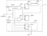
本実施形態の位相差検出部300は、図7に示すように、F/F302、303、遅延素子304、305を備える。F/F302のデータ入力にはCLK3を遅延素子304で遅延させて入力し、F/F302のクロック入力にはCLK4を遅延させずに入力する。F/F303のデータ入力にはCLK3を遅延させずに入力し、F/F303のクロック入力にはCLK4を遅延素子304で遅延させて入力する。なお、F/F302、303の出力の組み合わせが、位相差信号PDに相当する。以降、F/F302、303の出力をそれぞれ、PD1、PD2という。
As illustrated in FIG. 7, the phase
PD1、PD2の値と、遅延回路の制御との組み合わせを図8に示す。CLK3の位相がCLK4の位相より遅い場合、PD1、PD2は共に0となる。このとき、CLK4の位相を遅らせるように遅延回路111の遅延量を小さくし、CLK2の位相を遅らせる。
A combination of the values of PD1 and PD2 and the control of the delay circuit is shown in FIG. When the phase of CLK3 is later than the phase of CLK4, both PD1 and PD2 are 0. At this time, the delay amount of the
CLK3の位相がCLK4の位相より早い場合、PD1、PD2は、共に1となる。このときは、逆にCLK4の位相を進めるように遅延回路111の遅延量を大きくし、CLK2の位相を進める。
When the phase of CLK3 is earlier than the phase of CLK4, PD1 and PD2 are both 1. At this time, the delay amount of the
以上の遅延量の調整動作を繰り返すことによって、CLK3とCLK4の位相を近づけることができる。すなわち、CLK3とCLK4のクロック・スキューを低減することができる。以上の、CLK2の位相調整によるクロック・スキューの低減機能については、第2の実施形態と同じである。 By repeating the above delay amount adjustment operation, the phases of CLK3 and CLK4 can be brought close to each other. That is, the clock skew between CLK3 and CLK4 can be reduced. The clock skew reduction function by the CLK2 phase adjustment is the same as that of the second embodiment.
第5の実施形態の位相検出部300は、CLK3とCLK4の位相が一致していることの検出機能を備える。すなわち、CLK3、CLK4の位相が一致しているとき、PD1は0、PD2は1になるので、位相の一致を検出することができる。このときは、遅延回路111の遅延量はそのときの値で保持される。
The
CLK3とCLK4の位相が一致していることを検出する機能を備えなければ、位相が一致しているにもかかわらず、絶えずクロックの位相調整を続けることとなる。従って、CLK3とCLK4との間にクロック・スキューが発生する。さらに、CLK3とCLK4の位相の進み・遅れの関係が絶えず逆転する現象も引き起こされる。この場合は、スキューの存在自体だけでなく、論路回路のタイミング設計のマージンが不足するという問題もある。 If the function of detecting that the phases of CLK3 and CLK4 are in agreement is not provided, the phase adjustment of the clock is continued even though the phases are in agreement. Therefore, a clock skew occurs between CLK3 and CLK4. Furthermore, a phenomenon in which the relationship between the phase advance and delay of CLK3 and CLK4 is constantly reversed is also caused. In this case, there is a problem that not only the presence of the skew itself but also a margin for timing design of the logical circuit is insufficient.
しかし、第5の実施形態のクロック分配回路は、CLK3とCLK4の位相が一致しているときには位相の調整を停止する。そのため、上記のような問題は発生しない。そして、再び位相差が生じた場合は、第5の実施形態のクロック分配回路は位相の調整を再開し、位相が一致するように制御する。 However, the clock distribution circuit of the fifth exemplary embodiment stops the phase adjustment when the phases of CLK3 and CLK4 coincide. Therefore, the above problem does not occur. When the phase difference occurs again, the clock distribution circuit according to the fifth embodiment resumes the phase adjustment and performs control so that the phases match.
以上のように、第5の実施形態のクロック分配回路の位相検出部は、2系統のクロックの位相が一致していることの検出機能を備える。そのため、クロックの位相の変更を継続することによる、クロック・スキューの発生が防止される。従って、第2、第3の実施形態のクロック分配回路と比較して、さらにクロック・スキューを低減できるという効果がある。 As described above, the phase detection unit of the clock distribution circuit according to the fifth embodiment has a function of detecting that the phases of the two clocks are in agreement. Therefore, the occurrence of clock skew caused by continuing to change the clock phase is prevented. Therefore, the clock skew can be further reduced as compared with the clock distribution circuits of the second and third embodiments.
また、2系統のクロック間の位相の進み・遅れの関係が逆転する現象は発生しない。そのため、論路回路のタイミング設計のマージンが不足するという問題の発生を防止することができるという効果もある。
(第6の実施形態)
本発明の第6の実施形態について、図9、図10を用いて説明する。第6の実施形態のクロック分配回路も、第5の実施形態のクロック分配回路と同様に、位相差検出部の位相差検出機能に、2系統のクロックの位相が一致していることの検出機能を追加したものである。図9は、本実施形態のクロック分配回路の、位相差検出部の回路構成を示す回路図である。図10は、図9の位相差検出部の出力の各組み合わせに対する、遅延回路の動作の対応を示す表である。
In addition, a phenomenon in which the phase advance / delay relationship between the two clocks is reversed does not occur. Therefore, there is also an effect that it is possible to prevent the occurrence of a problem that a margin for timing design of the logical circuit is insufficient.
(Sixth embodiment)
A sixth embodiment of the present invention will be described with reference to FIGS. Similarly to the clock distribution circuit of the fifth embodiment, the clock distribution circuit of the sixth embodiment also has a function of detecting that the phases of the two systems of clocks coincide with the phase difference detection function of the phase difference detection unit. Is added. FIG. 9 is a circuit diagram illustrating a circuit configuration of the phase difference detection unit of the clock distribution circuit according to the present embodiment. FIG. 10 is a table showing the correspondence of the operation of the delay circuit to each combination of outputs of the phase difference detection unit of FIG.
本実施形態の位相差検出部300は、図9に示すように、F/F306、307、308、309、遅延素子310、311、312、313、ORゲート314、ANDゲート315を備える。
As illustrated in FIG. 9, the phase
F/F306のデータ入力にはCLK3を遅延素子310で遅延させて入力し、F/F306のクロック入力にはCLK4を遅延させずに入力する。F/F307のデータ入力にはCLK4を遅延素子311で遅延させて入力し、F/F307のクロック入力にはCLK3を遅延させずに入力する。F/F308のデータ入力にはCLK3を遅延させずに入力し、F/F308のクロック入力には、CLK4を遅延素子312で遅延させて入力する。F/F309のデータ入力にはCLK4を遅延させずに入力し、F/F309のクロック入力にはCLK3を遅延素子313で遅延させて入力する。
CLK3 is delayed by the
そして、F/F306の出力及びF/F307の反転出力をORゲート314に入力し、F/F308の出力及びF/F309の反転出力をANDゲート315に入力する。ORゲート314、ANDゲート315の出力の組み合わせが、位相差信号PDに相当する。以降、ORゲート314、ANDゲート315の出力をそれぞれ、PD3、PD4という。
Then, the output of the F /
なお、F/F306、307、308、309間のタイミング特性の差、遅延素子310、311、312、313間のタイミング特性の差は、それぞれ、無視できることが望ましい。特性差が無視できるとき、CLK3に同期して動作するF/Fの出力とCLK4に同期して動作するF/Fの出力は、同じタイミングで変化するので、位相差検出部300の出力の誤動作を少なくすることができる。
It should be noted that the difference in timing characteristics between the F /
本実施形態の位相差検出部300の動作について説明する。PD3、PD4の値と、遅延回路の制御との組み合わせを図10に示す。CLK3の位相がCLK4より遅い場合、PD3、PD4は、共に0となる。このとき、CLK4の位相を遅らせるように、遅延回路111の遅延量を小さくし、CLK2の位相を遅らせる。
The operation of the phase
CLK3の位相がCLK4の位相より早い場合、PD3、PD4は、共に1となる。このときは、逆にCLK4の位相を進めるように、遅延回路111の遅延量を大きくし、CLK2の位相を進める。
When the phase of CLK3 is earlier than the phase of CLK4, both PD3 and PD4 are 1. At this time, the delay amount of the
以上の遅延量の調整動作を繰り返すことによって、CLK3とCLK4の位相を近づけることができる。すなわち、CLK3とCLK4のクロック・スキューを低減することができる。以上の、CLK2の位相調整によるクロック・スキューの低減機能については、第2の実施形態と同じである。 By repeating the above delay amount adjustment operation, the phases of CLK3 and CLK4 can be brought close to each other. That is, the clock skew between CLK3 and CLK4 can be reduced. The clock skew reduction function by the CLK2 phase adjustment is the same as that of the second embodiment.
第6の実施形態の位相検出部300は、第5の実施形態の位相検出部300と同様に、CLK3とCLK4の位相が一致していることの検出機能を備える。すなわち、CLK3、CLK4の位相が一致しているとき、PD3は1、PD4は0になるので、位相の一致を検出することができる。このときは、遅延回路111の遅延量はそのときの値で保持される。
Similar to the
CLK3とCLK4の位相が一致していることの検出機能を備えない場合の問題、及び第6の実施形態のクロック分配回路によってその問題が解決できる理由は、第5の実施形態で説明した内容と同じである。 The problem in the case of not having the function of detecting that the phases of CLK3 and CLK4 coincide with each other and the reason that the problem can be solved by the clock distribution circuit of the sixth embodiment are the same as the contents described in the fifth embodiment. The same.
以上のように、第6の実施形態のクロック分配回路の位相検出部は、2系統のクロックの位相が一致していることの検出機能を備える。そのため、クロックの位相の変更を継続することによる、クロック・スキューの発生が防止される。従って、第2、第3の実施形態のクロック分配回路と比較して、さらにクロック・スキューを低減できるという効果がある。 As described above, the phase detection unit of the clock distribution circuit according to the sixth embodiment has a function of detecting that the phases of the two clocks are the same. Therefore, the occurrence of clock skew caused by continuing to change the clock phase is prevented. Therefore, the clock skew can be further reduced as compared with the clock distribution circuits of the second and third embodiments.
また、2系統のクロック間の位相の進み・遅れの関係が逆転する現象は発生しない。そのため、論路回路のタイミング設計のマージンが不足するという問題の発生を防止することができるという効果もある。 In addition, a phenomenon in which the phase advance / delay relationship between the two clocks is reversed does not occur. Therefore, there is also an effect that it is possible to prevent the occurrence of a problem that a margin for timing design of the logical circuit is insufficient.
なお、第5及び第6の実施形態の説明から明らかなように、本発明の位相差検出部には、各種の位相比較器を適用することができる。位相比較器は、第2乃至第4の実施形態のように、位相差の極性のみを検出できるもの、あるいは、第5、第6の実施形態のように、位相差の有無及び極性を検出できるものの、いずれも本発明に適用可能である。 As is apparent from the descriptions of the fifth and sixth embodiments, various phase comparators can be applied to the phase difference detection unit of the present invention. The phase comparator can detect only the polarity of the phase difference as in the second to fourth embodiments, or can detect the presence and absence of the phase difference and the polarity as in the fifth and sixth embodiments. However, any of them can be applied to the present invention.
また、遅延回路111の挿入位置は、第2のクロック出力部102内のクロックのフィードバック・ラインに限られない。遅延回路111の挿入位置は、CLK1とCLK2の相対的な位相関係を調整することができる位置であれば、他の位置でも差し支えない。遅延回路111の挿入位置は、例えば、第1のクロック出力部101内のPLL113の、基準クロックCLK0の入力ライン、あるいはフィードバック・ラインでもよい。あるいは、遅延回路111の挿入位置は、第2のクロック出力部102内のPLL112の基準クロックCLK0の入力ラインでもよい。いずれの位置に遅延回路111を設けてもCLK1とCLK2の相対的な位相関係を調整することができるので、本発明の動作を実現することができる。
The insertion position of the
なお、以上の実施形態は各々他の実施形態と組み合わせることができる。例えば、第3又は第4の実施形態のクロック間の短絡と、第5又は第6の実施形態の位相差検出部の改良を組み合わせることができる。 Each of the above embodiments can be combined with other embodiments. For example, the short circuit between the clocks of the third or fourth embodiment can be combined with the improvement of the phase difference detection unit of the fifth or sixth embodiment.
101 第1のクロック出力部
102 第2のクロック出力部
111 遅延回路
201 第1のクロック分配部
202 第2のクロック分配部
203 クロック・ドライバ
204 スイッチ回路
205 トランスファー・ゲート
300 位相差検出部
301、302、303 フリップ・フロップ(F/F)
304、305 遅延素子
306、307、308、309 フリップ・フロップ(F/F)
310、311、312、313 遅延素子
314 ORゲート
315 ANDゲート
501、502 実動作回路
503、504 フリップ・フロップ(F/F)
505 論理回路
506、507 ANDゲート
CLK0 基準クロック
CLK1 第1のクロック
CLK2 第2のクロック
CLK3 第3のクロック
CLK4 第4のクロック
CLK5 遅延第2のクロック
PD、PD1、PD2、PD3、PD4 位相差信号
SWON スイッチ制御信号
CLKON クロック供給許可信号
DESCRIPTION OF
304, 305
310, 311, 312, 313
505
Claims (8)
前記基準クロックに同期した第2のクロックを出力する第2のクロック出力部と、
前記第1のクロックが供給される第1のクロック分配部の第1の分岐点から分岐させた第3のクロックと、前記第2のクロックが供給される第2のクロック分配部の第2の分岐点から分岐させた第4のクロックとの位相差である、第1の位相差を検出する位相差検出部と、
前記第3のクロックを供給する第1の配線と前記第4のクロックを供給する第2の配線を短絡させるクロック短絡部とを備え、
前記位相差検出部は、前記第1の位相差に基づいて、前記第3のクロックの位相と前記第4のクロックの位相が等しい同相状態を検出し、
前記第2のクロック出力部は、
前記第2のクロックを、前記第1の位相差に基づいた第1の遅延時間だけ遅延させ第1の帰還クロックとして出力する第1の遅延回路と、
前記基準クロックと前記第1の帰還クロックとの位相差を制御することによって前記基準クロックに同期させた前記第2のクロックを出力する第1の位相同期回路を備え、
前記第1の位相差が小さくなるように、前記基準クロックと前記第2のクロックとの間に前記第1の位相差に基づく第2の位相差を設定し、
前記同相状態であるとき前記第1の遅延時間を保持し、
前記短絡部は、前記同相状態であるとき、前記第1の配線と前記第2の配線とを短絡させる
ことを特徴とするクロック分配装置。 A first clock output unit for outputting a first clock synchronized with a reference clock;
A second clock output unit for outputting a second clock synchronized with the reference clock;
A third clock branched from a first branch point of the first clock distribution unit to which the first clock is supplied, and a second clock of the second clock distribution unit to which the second clock is supplied A phase difference detection unit for detecting a first phase difference, which is a phase difference with a fourth clock branched from the branch point;
And a clock shorting portion for shorting the second wiring for supplying the fourth clock and the first wiring for supplying the third clock,
The phase difference detection unit detects an in-phase state in which the phase of the third clock and the phase of the fourth clock are equal based on the first phase difference;
The second clock output unit includes:
A first delay circuit that delays the second clock by a first delay time based on the first phase difference and outputs the second clock as a first feedback clock;
A first phase synchronization circuit that outputs the second clock synchronized with the reference clock by controlling a phase difference between the reference clock and the first feedback clock;
Setting a second phase difference based on the first phase difference between the reference clock and the second clock so that the first phase difference is small;
Holding the first delay time when in the in-phase state;
The said short circuit part short-circuits the said 1st wiring and the said 2nd wiring when it is the said in-phase state, The clock distribution apparatus characterized by the above-mentioned.
ことを特徴とする請求項1記載のクロック分配装置。 2. The first delay circuit increases or decreases the first delay time by setting a time smaller than a predetermined allowable phase difference set as the first phase difference as a step. The clock distribution device described.
前記第2のクロック出力部は、前記進相状態であるとき前記第1の遅延時間を増加させ、前記遅相状態であるとき前記第1の遅延時間を減少させる
ことを特徴とする請求項1又は2記載のクロック分配装置。 The phase difference detection unit includes a phase advance state in which the first phase difference indicates that the phase of the fourth clock is ahead of the phase of the third clock, and the first phase difference is Detecting a lagging state indicating that the phase of the fourth clock is delayed from the phase of the third clock;
2. The second clock output unit increases the first delay time when in the advanced phase state and decreases the first delay time when in the delayed phase state. Or the clock distribution apparatus of 2.
前記基準クロックに、前記第2の位相差に基づいた第2の遅延時間だけ遅延させ遅延基準クロックとして出力する第2の遅延回路と、
前記遅延基準クロックと前記第2のクロックとの位相差を制御することによって前記基準クロックに同期させた前記第2のクロックを出力する位相同期回路を備える
ことを特徴とする請求項1乃至5のいずれかに記載のクロック分配装置。 The second clock output unit includes:
A second delay circuit that delays the reference clock by a second delay time based on the second phase difference and outputs the delayed clock as a delayed reference clock;
6. The phase synchronization circuit according to claim 1, further comprising: a phase synchronization circuit that outputs the second clock synchronized with the reference clock by controlling a phase difference between the delayed reference clock and the second clock. The clock distribution device according to any one of the above.
ことを特徴とする請求項1乃至6のいずれかに記載のクロック分配装置。 The first clock output unit feeds back the first clock as a second feedback clock to the input, and synchronizes with the reference clock by controlling a phase difference between the reference clock and the second feedback clock. 7. The clock distribution device according to claim 1, further comprising a second phase synchronization circuit that outputs the first clock.
前記第1の位相差に基づいて、前記第3のクロックの位相と前記第4のクロックの位相が等しい同相状態を検出する同相状態検出工程と、
前記第2のクロックを、前記第1の位相差に基づいた第1の遅延時間だけ遅延させ第1の帰還クロックとして出力する第1の遅延工程と、
前記基準クロックと前記第1の帰還クロックとの位相差を制御することによって前記基準クロックに同期させた前記第2のクロックを出力する第1の位相同期工程と、
前記基準クロックと前記第2のクロックとの間に、前記第1の位相差に基づく第2の位相差を、前記第1の位相差が小さくなるように設定する位相差設定行程と、
前記同相状態であるとき前記第1の遅延時間を保持する遅延時間保持行程と、
前記同相状態であるとき、前記第1のクロックを供給する第1の配線と前記第2のクロックを供給する第2の配線とを短絡させるクロック短絡工程
を備えることを特徴とするクロック分配方法。 A third clock branched from the first branch point of the first clock distribution unit supplied with the first clock synchronized with the reference clock, and a second clock supplied with the second clock synchronized with the reference clock. A phase difference detection step of detecting a first phase difference with the fourth clock branched from the second branch point of the two clock distribution units;
An in-phase state detecting step of detecting an in-phase state in which the phase of the third clock and the phase of the fourth clock are equal based on the first phase difference;
A first delay step of delaying the second clock by a first delay time based on the first phase difference and outputting as a first feedback clock;
A first phase synchronization step of outputting the second clock synchronized with the reference clock by controlling a phase difference between the reference clock and the first feedback clock;
A phase difference setting step of setting a second phase difference based on the first phase difference between the reference clock and the second clock so that the first phase difference becomes small;
A delay time holding step for holding the first delay time when in the in-phase state;
A clock distribution method comprising: a clock short-circuiting step of short-circuiting a first wiring for supplying the first clock and a second wiring for supplying the second clock when in the in-phase state.
Priority Applications (2)
| Application Number | Priority Date | Filing Date | Title |
|---|---|---|---|
| JP2009069411A JP4862906B2 (en) | 2009-03-23 | 2009-03-23 | Clock distribution apparatus and clock distribution method |
| US12/716,345 US20100237914A1 (en) | 2009-03-23 | 2010-03-03 | Clock distribution device and clock distribution method |
Applications Claiming Priority (1)
| Application Number | Priority Date | Filing Date | Title |
|---|---|---|---|
| JP2009069411A JP4862906B2 (en) | 2009-03-23 | 2009-03-23 | Clock distribution apparatus and clock distribution method |
Publications (2)
| Publication Number | Publication Date |
|---|---|
| JP2010224717A JP2010224717A (en) | 2010-10-07 |
| JP4862906B2 true JP4862906B2 (en) | 2012-01-25 |
Family
ID=42737003
Family Applications (1)
| Application Number | Title | Priority Date | Filing Date |
|---|---|---|---|
| JP2009069411A Expired - Fee Related JP4862906B2 (en) | 2009-03-23 | 2009-03-23 | Clock distribution apparatus and clock distribution method |
Country Status (2)
| Country | Link |
|---|---|
| US (1) | US20100237914A1 (en) |
| JP (1) | JP4862906B2 (en) |
Families Citing this family (11)
| Publication number | Priority date | Publication date | Assignee | Title |
|---|---|---|---|---|
| JP5568057B2 (en) | 2011-05-30 | 2014-08-06 | 株式会社東芝 | Memory access circuit and memory system |
| JP6111739B2 (en) * | 2013-03-01 | 2017-04-12 | 日本電気株式会社 | Clock skew correction circuit, correction method thereof, and clock distribution device |
| JP2015015572A (en) * | 2013-07-04 | 2015-01-22 | 日本電気株式会社 | Oscillation circuit, oscillation device and oscillation method |
| JP6263906B2 (en) * | 2013-08-28 | 2018-01-24 | 富士通株式会社 | Electronic circuit and control method |
| US9613679B2 (en) * | 2014-11-14 | 2017-04-04 | Cavium, Inc. | Controlled dynamic de-alignment of clocks |
| US9601181B2 (en) * | 2014-11-14 | 2017-03-21 | Cavium, Inc. | Controlled multi-step de-alignment of clocks |
| US9577648B2 (en) * | 2014-12-31 | 2017-02-21 | Semtech Corporation | Semiconductor device and method for accurate clock domain synchronization over a wide frequency range |
| US9256246B1 (en) * | 2015-01-29 | 2016-02-09 | Qualcomm Incorporated | Clock skew compensation with adaptive body biasing in three-dimensional (3D) integrated circuits (ICs) (3DICs) |
| US10054635B2 (en) * | 2016-05-09 | 2018-08-21 | Hamilton Sunstrand Corporation | Integrated system and method for testing system timing margin |
| US10110205B2 (en) * | 2016-09-07 | 2018-10-23 | International Business Machines Corporation | Method and apparatus for clock skew control with low jitter in an integrated circuit |
| CN111459878B (en) * | 2020-04-02 | 2023-05-23 | 京微齐力(北京)科技有限公司 | Method and system for automatically reducing clock delay deviation |
Family Cites Families (11)
| Publication number | Priority date | Publication date | Assignee | Title |
|---|---|---|---|---|
| JPH0476610A (en) * | 1990-07-13 | 1992-03-11 | Hitachi Ltd | Clock distributing system |
| JPH06276089A (en) * | 1993-03-23 | 1994-09-30 | Fujitsu General Ltd | Pll circuit |
| JPH07281783A (en) * | 1994-04-04 | 1995-10-27 | Mitsubishi Electric Corp | Semiconductor integrated circuit device |
| JP2867967B2 (en) * | 1996-07-26 | 1999-03-10 | 日本電気株式会社 | PLD with clock skew adjustment function |
| JP2004159239A (en) * | 2002-11-08 | 2004-06-03 | Renesas Technology Corp | Semiconductor integrated circuit |
| JP4020836B2 (en) * | 2003-07-23 | 2007-12-12 | シャープ株式会社 | Clock tree circuit and semiconductor integrated circuit device |
| US7368961B2 (en) * | 2005-12-22 | 2008-05-06 | Rambus Inc. | Clock distribution network supporting low-power mode |
| JP2007336003A (en) * | 2006-06-12 | 2007-12-27 | Nec Electronics Corp | Clock distribution circuit, forming method thereof, semiconductor integrated circuit, and program thereof |
| KR100837278B1 (en) * | 2007-02-27 | 2008-06-11 | 삼성전자주식회사 | Clock skew controller and integrated circuit including the same |
| JP2008219216A (en) * | 2007-03-01 | 2008-09-18 | Fujitsu Ltd | Clock supply unit |
| US7872512B2 (en) * | 2008-04-01 | 2011-01-18 | Altera Corporation | Robust time borrowing pulse latches |
-
2009
- 2009-03-23 JP JP2009069411A patent/JP4862906B2/en not_active Expired - Fee Related
-
2010
- 2010-03-03 US US12/716,345 patent/US20100237914A1/en not_active Abandoned
Also Published As
| Publication number | Publication date |
|---|---|
| US20100237914A1 (en) | 2010-09-23 |
| JP2010224717A (en) | 2010-10-07 |
Similar Documents
| Publication | Publication Date | Title |
|---|---|---|
| JP4862906B2 (en) | Clock distribution apparatus and clock distribution method | |
| US8942333B2 (en) | Apparatus and methods for clock alignment for high speed interfaces | |
| US9030242B2 (en) | Data output timing control circuit for semiconductor apparatus | |
| KR100954117B1 (en) | Delay Locked Loop Apparatus | |
| US7622969B2 (en) | Methods, devices, and systems for a delay locked loop having a frequency divided feedback clock | |
| US8373462B2 (en) | Delay lock loop and delay lock method | |
| US20020079937A1 (en) | Digital delay locked loop with wide dynamic range and fine precision | |
| EP2518629A1 (en) | Signal receiving circuit, memory controller, processor, computer, and phase control method | |
| US8766688B2 (en) | DLL circuit and delay-locked method using the same | |
| US20100090738A1 (en) | Circuit and Method for Clock Skew Compensation in Voltage Scaling | |
| JP2004145999A (en) | Timing adjustment circuit and semiconductor device provided with it | |
| US7242737B2 (en) | System and method for data phase realignment | |
| JP5417688B2 (en) | Semiconductor integrated circuit | |
| KR100560644B1 (en) | Clock synchronizing circuit for use in an integrated circuit device | |
| WO1999004528A1 (en) | A method and apparatus for synchronizing a control signal | |
| KR100838376B1 (en) | DLL circuit capable of preventing malfunctioning caused by VDD change. | |
| US7152008B2 (en) | Calibrated differential voltage crossing | |
| JP2006333472A (en) | Delay lock loop, and delay chain setting method | |
| TWI806487B (en) | System for signal alignment | |
| US9721627B2 (en) | Method and apparatus for aligning signals | |
| US8638137B2 (en) | Delay locked loop | |
| KR20120111074A (en) | Internal clock genertor and operating method thereof | |
| KR20080001124A (en) | Semiconductor memory device | |
| JP4381880B2 (en) | Timing adjustment circuit | |
| JP2010171826A (en) | Controller for memory module |
Legal Events
| Date | Code | Title | Description |
|---|---|---|---|
| A131 | Notification of reasons for refusal |
Free format text: JAPANESE INTERMEDIATE CODE: A131 Effective date: 20110208 |
|
| A521 | Written amendment |
Free format text: JAPANESE INTERMEDIATE CODE: A523 Effective date: 20110408 |
|
| RD01 | Notification of change of attorney |
Free format text: JAPANESE INTERMEDIATE CODE: A7421 Effective date: 20110705 |
|
| A131 | Notification of reasons for refusal |
Free format text: JAPANESE INTERMEDIATE CODE: A131 Effective date: 20110726 |
|
| A521 | Written amendment |
Free format text: JAPANESE INTERMEDIATE CODE: A523 Effective date: 20110921 |
|
| TRDD | Decision of grant or rejection written | ||
| A01 | Written decision to grant a patent or to grant a registration (utility model) |
Free format text: JAPANESE INTERMEDIATE CODE: A01 Effective date: 20111011 |
|
| A01 | Written decision to grant a patent or to grant a registration (utility model) |
Free format text: JAPANESE INTERMEDIATE CODE: A01 |
|
| A61 | First payment of annual fees (during grant procedure) |
Free format text: JAPANESE INTERMEDIATE CODE: A61 Effective date: 20111024 |
|
| FPAY | Renewal fee payment (event date is renewal date of database) |
Free format text: PAYMENT UNTIL: 20141118 Year of fee payment: 3 |
|
| R150 | Certificate of patent or registration of utility model |
Free format text: JAPANESE INTERMEDIATE CODE: R150 |
|
| LAPS | Cancellation because of no payment of annual fees |