JP4824920B2 - Group III element nitride crystal semiconductor device - Google Patents
Group III element nitride crystal semiconductor device Download PDFInfo
- Publication number
- JP4824920B2 JP4824920B2 JP2004299311A JP2004299311A JP4824920B2 JP 4824920 B2 JP4824920 B2 JP 4824920B2 JP 2004299311 A JP2004299311 A JP 2004299311A JP 2004299311 A JP2004299311 A JP 2004299311A JP 4824920 B2 JP4824920 B2 JP 4824920B2
- Authority
- JP
- Japan
- Prior art keywords
- substrate
- semiconductor device
- thin film
- film layer
- layer
- Prior art date
- Legal status (The legal status is an assumption and is not a legal conclusion. Google has not performed a legal analysis and makes no representation as to the accuracy of the status listed.)
- Expired - Fee Related
Links
Images


Description
本発明は、III族元素窒化物結晶半導体デバイスに関する。 The present invention relates to a group III element nitride crystal semiconductor device.
窒化ガリウム(GaN)などのIII族元素窒化物化合物半導体(以下、III族元素窒化物半導体またはGaN系半導体という場合がある)は、緑色や青色、紫外光を発光する半導体素子の材料として注目されている。青色レーザダイオード(LD)は、高密度光ディスクやディスプレイに応用され、また青色発光ダイオード(LED)はディスプレイや照明などに応用される。また、紫外線LDはバイオテクノロジーなどへの応用が期待され、紫外線LEDは蛍光灯の紫外線源として期待されている。 Group III element nitride compound semiconductors such as gallium nitride (GaN) (hereinafter sometimes referred to as Group III element nitride semiconductors or GaN-based semiconductors) are attracting attention as materials for semiconductor elements that emit green, blue, and ultraviolet light. ing. Blue laser diodes (LD) are applied to high-density optical discs and displays, and blue light-emitting diodes (LEDs) are applied to displays and lighting. Further, ultraviolet LD is expected to be applied to biotechnology and the like, and ultraviolet LED is expected to be an ultraviolet light source for fluorescent lamps.
LDやLED用のIII族元素窒化物半導体(例えば、GaN)の基板は、通常、サファイア基板上に、気相エピタキシャル成長法を用いてIII族元素窒化物結晶をヘテロエピタキシャル成長させることによって形成されている。この方法で得られる結晶の転位密度は、通常、108cm-2〜109cm-2であり、転位密度の減少が重要な課題となっている。また、この課題を解決するために、転位密度を低減する取り組みが行われており、例えばELOG(Epitaxial lateral overgrowth)法が開発されている。この方法によれば、転位密度を105cm-2〜106cm-2程度まで下げることができるが、作製工程が複雑である。 A group III element nitride semiconductor (for example, GaN) substrate for LD or LED is usually formed by heteroepitaxially growing a group III element nitride crystal on a sapphire substrate using a vapor phase epitaxial growth method. . The dislocation density of the crystal obtained by this method is usually 10 8 cm −2 to 10 9 cm −2 , and reduction of the dislocation density is an important issue. In order to solve this problem, efforts have been made to reduce the dislocation density. For example, an ELOG (Epitaxial lateral overgrowth) method has been developed. According to this method, the dislocation density can be lowered to about 10 5 cm −2 to 10 6 cm −2, but the manufacturing process is complicated.
一方、気相エピタキシャル成長ではなく、液相で結晶成長を行う方法も検討されてきた。しかしながら、GaNやAlNなどのIII族元素窒化物単結晶の融点における窒素の平衡蒸気圧は10000atm(10000×1.013×105Pa)以上であるため、従来、GaNを液相で成長させるためには1200℃で8000atm(8000×1.013×105Pa)の条件が必要とされてきた。これに対し、近年、Naフラックスを用いることで、750℃、50atm(50×1.013×105Pa)という比較的低温低圧でGaNを合成できることが明らかにされた。 On the other hand, a method of performing crystal growth in a liquid phase instead of vapor phase epitaxial growth has been studied. However, since the equilibrium vapor pressure of nitrogen at the melting point of a group III element nitride single crystal such as GaN or AlN is 10000 atm (10000 × 1.013 × 10 5 Pa) or more, conventionally, GaN is grown in the liquid phase. Has required a condition of 8000 atm (8000 × 1.013 × 10 5 Pa) at 1200 ° C. On the other hand, it has recently been clarified that GaN can be synthesized at a relatively low temperature and low pressure of 750 ° C. and 50 atm (50 × 1.013 × 10 5 Pa) by using Na flux.
最近では、アンモニアを含む窒素ガス雰囲気下においてGaとNaとの混合物を800℃、50atm(50×1.013×105Pa)で溶融させ、この融液を用いて96時間の育成時間で、最大結晶サイズが1.2mm程度の単結晶が得られている(例えば、特許文献1参照)。 Recently, a mixture of Ga and Na was melted at 800 ° C. and 50 atm (50 × 1.013 × 10 5 Pa) in a nitrogen gas atmosphere containing ammonia, and this melt was used for a growth time of 96 hours. A single crystal having a maximum crystal size of about 1.2 mm is obtained (see, for example, Patent Document 1).
また、サファイア基板上に有機金属気相成長(MOCVD:Metalorganic Chemical Vapor Deposition)法によってGaN結晶層を成膜したのち、液相成長(LPE:Liquid Phase Epitaxy)法によって単結晶を成長させる方法も報告されている。
アルカリ金属およびアルカリ土類金属の少なくとも一方をフラックスとして用いた窒化物結晶の液相成長方法においても、不純物の混入が問題となる。不純物が入ると、キャリア密度などが変化する場合があるからである。また、フラックスであるアルカリ金属やアルカリ土類金属は、半導体プロセスにおいて、特に混入が嫌われる元素類である。 Also in the liquid crystal growth method of a nitride crystal using at least one of an alkali metal and an alkaline earth metal as a flux, mixing of impurities becomes a problem. This is because the carrier density and the like may change when impurities are introduced. Moreover, alkali metals and alkaline earth metals, which are fluxes, are elements that are particularly apt to be mixed in semiconductor processes.
そこで、本発明の目的は、アルカリ金属およびアルカリ土類金属の少なくとも一方をフラックスとし、この中でIII族元素窒化物結晶を成長させた基板を用いて作製した半導体デバイスにおいて、不純物の拡散を防止する技術を提供することである。 Accordingly, an object of the present invention is to prevent diffusion of impurities in a semiconductor device manufactured using a substrate on which at least one of an alkali metal and an alkaline earth metal is used as a flux and a group III element nitride crystal is grown therein. Is to provide technology to do.
前記目的を達成するために、本発明のIII族元素窒化物結晶半導体デバイスは、III族元素窒化物結晶基板上にIII族元素窒化物結晶層が積層された半導体デバイスであって、前記基板が、アルカリ金属およびアルカリ土類金属の少なくとも一方を含む融解液(フラックス)中において、窒素含有ガスの窒素とIII族元素とを反応させて結晶化させることにより製造されたものであり、前記基板上に、薄膜層が形成されており、前記薄膜層における前記基板中の不純物の拡散係数が、前記基板における前記基板中の不純物の拡散係数よりも小さいことを特徴とする半導体デバイスである。 In order to achieve the above object, a group III element nitride crystal semiconductor device of the present invention is a semiconductor device in which a group III element nitride crystal layer is laminated on a group III element nitride crystal substrate, In the melt (flux) containing at least one of an alkali metal and an alkaline earth metal, it is produced by reacting nitrogen of a nitrogen-containing gas with a group III element to cause crystallization, and on the substrate In addition, a thin film layer is formed, and the diffusion coefficient of impurities in the substrate in the thin film layer is smaller than the diffusion coefficient of impurities in the substrate in the substrate.
本発明の半導体デバイスでは、III族元素窒化物結晶基板上に、薄膜層が形成され、前記薄膜層における前記基板中の不純物の拡散係数が、前記基板における前記拡散係数よりも小さいため、前記基板中の不純物がIII族元素窒化物結晶層に拡散することを防止できる。 In the semiconductor device of the present invention, a thin film layer is formed on a group III element nitride crystal substrate, and the diffusion coefficient of impurities in the substrate in the thin film layer is smaller than the diffusion coefficient in the substrate. It is possible to prevent impurities therein from diffusing into the group III element nitride crystal layer.
アルカリ金属およびアルカリ土類金属の少なくとも一方を含むフラックス中でIII族元素窒化物結晶を成長させて得られた結晶の一部に、例えば、貫通転位(例えば、らせん転位や刃状転位等)や格子欠陥等が存在する場合は、そこにアルカリ金属やアルカリ土類金属等が混入するおそれがある。この混入したアルカリ金属やアルカリ土類金属等の拡散を防止できるのが、本発明の特徴である。なお、結晶中の貫通転位や格子欠陥領域に、アルカリ金属やアルカリ土類金属、中でも、NaおよびLiが混入するおそれがあり、これが拡散することは、本発明者等が初めて見出したものである。この混入は、例えば、SIMS(Secondary ion mass spectroscopy)により確認できる。また、基板に電子線を照射することによるカソードルミネッセンスを観察し、それにより得られた暗点の部分を、転位部分とした。 In part of the crystal obtained by growing a group III element nitride crystal in a flux containing at least one of an alkali metal and an alkaline earth metal, for example, threading dislocation (for example, screw dislocation or edge dislocation) In the case where there are lattice defects or the like, alkali metal or alkaline earth metal may be mixed therein. It is a feature of the present invention that diffusion of the mixed alkali metal, alkaline earth metal, etc. can be prevented. Note that the present inventors have found for the first time that alkali metals and alkaline earth metals, especially Na and Li, may be mixed in the threading dislocations and lattice defect regions in the crystal, and that this diffuses. . This contamination can be confirmed by, for example, SIMS (Secondary ion mass spectroscopy). Moreover, the cathodoluminescence by irradiating an electron beam to a board | substrate was observed, and the part of the dark spot obtained by that was made into the dislocation part.
本発明において、III族元素窒化物結晶基板は、アルカリ金属およびアルカリ土類金属の少なくとも一方を含む融解液(フラックス)中において、窒素含有ガスの窒素とIII族元素とを反応させて結晶化させたものであればよい。例えば、前記融解液中で大型のバルク状に成長させたIII族元素窒化物結晶をスライス加工したものを前記基板として使用してもよい。 In the present invention, a group III element nitride crystal substrate is crystallized by reacting nitrogen of a nitrogen-containing gas with a group III element in a melt (flux) containing at least one of an alkali metal and an alkaline earth metal. Anything can be used. For example, a substrate obtained by slicing a group III element nitride crystal grown in a large bulk in the melt may be used as the substrate.
前記アルカリ金属としては、Na、Li、K、Rb、CsおよびFrがあげられ、前記アルカリ土類金属としては、Ca、Mg、Sr、BeおよびBaがあげられる。これらは、単独で使用しても2種類以上で併用してもよい。これらの中でもNa、Li、Ca、Mgを使用することが好ましく、特にNaとLiとを併用することや、NaやLiを単体で使用することが好ましい。前記基板が、例えば、GaN基板である場合、NaとLiとを併用することが好ましく、AlN基板である場合、Li、NaおよびSnから選択される1つと、Caとを併用することが好ましい。また、前記融解液は、フラックス成分として、アルカリ金属やアルカリ土類金属に加えて、その他の金属を含んでいてもよい。前記金属としては、例えば、Sn等があげられる。 Examples of the alkali metal include Na, Li, K, Rb, Cs and Fr, and examples of the alkaline earth metal include Ca, Mg, Sr, Be and Ba. These may be used alone or in combination of two or more. Among these, it is preferable to use Na, Li, Ca, and Mg, and it is particularly preferable to use Na and Li together or to use Na or Li alone. For example, when the substrate is a GaN substrate, it is preferable to use Na and Li together. When the substrate is an AlN substrate, it is preferable to use Ca together with one selected from Li, Na, and Sn. In addition to the alkali metal or alkaline earth metal, the melt may contain other metals as a flux component. Examples of the metal include Sn.
前記III族元素としては、Ga、Al、Inがあげられ、好ましくはGaおよびAlであり、前記基板の組成式が、AluGavIn1-u-vN(ただし0≦u≦1、0≦v≦1、u+v≦1)で表されることが好ましい。また、前記III族元素がGaであり、前記基板がGaNであることや、前記III族元素がAlであり、前記基板がAlNであることが好ましい。 Examples of the group III element include Ga, Al, and In, preferably Ga and Al, and the composition formula of the substrate is Al u Ga v In 1 -uv N (where 0 ≦ u ≦ 1, 0 ≦ It is preferable that v ≦ 1, u + v ≦ 1). The group III element is preferably Ga, the substrate is GaN, the group III element is Al, and the substrate is preferably AlN.
また、前記基板は、予め準備した支持基板の上にIII族元素窒化物結晶を成長させたものであってもよい。この場合において、前記支持基板の上にシード層が形成されており、前記シード層が、前記III族元素窒化物結晶基板と同じ組成の結晶から形成されたものが好ましい。前記支持基板は、表面が(111)面であるGaAs基板、表面が(111)面であるSi基板、表面が(0001)面であるサファイア基板および表面が(0001)面であるSiC基板のいずれかの基板であることが好ましい。 The substrate may be one obtained by growing a group III element nitride crystal on a support substrate prepared in advance. In this case, a seed layer is preferably formed on the support substrate, and the seed layer is preferably formed of a crystal having the same composition as the group III element nitride crystal substrate. The support substrate may be any one of a GaAs substrate having a (111) surface, a Si substrate having a (111) surface, a sapphire substrate having a (0001) surface, and a SiC substrate having a (0001) surface. Such a substrate is preferable.
本発明において、前記基板中の不純物としては、例えば、フラックス成分であるアルカリ金属やアルカリ土類金属、結晶の製造に使用する坩堝、反応容器、その他の部材等の構成材料成分に由来するもの等があげられる。前記アルカリ金属としては、Na、Li、K、Rb、CsおよびFrがあげられ、前記アルカリ土類金属としては、Ca、Mg、Sr、BeおよびBaがあげられる。この中でも、特に、Na、Li、Ca、Mg等が前記基板中に混入することにより、例えば、III族元素窒化物結晶層のキャリア密度等に大きな影響を与えるおそれがある。 In the present invention, the impurities in the substrate include, for example, alkali metals and alkaline earth metals that are flux components, those derived from constituent material components such as crucibles, reaction vessels, and other members used for producing crystals, etc. Can be given. Examples of the alkali metal include Na, Li, K, Rb, Cs and Fr, and examples of the alkaline earth metal include Ca, Mg, Sr, Be and Ba. Among these, in particular, Na, Li, Ca, Mg, etc. may be mixed into the substrate, which may have a great influence on the carrier density of the group III element nitride crystal layer, for example.
本発明において、前記薄膜層における前記基板中の不純物の拡散係数が、前記基板における前記基板中の不純物の拡散係数よりも小さければよく、例えば、前記基板における前記基板中の不純物の拡散係数よりも1桁以上小さいことが好ましい。また、前記薄膜層における前記基板中の不純物の拡散係数は、例えば、1000℃で、1×10-16cm2/sec以下であることが好ましく、1×10-17cm2/sec以下であることがより好ましい。前記不純物の拡散係数は、SIMSにより評価できる。SIMSによる評価方法としては、例えば、まず、SIMSにより基板内の不純物を分析し、次に、基板表面にイオン注入によりイオンを注入し、さらに所定の温度で熱処理を施した後、さらにSIMSにより基板内の不純物を分析し、処理前後のSIMSの分析結果をもとに不純物のプロファイルを作成することにより、前記不純物の拡散係数を求めることができる。 In the present invention, the diffusion coefficient of impurities in the substrate in the thin film layer only needs to be smaller than the diffusion coefficient of impurities in the substrate in the substrate, for example, the diffusion coefficient of impurities in the substrate in the substrate. It is preferably one digit or more smaller. In addition, the diffusion coefficient of impurities in the substrate in the thin film layer is preferably 1 × 10 −16 cm 2 / sec or less at 1000 ° C., for example, and is 1 × 10 −17 cm 2 / sec or less. It is more preferable. The impurity diffusion coefficient can be evaluated by SIMS. As an evaluation method by SIMS, for example, first, impurities in the substrate are analyzed by SIMS, then ions are implanted into the substrate surface by ion implantation, and further subjected to a heat treatment at a predetermined temperature, and then the substrate is further simulated by SIMS. The impurity diffusion coefficient of the impurity can be obtained by analyzing the impurity in the substrate and creating an impurity profile based on the SIMS analysis results before and after the treatment.
前記薄膜層としては、例えば、窒化シリコン(SiN)、窒化アルミニウム(AlN)、窒化アルミニウムガリウム(AlxGa1-xN(ただし、0<x<1))、炭化シリコン(SiC)、窒化ゲルマニウム(GeN2)、ダイヤモンドライクカーボン、ダイヤモンド等があげられ、好ましくは窒化シリコン、窒化アルミニウムガリウム、窒化アルミニウムであり、より好ましくは窒化アルミニウムガリウムである。また、前記基板として、バルク結晶から形成されたIII族元素窒化物結晶基板を使用する場合、薄膜層が窒化アルミニウムであることが好ましい。
Examples of the thin film layer include silicon nitride (SiN), aluminum nitride (AlN), aluminum gallium nitride (Al x Ga 1-x N (where 0 <x <1 )), silicon carbide (SiC), and germanium nitride. Examples thereof include (GeN 2 ), diamond-like carbon, diamond, and the like, preferably silicon nitride, aluminum gallium nitride, and aluminum nitride, and more preferably aluminum gallium nitride. Further, when a group III element nitride crystal substrate formed from a bulk crystal is used as the substrate, the thin film layer is preferably aluminum nitride.
前記基板が、例えば、GaN基板である場合、薄膜層が窒化シリコン(SiN)、窒化アルミニウム(AlN)、窒化アルミニウムガリウム(AlxGa1-xN(ただし、0<x<1))および炭化シリコン(SiC)の少なくとも一つであることが好ましく、より好ましくは窒化アルミニウムガリウム、窒化アルミニウムであり、特に好ましくは窒化アルミニウムガリウムである。前記基板が、例えば、AlN基板である場合、薄膜層がダイヤモンドであることが好ましい。 When the substrate is a GaN substrate, for example, the thin film layer is silicon nitride (SiN), aluminum nitride (AlN), aluminum gallium nitride (Al x Ga 1-x N (where 0 <x <1 )) and carbonization. It is preferably at least one of silicon (SiC), more preferably aluminum gallium nitride and aluminum nitride, and particularly preferably aluminum gallium nitride. For example, when the substrate is an AlN substrate, the thin film layer is preferably diamond.
前記薄膜層の厚みは、特に限定されず、例えば、1nm〜1000nmであり、好ましくは5nm〜100nmであり、より好ましくは10nm〜50nmである。前記薄膜層が窒化シリコンである場合、その厚みが5nm以下であることが好ましく、3nm以下であることが好ましい。厚みが5nm以下であれば、前記薄膜層上にIII族元素窒化物結晶の成長が妨害されない。 The thickness of the thin film layer is not particularly limited, and is, for example, 1 nm to 1000 nm, preferably 5 nm to 100 nm, and more preferably 10 nm to 50 nm. When the thin film layer is silicon nitride, the thickness is preferably 5 nm or less, and preferably 3 nm or less. If the thickness is 5 nm or less, the growth of the group III element nitride crystal on the thin film layer is not hindered.
前記薄膜層の形成方法は、特に制限されず、形成材料に応じて適宜決定すればよく、例えば、電子サイクロトロン共鳴(ECR)スパッタ法、MOCVD法等があげられる。例えば、窒化シリコン層を形成する場合、電子サイクロトロン共鳴(ECR)スパッタ法が好ましく、窒化アルミニウム層を形成する場合、減圧MOCVD法が好ましい。 The method for forming the thin film layer is not particularly limited, and may be appropriately determined depending on the forming material. Examples thereof include an electron cyclotron resonance (ECR) sputtering method and an MOCVD method. For example, when forming a silicon nitride layer, an electron cyclotron resonance (ECR) sputtering method is preferable, and when forming an aluminum nitride layer, a low pressure MOCVD method is preferable.
前記結晶層は、その組成式が、AluGavIn1-u-vN(ただし0≦u≦1、0≦v≦1、u+v≦1)で表されることが好ましく、例えば、MOCVD法等の気相成長法により形成することが好ましい。 The composition of the crystal layer is preferably represented by Al u Ga v In 1-uv N (where 0 ≦ u ≦ 1, 0 ≦ v ≦ 1, u + v ≦ 1), for example, MOCVD method or the like It is preferable to form by the vapor phase growth method.
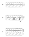
次に、本発明の半導体デバイスの構成について、図1(a)〜(c)を例にとり説明する。 Next, the configuration of the semiconductor device of the present invention will be described with reference to FIGS.
図1(a)に示すように、本発明の半導体デバイスは、III族元素窒化物結晶基板13上に、薄膜層15と、III族元素窒化物結晶層18とが形成されており、基板13の表面全体に、薄膜層15が形成されていることが好ましい。
As shown in FIG. 1A, in the semiconductor device of the present invention, a
また、図1(b)に示すように、III族元素窒化物結晶基板13に、貫通転位14が存在する場合、薄膜層15が、貫通転位14に対応する部分に形成されていればよい。前述のように、貫通転位14の領域には、不純物が存在するおそれがあるので、これに対応する部分に薄膜層15を形成することにより、基板13中の不純物がIII族元素窒化物結晶層18に拡散することを十分防止できる。
In addition, as shown in FIG. 1B, when threading
また、図1(c)に示すように、本発明の半導体デバイスは、III族元素窒化物結晶基板13と薄膜層15との間に、さらに、III族元素窒化物結晶層18が形成されていてもよい。
Further, as shown in FIG. 1C, in the semiconductor device of the present invention, a group III element
また、本発明の半導体デバイスは、前記基板上に形成された前記薄膜層とともに、若しくは前記薄膜層に代えてその側面に薄膜層が形成されていてもよい。また、前記半導体デバイスが複数に分割されたチップであってもよく、この場合、前記基板表面の薄膜層と共に、若しくは前記薄膜層に代えて、前記チップ側面に薄膜層が形成されていることが好ましい。このように側面に薄膜層を形成することにより、分割すること等により露出したチップの側面から、例えば、アルカリ金属等の不純物が拡散することも防止できる。 In the semiconductor device of the present invention, a thin film layer may be formed on the side surface together with the thin film layer formed on the substrate or instead of the thin film layer. The semiconductor device may be a chip divided into a plurality of parts. In this case, a thin film layer is formed on the side surface of the chip together with the thin film layer on the substrate surface or instead of the thin film layer. preferable. By forming the thin film layer on the side surface in this manner, it is possible to prevent impurities such as alkali metals from diffusing from the side surface of the chip exposed by dividing or the like.
本発明の半導体デバイスは、レーザダイオード、発光ダイオードまたは電界効果トランジスタであることが好ましい。 The semiconductor device of the present invention is preferably a laser diode, a light emitting diode, or a field effect transistor.
本発明の半導体デバイスの製造方法の一例を、図2を用いて説明する。なお、図1と同一箇所には同一の符号を付している。 An example of a method for manufacturing a semiconductor device of the present invention will be described with reference to FIG. In addition, the same code | symbol is attached | subjected to the same location as FIG.
まず、図2(a)に示すように、サファイア基板等の支持基板11上に、組成式AluGavIn1-u-vN(ただし0≦u≦1、0≦v≦1、u+v≦1)で表されるシード層12を形成する。シード層12は、種結晶となり、例えば、GaNや、AluGa1-uN(ただし、0≦u≦1)等で表される結晶であることが好ましい。シード層12は、例えば、MOCVD法、MBE法、HVPE法などにより形成できる。支持基板11には、例えば、表面が(111)面であるGaAs基板、表面が(111)面であるSi基板、表面が(0001)面であるサファイア基板、または表面が(0001)面であるSiC基板を用いることができる。なお、支持基板11とシード層12との間に他の半導体層を含んでもよい。
First, as shown in FIG. 2A, a composition formula Al u Ga v In 1-uv N (where 0 ≦ u ≦ 1, 0 ≦ v ≦ 1, u + v ≦ 1) is formed on a
次に、図2(b)に示すように、窒素を含む雰囲気中(好ましくは100atm(100×1.013×105Pa)以下の加圧雰囲気)において、アルカリ金属およびアルカリ土類金属の少なくとも一方とIII族元素と窒素とを含む融解液にシード層12を接触させ、シード層12上にLPE−GaN13aを成長させる。この場合、支持基板11、シード層12およびLPE−GaN13aを含めてIII族元素窒化物結晶基板13とする。なお、LPE−GaN13aを形成後、前記支持基板11を除去してもよく、除去することにより、LPE−GaN13a内の歪みを緩和できる。除去方法としては、例えば、レーザリフトオフ法、研削加工、研磨加工等があげられる。
Next, as shown in FIG. 2B, in an atmosphere containing nitrogen (preferably a pressurized atmosphere of 100 atm (100 × 1.013 × 10 5 Pa) or less), at least alkali metal and alkaline earth metal are used. One
前記III族元素としては、Ga、Al、Inがあげられ、好ましくはGaおよびAlである。アルカリ金属およびアルカリ土類金属は、通常、フラックスとして機能し、前記アルカリ金属としては、Na、Li、K、Rb、CsおよびFrがあげられ、前記アルカリ土類金属としては、Ca、Mg、Sr、BeおよびBaがあげられ、これらのうちの少なくとも1つ、すなわち、これらの1つまたはこれらの混合物が用いられる。窒素を含む雰囲気下としては、例えば、窒素ガスや、アンモニアガスの少なくとも一方を含む窒素含有ガス雰囲気を適用できる。 Examples of the group III element include Ga, Al, and In, and Ga and Al are preferable. Alkaline metals and alkaline earth metals usually function as flux, and the alkali metals include Na, Li, K, Rb, Cs, and Fr, and the alkaline earth metals include Ca, Mg, Sr. , Be and Ba, at least one of which is used, ie one of these or a mixture thereof. As the atmosphere containing nitrogen, for example, a nitrogen-containing gas atmosphere containing at least one of nitrogen gas and ammonia gas can be applied.
融解液は、例えば、材料を坩堝に投入して加熱することによって調製される。融解液を調製したのち、融解液を過飽和の状態とすることによってIII族元素窒化物結晶を成長させる。材料の溶融および結晶成長は、例えば、温度が700℃〜1100℃程度で、圧力が1atm(1×1.013×105Pa)〜50atm(50×1.013×105Pa)程度で行うことができる。この方法によれば、組成式AlxGayIn1-x-yN(ただし0≦x≦1、0≦y≦1、x+y≦1)で表されるIII族元素窒化物結晶、例えば、GaNや、組成式AlxGa1-xN(ただし0≦x≦1)で表される結晶が得られる。 The melt is prepared, for example, by putting the material into a crucible and heating. After preparing the melt, the group III element nitride crystal is grown by bringing the melt into a supersaturated state. The melting and crystal growth of the material are performed, for example, at a temperature of about 700 ° C. to 1100 ° C. and a pressure of about 1 atm (1 × 1.013 × 10 5 Pa) to 50 atm (50 × 1.013 × 10 5 Pa). be able to. According to this method, a group III element nitride crystal represented by a composition formula Al x Ga y In 1-xy N (where 0 ≦ x ≦ 1, 0 ≦ y ≦ 1, x + y ≦ 1), for example, GaN or Thus, a crystal represented by a composition formula Al x Ga 1-x N (where 0 ≦ x ≦ 1) is obtained.
図2(c)に示すように、液相成長させたLPE−GaN13a中には、いくつかの貫通転位14が存在するおそれがある。特に、選択的に成長させる場合には、選択的に形成されたシード層から基板の厚み方向に向かって貫通転位14(例えば、らせん転位や刃状転位など)が存在するおそれがあり、この貫通転位14の領域には、フラックス成分やその他不純物が多数存在する可能性がある。したがって、貫通転位14が存在する部分には、液相成長させたLPE−GaN13aの上部に、例えば、窒化シリコン等の薄膜層15を形成する。これにより、例えば、LPE−GaN13aからのナトリウム金属等の拡散を防止できる。この薄膜層15は、例えば、電子サイクロトロン共鳴(ECR)スパッタ法を用いて形成できる。
As shown in FIG. 2C, some threading
そして、図2(d)のように、例えば、MOCVD法によりGaN層16やAlGaN層17を形成することにより、半導体レーザ、発光ダイオードや高周波デバイスなどのデバイス構造を形成することで、信頼性の高い半導体デバイスを実現できる。
Then, as shown in FIG. 2D, for example, by forming the
また、III族元素窒化物結晶基板13としてGaN基板を使用し、その上に薄膜層15として、電子サイクロトロン共鳴(ECR)スパッタ法により窒化シリコン層や(例えば、厚み3nm)や、MOCVD法によりAlN層を形成してもよい(例えば、厚み100nm)。なお、前記MOCVD法によるAlN層の形成は、減圧MOCVD法を適用することが好ましい。そして、薄膜層15上に、例えば、基板温度が約1020℃〜1100℃になるように基板を加熱したのち、トリメチルガリウム(TMG)とNH3とを基板上に供給することによってn型GaN結晶を形成できる。n型GaN結晶上に、半導体レーザ、発光ダイオードや高周波デバイスなどのデバイス構造を形成することで、信頼性の高い半導体デバイスを実現できる。このように薄膜層として窒化シリコン層や窒化アルミニウム層を形成することにより、III族元素窒化物結晶基板13中に存在するナトリウム等の不純物が結晶層16に拡散することを防止できる。
Further, a GaN substrate is used as the group III element
以下、実施例を用いて本発明をさらに詳細に説明する。なお、以下の実施例ではGaN結晶を用いたIII族元素窒化物半導体デバイスの作製について説明するが、例えば、AlxGa1-xNやAlN等の組成式AlxGayIn1-x-yN(ただし、0≦x≦1、0≦y≦1、x+y≦1)で表されるIII族元素窒化物結晶も同様の方法によって形成できる。 Hereinafter, the present invention will be described in more detail with reference to examples. In the following examples, the fabrication of a group III element nitride semiconductor device using a GaN crystal will be described. For example, the composition formula Al x Ga y In 1 -xy N such as Al x Ga 1-x N or AlN is used. A group III element nitride crystal represented by (where 0 ≦ x ≦ 1, 0 ≦ y ≦ 1, x + y ≦ 1) can also be formed by a similar method.
実施例1は、選択的に形成したシード層上に液相成長法で成長させIII族元素窒化物結晶を用いて、半導体デバイスを作製する例である。 Example 1 is an example in which a semiconductor device is manufactured using a group III element nitride crystal grown by a liquid phase growth method on a selectively formed seed layer.
まず、図3(a)のように、サファイアからなる支持基板21の温度を約1020℃〜1100℃になるように加熱したのち、トリメチルガリウム(TMG)とNH3とを基板上に供給することによって、GaNからなる半導体シード層22を形成した。
First, as shown in FIG. 3A, the temperature of the
次に、フォトリソグラフィーによって、半導体シード層22の表面上にレジストパターンを形成する。次に、図3(b)に示すように、Cl2ガスを用いたドライエッチングによって、半導体シード層22をパターン処理する。前記ドライエッチングは、誘導結合型の反応性ドライエッチング(RIE)装置を用いて行うことができる。
Next, a resist pattern is formed on the surface of the
次に、レジストパターンを除去して、半導体シード層22を形成する。なお、半導体シード層22の側面および支持基板21面に、マスクを形成しておいてもよい。そして、窒素雰囲気下(好ましくは100atm(100×1.013×105Pa)以下の加圧雰囲気下)において、GaとNaと窒素とを含む融解液に、半導体シード層22の表面を接触させ、融解液を過飽和状態で維持することによって、図3(c)に示すように、半導体シード層22上に選択的にLPE−GaN23aを成長させる。この場合、支持基板21、半導体シード層22およびLPE−GaN23aを含めてIII族元素窒化物結晶基板23とする。
Next, the resist pattern is removed, and the
図4にIII族元素窒化物結晶の作製に使用する揺動型LPE装置の一例を示す。この揺動型LPE装置300は、ステンレス製の育成炉301を備え、50atm(50×1.013×105Pa)の気圧に耐えられるようになっている。育成炉301には、加熱用のヒータ302および熱電対303が配置されている。坩堝固定台304は育成炉301内に配置されており、これには、回転軸305を中心に回転する機構が取り付けられている。坩堝固定台304内には、窒化ホウ素(BN)またはアルミナ(Al2O3)からなる坩堝306が固定されている。坩堝306内には、融解液307および種結晶308が配置される。坩堝固定台304が回転することにより、坩堝306内の融解液が左右に移動し、これにより、融解液を攪拌することができる。雰囲気圧力は、流量調整器309によって調整される。原料ガスである窒素ガス、またはアンモニアガス(NH3ガス)と窒素ガスとの混合ガスは、原料ガスタンク(図示せず)から供給され、ガス精製部によって不純物が除去されたのちに育成炉301内に送られる。
FIG. 4 shows an example of an oscillating LPE apparatus used for producing a group III element nitride crystal. The
以下、この装置を用いた結晶成長の一例について説明する。 Hereinafter, an example of crystal growth using this apparatus will be described.
(1)まず、GaとフラックスであるNaとを、所定の量だけ秤量し、坩堝内にセットする。Gaには、純度が99.9999%(シックスナイン)以上のものを用い、Naは、精製したNaを用いることが好ましい。He(N2、Ar、Ne、Xeなどでもよい)置換したグローブボックス内でNaを加熱して融解し、表面層に現れる酸化物などを除去することによってNaを精製できる。ゾーンリファイニング法によってNaを精製してもよい。ゾーンリファイニング法では、チューブ内でNaの融解と固化とを繰り返すことによって、不純物を析出させ、それを除去することによってNaの純度を上げることができる。 (1) First, Ga and Na which is a flux are weighed by a predetermined amount and set in a crucible. Ga having a purity of 99.9999% (six nines) or more is preferably used, and purified Na is preferably used. Na can be purified by heating and melting Na in a substituted glove box (which may be N 2 , Ar, Ne, Xe, etc.) to remove oxides and the like appearing on the surface layer. Na may be purified by a zone refining method. In the zone refining method, impurities are precipitated by repeating melting and solidification of Na in a tube, and the purity of Na can be increased by removing it.
(2)次に、坩堝内の原材料を融解するため、電気炉内の温度を800℃まで上昇させる。この段階では、図示するように、種結晶基板は融解液中には存在しない。GaおよびNaをかき混ぜるため、種結晶基板上に融解液が付着しない程度に、坩堝を揺動させる。GaNの酸化を防止するため、雰囲気ガスとしては、例えば、窒素ガスを用いることが好ましい。 (2) Next, in order to melt the raw material in the crucible, the temperature in the electric furnace is raised to 800 ° C. At this stage, as shown, the seed crystal substrate is not present in the melt. In order to mix Ga and Na, the crucible is swung so that the melt does not adhere to the seed crystal substrate. In order to prevent GaN oxidation, for example, nitrogen gas is preferably used as the atmospheric gas.
(3)次に、回転軸を中心に坩堝を回転させ種結晶基板を融解液中に入れ、結晶育成を開始させる。 (3) Next, the crucible is rotated around the rotation axis, the seed crystal substrate is placed in the melt, and crystal growth is started.
(4)結晶育成中は、融解液を攪拌させるため、1分間に1周期のスピードで坩堝を揺動させる。ただし、育成中は種結晶基板は融解液中に存在させ、坩堝を800℃に保持し、圧力を40atm(40×1.013×105Pa)に保持し、例えば、10時間LPE成長を行う。 (4) During crystal growth, the crucible is swung at a speed of one cycle per minute in order to stir the melt. However, during the growth, the seed crystal substrate is present in the melt, the crucible is kept at 800 ° C., the pressure is kept at 40 atm (40 × 1.013 × 10 5 Pa), and, for example, LPE growth is performed for 10 hours. .
(5)育成終了後は、図示するように坩堝を回転させ、融解液中から基板を取り出し、融解液温度を降下させる。 (5) After the growth is completed, the crucible is rotated as shown in the figure, the substrate is taken out of the melt, and the melt temperature is lowered.
上記方法でGaN結晶を成長させたところ、半導体シード層22から結晶成長が開始され、半導体シード層から基板表面に向かって貫通転位が観測されたが、半導体シード層からラテラル(横方向)成長した部分は、良好なGaN単結晶が育成できた。また、ラテラル成長したGaN結晶同士がぶつかる部分にも転位が観測された。
When the GaN crystal was grown by the above method, crystal growth was started from the
この方法によれば、Naのみならず、Li、K、Ca、Sr、Baフラックス、またはアルカリ金属とアルカリ土類金属との混合フラックスを用いても、同様の効果が得られる。例えば、NaとCaとの混合フラックスでは、Caを10%程度混入することで、より低圧での結晶育成が可能となる。 According to this method, not only Na but also Li, K, Ca, Sr, Ba flux, or mixed flux of alkali metal and alkaline earth metal can be used to obtain the same effect. For example, in a mixed flux of Na and Ca, it is possible to grow crystals at a lower pressure by mixing about 10% of Ca.
LPE−GaN23a中には、前述のように、半導体シード層22から基板表面に向かって貫通転位24が観測された。また、ラテラル成長したGaN結晶同士がぶつかる部分にも転位が観測された。SIMSにより、不純物分析を行ったところ、貫通転位24領域には、例えば、ナトリウムなどの不純物が多く存在した。そのため、図3(d)に示すように、例えば、貫通転位24が存在する領域の基板23の表面に窒化シリコンからなる薄膜層25を電子サイクロトロン共鳴(ECR)スパッタ法により形成した。前記薄膜層は、窒化シリコンに代えて、窒化アルミニウム、窒化アルミニウムガリウム、炭化シリコン、窒化ゲルマニウム、炭化シリコン、ダイヤモンドライクカーボンであってもよい。なお、基板23の表面は、機械加工(研磨加工)とメカノケミカル研磨により、平坦化加工してもよい。
As described above, threading
そして、図3(e)に示すように、例えば、MOCVD法によりGaN層26およびAlGaN層27を形成することにより本発明の半導体デバイスを作製することができる。アルカリ金属フラックス法により作製されたGaN基板を用いて半導体デバイスを作製する際、このように薄膜層25を形成することにより、半導体レーザや発光ダイオードの発光部や、FETトランジスタの各電極部へのアルカリ金属などの拡散を防止できるため、デバイスの特性を向上することができる。
And as shown in FIG.3 (e), the semiconductor device of this invention is producible by forming the
半導体シード層が形成された基板を用いてGaN結晶をLPE成長させたGaN基板について説明したが、GaN結晶をシードとして大型バルク成長させた結晶をスライス加工して得られたGaN基板を使用してもよい。このように成長させた結晶は、選択的に成長していないため、ランダムに発生する転位部分などにアルカリ金属やアルカリ土類金属等の不純物を含むおそれがある。そのため、基板表面全体に薄膜層を形成することで、不純物の拡散を防止できる。 Although a GaN substrate obtained by LPE growth of a GaN crystal using a substrate on which a semiconductor seed layer is formed has been described, a GaN substrate obtained by slicing a crystal obtained by growing a large bulk using a GaN crystal as a seed Also good. Since crystals grown in this manner are not selectively grown, there is a possibility that impurities such as alkali metals and alkaline earth metals may be contained in randomly generated dislocations. Therefore, diffusion of impurities can be prevented by forming a thin film layer over the entire substrate surface.
次に、電界効果トランジスタを作製する方法について図5に基づき説明する。III族窒化物結晶基板43は、支持基板41、シード層42およびLPE−GaN43aを含み、前述のような液相成長によって得られるLPE−GaN43aは、電気抵抗が例えば1010Ω以上で絶縁体に近い特性を示す。このLPE−GaN43aの貫通転位44の領域には、薄膜層45として、窒化シリコン層を形成した。次に、MOCVD法によってGaN層46とAlGaN層47とを形成した。さらに、この上にソース電極48、ショットキーゲート電極49およびドレイン電極50を形成した。ゲート電極49へ電圧を印加することによって、GaN層46とAlGaN層47との界面に形成される2次元電子ガス濃度を制御し、トランジスタとしての動作を行わせる。
Next, a method for manufacturing a field effect transistor will be described with reference to FIGS. The group III
本発明の方法によって形成される電界効果トランジスタは、薄膜層が形成されているため、絶縁性も高く、トランジスタ動作時のリーク電流を低減することができ、高周波特性の優れた電界効果トランジスタを実現できる。 The field effect transistor formed by the method of the present invention has a thin film layer, so it has high insulation, can reduce leakage current during transistor operation, and realizes a field effect transistor with excellent high frequency characteristics. it can.
半導体レーザの構成の一例を、図6に示す。同図に示すように、まず、薄膜層(図示せず)が形成されたGaN基板51上に、キャリア密度が5×1018cm-3以下になるようにSiをドープしたn形GaNからなるコンタクト層52を形成する。GaN系の結晶(GaとNとを含む結晶)では、不純物としてSiを添加するとGaの空孔が増加する。このGaの空孔は容易に拡散するため、この上にデバイスを作製すると寿命などの点で悪影響を与える。そのため、キャリア密度が1×1019cm-3以下、望ましくは3×1018cm-3以下になるようにドーピング量を制御する。
An example of the configuration of the semiconductor laser is shown in FIG. As shown in the figure, first, on a
次に、コンタクト層52上に、n形Al0.07Ga0.93Nからなるクラッド層53とn形GaNからなる光ガイド層54とを形成した。次に、Ga0.8In0.2Nからなる井戸層(厚さ約3nm)とGaNからなるバリア層(厚さ6nm)とによって構成された多重量子井戸(MQW)を活性層55として形成する。そして、p形GaNからなる光ガイド層56とp形Al0.07Ga0.93Nからなるクラッド層57と、p形GaNからなるコンタクト層58とを形成する。これらの層は公知の方法で形成できる。半導体レーザ500はダブルへテロ接合型の半導体レーザであり、MQW活性層55におけるインジウムを含む井戸層のエネルギーギャップが、アルミニウムを含むn形およびp形クラッド層のエネルギーギャップよりも小さい。一方、光の屈折率は、活性層55の井戸層が最も大きく、以下、光ガイド層54、クラッド層53の順に小さくなる。
Next, a
コンタクト層58部には、幅が2μm程度の電流注入領域を構成する絶縁膜59を形成した。p形のクラッド層57部およびp形のコンタクト層58には、電流狭窄部となるリッジ部を形成する。
In the
p形のコンタクト層58側には、コンタクト層58とオーミック接触するp側電極60を形成する。n形のコンタクト層52の側には、コンタクト層52とオーミック接触するn側電極61を形成する。
A p-
半導体レーザのその他の構成を図7に示す。同図において、601は支持基板を示し、602はシード層を示し、603はLPE−GaN層を示し、604は貫通転位を示し、605は薄膜層を示し、606はGaN層を示し、607はn−GaN層を示し、608はnクラッド層を示し、609は活性層を示し、610はリッジ部を示し、611はp側電極を示し、612は絶縁膜を示し、614はn側電極を示し、615は選択成長膜を示し、616は対称軸を示す。図示のように、この装置では、レーザ発振部となるリッジ領域610が、薄膜層605の上にあり、さらに、薄膜層605の対称軸616よりずれた位置に形成されている。薄膜層605上に気相成長させたエピ膜(GaN層606)は、薄膜層605のない部分から成長しほぼ対称軸616上で合わされるため、対称軸616上に刃状転位が残るおそれがある。そのため、リッジ領域610は、対称軸からずれていることが望ましい。
FIG. 7 shows another configuration of the semiconductor laser. In the figure,
上記構造の半導体レーザのデバイス評価を行った。得られた半導体レーザに対して、p側電極とn側電極との間に順方向の所定の電圧を印加すると、MQW活性層にp側電極から正孔、n側電極から電子が注入され、MQW活性層において再結合し光学利得を生じて、発振波長404nmでレーザ発振を起こした。 The device evaluation of the semiconductor laser having the above structure was performed. When a predetermined voltage in the forward direction is applied between the p-side electrode and the n-side electrode to the obtained semiconductor laser, holes are injected from the p-side electrode into the MQW active layer, and electrons are injected from the n-side electrode, Recombination occurred in the MQW active layer to generate an optical gain, and laser oscillation occurred at an oscillation wavelength of 404 nm.
なお、本発明の半導体デバイスに使用できるIII族元素窒化物結晶基板は、前記GaN単結晶基板に限られず、基板上に作製する光デバイスの使用波長に対して吸収の少ない基板を供給することが望ましい。そのため、紫外線領域の半導体レーザや発光ダイオード用基板としては、Alが多く含まれ短波長域の光吸収が少ないAlxGa1-xN(0≦x≦1)単結晶を使用することが好ましい。 The group III element nitride crystal substrate that can be used in the semiconductor device of the present invention is not limited to the GaN single crystal substrate, and a substrate that absorbs less light with respect to the wavelength used for the optical device fabricated on the substrate can be supplied. desirable. Therefore, it is preferable to use an Al x Ga 1-x N (0 ≦ x ≦ 1) single crystal containing a large amount of Al and having little light absorption in the short wavelength region as a substrate for an ultraviolet region semiconductor laser or light emitting diode. .
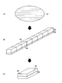
図8(a)に示すように、ナトリウムをフラックスとして液相成長により作製したGaN基板上にエピ成長させ、レーザ構造を加工し、電極を形成した半導体レーザのウェハー81を作製する。これを、図8(b)に示すように、バーに加工する。バーの発光面は、レーザ共振器の反射率を制御、および端面保護、さらにはナトリウムの拡散を防止するため、コーティングを形成する。このコーティング膜には、少なくとも窒化シリコン層が含まれていて、ナトリウムの拡散を防止する。なお、同図において、LPE−GaN基板82上に、デバイス構造83を形成し、さらに電極84を形成してもよい。次に、図8(c)に示すように、発光部の端面をコーティングしたバーをチップ化する。分割したチップ側面(分割面)85には、部分的に転位や欠陥によるナトリウム不純物領域(図示せず)が現れるおそれがあるため、ナトリウムの拡散を防止するためには、分割面にも窒化シリコンなどの薄膜層を形成することが必要となる。これにより、ナトリウムの拡散によるリーク電流が大幅に低減でき、安定なデバイス動作を実現できる。なお、同図において86は発光面を示す。
As shown in FIG. 8A, a
ここでは、薄膜層として窒化シリコンを使用したが、窒化アルミニウム、炭化シリコン、ダイヤモンドライクカーボンなども、ナトリウムに対するバリア性が高く、効果的に利用できる。 Here, silicon nitride is used as the thin film layer, but aluminum nitride, silicon carbide, diamond-like carbon, and the like have high barrier properties against sodium and can be effectively used.
本発明は、例えば、レーザダイオード、発光ダイオード、電界効果トランジスタ等の様々な半導体装置に適用可能である。 The present invention can be applied to various semiconductor devices such as a laser diode, a light emitting diode, and a field effect transistor.
11 21 41 51 71 601 支持基板
12 22 42 72 602 シード層
13a 23a 43a LPE−GaN
13 23 43 73 603 III族元素窒化物結晶基板
14 24 44 74 604 貫通転位
15 25 45 605 薄膜層
16 26 46 606 GaN層
17 27 47 AlGaN層
18 III族元素窒化物結晶層
48 ソース電極
49 ショットキーゲート電極
50 ドレイン電極
500 半導体レーザ
52 58 コンタクト層
53 57 クラッド層
54 56 光ガイド層
55 609 活性層
59 612 絶縁膜
60 611 p型電極
61 614 n型電極
81 ウェハー
82 LPE−GaN基板
83 デバイス構造
84 電極
85 分割面
86 発光面
300 揺動型LPE装置
301 育成炉
302 ヒータ
303 熱電対
304 坩堝固定台
305 回転軸
306 坩堝
307 融解液
308 種結晶
309 流量調節器
310 原料ガス
607 n−GaN層
608 nクラッド層
610 リッジ部
613 pクラッド層
615 選択成長膜
616 対称軸
11 21 41 51 71 601
13 23 43 73 603 Group III element
Claims (19)
前記基板が、アルカリ金属およびアルカリ土類金属の少なくとも一方を含む融解液(フラックス)中において、窒素含有ガスの窒素とIII族元素とを反応させて結晶化させることにより製造されたものであり、
前記基板上であって、前記デバイス構造と前記基板との間に薄膜層が形成されており、
前記薄膜層における前記基板中の不純物の拡散係数が、前記基板における前記基板中の不純物の拡散係数よりも小さいことを特徴とする半導体デバイス。 A group III element nitride semiconductor device in which a group III element nitride crystal layer forming a device structure is laminated on a group III element nitride crystal substrate,
In the melt (flux) containing at least one of an alkali metal and an alkaline earth metal, the substrate is produced by reacting nitrogen of a nitrogen-containing gas with a group III element to crystallize,
On the substrate , a thin film layer is formed between the device structure and the substrate ,
A semiconductor device, wherein a diffusion coefficient of impurities in the substrate in the thin film layer is smaller than a diffusion coefficient of impurities in the substrate in the substrate.
Priority Applications (1)
| Application Number | Priority Date | Filing Date | Title |
|---|---|---|---|
| JP2004299311A JP4824920B2 (en) | 2003-10-20 | 2004-10-13 | Group III element nitride crystal semiconductor device |
Applications Claiming Priority (5)
| Application Number | Priority Date | Filing Date | Title |
|---|---|---|---|
| JP2003359709 | 2003-10-20 | ||
| JP2003359709 | 2003-10-20 | ||
| JP2004188478 | 2004-06-25 | ||
| JP2004188478 | 2004-06-25 | ||
| JP2004299311A JP4824920B2 (en) | 2003-10-20 | 2004-10-13 | Group III element nitride crystal semiconductor device |
Publications (3)
| Publication Number | Publication Date |
|---|---|
| JP2006041458A JP2006041458A (en) | 2006-02-09 |
| JP2006041458A5 JP2006041458A5 (en) | 2007-11-15 |
| JP4824920B2 true JP4824920B2 (en) | 2011-11-30 |
Family
ID=35906086
Family Applications (1)
| Application Number | Title | Priority Date | Filing Date |
|---|---|---|---|
| JP2004299311A Expired - Fee Related JP4824920B2 (en) | 2003-10-20 | 2004-10-13 | Group III element nitride crystal semiconductor device |
Country Status (1)
| Country | Link |
|---|---|
| JP (1) | JP4824920B2 (en) |
Families Citing this family (9)
| Publication number | Priority date | Publication date | Assignee | Title |
|---|---|---|---|---|
| JP4932305B2 (en) * | 2006-03-30 | 2012-05-16 | 株式会社豊田中央研究所 | Method for producing group III nitride compound semiconductor device |
| JP2007277055A (en) * | 2006-04-07 | 2007-10-25 | Toyoda Gosei Co Ltd | Method for manufacturing semiconductor crystal and semiconductor substrate |
| JP4915563B2 (en) * | 2006-09-13 | 2012-04-11 | パナソニック株式会社 | Method of growing gallium nitride single crystal and gallium nitride single crystal obtained thereby |
| US7708833B2 (en) | 2007-03-13 | 2010-05-04 | Toyoda Gosei Co., Ltd. | Crystal growing apparatus |
| JP4926996B2 (en) * | 2007-03-13 | 2012-05-09 | 豊田合成株式会社 | Crystal growth equipment |
| JP2009029672A (en) * | 2007-07-27 | 2009-02-12 | Sumitomo Electric Ind Ltd | Group iii nitride crystal and method for growing the same |
| US7892513B2 (en) * | 2009-01-26 | 2011-02-22 | Sumitomo Electric Industries, Ltd. | Group III nitride crystal and method of its growth |
| JP5564842B2 (en) | 2009-07-10 | 2014-08-06 | サンケン電気株式会社 | Semiconductor device |
| JP5903818B2 (en) * | 2011-09-26 | 2016-04-13 | 富士通株式会社 | Compound semiconductor device and manufacturing method thereof |
Family Cites Families (6)
| Publication number | Priority date | Publication date | Assignee | Title |
|---|---|---|---|---|
| JPS593920A (en) * | 1982-06-29 | 1984-01-10 | Fujitsu Ltd | Manufacture of semiconductor device |
| JP3771333B2 (en) * | 1996-10-30 | 2006-04-26 | 日本オプネクスト株式会社 | Semiconductor laser device and manufacturing method thereof |
| JP3139445B2 (en) * | 1997-03-13 | 2001-02-26 | 日本電気株式会社 | GaN-based semiconductor growth method and GaN-based semiconductor film |
| JP2001148543A (en) * | 1999-11-19 | 2001-05-29 | Sony Corp | Method of manufacturing iii nitride semiconductor, and method of manufacturing semiconductor device |
| JP4749583B2 (en) * | 2001-03-30 | 2011-08-17 | 豊田合成株式会社 | Manufacturing method of semiconductor substrate |
| JP4048476B2 (en) * | 2001-05-22 | 2008-02-20 | 株式会社リコー | III-nitride crystal manufacturing apparatus with observation function and nitride crystal manufacturing method |
-
2004
- 2004-10-13 JP JP2004299311A patent/JP4824920B2/en not_active Expired - Fee Related
Also Published As
| Publication number | Publication date |
|---|---|
| JP2006041458A (en) | 2006-02-09 |
Similar Documents
| Publication | Publication Date | Title |
|---|---|---|
| US7227172B2 (en) | Group-III-element nitride crystal semiconductor device | |
| JP4588340B2 (en) | Method for manufacturing group III nitride substrate | |
| US7176115B2 (en) | Method of manufacturing Group III nitride substrate and semiconductor device | |
| JP5026271B2 (en) | Method for producing hexagonal nitride single crystal, method for producing hexagonal nitride semiconductor crystal and hexagonal nitride single crystal wafer | |
| JP4422473B2 (en) | Method for manufacturing group III nitride substrate | |
| US7221037B2 (en) | Method of manufacturing group III nitride substrate and semiconductor device | |
| US7524691B2 (en) | Method of manufacturing group III nitride substrate | |
| US7125801B2 (en) | Method of manufacturing Group III nitride crystal substrate, etchant used in the method, Group III nitride crystal substrate, and semiconductor device including the same | |
| US8231726B2 (en) | Semiconductor light emitting element, group III nitride semiconductor substrate and method for manufacturing such group III nitride semiconductor substrate | |
| US7309534B2 (en) | Group III nitride crystals usable as group III nitride substrate, method of manufacturing the same, and semiconductor device including the same | |
| JP4397695B2 (en) | Method for manufacturing group III nitride substrate | |
| JP4597534B2 (en) | Method for manufacturing group III nitride substrate | |
| JP2004224600A (en) | Manufacturing method of group iii nitride substrate, and semiconductor device | |
| US7255742B2 (en) | Method of manufacturing Group III nitride crystals, method of manufacturing semiconductor substrate, Group III nitride crystals, semiconductor substrate, and electronic device | |
| JP4486435B2 (en) | Group III nitride crystal substrate manufacturing method and etching solution used therefor | |
| JP3940673B2 (en) | Method for producing group III nitride semiconductor crystal and method for producing gallium nitride compound semiconductor | |
| JP2006008416A (en) | Group iii nitride crystal usable as group iii nitride substrate, method of manufacturing the same, and semiconductor device using the same | |
| JP4824920B2 (en) | Group III element nitride crystal semiconductor device | |
| JP2004300024A (en) | Method for manufacturing nitride crystal of group iii element, nitride crystal of group iii element obtained by the same, and semiconductor device obtained by using the same | |
| JP4554287B2 (en) | Group III nitride crystal manufacturing method and semiconductor substrate manufacturing method | |
| JP2005119893A (en) | Inorganic composition, its production method, and method for producing nitride of group iii element using the same | |
| JP4451265B2 (en) | Group III element nitride crystal substrate and group III element nitride semiconductor device manufacturing method | |
| JP2005251961A (en) | Group iii nitride single crystal wafer and method for manufacturing semiconductor device using same | |
| JPH05190900A (en) | Manufacture of semiconductor light-emitting device | |
| JP2003218468A (en) | Semiconductor laser element and manufacturing method therefor |
Legal Events
| Date | Code | Title | Description |
|---|---|---|---|
| A521 | Written amendment |
Free format text: JAPANESE INTERMEDIATE CODE: A523 Effective date: 20071001 |
|
| A621 | Written request for application examination |
Free format text: JAPANESE INTERMEDIATE CODE: A621 Effective date: 20071001 |
|
| A977 | Report on retrieval |
Free format text: JAPANESE INTERMEDIATE CODE: A971007 Effective date: 20110530 |
|
| A131 | Notification of reasons for refusal |
Free format text: JAPANESE INTERMEDIATE CODE: A131 Effective date: 20110607 |
|
| A521 | Written amendment |
Free format text: JAPANESE INTERMEDIATE CODE: A523 Effective date: 20110728 |
|
| TRDD | Decision of grant or rejection written | ||
| A01 | Written decision to grant a patent or to grant a registration (utility model) |
Free format text: JAPANESE INTERMEDIATE CODE: A01 Effective date: 20110818 |
|
| A01 | Written decision to grant a patent or to grant a registration (utility model) |
Free format text: JAPANESE INTERMEDIATE CODE: A01 |
|
| A61 | First payment of annual fees (during grant procedure) |
Free format text: JAPANESE INTERMEDIATE CODE: A61 Effective date: 20110909 |
|
| R150 | Certificate of patent or registration of utility model |
Free format text: JAPANESE INTERMEDIATE CODE: R150 |
|
| FPAY | Renewal fee payment (event date is renewal date of database) |
Free format text: PAYMENT UNTIL: 20140916 Year of fee payment: 3 |
|
| LAPS | Cancellation because of no payment of annual fees |