JP4801242B2 - Method for manufacturing semiconductor device - Google Patents
Method for manufacturing semiconductor device Download PDFInfo
- Publication number
- JP4801242B2 JP4801242B2 JP2000232507A JP2000232507A JP4801242B2 JP 4801242 B2 JP4801242 B2 JP 4801242B2 JP 2000232507 A JP2000232507 A JP 2000232507A JP 2000232507 A JP2000232507 A JP 2000232507A JP 4801242 B2 JP4801242 B2 JP 4801242B2
- Authority
- JP
- Japan
- Prior art keywords
- semiconductor layer
- island
- shaped semiconductor
- region
- tft
- Prior art date
- Legal status (The legal status is an assumption and is not a legal conclusion. Google has not performed a legal analysis and makes no representation as to the accuracy of the status listed.)
- Expired - Fee Related
Links
Images


Landscapes
- Devices For Indicating Variable Information By Combining Individual Elements (AREA)
- Liquid Crystal (AREA)
- Internal Circuitry In Semiconductor Integrated Circuit Devices (AREA)
- Metal-Oxide And Bipolar Metal-Oxide Semiconductor Integrated Circuits (AREA)
- Thin Film Transistor (AREA)
Description
【0001】
【発明の属する技術分野】
本発明は絶縁表面を有する基板上に薄膜トランジスタ(以下、薄膜トランジスタをTFTと記す)で構成された回路を有する半導体装置およびその作製方法に関する。特に本発明は、画素部とその周辺に設けられる駆動回路を同一の基板上に設けた液晶表示装置に代表される電気光学装置、および電気光学装置を搭載した電子機器に好適に利用できる技術を提供する。尚、本明細書において半導体装置とは、半導体特性を利用することで機能する装置全般を指し、上記電気光学装置およびその電気光学装置を搭載した電子機器をその範疇に含んでいる。
【0002】
【従来の技術】
アクティブマトリクス型の液晶表示装置に代表される電気光学装置のTFTの積層構造の例として、トップゲート型を成す場合、(1)半導体層、(2)ゲート絶縁層、(3)ゲート電極、(4)層間絶縁層、(5)ソース配線、の5層が挙げられる。そして前記TFTを形成するにあたり、(1)半導体層の分離、(2)ゲート絶縁層形成、(3)ゲート電極形成、(4)配線と、ゲート電極及びソース電極を接続する箇所にあたる層間絶縁層に開口部を形成、(5)ソース配線形成、の計5種類のマスクを用いることが挙げられる。前記計5種類のマスクを用いるということは、5回のフォトリソグラフィーの工程が行われることを意味する。
【0003】
また、前記TFTにおける活性層すなわち半導体層は、ガラスなどの基板上に気相成長法などにより形成される。近年この活性層の半導体層を結晶化させる技術が進み、結晶構造を含む半導体(以下、結晶質半導体と記す)層(代表的には、結晶質シリコン或いは多結晶シリコン)を活性層としたTFTでは、高い電界効果移動度が得られることからnチャネル型TFTとpチャネル型TFTとから成るCMOS回路を機能させることができた。CMOS回路を形成することが可能になれば、画素部の他に駆動回路を同一基板上に一体形成でき、液晶表示装置において軽量化および薄型化が可能になるなど、利用範囲は大きい。しかしながら、nチャネル型のみもしくはpチャネル型のみのTFT構造に比べ、構造は複雑になり、工程数は多くなる。
【0004】
【発明が解決しようとする課題】
上に示したように、前記TFTの作製工程は多い。結晶質半導体層を活性層に適用し、画素部に設けたTFTの他に駆動回路を作製する場合は特に多くなる。
【0005】
TFTの作製工程の多さの目安の一つに、工程に用いるフォトマスクの枚数が挙げられる。フォトマスクはフォトリソグラフィーの技術において、エッチング工程のマスクとするレジストパターンを基板上に形成するために用いる。従って、フォトマスクを1枚使用することは、その前後の工程において、被膜の成膜およびエッチングなどの工程の他に、レジスト剥離、洗浄や乾燥工程などが付加され、フォトリソグラフィーの工程においても、レジスト塗布、プレベーク、露光、現像、ポストベークなどの煩雑な工程が行われることを意味する。工程数の増加は製造コストの増加要因になるばかりか、製造歩留まりを低下させる原因となることは明らかである。
【0006】
本発明はこのような問題点を解決する手段を提供することを目的とする。すなわち工程数を削減し、特に工程に用いるフォトマスクを削減することで、レジスト塗布、プレベーク、露光、現像、及びその前後における洗浄や乾燥工程等も省略し、全体として大幅な工程削減をすることを目的とする。
【0007】
【課題を解決するための手段】
本発明では、TFTの製造に要するフォトマスクの枚数を削減し、製造工程の数を削減する技術を提供する。
【0008】
上記課題を解決するため、本発明では、トップゲート型TFTの積層構造を簡素にし、3層構造とした。
すなわち本発明では、基板の上に、半導体層と、前記半導体層上の絶縁層と、前記絶縁層上の導電層が形成される。
【0009】
前記3層構造でTFTを形成するために、ソース配線と、ゲート配線を同一の導電層で形成する。
【0010】
保持容量は、1019atomic/cm3以上の不純物が添加された半導体層と、半導体層上の絶縁層と、絶縁層上の導電層より形成する。
【0011】
またゲート配線については、島状導電層と、1019atomic/cm3以上の一導伝型不純物が添加され前記島状導電層に接続した島状半導体層と、から形成する。そしてソース配線と交差させる部分は島状半導体層で形成され、絶縁層を介して交差させる。但し抵抗が大きくなることが予想されるため、前記島状半導体層の大きさを適当なものとする。さらに保持容量配線の形成手段として、ゲート配線に接続し、前記島状半導体層の交差する長さを小さくする方法を挙げる。この詳細は発明の実施の形態に示す。
【0012】
この手段によれば、ゲート配線とソース配線が交差する、TFTを有する半導体装置が3層構造で作製される。
【0013】
また製造工程において、フォトマスクは、(1)島状半導体層の形成、(2)一導伝型の不純物領域の形成、(3)絶縁層の形成、(4)導電層の形成、のために用い、すなわち計4枚使用する。
【0014】
このような手段を用い、本発明の構成は、基板上にTFTを設けた半導体装置において、第一の絶縁表面上に、チャネル領域と、ソース領域と、ドレイン領域と、前記チャネル領域と前記ソース領域の間の領域と、前記チャネル領域と前記ドレイン領域の間の領域と、保持容量を形成する領域と、を形成する第一の島状半導体層と、前記第一の絶縁表面上に第二の島状半導体層と、前記第一の絶縁表面の上方に形成された第二の絶縁表面上に、前記チャネル領域と交差し、かつ前記第二の島状半導体層と電気的に接続している第一の配線と、前記第二の絶縁表面上に前記保持容量を形成する領域と重なり、かつ前記第二の島状半導体層と交差する第二の配線と、を有し、前記ソース領域、前記ドレイン領域、前記保持容量を形成する領域、及び前記第二の島状半導体層は、1019atomic/cm3以上の濃度の一導伝型の不純物が添加されていることを特徴とする。
【0015】
また他の発明の構成は、基板上にTFTを設けた半導体装置において、第一の絶縁表面上に、チャネル領域と、ソース領域と、ドレイン領域と、前記チャネル領域と前記ソース領域の間の領域と、前記チャネル領域と前記ドレイン領域の間の領域と、保持容量を形成する領域と、を形成する第一の島状半導体層と、前記第一の絶縁表面上に第二の島状半導体層と、前記第一の絶縁表面の上方に形成された第二の絶縁表面上に、前記チャネル領域と交差し、かつ前記第二の島状半導体層と電気的に接続している第一の配線と、前記第二の絶縁表面上に前記保持容量を形成する領域と重なり、かつ前記第一の配線と隣り合う第一の配線と電気的に接続している第二の配線と、を有し、前記ソース領域、前記ドレイン領域、前記保持容量を形成する領域、及び前記第二の島状半導体層は、1019atomic/cm3以上の濃度の一導伝型の不純物が添加されていることを特徴とする。
【0016】
本発明の半導体装置の作製方法に関する構成は、基板上にpチャネル型TFTとnチャネル型TFTとを有する半導体装置の作製方法において、前記基板上に結晶構造を含む半導体層を形成する第1の工程と、前記結晶構造を含む半導体層を選択的にエッチングして第1の島状半導体層及び第2の島状半導体層を形成する第2の工程と、前記第1の島状半導体層に、n型を付与する不純物元素を添加して1019atomic/cm3以上の濃度のn型不純物領域を選択的に形成する第3の工程と、前記第1の島状半導体層及び前記第2の島状半導体層の上に絶縁層を形成する第4の工程と、前記絶縁層を選択的にエッチングする第5の工程と、前記第2の島状半導体層に、p型を付与する不純物元素を添加して1019atomic/cm3以上の濃度のp型不純物領域を選択的に形成する第6の工程と、前記絶縁層もしくは前記第1の島状半導体層及び前記第2の島状半導体層の上に導電層を形成する第7の工程と、前記導電層を選択的にエッチングする第8の工程と、前記第1の島状半導体層または前記第2の島状半導体層に、前記絶縁層を通過させて一導伝型の不純物元素を添加し、一導伝型の不純物領域と形成する第9の工程と、前記第1の島状半導体層及び前記第2の島状半導体層に添加された不純物元素を活性化する第10の工程と、を有することを特徴とする。
【0017】
また、他の作製方法に関する構成は、基板上にpチャネル型TFTとnチャネル型TFTとを有する半導体装置の作製方法において、前記基板上に非結晶構造の半導体層を形成する第1の工程と、前記非結晶構造の半導体層にニッケル、鉄、パラジウム、スズ、鉛、コバルト、白金、銅、金のうち何れかを添加する第2の工程と、前記半導体層を熱処理し、結晶構造を含む半導体層を形成する第3の工程と、前記結晶構造を含む半導体層を選択的にエッチングして第1の島状半導体層及び第2の島状半導体層を形成する第4の工程と、前記第1の島状半導体層に、選択的に、リン、もしくはリンとn型を付与する不純物元素、を添加して1019atomic/cm3以上の濃度のn型不純物領域を形成する第5の工程と、前記第1の島状半導体層及び前記第2の島状半導体層の上に絶縁層を形成する第6の工程と、前記絶縁層を選択的にエッチングする第7の工程と、前記第2の島状半導体層に、選択的に、リンと1019atomic/cm3以上の濃度のp型を付与する不純物が添加された領域を形成する第8の工程と、前記第1の島状半導体層及び前記第2の島状半導体層を熱処理もしくはレーザー照射処理する第9の工程と、前記絶縁層もしくは前記第1の島状半導体層及び前記第2の島状半導体層の上に導電層を形成する第10の工程と、前記導電層を選択的にエッチングする第11の工程と、前記第1の島状半導体層及び前記第2の島状半導体層に、前記絶縁層を通過させn型を付与する不純物元素を添加して、n型不純物領域を形成する第12の工程と、前記第1の島状半導体層及び前記第2の島状半導体層に添加された不純物元素を活性化する第13の工程と、を有することを特徴とする。
【0018】
また、他の作製方法に関する構成は、nチャネル型もしくはpチャネル型のTFTを基板上に設けた半導体装置の作製方法において、前記基板上に結晶構造を含む半導体層を形成する第1の工程と、前記結晶構造を含む半導体層を選択的にエッチングして複数の島状半導体層を形成する第2の工程と、前記島状半導体層に、選択的に1019atomic/cm3以上の濃度の前記nチャネル型もしくはpチャネル型の不純物領域を形成する第3の工程と、前記島状半導体層の上に絶縁層を形成する第4の工程と、前記絶縁層を選択的にエッチングする第5の工程と、前記絶縁層もしくは前記島状半導体層の上に導電層を形成する第6の工程と、前記導電層を選択的にエッチングする第7の工程と、前記島状半導体層に、前記絶縁層を通過させ一導伝型の不純物元素を添加し、選択的に前記一導伝型の不純物領域を形成する第8の工程と、前記島状半導体層に添加された不純物元素を活性化する第9の工程と、を有することを特徴とする。
【0019】
また、他の作製方法に関する構成は、nチャネル型もしくはpチャネル型のTFTを基板上に設けた半導体装置の作製方法において、前記基板上に非結晶構造の半導体層を形成する第1の工程と、前記非結晶構造の半導体層にニッケル、鉄、パラジウム、スズ、鉛、コバルト、白金、銅、金のうち何れかを添加する第2の工程と、前記半導体層を熱処理し、結晶構造を含む半導体層を形成する第3の工程と、前記結晶構造を含む半導体層を選択的にエッチングして複数の島状半導体層を形成する第4の工程と、前記島状半導体層に、選択的に、リン、もしくはリンと1019atomic/cm3以上の濃度の一導伝型の不純物領域を形成する第5の工程と、前記島状半導体層の上に絶縁層を形成する第6の工程と、前記絶縁層を選択的にエッチングする第7の工程と、前記島状半導体層を熱処理もしくはレーザー照射処理する第8の工程と、前記絶縁層もしくは前記島状半導体層の上に導電層を形成する第9の工程と、前記導電層を選択的にエッチングする第10の工程と、前記島状半導体層に、前記絶縁層を通過させ前記一導伝型の不純物領域を形成する第11の工程と、前記島状半導体層に添加された不純物元素を活性化する第12の工程と、を有することを特徴とする。
【0020】
また、他の作製方法に関する構成は、基板上にpチャネル型TFTとnチャネル型TFTとを有する半導体装置の作製方法において、前記基板上に結晶構造を含む半導体層を形成する第1の工程と、前記結晶構造を含む半導体層を選択的にエッチングして前記第1の島状半導体層及び前記第2の島状半導体層を形成する第2の工程と、前記第1の島状半導体層に、選択的に、n型を付与する不純物元素を添加して1019atomic/cm3以上の濃度のn型不純物領域を形成する第3の工程と、前記第1の島状半導体層及び前記第2の島状半導体層の上に絶縁層を形成する第4の工程と、前記絶縁層を選択的にエッチングする第5の工程と、前記第2の島状半導体層に、選択的に、1019atomic/cm3以上の濃度のp型不純物領域を形成する第6の工程と、前記第1の島状半導体層及び前記第2の島状半導体層に添加された不純物元素を活性化する第7の工程と、前記絶縁層もしくは前記第1の島状半導体層及び前記第2の島状半導体層の上に導電層を形成する第8の工程と、前記導電層を選択的にエッチングする第9の工程と、を有することを特徴とする。
【0021】
また、他の作製方法に関する構成は、基板上にpチャネル型TFTとnチャネル型TFTとを有する半導体装置の作製方法において、前記基板上に非結晶構造の半導体層を形成する第1の工程と、前記非結晶構造の半導体層にニッケル、鉄、パラジウム、スズ、鉛、コバルト、白金、銅、金のうち何れかを添加する第2の工程と、前記半導体層を熱処理し、結晶構造を含む半導体層を形成する第3の工程と、前記結晶構造を含む半導体層を選択的にエッチングして前記第1の島状半導体層及び前記第2の島状半導体層を形成する第4の工程と、前記第1の島状半導体層に、選択的に、リン、もしくはリンとn型を付与する不純物元素、を添加して1019atomic/cm3以上の濃度のn型不純物領域を形成する第5の工程と、前記第1の島状半導体層及び前記第2の島状半導体層の上に絶縁層を形成する第6の工程と、前記絶縁層を選択的にエッチングする第7の工程と、前記第2の島状半導体層に、選択的に、リンと1019atomic/cm3以上の濃度のp型不純物が添加された領域を形成する第8の工程と、前記第1の島状半導体層及び前記第2の島状半導体層に添加された不純物元素を活性化する第9の工程と、前記絶縁層もしくは前記第1の島状半導体層及び前記第2の島状半導体層の上に導電層を形成する第10の工程と、前記導電層を選択的にエッチングする第11の工程と、を有することを特徴とする。
【0022】
また、他の作製方法に関する構成は、nチャネル型もしくはpチャネル型のTFTを基板上に設けた半導体装置の作製方法において、前記基板上に結晶構造を含む半導体層を形成する第1の工程と、前記結晶構造を含む半導体層を選択的にエッチングして複数の島状半導体層を形成する第2の工程と、前記島状半導体層に、選択的に1019atomic/cm3以上の濃度の一導伝型の不純物領域を形成する第3の工程と、前記島状半導体層に添加された不純物元素を活性化する第4の工程と、前記島状半導体層の上に絶縁層を形成する第5の工程と、前記絶縁層を選択的にエッチングする第6の工程と、前記絶縁層もしくは前記島状半導体層の上に導電層を形成する第7の工程と、前記導電層を選択的にエッチングする第8の工程と、を有することを特徴とする。
【0023】
また、他の作製方法に関する構成は、nチャネル型もしくはpチャネル型のTFTを基板上に設けた半導体装置の作製方法において、前記基板上に非結晶構造の半導体層を形成する第1の工程と、前記非結晶構造の半導体層にニッケル、鉄、パラジウム、スズ、鉛、コバルト、白金、銅、金のうち何れかを添加する第2の工程と、前記半導体層を熱処理し、結晶構造を含む半導体層を形成する第3の工程と、前記結晶構造を含む半導体層を選択的にエッチングして複数の島状半導体層を形成する第4の工程と、前記島状半導体層に、選択的に、リン、もしくはリンと1019atomic/cm3以上の濃度の一導伝型の不純物領域を形成する第5の工程と、前記島状半導体層に添加された不純物元素を活性化する第6の工程と、前記島状半導体層の上に絶縁層を形成する第7の工程と、前記絶縁層を選択的にエッチングする第8の工程と、前記絶縁層もしくは前記島状半導体層の上に導電層を形成する第9の工程と、前記導電層を選択的にエッチングする第10の工程と、を有することを特徴とする。
【0024】
【発明の実施の形態】
本発明の実施の形態について、図1〜図8を用いて説明する。
【0025】
本発明によって作製されるトップゲート型TFTの、構成の一例を図1に上面図として示す。図1はこの発明が適用された、アクティブマトリクス型LCDとして線幅が充分大きく画素数が充分小さい構成であり、ゲート配線の抵抗を考慮せずに済むときの例を示している。また、反射型液晶表示装置に用いられる構成としている。
【0026】
図1(a)は、画素部の構成を表す上面図である。TFTを構成する半導体1007のソース領域は、一方向に伸びた形で形成される導電性配線1002に接続している。またドレイン領域には、反射電極用の導電層1004が接続するとともに、半導体からなる領域1003が延在している。該半導体からなる領域1003は、絶縁成膜を介して導電層1011と重なり、保持容量として機能する。
【0027】
ドレイン領域から延在した保持容量を形成する半導体からなる領域1003に、絶縁性層を介して重なるように、保持容量を形成する導電層領域1011が形成されている。前記保持容量を形成する導電層からなる領域1011は、前記導電性配線1002と重ならないよう形成される、保持容量用導電性配線1006に接続している。
【0028】
また、TFTを構成するゲート電極及びゲート配線は、導電層1001により形成される。前記導電層1001は、半導体からなる導電部分1005に接続している。前記半導体からなる導電部分1005は、前記一方向に伸びた形で形成される導電性配線1002及び前記保持容量用導電性配線1006と、絶縁層を介して交わっている。
【0029】
図1(b)は、駆動回路におけるn型TFTの構成を表す上面図である。ゲート電極には導電性配線1009が延在し、ソース、ドレイン領域に重なるゲート絶縁層には開口部が設けられ、導電性配線1008と接続している。
【0030】
また、図1(c)は、駆動回路におけるp型TFTの構成を表す上面図である。ゲート電極には導電性配線1010が延在している。前記導電性配線1010が前記p型TFTの半導体層1013と重なる部分以外はゲート絶縁層に開口部が設けられ、ソース、ドレイン領域には導電性配線1012が接続している。
【0031】
図2(a)、図2(b)、図2(c)、はそれぞれ、図1中に破線A1〜A2、破線B1〜B2、破線C1〜C2、で示された部分の断面図を示す。破線A1〜A2で示された部分は駆動回路部分であり、説明の都合上、n型TFT及びp型TFTを並べている。
【0032】
図2(a)で示された駆動回路のn型TFT2001は、半導体層において、ソースもしくはドレイン部分2005と、チャネル部分2006を有する。また前記ソースもしくはドレイン部分2005と、チャネル部分2006の間には、オフセット領域もしくはLDD領域2007が形成される。前記オフセット領域もしくはLDD領域2007は、オフリーク電流を小さくするため有効である。
【0033】
図2(a)で示された駆動回路のp型TFT2002は、半導体層において、ソースもしくはドレイン部分2008と、チャネル部分2009を有する。また前記ソースもしくはドレイン部分2008と、チャネル部分2009の間には、オフセット領域もしくはLDD領域2010が形成される。前記オフセット領域もしくはLDD領域2010は、オフリーク電流を小さくするため有効である。
【0034】
図2(b)で示された画素部のTFT2003は、半導体層において、ソースもしくはドレイン部分2011と、チャネル部分2012を有する。また前記ソースもしくはドレイン部分2011と、チャネル部分2012の間には、オフセット領域もしくはLDD領域2013が形成される。前記オフセット領域もしくはLDD領域2013は、オフリーク電流を小さくするため有効である。
【0035】
以上のオフセット領域もしくはLDD領域の形状は、必要な特性に応じて設計する。例えば駆動回路のP型TFTにおいては、ソースもしくはドレイン部分と、チャネル部分の間隔は2μm以下が適当であり、これ以上の長さではオン電流が小さくなってしまう。
【0036】
図2(C)で示されたゲート電極及びゲート配線2004は、導電性配線2015と、n型を付与する高濃度の不純物を有する半導体層2014からなる。
【0037】
但し、図1で示した構成では、配線の線幅が大きく、ゲート配線の抵抗が充分小さい場合のみ適用できる。微細化された構成においては、配置に工夫が必要となる。
【0038】
図3(A)で示される様に、ゲート配線は導電性配線3001と、n型を付与する高濃度の不純物を有する半導体層3002とのチェーン状になる。ここで問題は、n型を付与する高濃度の不純物を有する半導体層3002の抵抗率が高いことにある。
【0039】
我々の作成した1021atoms/cm3程度リンが添加されたシリコン層の抵抗率は、加工後には2×103Ωcm前後となる。抵抗率が前記2×103Ωcm前後の半導体層は、導電性配線として汎用されるAlの抵抗率4μΩcm前後であるのに比べ、3桁程度大きい。また、Alの導電性配線は400nmで形成されることに対し、半導体層は結晶化等の理由からこれより小さい膜厚で形成されることが多い。
【0040】
すなわち導電性材料のみで形成された従来のゲート配線より抵抗は大きくなることが予想され、特に前記高濃度の不純物を有する半導体層の線幅を検討する必要がある。例えば、画素ピッチが42×126μmである直視型LCDにおいて、導電性配線の抵抗及びコンタクト抵抗を0とし、半導体層の厚さを50nmと仮定した場合、駆動するために必要な、n型を付与する高濃度の不純物を有する半導体層3002の線幅は最低50μmと見積もられる。この様に前記半導体層3002の線幅が広い場合には、図3(B)に示すように、前記半導体層3002は、ゲート絶縁層を介してソース配線と並列するように配置することになる。
【0041】
さらに、前記半導体層3002に重なるよう形成された保持容量配線3005,3006,3007は、図3(B)に示すように、隣のゲート配線3004より延在させ接続することで、前記半導体層3002の上に形成しなくて済む。このとき、隣のゲート配線3004が保持容量配線を兼ねることになる。このとき、前記半導体層3002の長さを短くすることが出来る。図4(A)は図2及び図3におけるゲート配線を示す断面図である。図4(A)すなわち図2の配置の様に配線間隔4001,4002,4003を2μm、配線4002,4004の間隔を5μmとし、コンタクト開口部までの長さ4006,4007を4μmとした場合、一つの高濃度の不純物を有する半導体層の長さは24μmと算出できる。これに対し、図3のごとく前記隣のゲート配線が保持容量配線を兼ねる方法を用いれば、図4(A)の部分は図4(B)のごとく形成され、各間隔4008,4009,4010,4011,4012の合計は17μmとなり、抵抗を約2/3に小さくすることが出来る。
【0042】
すなわち、画素付近の回路を図3(B)のごとく形成すれば、抵抗を小さくすることができる。
【0043】
多結晶シリコン層にリンを加えたときの導電率特性を図23(M. M. Mandurah, J.Electrochem.Soc. 126.1019-1023 (June.1979) )に示す。図中poly-crystalline シリコンの曲線で示されるように、リン濃度が1019atoms/cm3前後で抵抗率の変化が異なる。1019atoms/cm3より小さくなるにつれ、粒界にキャリアがトラップされ、結晶中のキャリアが少なくなり抵抗が高くなる。1019atoms/cm3からリン濃度が大きくなると抵抗率は小さくなるが、その依存性は前記1019atoms/cm3より小さくなる変化に比べて緩やかになる。
【0044】
我々の作成した、1021atoms/cm3程度リンが添加されたシリコン層の抵抗率は、2×103Ωcm前後となる。これは抵抗率を小さくする目的で、大きな濃度で添加しているが、回路設計により若干の抵抗の増大は許容される。従来のTFTにおいて、ソース及びドレイン領域に添加された1019atoms/cm3以上のものが多いことから、我々は前記多結晶シリコン中にリンに限らず不純物元素が1019atoms/cm3以上添加されていれば、シリコンに導電性を持たせることが可能と考えた。このシリコン中に添加された1019atoms/cm3以上の不純物の濃度を、本明細書では高濃度と記す。
【0045】
以上の構成で動作可能な、液晶表示装置について評価する。半導体層を結晶化した場合、CMOS回路を作製することが可能となる。このとき全ての素子にオフセット領域またはLDD領域を設けることで、オフリーク電流を小さくすることができる。しかしながらP型TFTからなる駆動回路を形成するとき、オフセット領域またはLDD領域によって、オン電流が小さくなることが予想される。表1には、幅8μm×8μmのTFTにおいて、前記オフセット領域またはLDD領域を形成したときの、ON電流値を示す。
【0046】
【表1】

シフトレジスタは一方向の画素数分のトランジスタが連結されている。前記一方向の画素数が一定の場合、シフトレジスタを小さいON電流値で、かつ高い周波数で駆動すると、TFTにおいて充電もしくは放電がしきれず、信号が流れなくなる。したがって、ON電流値により周波数は制限される。また、画素部において、ゲート配線はメタル部分と半導体部分が直列でつながっており、この抵抗増加に起因した信号の遅延がおきる。信号の遅延が起きた場合、ゲート電極に印加する信号の有効時間が短くなるため、ビデオ信号の分割を行うなどで解決する。
【0048】
前記シフトレジスタの動作限界を考慮し、シミュレーションにより、必要なオン電流を流すための前記オフセット領域またはLDD領域中の不純物量と、前記オフセット領域またはLDD領域の幅を見積もった。本発明においては、画素数640×3(RGB)×480、画素ピッチ42μm×126μmであり、周辺にp型TFT及びn型TFTからなる駆動回路が設けられ、4分割されたビデオ信号に対応する液晶表示用電気光学装置を例にする。その結果、シフトレジスタに関しては、シミュレーションによれば、シフトレジスタは、駆動する周波数は5MHz以下において動作すると見積もられた。このとき前記LDD領域の不純物がn型を付与する不純物の場合、前記LDD領域の幅は0.5μm以下で動作し、p型を付与する不純物の場合、前記LDD領域の幅は1μm以下と見積もられた。
【0049】
このように、通常量産される、4inch角で5MHz以下の液晶駆動回路は、この発明による設計においても動作する。
【0050】
以下に、本発明のTFTの作製工程を四例示す。工程例1では基板上にnチャネル型TFTとpチャネル型のTFTを形成し、全てのTFTにLDD領域を形成する工程例を、工程例2では基板上にnチャネル型TFTとpチャネル型のTFTを形成し、全てのTFTにオフセット領域を形成する工程例を、工程例3では基板上にnチャネル型TFTもしくはpチャネル型のTFTを形成し、全てのTFTにLDD領域を形成する工程例を、工程例4では基板上にnチャネル型TFTもしくはpチャネル型のTFTを形成し、全てのTFTにオフセット領域を形成する工程例を、それぞれ示す。いずれの工程例においても、TFTは4枚のフォトマスクを使用することで、作製される。
【0051】
(工程例1)
本発明のTFTの作製工程を表2に示す。表2では、金属不純物を用いて半導体層を結晶化し、基板上に形成される全てのTFTにLDD領域を形成する工程例を示す。該工程を、保持容量配線が、絶縁層を介してゲート電極の高濃度n型不純物が添加された半導体層からなる部分と交差する図1のTFT構成を例にとり説明する。該工程順序及び条件は、保持容量配線が当該保持容量配線と接続したTFTのゲート配線のある方向とは反対側のゲート配線と接続する図3(B)で示される構成の場合にも適用できる。なお表2中では、フォトマスクを使用する工程に*をつけている。
【0052】
【表2】
以下表2の工程に従い、図5〜図8を用いて説明する。図5〜図8は、工程が進むにつれ形成される各層の形状を示す上面図である。
【0054】
基板はガラスもしくは石英から成るものを使用する。ガラスの場合には表面よりアルカリ金属などの拡散を防ぐため、シリコン酸化膜等の下地膜を形成することが望ましい。
【0055】
まず、工程1で示される様に、前記基板上に非結晶質の半導体層を成膜する。シリコンを例にするなら、プラズマCVDもしくは減圧CVDもしくはスパッタによる成膜を行う。シリコン以外にも、ガリウム、ヒ素、ゲルマニウムの何れかを組成としてもつ材料を用いても良い。
【0056】
次に、工程2で示される様に前記非結晶質の半導体層の結晶化を行う。これは熱結晶化、もしくはレーザーによる結晶化、もしくはこれを併用する。この発明において半導体層は、金属不純物を触媒として添加し、結晶化を促進する方法を使用出来る。前記金属不純物はニッケルが効果的であり、以後ニッケルを用いた例を挙げる。ニッケルの添加した場合は、後の工程8で熱結晶化を行い、その後P型TFT部のソース、ドレイン部に高濃度不純物をドーピングした後、ゲッタリング熱処理を行う。
【0057】
次に、工程3で示される様に結晶化された半導体層に、フォトレジストを形成し、ドライエッチングにて形成を行う。このとき、図5(a)に示されるように、画素部の駆動スイッチにあたるTFTのチャネル及び低濃度不純物領域部分5000、および前記TFTのソース領域5001、および前記TFTのドレイン領域5002にあたる部分より延在した保持容量部分5003、ゲート配線の一部となる島状の部分5004、図5(b)に示される駆動回路のn型TFT部、図5(c)に示される駆動回路のp型TFT部、が形成される。なお図5〜8中で駆動回路のソース部分とドレイン部分の区別はしていない。
【0058】
次に、工程4で示される様に高濃度n型不純物を添加する領域を形成する。画素部の駆動スイッチにあたるTFTのソース領域5001、およびそのドレイン領域5002、保持容量を形成する部分5003、ゲート配線の一部となる島状の部分5004、図5(b)に示される駆動回路のn型TFTのソース部分及びドレイン部分5005、の部分以外にフォトレジストを形成し、高濃度n型不純物をドーピングする際のマスクとする。
【0059】
そして工程5で示される様に半導体層において前記ドーピングする際のマスクが形成されていない領域に高濃度n型不純物ドープ領域のドーピングを行う。前記n型不純物として典型的にはリン(P)または砒素(As)を用いるが、ニッケルを用いた結晶化を行う場合はリン(P)を用いる。なぜなら前記半導体層に触媒すなわちニッケルを添加し、半導体層を結晶化する場合には、後工程で熱処理によりリンの添加された領域に偏析させる方法で、チャネル部分の半導体層のリンを除去する、すなわちゲッタリングをする方法が一般的にとられているからである。本発明でもこれを利用する。
【0060】
次に工程6で示される様にゲート絶縁層をプラズマCVDもしくはスパッタ、熱酸化等で、酸化膜もしくは窒化膜を形成する。
【0061】
そして工程7で示される様にゲート絶縁層に、フォトレジストを形成し、ドライエッチングにて開口部を設ける。図6は前記開口部の形状を示している。画素部分のソース領域6001及びドレイン領域6002、ゲート配線の半導体層部分の両端6003、駆動回路のn型TFT部分のソース領域及びドレイン領域6004、P型TFTのチャネル領域にフォトレジストが形成されるときの誤差を加味した幅を除いた領域6006に開口部を設ける。
【0062】
すると前記開口部を設けた部分は、半導体層が露出している。この露出した領域に、工程8で示される様に高濃度のp型不純物をドーピングする。半導体層がシリコンであるとき、典型的にはボロンを用いる。図6中では、ボロンがドーピングされた領域が、前記高濃度のn型不純物を示したハッチングとは異なるハッチングで示されている。このとき、画素部分のソース領域6001及びドレイン領域6002、ゲート配線の半導体層部分の両端6003、駆動回路のn型TFT部分のソース領域及びドレイン領域6004に高濃度のp型不純物がドーピングされるので、該領域のp型不純物はn型不純物濃度を超えない濃度でドーピングする。
【0063】
このため前記p型不純物をドーピングする前後何れかに、リンを、前記p型不純物をドーピングする領域に前記p型不純物濃度を超えない濃度で添加する。その後ゲッタリング熱処理を行う。このときニッケルは各TFTのソース及びドレイン領域にゲッタリングされる。
【0064】
そして、工程9で示される様にスパッタ成膜等で、導電性配線を成膜する。これはゲート配線及びソース配線として、半導体層と接触し導電性を確保する必要があるため、熱により半導体層に拡散せず、かつ抵抗率が上昇しない材料が望ましい。また、前記導電性配線は半導体層に接しているため、後工程でエッチングする際の半導体層と前記配線材料とのエッチング選択比が必要となる。半導体層がシリコンの場合、選択比を大きくするためには、配線材料を薬液でエッチングすることが望ましい。以上の条件より、前記導電性配線材料は、前記TiとAlを積層する他に、Mo、Ag-Pd-Cuが挙げられる。
【0065】
その後工程10で示される様に前記導電性配線に、フォトレジストを形成し、図7に示されるような導電性配線の形状を形成する。画素部TFTのソース部分と接続する配線7001、シリコンで形成されたゲート配線の一部をチェーン状に繋ぐよう接続され、画素部TFTのゲート部上に伸びた配線7002、画素部TFTのドレイン部分に接続する画素電極7003、画素部TFTのドレイン領域にあたる部分より伸びたCs(保持容量)部分に重なるよう形成された保持容量配線7004、を形成する。また駆動回路においては、n型TFT部分のソース配線及びドレイン配線及びゲート配線7005、p型TFT部分のソース配線及びドレイン配線及びゲート配線7006、を形成する。
【0066】
このとき画素部TFTの半導体層において、基板平面を上から見た場合、ゲート配線で遮蔽された部分と低濃度のn型不純物領域の間には、斜線で示された間隔8001がある。また駆動回路においてもn型TFT及びP型TFTに同様の間隔がある。ここに、工程11で示される様にゲート絶縁層を通過させ半導体層にドーピングする、いわゆるスルードープ方法を用い、低濃度の一導伝型不純物を添加する。これにより低濃度の一導伝型不純物領域8002,8003,8004を形成する。
【0067】
その後、工程12で示される様に基板をレーザー照射による処理もしくは500℃前後で加熱処理する。これにより半導体中のn型不純物もしくはp型不純物が安定した位置に収まり、決まった不純物準位が形成される。そして、基板を水素雰囲気で加熱処理し、半導体中もしくは半導体とゲート絶縁層間のダングリングボンドを水素で終端する。これにより界面準位を無くし、特性を向上させる。
【0068】
以上の工程で、結晶化された半導体層を用いたトップゲート型TFTが4枚のマスクで完成する。
【0069】
(工程例2)
本発明のTFTの作製工程を表3に示す。工程例2では、基板上に形成される全てのTFTにオフセット領域を形成する工程例を示す。該工程を、保持容量配線が、絶縁層を介してゲート電極の高濃度n型不純物が添加された半導体層からなる部分と交差するTFT構成を例にとり説明する。該工程順序及び条件は、保持容量配線が当該保持容量配線と接続したTFTのゲート配線のある方向とは反対側のゲート配線と接続する構成の場合にも適用できる。
【0070】
【表3】
表3の工程例において、工程1より、工程8までは工程例1と同様の処理を行う。但し工程8においてゲッタリング熱処理を行う。このときニッケルは各TFTのソース及びドレイン領域にゲッタリングされる。その後工程9で示される様に半導体層の活性化を行う。これにより半導体中のn型不純物もしくはp型不純物が安定した位置に収まり、決まった不純物準位が形成される。工程例1と異なり、半導体層の活性化を行う際、配線材料の耐熱性を考慮する必要が無い利点がある。
【0072】
このとき画素部TFTの半導体層において、基板平面を上から見た場合、ゲート配線で遮蔽された部分と低濃度のn型不純物領域の間には、斜線で示された間隔8001がある。また駆動回路においてもn型TFT及びP型TFTに同様の間隔8002,8003,8004がある。工程例1ではここに不純物を添加するが、工程例2ではここに不純物を添加しない。すなわち前記間隔が真性半導体となりオフセット領域となる。
【0073】
そして工程10、工程11、で示される様に導電性配線を形成する。この導電性配線は、水素雰囲気での加熱処理すなわち300℃程度の耐熱性を持ち、低抵抗の材料が望ましい。
【0074】
その後工程12で示される様に基板を水素雰囲気で加熱処理し、半導体中もしくは半導体とゲート絶縁層間のダングリングボンドを水素で終端する。これにより界面準位を無くし、特性を向上させる。水素化しなくても半導体特性として良好である場合、この工程は無くてもよい。
【0075】
以上の工程で、結晶化された半導体層を用いたトップゲート型TFTが4枚のマスクで完成する。
【0076】
(工程例3)
本発明のTFTの作製工程を表4に示す。表4では、金属不純物を用いて半導体層を結晶化し、基板上にnチャネル型TFTもしくはpチャネル型TFTが形成され、前記TFTにLDD領域を形成する工程例を示す。該工程を、保持容量配線が、絶縁層を介してゲート電極の高濃度n型不純物が添加された半導体層からなる部分と交差するTFT構成を例にとり説明する。該工程順序及び条件は、保持容量配線が当該保持容量配線と接続したTFTのゲート配線のある方向とは反対側のゲート配線と接続する構成の場合にも適用できる。
【0077】
【表4】
以下表4の工程に従い、図19〜図22を用いて説明する。図19〜図22は、工程が進むにつれ形成される各層の形状を示す上面図である。
【0079】
表4の工程例において、工程1〜工程2までは工程例1と同様の処理を行う。
そして工程3で示される様に結晶化された半導体層に、フォトレジストを形成し、ドライエッチングにて島状に形成する。このとき、図19(A)に示されるように、画素部の駆動スイッチにあたるTFTのチャネル及び低濃度不純物領域部分1900、および前記TFTのソース領域1901、および前記TFTのドレイン領域1902にあたる部分より延在した保持容量部分1903、ゲート配線の一部となる島状の部分1904、図19(B)に示される駆動回路の前記nチャネル型TFTもしくはpチャネル型TFT部、が形成される。
【0080】
次に、工程4で示される様に高濃度の前記一導伝型不純物を添加する領域を形成する。画素部の駆動スイッチにあたるTFTのソース領域1901、およびそのドレイン領域1902、保持容量を形成する部分1903、ゲート配線の一部となる島状の部分1904、図19(B)に示される駆動回路の前記一導伝型のソース部分及びドレイン部分1905、の部分以外にフォトレジストを形成し、高濃度の前記一導伝型不純物をドーピングする際のマスクとする。
【0081】
そして工程5で示される様に半導体層において前記ドーピングする際のマスクが形成されていない領域に高濃度の前記一導伝型不純物ドープ領域のドーピングを行う。半導体層がシリコンであるとき、前記nチャネル型TFTもしくはpチャネル型のTFTがn型のTFTであれば、典型的にはリン(P)または砒素(As)を用いるが、ニッケルを触媒とし結晶化を行う場合はリン(P)を用いる。また前記半導体層の結晶化において、ニッケル添加を用いて半導体層を結晶化する場合に、前記nチャネル型TFTもしくはpチャネル型のTFTがp型であれば、当不純物以外に、当不純物を越えない濃度でリンを添加する。なぜならリンはニッケルをゲッタリングする際に有効だからである。その後ゲッタリング熱処理を行う。このときニッケルは各TFTのソース及びドレイン領域にゲッタリングされる。
【0082】
その後、工程6で示される様にゲート絶縁層をプラズマCVDもしくはスパッタ、熱酸化等で、酸化膜もしくは窒化膜を形成する。
【0083】
次に工程7で示される様にゲート絶縁層に、フォトレジストを形成し、ドライエッチングにて開口部を設ける。図20は前記開口部の形状を示している。画素部分のソース領域2021及びドレイン領域2022、ゲート配線の半導体層部分の両端2023、駆動回路の前記nチャネル型TFTもしくはpチャネル型TFT部分のソース領域及びドレイン領域2024、に開口部を設ける。
【0084】
そして工程8で示される様に、スパッタ成膜等で、導電性配線を成膜する。これはゲート配線及びソース配線として、半導体層と接触し導電性を確保する必要があるため、熱により半導体層に拡散せず、かつ抵抗率が上昇しない材料が望ましい。また、前記導電性配線は半導体層に接しているため、後工程でエッチングする際の半導体層と前記配線材料とのエッチング選択比が必要となる。半導体層がシリコンの場合、選択比を大きくするためには、配線材料を薬液でエッチングすることが望ましい。以上の条件より、前記導電性配線材料は、前記TiとAlを積層する他に、Mo、Ag-Pd-Cuが挙げられる。
【0085】
その後工程9で示される様に前記導電性配線に、フォトレジストを形成し、図21に示されるような前記導電性配線の形状を形成する。画素部TFTのソース部分と接続する配線2101、シリコンで形成されたゲート配線の一部をチェーン状に繋ぐよう接続され、画素部TFTのゲート部上に伸びた配線2102、画素部TFTのドレイン部分に接続する画素電極2103、画素部TFTのドレイン領域にあたる部分より伸びたCs(保持容量)部分に重なるよう形成された保持容量配線2104、を形成する。また駆動回路においては、前記nチャネル型TFTもしくはpチャネル型TFT部分のソース配線及びドレイン配線及びゲート配線2105、を形成する。
【0086】
このとき画素部TFTの半導体層において、基板平面を上から見た場合、ゲート配線で遮蔽された部分と低濃度の一導伝型の不純物領域の間には、斜線で示された間隔2201がある。また駆動回路においても前記nチャネル型TFTもしくはpチャネル型TFTに同様の間隔2202,2203がある。ここに、工程10で示される様にゲート絶縁層を通過させ半導体層にドーピングする、いわゆるスルードープ方法を用い、低濃度の前記一導伝型不純物を添加する。これにより低濃度の前記一導伝型の不純物領域を形成する。
【0087】
その後工程11で示される様に基板をレーザー照射による処理もしくは加熱処理する。これにより半導体中の前記一導伝型不純物が安定した位置に収まり、決まった不純物準位が形成される。そして、基板を水素雰囲気で加熱処理し、半導体中もしくは半導体とゲート絶縁層間のダングリングボンドを水素で終端する。これにより界面準位を無くし、特性を向上させる。水素化しなくても半導体特性として良好である場合、この工程は無くてもよい。
【0088】
以上の工程で、結晶化された半導体層を用いたトップゲート型TFTが4枚のマスクで完成する。
【0089】
(工程例4)
本発明のTFTの作製工程を表5に示す。表5では、金属不純物を用いて半導体層を結晶化し、基板上にnチャネル型TFTもしくはpチャネル型TFTが形成され、前記TFTにオフセット領域を形成する工程例を示す。該工程を、保持容量配線が、絶縁層を介してゲート電極の高濃度n型不純物が添加された半導体層からなる部分と交差するTFT構成を例にとり説明する。該工程順序及び条件は、保持容量配線が当該保持容量配線と接続したTFTのゲート配線のある方向とは反対側のゲート配線と接続する構成の場合にも適用できる。
【0090】
【表5】
以下表5の工程に従い、図19〜図22を用いて説明する。図19〜図22は、工程が進むにつれ形成される各層の形状を示す上面図である。
【0092】
表5の工程例において、工程1〜工程5までは工程例3と同様の処理を行う。
【0093】
その後、工程6で示される様に基板をレーザー照射による処理もしくは加熱処理する。これにより前記半導体中の不純物が安定した位置に収まり、決まった不純物準位が形成される。
【0094】
次に工程7で示される様にゲート絶縁層をプラズマCVDもしくはスパッタ、熱酸化等で、酸化膜もしくは窒化膜を形成する。
【0095】
そして工程8で示される様にゲート絶縁層に、フォトレジストを形成し、ドライエッチングにて開口部を設ける。図20は前記開口部の形状を示している。画素部分のソース領域2021及びドレイン領域2022、ゲート配線の半導体層部分の両端2023、駆動回路の前記nチャネル型TFTもしくはpチャネル型TFT部分のソース領域及びドレイン領域2024、に開口部を設ける。
【0096】
そして工程9で示される様に、スパッタ成膜等で、導電性配線を成膜する。これはゲート配線及びソース配線として、半導体層と接触し導電性を確保する必要があるため、熱により半導体層に拡散せず、かつ抵抗率が上昇しない材料が望ましい。また、前記導電性配線は半導体層に接しているため、後工程でエッチングする際の半導体層と前記配線材料とのエッチング選択比が必要となる。半導体層がシリコンの場合、選択比を大きくするためには、配線材料を薬液でエッチングすることが望ましい。以上の条件より、前記導電性配線材料は、前記TiとAlを積層する他に、Mo、Ag-Pd-Cuが挙げられる。
【0097】
その後工程10で示される様に前記導電性配線に、フォトレジストを形成し、図21に示されるような導電性配線の形状を形成する。画素部TFTのソース部分と接続する配線2101、シリコンで形成されたゲート配線の一部をチェーン状に繋ぐよう接続され、画素部TFTのゲート部上に伸びた配線2102、画素部TFTのドレイン部分に接続する画素電極2103、画素部TFTのドレイン領域にあたる部分より伸びたCs(保持容量)部分に重なるよう形成された保持容量配線2104、を形成する。また駆動回路においては、前記nチャネル型TFTもしくはpチャネル型TFT部分のソース配線及びドレイン配線及びゲート配線2105、を形成する。
【0098】
このとき画素部TFTの半導体層において、基板平面を上から見た場合、ゲート配線で遮蔽された部分と低濃度の前記一導伝型不純物領域の間には、斜線で示された間隔2201がある。また駆動回路においても前記nチャネル型TFTもしくはpチャネル型TFTに同様の間隔2202,2203がある。ここに、ゲート絶縁層を通過させ半導体層にドーピングする、いわゆるスルードープ方法を用い、低濃度の前記一導伝型不純物を添加する。これにより低濃度の前記一導伝型不純物領域を形成する。
【0099】
そして、基板を水素雰囲気で加熱処理し、半導体中もしくは半導体とゲート絶縁層間のダングリングボンドを水素で終端する。これにより界面準位を無くし、特性を向上させる。水素化しなくても半導体特性として良好である場合、この工程は無くてもよい。
【0100】
以上の工程で、結晶化された半導体層を用いたトップゲート型TFTが4枚のマスクで完成する。
【0101】
また、本発明によれば、画素部に設けたTFTを有する液晶表示装置にとどまらず、pチャネル型TFTとnチャネル型TFTとを有する半導体装置、あるいは、nチャネル型TFTもしくはpチャネル型TFTを有する半導体装置を作製できる。
【0102】
【実施例】
以下に示す実施例により詳細な説明を行う。
【0103】
[実施例1]
本発明の実施例を、図9〜図12を用いて説明する。図9〜図12では、図2中の断面A1〜A2を画素部の周辺に設けられる駆動回路のTFTとして、図2中の断面A1〜A2を画素に設けたTFTおよび保持容量として、図2中の断面A1〜A2をゲート配線及びゲート電極部分として示し、これらを同時に作製する方法について工程に従って詳細に説明する。なお、フォトリソグラフィーによって形成されたレジスト部分を、図中PM1〜PM4として示す。
【0104】
図9(A)において、基板101にはコーニング社の#7059ガラスや#1737ガラスなどに代表されるバリウムホウケイ酸ガラスやアルミノホウケイ酸ガラスなどのガラス基板の他に、ポリエチレンテレフタレート(PET)、ポリエチレンナフタレート(PEN)、ポリエーテルサルフォン(PES)など光学的異方性を有しないプラスチック基板を用いることができる。ガラス基板を用いる場合には、ガラス歪み点よりも10〜20℃程度低い温度であらかじめ熱処理しておいても良い。そして、基板101のTFTを形成する表面に、基板101からの不純物拡散を防ぐために、酸化シリコン膜、窒化シリコン膜または酸化窒化シリコン膜などの絶縁膜から成る下地膜102を形成する。例えば、プラズマCVD法でSiH4、NH3、N2Oから作製される酸化窒化シリコン膜102aを10〜200nm(好ましくは50〜100nm)、同様にSiH4、N2Oから作製される酸化窒化水素化シリコン膜102bを50〜200nm(好ましくは100〜150nm)の厚さに積層形成する。ここでは下地膜102を2層構造として示したが、前記絶縁膜の単層膜または2層以上積層させて形成しても良い。
【0105】
酸化窒化シリコン膜は従来の平行平板型のプラズマCVD法を用いて形成する。酸化窒化シリコン膜102aは、SiH4を10SCCM、NH3を100SCCM、N2Oを20SCCMとして反応室に導入し、基板温度325℃、反応圧力40Pa、放電電力密度0.41W/cm2、放電周波数60MHzとした。一方、酸化窒化水素化シリコン膜102bは、SiH4を5SCCM、N2Oを120SCCM、H2を125SCCMとして反応室に導入し、基板温度400℃、反応圧力20Pa、放電電力密度0.41W/cm2、放電周波数60MHzとした。これらの膜は、基板温度を変化させ、反応ガスの切り替えのみで連続して形成することもできる。
【0106】
次に、25〜80nm(好ましくは30〜60nm)の厚さで非晶質構造を有する半導体層103aを、プラズマCVD法やスパッタ法などの公知の方法で形成する。例えば、プラズマCVD法で非晶質シリコン膜を55nmの厚さに形成する。非晶質構造を有する半導体膜には、非晶質半導体層や微結晶半導体膜があり、非晶質シリコン・ゲルマニウム膜などの非晶質構造を有する化合物半導体膜を適用しても良い。また、下地膜102と非晶質半導体層103aとは両者を連続形成することも可能である。例えば、前述の様に酸化窒化シリコン膜102aと酸化窒化水素化シリコン膜102bをプラズマCVD法で連続して成膜後、反応ガスをSiH4、N2O、H2からSiH4とH2或いはSiH4のみに切り替えれば、一旦大気雰囲気に晒すことなく連続形成できる。その結果、酸化窒化水素化シリコン膜102bの表面の汚染を防ぐことが可能となり、作製するTFTの特性バラツキやしきい値電圧の変動を低減させることができる。
【0107】
そして、結晶化の工程を行い非晶質半導体層103aから結晶質半導体層103bを作製する。その方法としてレーザーアニール法や熱アニール法(固相成長法)、またはラピットサーマルアニール法(RTA法)を適用することができる。前述のようなガラス基板や耐熱性の劣るプラスチック基板を用いる場合には、特にレーザーアニール法を適用することが好ましい。RTA法では、赤外線ランプ、ハロゲンランプ、メタルハライドランプ、キセノンランプなどを光源に用いる。或いは特開平7−130652号公報で開示された技術に従って、触媒元素を用いる結晶化法で結晶質半導体層103bを形成することもできる。結晶化の工程ではまず、非晶質半導体層が含有する水素を放出させておくことが好ましく、400〜500℃で1時間程度の熱処理を行い含有する水素量を5atomic%以下にしてから結晶化させると膜表面の荒れを防ぐことができるので良い。
【0108】
また、プラズマCVD法で非晶質シリコン膜の形成工程において、反応ガスにSiH4とアルゴン(Ar)を用い、成膜時の基板温度を400〜450℃として形成すると、非晶質シリコン膜の含有水素濃度を5atomic%以下にすることもできる。このような場合において水素を放出させるための熱処理は不要となる。
【0109】
結晶化をレーザーアニール法にて行う場合には、パルス発振型または連続発光型のエキシマレーザーやアルゴンレーザーをその光源とする。パルス発振型のエキシマレーザーを用いる場合には、レーザー光を線状に加工してレーザーアニールを行う。レーザーアニール条件は実施者が適宣選択するものであるが、例えば、レーザーパルス発振周波数30Hzとし、レーザーエネルギー密度を100〜500mJ/cm2(代表的には300〜400mJ/cm2)とする。そして線状ビームを基板全面に渡って照射し、この時の線状ビームの重ね合わせ率(オーバーラップ率)を80〜98%として行う。このようにして図9(B)に示すように結晶質半導体層103bを得ることができる。
【0110】
そして、結晶質半導体層103b上に第1のフォトマスクを用い、フォトリソグラフィーの技術を用いてレジストパターンを形成し、ドライエッチングによって結晶質半導体層を島状に分割し、図9(C)に示すように島状半導体層104〜108を形成する。結晶質シリコン膜のドライエッチングにはCF4とO2の混合ガスを用いる。
【0111】
このような島状半導体層に対し、TFTのしきい値電圧(Vth)を制御する目的でp型を付与する不純物元素を1×10¹⁶〜5×10¹⁷atomic/cm3程度の濃度で島状半導体層の全面に添加しても良い。半導体に対してp型を付与する不純物元素には、ホウ素(B)、アルミニウム(Al)、ガリウム(Ga)など周期律表第13族の元素が知られている。その方法として、イオン注入法やイオンドープ法(或いはイオンシャワードーピング法)を用いることができるが、大面積基板を処理するにはイオンドープ法が適している。イオンドープ法ではジボラン(B2H6)をソースガスとして用いホウ素(B)を添加する。このような不純物元素の注入は必ずしも必要でなく省略しても差し支えないが、特にnチャネル型TFTのしきい値電圧を所定の範囲内に収めるために好適に用いる手法である。
【0112】
そして、図10(d)に示すように、第2のフォトマスクを用いてレジストを形成し、第1のドーピング処理を行い、n型を付与する不純物元素を添加する。ドーピングの方法はイオンドープ法若しくはイオン注入法で行えば良い。イオンドープ法の条件はドーズ量を1×10¹⁴〜5×10¹⁵atomic/cm2とし、加速電圧を5〜15keVとして行う。n型を付与する不純物元素として15族に属する元素、典型的にはリン(P)または砒素(As)を用いるが、ここではリン(P)を用いる。第1の不純物領域には1×1020〜1×1021atomic/cm3の濃度範囲でn型を付与する不純物元素を添加する。これにより、駆動回路のn型TFTのソース及び駆動回路領域109と、画素部のソース領域110と、画素部の保持容量領域111と、ゲート配線及び電極部分の半導体層からなる層112が形成される。
【0113】
第1のドーピング処理の後、半導体層上にゲート絶縁膜を形成する。ゲート絶縁膜113はプラズマCVD法またはスパッタ法を用い、膜厚を40〜150nmとしてシリコンを含む絶縁膜で形成する。本実施例では、120nmの厚さで酸化窒化シリコン膜から形成する。また、SiH4とN2OにO2を添加させて作製された酸化窒化シリコン膜は、膜中の固定電荷密度が低減されているのでこの用途に対して好ましい材料となる。勿論、ゲート絶縁膜はこのような酸化窒化シリコン膜に限定されるものでなく、他のシリコンを含む絶縁膜を単層または積層構造として用いても良い。例えば、酸化シリコン膜を用いる場合には、プラズマCVD法で、オルトケイ酸テトラエチル(Tetraethyl Ortho-silicate:TEOS)とO2とを混合し、反応圧力40Pa、基板温度300〜400℃とし、高周波(13.56MHz)電力密度0.5〜0.8W/cm2で放電させて形成することができる。このようにして作製された酸化シリコン膜は、その後400〜500℃の熱アニールによりゲート絶縁膜として良好な特性を得ることができる。
【0114】
そして、第3のフォトマスクでレジストによるマスクを形成し、ドライエッチングによって図9(f)に示すように絶縁膜に開口部を設ける。ゲート絶縁膜のドライエッチングにはCHF3のガスを用いる。
【0115】
前記絶縁膜の開口部に半導体が露出するため、ここから高濃度p型不純物をドーピングし不純物領域を形成する。この不純物領域はジボラン(B2H6)を用いたイオンドープ法で形成し、高濃度p型不純物領域のボロン(B)濃度は、1×10²⁰〜1×10²¹atomic/cm3となるようにする。これによりpチャネル型TFTを形成する島状半導体層のソース領域およびドレイン領域である高濃度p型不純物領域114を形成する。
【0116】
このとき、nチャネル型TFTを形成する島状半導体層においても、ソース及びドレイン領域は露出しており、前記p型を付与する不純物元素が添加される。このp型不純物領域には、前工程においてリンが3×10²⁰〜3×10²¹atomic/cm3の濃度で含有している。すなわち、ソース及びドレイン領域における前記n型を付与する不純物元素濃度を超えない濃度が添加され、n型不純物領域とする電気特性は変わることが無い。
【0117】
そして、導電性の金属膜をスパッタ法や真空蒸着法で形成し第4のフォトマスクでレジストマスクパターンを形成しエッチングによって、図11(h)に示すようにゲート絶縁膜上に駆動回路及び画素部のゲート電極115,117と、駆動回路のソース及びドレイン配線116,118と、駆動回路のゲート配線124,127と、画素電極を形成するための導電膜123とを形成する。導電性配線としては、熱処理及び半導体層とのコンタクト抵抗が小さい材料が望ましい。本実施例では、熱処理によりシリコンに拡散しにくいバリアメタルとしてTiを用い、その上に抵抗の低いAlを積層して用いる。この構成を説明すると、Ti膜を50〜150nmの厚さで形成し、高濃度不純物を含む半導体膜とコンタクトを形成する。そのTi膜上に重ねてAl膜を300〜400nmの厚さで形成し、2層を有する構造とする。その後、第4のフォトマスクによりレジストマスクパターンを形成し、エッチングによって前記導電層115〜127を形成する。
【0118】
そして、第2のドーピング処理を行う。この場合、第1のドーピング処理よりもドーズ量を下げ高加速電圧の条件でn型を付与する不純物元素をドーピングする。例えば、加速電圧を70〜120keVとし、1×10¹³/cm2のドーズ量で行い、図12(i)で島状半導体層に形成された高濃度不純物領域の内側に新たな不純物領域を形成する。ドーピングは、加速電圧を60〜100keV程度とし、n型不純物を絶縁膜を通過させ半導体層内に添加する方法をとる。こうして、チャネル形成領域と、高濃度不純物領域との間に低濃度不純物領域を形成する。n型を付与する不純物元素は、2×1017〜3×1018atomic/cm3の濃度となるようにする。
【0119】
その後、それぞれの濃度で添加されたn型またはp型を付与する不純物元素を活性化する工程を行う。この工程はファーネスアニール炉を用いる熱アニール法で行う。その他に、レーザーアニール法、またはラピッドサーマルアニール法(RTA法)を適用することができる。熱アニール法では酸素濃度が1ppm以下、好ましくは0.1ppm以下の窒素雰囲気中で400〜700℃、代表的には500〜600℃で行うものであり、本実施例では550℃で4時間の熱処理を行った。また、基板101に耐熱温度が低いプラスチック基板を用いる場合にはレーザーアニール法を適用することが好ましい(図12(j))。
【0120】
活性化の工程に続いて、雰囲気ガスを変化させ、3〜100%の水素を含む雰囲気中で、300〜450℃で1〜12時間の熱処理を行い、島状半導体層を水素化する工程を行う。この工程は熱的に励起された水素により島状半導体層にある1016〜1018/cm3のダングリングボンドを終端する工程である。水素化の他の手段として、プラズマ水素化(プラズマにより励起された水素を用いる)を行っても良い。いずれにしても、島状半導体層104〜108中の欠陥密度を1016/cm3以下とすることが望ましく、そのために水素を0.01〜0.1atomic%程度付与すれば良かった。
【0121】
こうして4枚のフォトマスクにより、同一の基板上に、駆動回路のTFTと画素部に設けたTFTとを有した基板を完成させることができる。駆動回路にはpチャネル型TFT、nチャネル型TFT、画素部にはTFT、保持容量が形成されている。本明細書では便宜上このような基板をアクティブマトリクス基板と呼ぶ。
【0122】
[実施例2]
本実施例では、実施例1で示したアクティブマトリクス基板のTFTの活性層を形成する結晶質半導体層の他の作製方法について示す。結晶質半導体層は非晶質半導体層を熱アニール法やレーザーアニール法、またはRTA法などで結晶化させて形成するが、その他に特開平7−130652号公報で開示されている触媒元素を用いる結晶化法を適用することもできる。
【0123】
このとき、実施例1と同様にして、ガラス基板上に下地膜、非晶質構造を有する半導体層を25〜80nmの厚さで形成する。非晶質半導体層は非晶質シリコン(a−Si)膜、非晶質シリコン・ゲルマニウム(a−SiGe)膜、非晶質炭化シリコン(a−SiC)膜,非晶質シリコン・スズ(a−SiSn)膜などが適用できる。これらの非晶質半導体層は水素を0.1〜40atomic%程度含有するようにして形成すると良い。例えば、非晶質シリコン膜を55nmの厚さで形成する。そして、重量換算で10ppmの触媒元素を含む水溶液をスピナーで基板を回転させて塗布するスピンコート法で触媒元素を含有する層を形成する。触媒元素にはニッケル(Ni)、ゲルマニウム(Ge)、鉄(Fe)、パラジウム(Pd)、スズ(Sn)、鉛(Pb)、コバルト(Co)、白金(Pt)、銅(Cu)、金(Au)などである。この触媒元素を含有する層は、スピンコート法の他に印刷法やスプレー法、バーコーター法、或いはスパッタ法や真空蒸着法によって上記触媒元素の層を1〜5nmの厚さに形成しても良い。
【0124】
そして、結晶化の工程では、まず400〜500℃で1時間程度の熱処理を行い、非晶質シリコン膜の含有水素量を5atomic%以下にする。非晶質シリコン膜の含有水素量が成膜後において最初からこの値である場合にはこの熱処理は必ずしも必要でない。そして、ファーネスアニール炉を用い、窒素雰囲気中において550〜600℃で1〜8時間の熱アニールを行う。以上の工程により結晶質シリコン膜から成る結晶質半導体層を得ることができる。しかし、この熱アニールによって作製された結晶質半導体層は、光学顕微鏡観察により巨視的に観察すると局所的に非晶質領域が残存していることが観察されることがあり、このような場合、同様にラマン分光法では480cm-1にブロードなピークを持つ非晶質成分が観測される。そのため、熱アニールの後に実施例1で説明したレーザーアニール法で結晶質半導体層を処理してその結晶性を高めることは有効な手段として適用できる。
【0125】
また同様に触媒元素を用いる結晶化法もあり、このときは触媒元素を含有する層をスパッタ法により形成する。まず、実施例1と同様にして、ガラス基板上に下地膜、非晶質構造を有する半導体層を25〜80nmの厚さで形成する。そして、非晶質構造を有する半導体層の表面に0.5〜5nm程度の酸化膜(図示せず)を形成する。このような厚さの酸化膜は、プラズマCVD法やスパッタ法などで積極的に該当する被膜を形成しても良いが、100〜300℃に基板を加熱してプラズマ化した酸素雰囲気中に非晶質構造を有する半導体層の表面を晒しても良いし、過酸化水素水(H2O2)を含む溶液に非晶質構造を有する半導体層の表面を晒して形成しても良い。或いは、酸素を含む雰囲気中で紫外線光を照射してオゾンを発生させ、そのオゾン雰囲気中に非晶質構造を有する半導体層を晒すことによっても形成できる。
【0126】
このようにして表面に薄い酸化膜を有する非晶質構造を有する半導体層上に前記触媒元素を含有する層をスパッタ法で形成する。この層の厚さに限定はないが、10〜100nm程度の厚さに形成すれば良い。例えば、Niをターゲットとして、Ni膜を形成することは有効な方法である。スパッタ法では、電界で加速された前記触媒元素から成る高エネルギー粒子の一部が基板側にも飛来し、非晶質構造を有する半導体層の表面近傍、または該半導体層表面に形成した酸化膜中に打ち込まれる。その割合はプラズマ生成条件や基板のバイアス状態によって異なるものであるが、好適には非晶質構造を有する半導体層の表面近傍や該酸化膜中に打ち込まれる触媒元素の量を1×10¹¹〜1×10¹⁴atom/cm2程度となるようにすると良い。
【0127】
その後、触媒元素を含有する層を選択的に除去する。例えば、この層がNi膜で形成されている場合には、硝酸などの溶液で除去することが可能であり、または、フッ酸を含む水溶液で処理すればNi膜と非晶質構造を有する半導体層上に形成した酸化膜を同時に除去できる。いずれにしても、非晶質構造を有する半導体層の表面近傍の、触媒元素の量を1×10¹¹〜1×10¹⁴atom/cm2程度となるようにしておく。そして、熱アニールによる結晶化の工程を行い、結晶質半導体層を得ることができる。
【0128】
上記工程で作製された結晶質半導体層から島状半導体層を作製すれば、実施例1と同様にしてアクティブマトリクス基板を完成させることができる。しかし、結晶化の工程においてシリコンの結晶化を助長する触媒元素を使用した場合、島状半導体層中には微量(1×10¹⁷〜1×10¹⁹atomic/cm3程度)の触媒元素が残留する。勿論、そのような状態でもTFTを完成させることが可能であるが、残留する触媒元素を少なくともチャネル形成領域から除去する方がより好ましかった。この触媒元素を除去する手段の一つにリン(P)によるゲッタリング作用を利用する手段がある。
【0129】
この目的におけるリン(P)によるゲッタリング処理は、活性化工程で同時に行うことができる。ゲッタリングに必要なリン(P)の濃度は高濃度n型不純物領域の不純物濃度と同程度でよく、活性化工程の熱アニールにより、nチャネル型TFTおよびpチャネル型TFTのチャネル形成領域から触媒元素をその濃度でリン(P)を含有する不純物領域へ偏析させることができる。その結果その不純物領域には1×10¹⁷〜1×10¹⁹atomic/cm3程度の触媒元素が偏析した。このようにして作製したTFTはオフ電流値が下がり、結晶性が良いことから高い電界効果移動度が得られ、良好な特性を達成することができる。
【0130】
[実施例3]
本実施例では、実施例1で示したアクティブマトリクス基板の画素電極の一部を、透明導電膜で形成する例を示す。
【0131】
図25には、実施例1で作成される導電膜からなる画素電極2501に電気的に接触するように、新たに一枚フォトマスクを用いて、透明導電膜からなる画素電極2502を形成した場合の画素部における上面図を示す。前記透明導電膜には、代表的にはITO膜を用いることが出来る。前記ITO膜は、スパッタ成膜方法によって約100nmの膜厚で成膜し、フォトマスクを用いてフォトレジストを形成し、公知のエッチング方法を用いて形成する。透明導電膜には酸化インジウム酸化亜鉛合金(In2O3―ZnO)、酸化亜鉛(ZnO)も適した材料であり、さらに可視光の透過率や導電率を高めるためにガリウム(Ga)を添加した酸化亜鉛(ZnO:Ga)などを好適に用いることができる。
【0132】
こうして5枚のフォトマスクにより、画素部に透明導電膜からなる画素電極を有する基板を完成させることができる。このようにして作成されるアクティブマトリクス基板は、透過型表示装置に用いることが出来る。
【0133】
[実施例4]
本実施例では実施例1〜3で作製したアクティブマトリクス基板から、アクティブマトリクス型液晶表示装置を作製する工程を図13を用いて説明する。図13は、図2(b)の画素電極及び保持容量部分の断面図を用いた完成図である。
【0134】
まず図2の状態のアクティブマトリクス基板に柱状スペーサから成るスペーサを形成する。スペーサは数μmの粒子を散布して設ける方法でも良いが、ここでは基板全面に樹脂膜を形成した後これをパターニングして形成する方法を採用した。このようなスペーサの材料に限定はないが、例えば、JSR社製のNN700を用い、スピナーで塗布した後、露光と現像処理によって所定のパターンに形成する。さらにクリーンオーブンなどを用い150〜200℃で加熱して硬化させる。
【0135】
スペーサの配置は任意に決定すれば良いが、好ましくは、図13で示すように、画素部においてはドレイン配線(画素電極)のコンタクト部と重ねてその部分を覆うように柱状スペーサ401を形成すると良い。コンタクト部は平坦性が損なわれこの部分では液晶がうまく配向しなくなるので、このようにしてコンタクト部にスペーサ用の樹脂を充填する形で柱状スペーサ401を形成することでディスクリネーションなどを防止することができる。また、駆動回路のTFT上にもスペーサを形成しておく。このスペーサは駆動回路部の全面に渡って形成しても良いし、図13で示すようにソース配線およびドレイン配線を覆うようにして設けても良い。
【0136】
その後、配向膜402を形成する。通常液晶表示素子の配向膜にはポリイミド樹脂を用いる。配向膜を形成した後、ラビング処理を施して液晶分子がある一定のプレチルト角を持って配向するようにした。画素部に設けた柱状スペーサ401の端部からラビング方向に対してラビングされない領域が2μm以下となるようにした。また、ラビング処理では静電気の発生がしばしば問題となるが、駆動回路のTFT上に形成したスペーサにより静電気からTFTを保護する効果を得ることができる。また図13では説明しないが、配向膜407を先に形成してから、スペーサを形成した構成としても良い。
【0137】
対向側の対向基板400には、遮光膜406、透明導電膜405および配向膜404を形成する。遮光膜406はTi膜、Cr膜、Al膜などを150〜300nmの厚さで形成する。そして、画素部と駆動回路が形成されたアクティブマトリクス基板と対向基板とをシール剤(図示せず)で貼り合わせる。シール剤にはフィラー(図示せず)が混入されていて、このフィラーとスペーサ401によって均一な間隔を持って2枚の基板が貼り合わせられる。その後、両基板の間に液晶材料403を注入する。液晶材料には公知の液晶材料を用いれば良い。例えば、TN液晶の他に、電場に対して透過率が連続的に変化する電気光学応答性を示す、無しきい値反強誘電性混合液晶を用いることもできる。この無しきい値反強誘電性混合液晶には、V字型の電気光学応答特性を示すものもある。このようにして図13に示すアクティブマトリクス型液晶表示装置が完成する。
【0138】
図14はこのようなアクティブマトリクス基板の上面図を示し、画素部および駆動回路部とスペーサおよびシール剤の位置関係を示す上面図である。実施例1で述べたガラス基板101上に画素部604の周辺に駆動回路として走査信号駆動回路605と画像信号駆動回路606が設けられている。さらに、その他CPUやメモリなどの信号処理回路607も付加されていても良い。そして、これらの駆動回路は接続配線603によって外部入出力端子602と接続されている。画素部604では走査信号駆動回路605から延在するゲート配線群608と画像信号駆動回路606から延在するソース配線群609がマトリクス状に交差して画素を形成し、各画素にはそれぞれ画素部に設けたTFT(本明細書では画素TFTと呼ぶ)と保持容量が設けられている。
【0139】
図13において画素部において設けた柱状スペーサ406は、すべての画素に対して設けても良いが、図14で示すようにマトリクス状に配列した画素の数個から数十個おきに設けても良い。即ち、画素部を構成する画素の全数に対するスペーサの数の割合は20〜100%とすることが可能である。また、駆動回路部に設けるスペーサはその全面を覆うように設けても良いし各TFTのソースおよびドレイン配線の位置にあわせて設けても良い。図14では駆動回路部に設けるスペーサの配置を610〜612で示す。そして、図14で示すシール剤は、基板100上の画素部604および走査信号駆動回路605、画像信号駆動回路606、その他の信号処理回路607の外側であって、外部入出力端子602よりも内側に形成する。
【0140】
このようなアクティブマトリクス型液晶表示装置の構成を図15の斜視図を用いて説明する。図15においてアクティブマトリクス基板は、ガラス基板101上に形成された、画素部604と、走査信号駆動回路605と、画像信号駆動回路606とその他の信号処理回路607とで構成される。画素部604には画素TFT204と保持容量205が設けられ、画素部の周辺に設けられる駆動回路はCMOS回路を基本として構成されている。走査信号駆動回路605と画像信号駆動回路606からは、それぞれゲート配線122とソース配線148が画素部604に延在し、画素TFT204に接続している。また、フレキシブルプリント配線板(Flexible Printed Circuit:FPC)613が外部入力端子602に接続していて画像信号などを入力するのに用いる。FPC613は補強樹脂614によって強固に接着されている。そして接続配線603でそれぞれの駆動回路に接続している。また、対向基板400には図示していない、遮光膜や透明電極が設けられている。
【0141】
このような構成の液晶表示装置は、実施例1で示したアクティブマトリクス基板を用いて形成することができる。実施例3で示すアクティブマトリクス基板を用いると透過型の液晶表示装置を得ることができる。
【0142】
[実施例5]
本発明はアクティブマトリクス型ELディスプレイに適用することも可能である。その例を図24に示す。
【0143】
図24はアクティブマトリクス型ELディスプレイの回路図である。81は画素部を表しており、その周辺にはX方向制御回路82、Y方向制御回路83が設けられている。また、画素部81の各画素は、スイッチ用TFT84、コンデンサ85、電流制御用TFT86、有機EL素子87を有し、スイッチ用TFT84にX方向信号線88a(または88b)、Y方向信号線89a(または89b、89c)が接続される。また、電流制御用TFT86には、電源線90a、90bが接続される。
【0144】
本実施例のアクティブマトリクス型ELディスプレイでは、X方向制御回路82、Y方向制御回路83又は電流制御用TFT86として実施例1で作成されるCMOS回路を用い、スイッチ用TFT84として画素TFTを用いることが可能である。すなわち、本実施例のアクティブマトリクス型ELディスプレイは実施例1〜3で作成されるアクティブマトリクス基板を作製した後、公知の手段によりEL層を形成すれば良い。
【0145】
[実施例6]
本発明を実施して作製されたアクティブマトリクス基板および液晶表示装置並びにEL型表示装置は様々な電気光学装置に用いることができる。そして、そのような電気光学装置を表示媒体として組み込んだ電子機器全てに本発明を適用することがでできる。電子機器としては、パーソナルコンピュータ、デジタルカメラ、ビデオカメラ、携帯情報端末(モバイルコンピュータ、携帯電話、電子書籍など)、ナビゲーションシステムなどが上げられる。
【0146】
図16(A)は携帯情報端末であり、本体2201、画像入力部2202、受像部2203、操作スイッチ2204、表示装置2205で構成される。本発明は表示装置2205やその他の信号制御回路に適用することができる。
【0147】
このような携帯型情報端末は、屋内はもとより屋外で使用されることも多い。長時間の使用を可能とするためにはバックライト使用せず、外光を利用する反射型の液晶表示装置が低消費電力型として適しているが、周囲が暗い場合にはバックライトを設けた透過型の液晶表示装置が適している。このような背景から反射型と透過型の両方の特徴を兼ね備えたハイブリット型の液晶表示装置が開発されているが、本発明はこのようなハイブリット型の液晶表示装置にも適用できる。表示装置2205はタッチパネル3002、液晶表示装置3003、LEDバックライト3004により構成されている。タッチパネル3002は携帯型情報端末の操作を簡便にするために設けている。タッチパネル3002の構成は、一端にLEDなどの発光素子3100を、他の一端にフォトダイオードなどの受光素子3200が設けられ、その両者の間に光路が形成されている。このタッチパネル3002を押して光路を遮ると受光素子3200の出力が変化するので、この原理を用いて発光素子と受光素子を液晶表示装置上でマトリクス状に配置させることにより、入力媒体として機能させることができる。
【0148】
図16(B)はハイブリット型の液晶表示装置における画素部の構成であり、画素TFT204および保持容量205上の第2の層間絶縁膜上にドレイン配線263と画素電極262が設けられている。このような構成は、実施例1を適用すれば形成することができる。このときドレイン配線は実施例1で示したような積層構造を成し、画素電極を兼ねる構成としている。画素電極262は実施例1で説明した透明導電膜材料を用いて形成する。液晶表示装置3003をこのようなアクティブマトリクス基板から作製することで携帯型情報端末に好適に用いることができる。
【0149】
図17(A)はパーソナルコンピュータであり、マイクロプロセッサやメモリーなどを備えた本体2001、画像入力部2002、表示装置2003、キーボード2004で構成される。本発明は表示装置2003やその他の信号処理回路を形成することができる。
【0150】
図17(B)はビデオカメラであり、本体2101、表示装置2102、音声入力部2103、操作スイッチ2104、バッテリー2105、受像部2106で構成される。本発明は表示装置2102やその他の信号制御回路に適用することができる。
【0151】
図17(D)はプログラムを記録した記録媒体(以下、記録媒体と呼ぶ)を用いるプレーヤーであり、本体2401、表示装置2402、スピーカー部2403、記録媒体2404、操作スイッチ2405で構成される。尚、記録媒体にはDVD(Digital Versatile Disc)やコンパクトディスク(CD)などを用い、音楽プログラムの再生や映像表示、ビデオゲームやインターネットを介した情報表示などを行うことができる。本発明は表示装置2402やその他の信号制御回路に好適に利用することができる。
【0152】
図17(E)はデジタルカメラであり、本体2501、表示装置2502、接眼部2503、操作スイッチ2504、受像部(図示しない)で構成される。本発明は表示装置2502やその他の信号制御回路に適用することができる。
【0153】
図18(A)はフロント型プロジェクターであり、光源光学系および表示装置2601、スクリーン2602で構成される。本発明は表示装置やその他の信号制御回路に適用することができる。図18(B)はリア型プロジェクターであり、本体2701、光源光学系および表示装置2702、ミラー2703、スクリーン2704で構成される。本発明は表示装置やその他の信号制御回路に適用することができる。
【0154】
なお、図18(C)に、図18(A)および図18(B)における光源光学系および表示装置2601、2702の構造の一例を示す。光源光学系および表示装置2601、2702は光源光学系2801、ミラー2802、2804〜2806、ダイクロイックミラー2803、ビームスプリッター2807、液晶表示装置2808、位相差板2809、投射光学系2810で構成される。投射光学系2810は複数の光学レンズで構成される。図18(C)では液晶表示装置2808を三つ使用する三板式の例を示したが、このような方式に限定されず、単板式の光学系で構成しても良い。また、図18(C)中において矢印で示した光路には適宣光学レンズや偏光機能を有するフィルムや位相を調節するためのフィルムや、IRフィルムなどを設けても良い。また図18(D)は、図18(C)における光源光学系2801の構造の一例を示した図である。本実施例では、光源光学系2801はリフレクター2811、光源2812、レンズアレイ2813、2814、偏光変換素子2815、集光レンズ2816で構成される。尚、図18(D)に示した光源光学系は一例であって図示した構成に限定されるものではない。
【0155】
またここでは図示しなかったが、本発明ではその他にも、ナビゲーションシステムやイメージセンサの読み取り回路などに適用することが可能である。このように本願発明の適用範囲はきわめて広く、あらゆる分野の電子機器に適用することが可能である。また、本実施例の電子機器は実施例1〜3の技術を用いて実現することができる。
【0156】
【発明の効果】
トップゲート型TFTにおいて、積層された構造を3層とすることにより、製造コストの削減及び歩留まりの向上を実現する。トップゲート型TFT製造工程において、フォトマスクを4枚とすることにより、製造コストの削減及び歩留まりの向上を実現する。反射型アクティブマトリクス型表示装置に用いるトップゲート型TFTを、フォトマスクを4枚用いて作成できる。透過型アクティブマトリクス型表示装置に用いるトップゲート型TFTを、フォトマスクを5枚用いて作成できる。また、作製される全てのTFTにLDDもしくはオフセット領域を設けることで、オフリーク電流を削減できる。
【図面の簡単な説明】
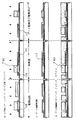
【図1】 本発明によって作製されるトップゲート型TFTを示す上面図。
【図2】 本発明によって作製されるトップゲート型TFTを示す断面図。
【図3】 本発明によって作製されるゲート配線抵抗を改善した配置のトップゲート型TFTを示す上面図。
【図4】 図2及び図3におけるゲート配線を示す断面図。
【図5】 画素部及び駆動回路におけるTFTの作製工程を示す上面図。
【図6】 画素部及び駆動回路におけるTFTの作製工程を示す上面図。
【図7】 画素部及び駆動回路におけるTFTの作製工程を示す上面図。
【図8】 画素部及び駆動回路におけるTFTの作製工程を示す上面図。
【図9】 画素部及び駆動回路におけるTFTの作製工程を示す断面図。
【図10】 画素部及び駆動回路におけるTFTの作製工程を示す断面図。
【図11】 画素部及び駆動回路におけるTFTの作製工程を示す断面図。
【図12】 画素部及び駆動回路におけるTFTの作製工程を示す断面図。
【図13】 アクティブマトリクス型液晶表示装置の作製工程を示す断面図。
【図14】 液晶表示装置の入出力端子、配線、回路配置、スペーサ、シール剤の配置を説明する上面図。
【図15】 液晶表示装置の構造を示す斜視図。
【図16】 携帯型情報端末の一例を示す図。
【図17】 半導体装置の一例を示す図。
【図18】 投影型液晶表示装置の構成を示す図。
【図19】 画素部及び駆動回路におけるTFTの作製工程を示す上面図。
【図20】 画素部及び駆動回路におけるTFTの作製工程を示す上面図。
【図21】 画素部及び駆動回路におけるTFTの作製工程を示す上面図。
【図22】 画素部及び駆動回路におけるTFTの作製工程を示す上面図。
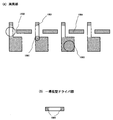
【図23】 導伝性を付与する不純物濃度と、抵抗率の関係。
【図24】 アクティブマトリクス型EL表示装置の回路構成を示す図。
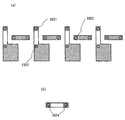
【図25】 画素部におけるTFTの作製工程を示す上面図。[0001]
BACKGROUND OF THE INVENTION
The present invention relates to a semiconductor device having a circuit including a thin film transistor (hereinafter referred to as a thin film transistor) on a substrate having an insulating surface and a manufacturing method thereof. In particular, the present invention relates to an electro-optical device typified by a liquid crystal display device in which a pixel portion and a drive circuit provided in the periphery thereof are provided on the same substrate, and a technique that can be suitably used for an electronic apparatus equipped with the electro-optical device. provide. Note that in this specification, a semiconductor device refers to all devices that function by utilizing semiconductor characteristics, and includes the above-described electro-optical device and electronic devices including the electro-optical device in its category.
[0002]
[Prior art]
As an example of a laminated structure of TFTs of an electro-optical device typified by an active matrix liquid crystal display device, in the case of forming a top gate type, (1) a semiconductor layer, (2) a gate insulating layer, (3) a gate electrode, 5) 5 layers of 4) interlayer insulation layer and (5) source wiring are mentioned. In forming the TFT, (1) separation of the semiconductor layer, (2) formation of the gate insulating layer, (3) formation of the gate electrode, and (4) an interlayer insulating layer corresponding to a location where the wiring is connected to the gate electrode and the source electrode The use of a total of five types of masks, that is, forming an opening in (5) and forming a source wiring (5). The use of a total of five types of masks means that five photolithography steps are performed.
[0003]
The active layer, that is, the semiconductor layer in the TFT is formed on a substrate such as glass by a vapor phase growth method or the like. In recent years, a technology for crystallizing the semiconductor layer of the active layer has progressed, and a TFT having a semiconductor (hereinafter referred to as a crystalline semiconductor) layer (typically crystalline silicon or polycrystalline silicon) including a crystal structure as an active layer. Then, since a high field effect mobility can be obtained, a CMOS circuit composed of an n-channel TFT and a p-channel TFT can be functioned. If a CMOS circuit can be formed, a driving circuit can be integrally formed on the same substrate in addition to the pixel portion, and the use range is large, such as a light weight and thinning in a liquid crystal display device. However, the structure is complicated and the number of processes is increased as compared with the TFT structure of only the n-channel type or the p-channel type.
[0004]
[Problems to be solved by the invention]
As shown above, the TFT fabrication process is many. In particular, when the crystalline semiconductor layer is applied to the active layer and a driver circuit is manufactured in addition to the TFT provided in the pixel portion, the number of the driving circuits increases.
[0005]
One measure of the number of TFT manufacturing processes is the number of photomasks used in the process. A photomask is used in photolithography to form a resist pattern on a substrate as a mask for an etching process. Therefore, the use of a single photomask means that, in addition to steps such as film formation and etching in the steps before and after that, resist stripping, washing and drying steps are added, and even in the photolithography step, It means that complicated steps such as resist coating, pre-baking, exposure, development, and post-baking are performed. It is clear that an increase in the number of processes not only increases the manufacturing cost but also decreases the manufacturing yield.
[0006]
The object of the present invention is to provide means for solving such problems. In other words, by reducing the number of processes, especially by reducing the number of photomasks used in the process, resist coating, pre-baking, exposure, development, and cleaning and drying processes before and after that can be omitted, resulting in significant process reduction as a whole. With the goal.
[0007]
[Means for Solving the Problems]
The present invention provides a technique for reducing the number of photomasks required for manufacturing TFTs and reducing the number of manufacturing processes.
[0008]
In order to solve the above problems, in the present invention, the laminated structure of the top gate type TFT is simplified to a three-layer structure.
That is, in the present invention, a semiconductor layer, an insulating layer on the semiconductor layer, and a conductive layer on the insulating layer are formed on the substrate.
[0009]
In order to form a TFT with the three-layer structure, the source wiring and the gate wiring are formed with the same conductive layer.
[0010]
Retention capacity is 10 19 atomic / cm Three A semiconductor layer to which the above impurities are added, an insulating layer over the semiconductor layer, and a conductive layer over the insulating layer are formed.
[0011]
For gate wiring, an island-shaped conductive layer and 10 19 atomic / cm Three And an island-like semiconductor layer connected to the island-like conductive layer to which the above one-conductivity type impurity is added. A portion intersecting with the source wiring is formed of an island-shaped semiconductor layer, and intersects with an insulating layer. However, since the resistance is expected to increase, the size of the island-like semiconductor layer is made appropriate. Further, as a method for forming the storage capacitor wiring, a method of connecting to the gate wiring and reducing the length of the crossing of the island-like semiconductor layers is given. Details of this will be given in the embodiment of the invention.
[0012]
According to this means, a semiconductor device having a TFT in which a gate wiring and a source wiring cross each other is manufactured with a three-layer structure.
[0013]
In the manufacturing process, the photomask is used for (1) formation of an island-shaped semiconductor layer, (2) formation of a one-conductivity type impurity region, (3) formation of an insulating layer, and (4) formation of a conductive layer. It is used for, ie, a total of 4 sheets.
[0014]
By using such means, the structure of the present invention is a semiconductor device in which a TFT is provided on a substrate. On a first insulating surface, a channel region, a source region, a drain region, the channel region, and the source are provided. A first island-like semiconductor layer that forms a region between regions, a region between the channel region and the drain region, and a region that forms a storage capacitor; and a second island on the first insulating surface A first semiconductor layer and a second insulating surface formed above the first insulating surface, intersecting the channel region and electrically connected to the second island-shaped semiconductor layer; One wiring and a second wiring that overlaps with the region for forming the storage capacitor on the second insulating surface and intersects the second island-shaped semiconductor layer, and the source region, A drain region, a region for forming the storage capacitor, and Said second island-shaped semiconductor layer, 10 19 atomic / cm Three One conductivity type impurity having the above concentration is added.
[0015]
According to another aspect of the present invention, there is provided a semiconductor device in which a TFT is provided over a substrate, a channel region, a source region, a drain region, and a region between the channel region and the source region on the first insulating surface. A first island-shaped semiconductor layer that forms a region between the channel region and the drain region, a region that forms a storage capacitor, and a second island-shaped semiconductor layer on the first insulating surface; A first wiring crossing the channel region and electrically connected to the second island-shaped semiconductor layer on a second insulating surface formed above the first insulating surface; A second wiring that overlaps with a region that forms the storage capacitor on the second insulating surface and that is electrically connected to the first wiring adjacent to the first wiring; and Forming a source region, a drain region, and a storage capacitor; Band, and the second island-shaped semiconductor layer, 10 19 atomic / cm Three One conductivity type impurity having the above concentration is added.
[0016]
A structure relating to a method for manufacturing a semiconductor device of the present invention is a first method for forming a semiconductor layer including a crystal structure on a substrate in the method for manufacturing a semiconductor device having a p-channel TFT and an n-channel TFT on a substrate. A second step of selectively etching the semiconductor layer including the crystal structure to form a first island-like semiconductor layer and a second island-like semiconductor layer; and Add impurity element to give n-type and add 10 19 atomic / cm Three A third step of selectively forming an n-type impurity region having the above concentration; a fourth step of forming an insulating layer on the first island-like semiconductor layer and the second island-like semiconductor layer; A fifth step of selectively etching the insulating layer; and an impurity element imparting p-type conductivity is added to the second island-shaped semiconductor layer. 19 atomic / cm Three A sixth step of selectively forming a p-type impurity region having the above concentration; and a first step of forming a conductive layer on the insulating layer or the first island-shaped semiconductor layer and the second island-shaped semiconductor layer. Step 8, the eighth step of selectively etching the conductive layer, and the first island-like semiconductor layer or the second island-like semiconductor layer passing through the insulating layer to achieve one conductivity type The impurity element is added to activate the impurity element added to the first island-shaped semiconductor layer and the second island-shaped semiconductor layer, and a ninth step of forming a one-conductivity type impurity region. And a tenth step.
[0017]
In another method for manufacturing a semiconductor device having a p-channel TFT and an n-channel TFT over a substrate, the first step of forming a semiconductor layer with an amorphous structure over the substrate A second step of adding any of nickel, iron, palladium, tin, lead, cobalt, platinum, copper, and gold to the non-crystalline semiconductor layer, and heat-treating the semiconductor layer to include a crystalline structure A third step of forming a semiconductor layer; a fourth step of selectively etching the semiconductor layer including the crystal structure to form a first island-like semiconductor layer and a second island-like semiconductor layer; Selectively adding phosphorus or an impurity element imparting phosphorus and n-type to the first island-like semiconductor layer 10 19 atomic / cm Three A fifth step of forming an n-type impurity region of the above concentration, a sixth step of forming an insulating layer on the first island-like semiconductor layer and the second island-like semiconductor layer, and the insulation A seventh step of selectively etching the layer; and the second island-like semiconductor layer is selectively etched with phosphorus and 10 19 atomic / cm Three An eighth step of forming a region to which an impurity imparting p-type at the above concentration is added; and a ninth step of heat-treating or laser-irradiating the first island-like semiconductor layer and the second island-like semiconductor layer. A tenth step of forming a conductive layer on the insulating layer or the first island-like semiconductor layer and the second island-like semiconductor layer, and an eleventh step of selectively etching the conductive layer. And the step of forming an n-type impurity region by adding an impurity element which passes through the insulating layer and imparts n-type to the first island-like semiconductor layer and the second island-like semiconductor layer. And a thirteenth step of activating the impurity element added to the first island-like semiconductor layer and the second island-like semiconductor layer.
[0018]
In another method for manufacturing a semiconductor device in which an n-channel or p-channel TFT is provided over a substrate, a first step of forming a semiconductor layer including a crystal structure over the substrate is provided. A second step of selectively etching the semiconductor layer including the crystal structure to form a plurality of island-like semiconductor layers; and 19 atomic / cm Three A third step of forming the n-channel or p-channel impurity region having the above concentration, a fourth step of forming an insulating layer on the island-like semiconductor layer, and selectively forming the insulating layer. A fifth step of etching; a sixth step of forming a conductive layer on the insulating layer or the island-shaped semiconductor layer; a seventh step of selectively etching the conductive layer; and the island-shaped semiconductor. An eighth step of adding an impurity element of one conductivity type through the insulating layer to selectively form the impurity region of the one conductivity type, and an impurity added to the island-shaped semiconductor layer; And a ninth step of activating the element.
[0019]
In another method for manufacturing a semiconductor device in which an n-channel or p-channel TFT is provided over a substrate, the first step of forming an amorphous semiconductor layer over the substrate A second step of adding any of nickel, iron, palladium, tin, lead, cobalt, platinum, copper, and gold to the non-crystalline semiconductor layer, and heat-treating the semiconductor layer to include a crystalline structure A third step of forming a semiconductor layer; a fourth step of selectively etching the semiconductor layer including the crystal structure to form a plurality of island-shaped semiconductor layers; and , Phosphorus or phosphorus and 10 19 atomic / cm Three A fifth step of forming a one-conductivity type impurity region of the above concentration, a sixth step of forming an insulating layer on the island-like semiconductor layer, and a seventh step of selectively etching the insulating layer Selecting the conductive layer, an eighth step of heat-treating or laser-irradiating the island-shaped semiconductor layer, a ninth step of forming a conductive layer on the insulating layer or the island-shaped semiconductor layer, and the conductive layer A tenth step of selectively etching, an eleventh step of forming the one-conductivity type impurity region through the insulating layer in the island-shaped semiconductor layer, and an impurity added to the island-shaped semiconductor layer And a twelfth step of activating the element.
[0020]
In another method for manufacturing a semiconductor device having a p-channel TFT and an n-channel TFT on a substrate, a first step of forming a semiconductor layer including a crystal structure on the substrate is provided. A second step of selectively etching the semiconductor layer including the crystal structure to form the first island-like semiconductor layer and the second island-like semiconductor layer; and Optionally, an impurity element imparting n-type is added to add 10 19 atomic / cm Three A third step of forming an n-type impurity region of the above concentration, a fourth step of forming an insulating layer on the first island-like semiconductor layer and the second island-like semiconductor layer, and the insulation A fifth step of selectively etching the layer and the second island-like semiconductor layer, 19 atomic / cm Three A sixth step of forming a p-type impurity region having the above concentration; a seventh step of activating the impurity element added to the first island-like semiconductor layer and the second island-like semiconductor layer; An eighth step of forming a conductive layer on the insulating layer or the first island-shaped semiconductor layer and the second island-shaped semiconductor layer; a ninth step of selectively etching the conductive layer; It is characterized by having.
[0021]
In another method for manufacturing a semiconductor device having a p-channel TFT and an n-channel TFT over a substrate, the first step of forming a semiconductor layer with an amorphous structure over the substrate A second step of adding any of nickel, iron, palladium, tin, lead, cobalt, platinum, copper, and gold to the non-crystalline semiconductor layer, and heat-treating the semiconductor layer to include a crystalline structure A third step of forming a semiconductor layer; a fourth step of selectively etching the semiconductor layer including the crystal structure to form the first island-like semiconductor layer and the second island-like semiconductor layer; Then, phosphorus or an impurity element imparting phosphorus and n-type is selectively added to the first island-shaped semiconductor layer. 19 atomic / cm Three A fifth step of forming an n-type impurity region of the above concentration, a sixth step of forming an insulating layer on the first island-like semiconductor layer and the second island-like semiconductor layer, and the insulation A seventh step of selectively etching the layer; and the second island-like semiconductor layer is selectively etched with phosphorus and 10 19 atomic / cm Three An eighth step of forming a region to which the p-type impurity having the above concentration is added; and a ninth step of activating the impurity element added to the first island-like semiconductor layer and the second island-like semiconductor layer. A tenth step of forming a conductive layer on the insulating layer or the first island-like semiconductor layer and the second island-like semiconductor layer, and an eleventh step of selectively etching the conductive layer. The process is characterized by comprising:
[0022]
In another method for manufacturing a semiconductor device in which an n-channel or p-channel TFT is provided over a substrate, a first step of forming a semiconductor layer including a crystal structure over the substrate is provided. A second step of selectively etching the semiconductor layer including the crystal structure to form a plurality of island-like semiconductor layers; and 19 atomic / cm Three A third step of forming a one-conductivity type impurity region having the above-mentioned concentration; a fourth step of activating an impurity element added to the island-shaped semiconductor layer; and insulation on the island-shaped semiconductor layer. A fifth step of forming a layer; a sixth step of selectively etching the insulating layer; a seventh step of forming a conductive layer on the insulating layer or the island-like semiconductor layer; And an eighth step of selectively etching the layer.
[0023]
In another method for manufacturing a semiconductor device in which an n-channel or p-channel TFT is provided over a substrate, the first step of forming an amorphous semiconductor layer over the substrate A second step of adding any of nickel, iron, palladium, tin, lead, cobalt, platinum, copper, and gold to the non-crystalline semiconductor layer, and heat-treating the semiconductor layer to include a crystalline structure A third step of forming a semiconductor layer; a fourth step of selectively etching the semiconductor layer including the crystal structure to form a plurality of island-shaped semiconductor layers; and , Phosphorus or phosphorus and 10 19 atomic / cm Three A fifth step of forming a one-conductivity type impurity region of the above concentration, a sixth step of activating an impurity element added to the island-like semiconductor layer, and insulating on the island-like semiconductor layer A seventh step of forming a layer; an eighth step of selectively etching the insulating layer; a ninth step of forming a conductive layer on the insulating layer or the island-like semiconductor layer; And a tenth step of selectively etching the layer.
[0024]
DETAILED DESCRIPTION OF THE INVENTION
An embodiment of the present invention will be described with reference to FIGS.
[0025]
An example of the structure of a top gate TFT manufactured according to the present invention is shown as a top view in FIG. FIG. 1 shows an example in which an active matrix LCD to which the present invention is applied has a configuration in which the line width is sufficiently large and the number of pixels is sufficiently small, and it is not necessary to consider the resistance of the gate wiring. Moreover, it is set as the structure used for a reflection type liquid crystal display device.
[0026]
FIG. 1A is a top view illustrating the configuration of the pixel portion. The source region of the
[0027]
A
[0028]
In addition, the gate electrode and the gate wiring constituting the TFT are formed of the
[0029]
FIG. 1B is a top view showing the configuration of the n-type TFT in the drive circuit. A
[0030]
FIG. 1C is a top view showing the configuration of the p-type TFT in the drive circuit.
[0031]
2 (a), FIG. 2 (b), and FIG. 2 (c) are cross-sectional views of portions indicated by broken lines A1 to A2, broken lines B1 to B2, and broken lines C1 to C2, respectively, in FIG. . A portion indicated by broken lines A1 to A2 is a drive circuit portion, and an n-type TFT and a p-type TFT are arranged for convenience of explanation.
[0032]
The n-
[0033]
The p-
[0034]
The
[0035]
The shape of the above offset region or LDD region is designed according to the required characteristics. For example, in the P-type TFT of the drive circuit, the distance between the source or drain portion and the channel portion is suitably 2 μm or less, and if it is longer than this, the on-current becomes small.
[0036]
A gate electrode and
[0037]
However, the configuration shown in FIG. 1 is applicable only when the line width of the wiring is large and the resistance of the gate wiring is sufficiently small. In a miniaturized configuration, a device is required for arrangement.
[0038]
As shown in FIG. 3A, the gate wiring has a chain shape of a
[0039]
10 we created twenty one atoms / cm Three The resistivity of the silicon layer to which about phosphorus is added is 2 × 10 after processing. Three It becomes around Ωcm. Resistivity is 2 × 10 Three The semiconductor layer of about Ωcm is about three orders of magnitude larger than the resistivity of Al, which is widely used as a conductive wiring, is about 4 μΩcm. In addition, while the Al conductive wiring is formed with a thickness of 400 nm, the semiconductor layer is often formed with a smaller film thickness for reasons such as crystallization.
[0040]
That is, the resistance is expected to be larger than that of a conventional gate wiring formed only of a conductive material, and it is particularly necessary to examine the line width of the semiconductor layer having a high concentration of impurities. For example, in a direct-view LCD with a pixel pitch of 42 × 126 μm, if the resistance of the conductive wiring and the contact resistance are assumed to be 0 and the thickness of the semiconductor layer is assumed to be 50 nm, the n-type necessary for driving is added. The line width of the
[0041]
Further, as shown in FIG. 3B, the
[0042]
That is, if the circuit in the vicinity of the pixel is formed as shown in FIG. 3B, the resistance can be reduced.
[0043]
The conductivity characteristics when phosphorus is added to the polycrystalline silicon layer are shown in FIG. 23 (MM Mandurah, J. Electrochem. Soc. 126.1019-1023 (June. 1979)). As shown by the poly-crystalline silicon curve in the figure, the phosphorus concentration is 10 19 atoms / cm Three The change in resistivity is different between before and after. Ten 19 atoms / cm Three As it becomes smaller, carriers are trapped at the grain boundaries, the number of carriers in the crystal decreases, and the resistance increases. Ten 19 atoms / cm Three However, the resistivity decreases as the phosphorus concentration increases. 19 atoms / cm Three It becomes gentle compared to smaller changes.
[0044]
10 we created twenty one atoms / cm Three The resistivity of the silicon layer doped with about phosphorus is 2 × 10 Three It becomes around Ωcm. Although this is added at a large concentration for the purpose of reducing the resistivity, a slight increase in resistance is allowed depending on the circuit design. In a conventional TFT, 10 added to the source and drain regions. 19 atoms / cm Three Because there are many of the above, we have not only phosphorus but also impurity elements in the polycrystalline silicon. 19 atoms / cm Three If it was added as described above, it was considered possible to make silicon conductive. 10 added to this silicon 19 atoms / cm Three The above impurity concentration is referred to as high concentration in this specification.
[0045]
The liquid crystal display device operable with the above configuration will be evaluated. When the semiconductor layer is crystallized, a CMOS circuit can be manufactured. At this time, an off-leakage current can be reduced by providing an offset region or an LDD region in all elements. However, when a drive circuit composed of a P-type TFT is formed, the on-current is expected to be small due to the offset region or LDD region. Table 1 shows ON current values when the offset region or the LDD region is formed in a TFT having a width of 8 μm × 8 μm.
[0046]
[Table 1]
In the shift register, transistors corresponding to the number of pixels in one direction are connected. When the number of pixels in one direction is constant, when the shift register is driven at a small ON current value and at a high frequency, the TFT cannot be charged or discharged and no signal flows. Therefore, the frequency is limited by the ON current value. In the pixel portion, the metal portion and the semiconductor portion of the gate wiring are connected in series, and a signal delay occurs due to this increase in resistance. When a signal delay occurs, the effective time of the signal applied to the gate electrode is shortened, and this can be solved by dividing the video signal.
[0048]
In consideration of the operation limit of the shift register, the amount of impurities in the offset region or LDD region and the width of the offset region or LDD region for flowing a necessary on-current were estimated by simulation. In the present invention, the number of pixels is 640 × 3 (RGB) × 480, the pixel pitch is 42 μm × 126 μm, a drive circuit including a p-type TFT and an n-type TFT is provided in the periphery, and corresponds to a video signal divided into four. Take an electro-optical device for liquid crystal display as an example. As a result, regarding the shift register, according to simulation, it was estimated that the shift register operates at a driving frequency of 5 MHz or less. At this time, when the impurity of the LDD region is an impurity imparting n-type, the width of the LDD region operates at 0.5 μm or less, and when the impurity of p-type is imparted, the width of the LDD region is estimated to be 1 μm or less. It was.
[0049]
Thus, the liquid crystal drive circuit of 4 inches square and 5 MHz or less, which is normally mass-produced, operates even in the design according to the present invention.
[0050]
Below, four examples of the manufacturing process of the TFT of the present invention are shown. In Process Example 1, an n-channel TFT and a p-channel TFT are formed on the substrate, and an LDD region is formed on all TFTs. In Process Example 2, an n-channel TFT and a p-channel TFT are formed on the substrate. An example of a process for forming TFTs and forming offset regions in all TFTs. In Process Example 3, an example of forming n-channel TFTs or p-channel TFTs on a substrate and forming LDD regions in all TFTs.
[0051]
(Process example 1)
Table 2 shows a manufacturing process of the TFT of the present invention. Table 2 shows a process example in which a semiconductor layer is crystallized using a metal impurity and LDD regions are formed in all TFTs formed on the substrate. This process will be described by taking the TFT configuration of FIG. 1 as an example in which the storage capacitor wiring intersects with a portion of the gate electrode made of a semiconductor layer doped with high-concentration n-type impurities through an insulating layer. The process order and conditions can also be applied to the structure shown in FIG. 3B in which the storage capacitor wiring is connected to the gate wiring on the opposite side of the direction of the gate wiring of the TFT connected to the storage capacitance wiring. . In Table 2, * is attached to processes using a photomask.
[0052]
[Table 2]
Hereinafter, it will be described with reference to FIGS. 5 to 8 are top views showing the shapes of the layers formed as the process proceeds.
[0054]
The substrate is made of glass or quartz. In the case of glass, it is desirable to form a base film such as a silicon oxide film in order to prevent diffusion of alkali metal or the like from the surface.
[0055]
First, as shown in
[0056]
Next, as shown in Step 2, the amorphous semiconductor layer is crystallized. This may be thermal crystallization, laser crystallization, or a combination thereof. In the present invention, the semiconductor layer can be added by using a metal impurity as a catalyst to promote crystallization. Nickel is effective as the metal impurity, and examples using nickel will be given below. When nickel is added, thermal crystallization is performed in the subsequent step 8, and then a high concentration impurity is doped in the source and drain portions of the P-type TFT portion, and then gettering heat treatment is performed.
[0057]
Next, as shown in step 3, a photoresist is formed on the crystallized semiconductor layer and is formed by dry etching. At this time, as shown in FIG. 5A, the TFT channel and the low-concentration
[0058]
Next, as shown in
[0059]
Then, as shown in step 5, the heavily doped n-type impurity doped region is doped in a region where the mask for doping is not formed in the semiconductor layer. Typically, phosphorus (P) or arsenic (As) is used as the n-type impurity, but phosphorus (P) is used when crystallization is performed using nickel. Because, when adding a catalyst, that is, nickel to the semiconductor layer and crystallizing the semiconductor layer, phosphorus in the semiconductor layer in the channel portion is removed by a method of segregating in a region to which phosphorus is added by heat treatment in a later step. That is, the gettering method is generally taken. This is also used in the present invention.
[0060]
Next, as shown in step 6, an oxide film or a nitride film is formed on the gate insulating layer by plasma CVD, sputtering, thermal oxidation, or the like.
[0061]
Then, as shown in step 7, a photoresist is formed on the gate insulating layer, and an opening is provided by dry etching. FIG. 6 shows the shape of the opening. When a photoresist is formed in the
[0062]
Then, the semiconductor layer is exposed at the portion where the opening is provided. This exposed region is doped with a high concentration of p-type impurity as shown in step 8. When the semiconductor layer is silicon, boron is typically used. In FIG. 6, the region doped with boron is shown by hatching different from the hatching showing the high-concentration n-type impurity. At this time, the
[0063]
Therefore, either before or after doping the p-type impurity, phosphorus is added to the p-type impurity doping region at a concentration not exceeding the p-type impurity concentration. Thereafter, gettering heat treatment is performed. At this time, nickel is gettered to the source and drain regions of each TFT.
[0064]
Then, as shown in Step 9, a conductive wiring is formed by sputtering film formation or the like. This is because the gate wiring and the source wiring need to be in contact with the semiconductor layer to ensure conductivity, so that a material that does not diffuse into the semiconductor layer due to heat and does not increase in resistivity is desirable. Further, since the conductive wiring is in contact with the semiconductor layer, an etching selection ratio between the semiconductor layer and the wiring material when etching in a later process is required. When the semiconductor layer is silicon, it is desirable to etch the wiring material with a chemical solution in order to increase the selection ratio. Based on the above conditions, the conductive wiring material includes Mo and Ag—Pd—Cu, in addition to the lamination of Ti and Al.
[0065]
Thereafter, as shown in
[0066]
At this time, in the semiconductor layer of the pixel portion TFT, when the substrate plane is viewed from above, there is an
[0067]
Thereafter, as shown in step 12, the substrate is treated by laser irradiation or heat-treated at around 500 ° C. As a result, n-type impurities or p-type impurities in the semiconductor are placed in a stable position, and a fixed impurity level is formed. Then, the substrate is heat-treated in a hydrogen atmosphere, and dangling bonds in the semiconductor or between the semiconductor and the gate insulating layer are terminated with hydrogen. This eliminates the interface state and improves the characteristics.
[0068]
Through the above steps, a top-gate TFT using a crystallized semiconductor layer is completed with four masks.
[0069]
(Process example 2)
Table 3 shows a manufacturing process of the TFT of the present invention. Process example 2 shows a process example in which offset regions are formed in all TFTs formed on the substrate. This process will be described by taking as an example a TFT configuration in which a storage capacitor wiring intersects with a portion made of a semiconductor layer to which a high-concentration n-type impurity is added through an insulating layer. The process order and conditions can also be applied to the case where the storage capacitor wiring is connected to the gate wiring on the side opposite to the direction of the gate wiring of the TFT connected to the storage capacitor wiring.
[0070]
[Table 3]
In the process example of Table 3, the process similar to the process example 1 is performed from the
[0072]
At this time, in the semiconductor layer of the pixel portion TFT, when the substrate plane is viewed from above, there is an
[0073]
Then, conductive wiring is formed as shown in
[0074]
Thereafter, as shown in step 12, the substrate is heat-treated in a hydrogen atmosphere, and dangling bonds in the semiconductor or between the semiconductor and the gate insulating layer are terminated with hydrogen. This eliminates the interface state and improves the characteristics. If the semiconductor properties are good without hydrogenation, this step may be omitted.
[0075]
Through the above steps, a top-gate TFT using a crystallized semiconductor layer is completed with four masks.
[0076]
(Process example 3)
Table 4 shows a manufacturing process of the TFT of the present invention. Table 4 shows a process example in which a semiconductor layer is crystallized using a metal impurity, an n-channel TFT or a p-channel TFT is formed on a substrate, and an LDD region is formed in the TFT. This process will be described by taking as an example a TFT configuration in which a storage capacitor wiring intersects with a portion made of a semiconductor layer to which a high-concentration n-type impurity is added through an insulating layer. The process order and conditions can also be applied to the case where the storage capacitor wiring is connected to the gate wiring on the side opposite to the direction of the gate wiring of the TFT connected to the storage capacitor wiring.
[0077]
[Table 4]
Hereinafter, it will be described with reference to FIGS. 19 to 22 are top views showing the shapes of the respective layers formed as the process proceeds.
[0079]
In the process example of Table 4, the process similar to the process example 1 is performed from the
Then, as shown in step 3, a photoresist is formed on the crystallized semiconductor layer, and is formed into an island shape by dry etching. At this time, as shown in FIG. 19A, the TFT channel and low-concentration
[0080]
Next, as shown in
[0081]
Then, as shown in Step 5, the one-conductivity-type impurity-doped region with a high concentration is doped in a region where the mask for doping is not formed in the semiconductor layer. When the semiconductor layer is silicon, if the n-channel TFT or the p-channel TFT is an n-type TFT, typically phosphorous (P) or arsenic (As) is used. Phosphorus (P) is used for the conversion. In addition, in the crystallization of the semiconductor layer, when the semiconductor layer is crystallized using nickel, if the n-channel TFT or the p-channel TFT is p-type, the impurity exceeds the impurity in addition to the impurity. Add phosphorus at no concentration. This is because phosphorus is effective in gettering nickel. Thereafter, gettering heat treatment is performed. At this time, nickel is gettered to the source and drain regions of each TFT.
[0082]
Thereafter, as shown in step 6, an oxide film or a nitride film is formed on the gate insulating layer by plasma CVD, sputtering, thermal oxidation, or the like.
[0083]
Next, as shown in step 7, a photoresist is formed on the gate insulating layer, and an opening is provided by dry etching. FIG. 20 shows the shape of the opening. Openings are provided in the
[0084]
Then, as shown in step 8, a conductive wiring is formed by sputtering film formation or the like. This is because the gate wiring and the source wiring need to be in contact with the semiconductor layer to ensure conductivity, so that a material that does not diffuse into the semiconductor layer due to heat and does not increase in resistivity is desirable. Further, since the conductive wiring is in contact with the semiconductor layer, an etching selection ratio between the semiconductor layer and the wiring material when etching in a later process is required. When the semiconductor layer is silicon, it is desirable to etch the wiring material with a chemical solution in order to increase the selection ratio. Based on the above conditions, the conductive wiring material includes Mo and Ag—Pd—Cu, in addition to the lamination of Ti and Al.
[0085]
Thereafter, as shown in Step 9, a photoresist is formed on the conductive wiring, and the shape of the conductive wiring as shown in FIG. 21 is formed. A
[0086]
At this time, in the semiconductor layer of the pixel portion TFT, when the substrate plane is viewed from above, an
[0087]
Thereafter, as shown in step 11, the substrate is processed by laser irradiation or heat treatment. As a result, the one-conductivity type impurity in the semiconductor is settled in a stable position, and a fixed impurity level is formed. Then, the substrate is heat-treated in a hydrogen atmosphere, and dangling bonds in the semiconductor or between the semiconductor and the gate insulating layer are terminated with hydrogen. This eliminates the interface state and improves the characteristics. If the semiconductor properties are good without hydrogenation, this step may be omitted.
[0088]
Through the above steps, a top-gate TFT using a crystallized semiconductor layer is completed with four masks.
[0089]
(Process example 4)
Table 5 shows a manufacturing process of the TFT of the present invention. Table 5 shows a process example in which a semiconductor layer is crystallized using a metal impurity, an n-channel TFT or a p-channel TFT is formed on a substrate, and an offset region is formed in the TFT. This process will be described by taking as an example a TFT configuration in which a storage capacitor wiring intersects with a portion made of a semiconductor layer to which a high-concentration n-type impurity is added through an insulating layer. The process order and conditions can also be applied to the case where the storage capacitor wiring is connected to the gate wiring on the side opposite to the direction of the gate wiring of the TFT connected to the storage capacitor wiring.
[0090]
[Table 5]
Hereinafter, it will be described with reference to FIGS. 19 to 22 are top views showing the shapes of the respective layers formed as the process proceeds.
[0092]
In the process example of Table 5, the process similar to the process example 3 is performed from the
[0093]
Thereafter, as shown in step 6, the substrate is processed by laser irradiation or heat treatment. As a result, the impurities in the semiconductor are kept in a stable position, and a fixed impurity level is formed.
[0094]
Next, as shown in step 7, an oxide film or a nitride film is formed on the gate insulating layer by plasma CVD, sputtering, thermal oxidation, or the like.
[0095]
Then, as shown in step 8, a photoresist is formed on the gate insulating layer, and an opening is provided by dry etching. FIG. 20 shows the shape of the opening. Openings are provided in the
[0096]
Then, as shown in step 9, a conductive wiring is formed by sputtering film formation or the like. This is because the gate wiring and the source wiring need to be in contact with the semiconductor layer to ensure conductivity, so that a material that does not diffuse into the semiconductor layer due to heat and does not increase in resistivity is desirable. Further, since the conductive wiring is in contact with the semiconductor layer, an etching selection ratio between the semiconductor layer and the wiring material when etching in a later process is required. When the semiconductor layer is silicon, it is desirable to etch the wiring material with a chemical solution in order to increase the selection ratio. Based on the above conditions, the conductive wiring material includes Mo and Ag—Pd—Cu, in addition to the lamination of Ti and Al.
[0097]
Thereafter, as shown in
[0098]
At this time, in the semiconductor layer of the pixel portion TFT, when the substrate plane is viewed from above, an
[0099]
Then, the substrate is heat-treated in a hydrogen atmosphere, and dangling bonds in the semiconductor or between the semiconductor and the gate insulating layer are terminated with hydrogen. This eliminates the interface state and improves the characteristics. If the semiconductor properties are good without hydrogenation, this step may be omitted.
[0100]
Through the above steps, a top-gate TFT using a crystallized semiconductor layer is completed with four masks.
[0101]
Further, according to the present invention, not only a liquid crystal display device having a TFT provided in a pixel portion but also a semiconductor device having a p-channel TFT and an n-channel TFT, or an n-channel TFT or a p-channel TFT is provided. A semiconductor device having the same can be manufactured.
[0102]
【Example】
A detailed description will be given with reference to the following examples.
[0103]
[Example 1]
An embodiment of the present invention will be described with reference to FIGS. 9 to 12, cross sections A1 to A2 in FIG. 2 are used as TFTs of a drive circuit provided in the periphery of the pixel portion, and cross sections A1 to A2 in FIG. 2 are used as TFTs and storage capacitors provided in the pixels. The cross sections A1 to A2 in the middle are shown as the gate wiring and the gate electrode portion, and a method for simultaneously manufacturing them will be described in detail according to the steps. Note that resist portions formed by photolithography are shown as PM1 to PM4 in the drawing.
[0104]
In FIG. 9A, a
[0105]
The silicon oxynitride film is formed by using a conventional parallel plate type plasma CVD method. The silicon oxynitride film 102a is made of SiH. Four 10SCCM, NH Three To 100 SCCM, N 2 O was introduced into the reaction chamber as 20 SCCM, the substrate temperature was 325 ° C., the reaction pressure was 40 Pa, and the discharge power density was 0.41 W / cm. 2 The discharge frequency was 60 MHz. On the other hand, the silicon oxynitride silicon film 102b is made of SiH. Four 5SCCM, N 2 O for 120 SCCM, H 2 Was introduced into the reaction chamber as 125 SCCM, the substrate temperature was 400 ° C., the reaction pressure was 20 Pa, and the discharge power density was 0.41 W / cm. 2 The discharge frequency was 60 MHz. These films can be formed continuously only by changing the substrate temperature and switching the reaction gas.
[0106]
Next, a
[0107]
Then, a crystallization step is performed to form a
[0108]
In the process of forming an amorphous silicon film by plasma CVD, SiH is used as a reactive gas. Four And argon (Ar) and the substrate temperature during film formation is set to 400 to 450 ° C., the hydrogen concentration of the amorphous silicon film can be reduced to 5 atomic% or less. In such a case, heat treatment for releasing hydrogen is not necessary.
[0109]
When crystallization is performed by laser annealing, a pulse oscillation type or continuous light emission type excimer laser or argon laser is used as the light source. In the case of using a pulse oscillation type excimer laser, laser annealing is performed by processing laser light into a linear shape. The laser annealing conditions are appropriately selected by the practitioner. For example, the laser pulse oscillation frequency is 30 Hz, and the laser energy density is 100 to 500 mJ / cm. 2 (Typically 300-400mJ / cm 2 ). Then, a linear beam is irradiated over the entire surface of the substrate, and the linear beam superposition ratio (overlap ratio) at this time is set to 80 to 98%. In this way, a
[0110]
Then, using the first photomask over the
[0111]
For such an island-shaped semiconductor layer, an impurity element imparting p-type conductivity is used in order to control the threshold voltage (Vth) of the TFT. 16 ~ 5x10 17 atomic / cm Three You may add to the whole surface of an island-like semiconductor layer with a density | concentration of a grade. As an impurity element imparting p-type to a semiconductor, elements of Group 13 of the periodic table such as boron (B), aluminum (Al), and gallium (Ga) are known. As the method, an ion implantation method or an ion doping method (or an ion shower doping method) can be used, but the ion doping method is suitable for processing a large area substrate. In the ion doping method, diborane (B 2 H 6 ) As a source gas and boron (B) is added. Such implantation of the impurity element is not always necessary and may be omitted. However, this is a technique that is particularly suitable for keeping the threshold voltage of the n-channel TFT within a predetermined range.
[0112]
Then, as shown in FIG. 10D, a resist is formed using a second photomask, a first doping process is performed, and an impurity element imparting n-type conductivity is added. The doping method may be an ion doping method or an ion implantation method. The condition of the ion doping method is a dose of 1 × 10 14 ~ 5x10 15 atomic / cm 2 And an acceleration voltage of 5 to 15 keV. As an impurity element imparting n-type, an element belonging to Group 15, typically phosphorus (P) or arsenic (As), is used here, but phosphorus (P) is used. The first impurity region has 1 × 10 20 ~ 1x10 twenty one atomic / cm Three An impurity element imparting n-type is added in a concentration range of. As a result, the source and driving
[0113]
After the first doping process, a gate insulating film is formed over the semiconductor layer. The
[0114]
Then, a resist mask is formed with a third photomask, and an opening is formed in the insulating film by dry etching as shown in FIG. CHF for dry etching of gate insulating film Three The gas is used.
[0115]
Since the semiconductor is exposed in the opening of the insulating film, an impurity region is formed by doping a high concentration p-type impurity therefrom. This impurity region is diborane (B 2 H 6 The boron (B) concentration in the high-concentration p-type impurity region is 1 × 10 20 ~ 1x10 twenty one atomic / cm Three To be. Thus, a high concentration p-type impurity region 114 which is a source region and a drain region of the island-like semiconductor layer forming the p-channel TFT is formed.
[0116]
At this time, the source and drain regions are also exposed in the island-like semiconductor layer forming the n-channel TFT, and the impurity element imparting the p-type is added. In this p-type impurity region, phosphorus is 3 × 10 4 in the previous step. 20 ~ 3x10 twenty one atomic / cm Three Contained at a concentration of That is, a concentration not exceeding the concentration of the impurity element imparting n-type in the source and drain regions is added, and the electrical characteristics of the n-type impurity region do not change.
[0117]
Then, a conductive metal film is formed by sputtering or vacuum deposition, a resist mask pattern is formed by a fourth photomask, and etching is performed to form a driver circuit and a pixel on the gate insulating film as shown in FIG. The
[0118]
Then, a second doping process is performed. In this case, an impurity element which imparts n-type is doped under a condition of a lower acceleration amount and a higher acceleration voltage than in the first doping treatment. For example, the acceleration voltage is 70 to 120 keV and 1 × 10 13 /cm 2 A new impurity region is formed inside the high-concentration impurity region formed in the island-shaped semiconductor layer in FIG. Doping is performed by setting the acceleration voltage to about 60 to 100 keV and adding an n-type impurity through the insulating film into the semiconductor layer. Thus, a low concentration impurity region is formed between the channel formation region and the high concentration impurity region. The impurity element imparting n-type is 2 × 10 17 ~ 3x10 18 atomic / cm Three So that the concentration becomes.
[0119]
Thereafter, a step of activating the impurity element imparting n-type or p-type added at each concentration is performed. This step is performed by a thermal annealing method using a furnace annealing furnace. In addition, a laser annealing method or a rapid thermal annealing method (RTA method) can be applied. In the thermal annealing method, the oxygen concentration is 1 ppm or less, preferably 0.1 ppm or less in a nitrogen atmosphere at 400 to 700 ° C., typically 500 to 600 ° C. In this example, the temperature is 550 ° C. for 4 hours. Heat treatment was performed. Further, when a plastic substrate having a low heat resistant temperature is used as the
[0120]
Subsequent to the activation step, the step of hydrogenating the island-like semiconductor layer by changing the atmospheric gas and performing heat treatment at 300 to 450 ° C. for 1 to 12 hours in an atmosphere containing 3 to 100% hydrogen. Do. This step is performed on the island-
[0121]
In this way, a substrate having TFTs of a driver circuit and TFTs provided in a pixel portion can be completed on the same substrate by using four photomasks. A p-channel TFT and an n-channel TFT are formed in the driver circuit, and a TFT and a storage capacitor are formed in the pixel portion. In this specification, such a substrate is referred to as an active matrix substrate for convenience.
[0122]
[Example 2]
In this embodiment, another method for manufacturing a crystalline semiconductor layer for forming an active layer of a TFT of the active matrix substrate described in
[0123]
At this time, in the same manner as in Example 1, a base film and a semiconductor layer having an amorphous structure are formed on a glass substrate with a thickness of 25 to 80 nm. The amorphous semiconductor layer includes an amorphous silicon (a-Si) film, an amorphous silicon / germanium (a-SiGe) film, an amorphous silicon carbide (a-SiC) film, and an amorphous silicon / tin (a -SiSn) film or the like can be applied. These amorphous semiconductor layers are preferably formed so as to contain about 0.1 to 40 atomic% of hydrogen. For example, an amorphous silicon film is formed with a thickness of 55 nm. Then, a layer containing the catalytic element is formed by a spin coating method in which an aqueous solution containing 10 ppm of the catalytic element in terms of weight is applied by rotating the substrate with a spinner. Catalyst elements include nickel (Ni), germanium (Ge), iron (Fe), palladium (Pd), tin (Sn), lead (Pb), cobalt (Co), platinum (Pt), copper (Cu), gold (Au). The layer containing the catalytic element may be formed by a printing method, a spray method, a bar coater method, a sputtering method or a vacuum deposition method in addition to the spin coating method to a thickness of 1 to 5 nm. good.
[0124]
In the crystallization step, first, heat treatment is performed at 400 to 500 ° C. for about 1 hour, so that the amount of hydrogen contained in the amorphous silicon film is 5 atomic% or less. When the amount of hydrogen contained in the amorphous silicon film is this value from the beginning after the film formation, this heat treatment is not necessarily required. Then, using a furnace annealing furnace, thermal annealing is performed at 550 to 600 ° C. for 1 to 8 hours in a nitrogen atmosphere. Through the above steps, a crystalline semiconductor layer made of a crystalline silicon film can be obtained. However, when the crystalline semiconductor layer produced by this thermal annealing is observed macroscopically by optical microscope observation, it may be observed that an amorphous region remains locally. Similarly for Raman spectroscopy, 480 cm -1 An amorphous component having a broad peak is observed. Therefore, it can be applied as an effective means to increase the crystallinity of the crystalline semiconductor layer by the laser annealing method described in
[0125]
Similarly, there is a crystallization method using a catalyst element. At this time, a layer containing the catalyst element is formed by a sputtering method. First, in the same manner as in Example 1, a base film and a semiconductor layer having an amorphous structure are formed on a glass substrate with a thickness of 25 to 80 nm. Then, an oxide film (not shown) having a thickness of about 0.5 to 5 nm is formed on the surface of the semiconductor layer having an amorphous structure. The oxide film having such a thickness may be positively formed by a plasma CVD method, a sputtering method, or the like. However, the oxide film is not exposed to a plasma atmosphere by heating the substrate to 100 to 300 ° C. The surface of the semiconductor layer having a crystalline structure may be exposed, or hydrogen peroxide solution (H 2 O 2 ) May be formed by exposing the surface of the semiconductor layer having an amorphous structure. Alternatively, it can be formed by irradiating ultraviolet light in an atmosphere containing oxygen to generate ozone and exposing a semiconductor layer having an amorphous structure to the ozone atmosphere.
[0126]
In this manner, the layer containing the catalytic element is formed by sputtering on the semiconductor layer having an amorphous structure having a thin oxide film on the surface. The thickness of this layer is not limited, but it may be formed to a thickness of about 10 to 100 nm. For example, it is an effective method to form a Ni film using Ni as a target. In the sputtering method, a part of high-energy particles made of the catalytic element accelerated by an electric field also fly to the substrate side, and the oxide film formed near the surface of the semiconductor layer having an amorphous structure or on the surface of the semiconductor layer It is driven in. The ratio varies depending on the plasma generation conditions and the bias state of the substrate, but preferably the amount of the catalytic element implanted in the vicinity of the surface of the semiconductor layer having an amorphous structure or in the oxide film is 1 × 10. 11 ~ 1x10 14 atom / cm 2 It is good to make it to the extent.
[0127]
Thereafter, the layer containing the catalyst element is selectively removed. For example, when this layer is formed of a Ni film, it can be removed with a solution such as nitric acid, or a semiconductor having an Ni film and an amorphous structure if treated with an aqueous solution containing hydrofluoric acid. The oxide film formed on the layer can be removed simultaneously. In any case, the amount of the catalytic element in the vicinity of the surface of the semiconductor layer having an amorphous structure is 1 × 10 11 ~ 1x10 14 atom / cm 2 Try to be about. Then, a crystalline semiconductor layer can be obtained by performing a crystallization process by thermal annealing.
[0128]
If an island-like semiconductor layer is produced from the crystalline semiconductor layer produced in the above process, an active matrix substrate can be completed in the same manner as in Example 1. However, when a catalyst element that promotes crystallization of silicon is used in the crystallization step, a small amount (1 × 10 10) is contained in the island-shaped semiconductor layer. 17 ~ 1x10 19 atomic / cm Three Degree) catalyst element remains. Of course, it is possible to complete the TFT even in such a state, but it is more preferable to remove at least the remaining catalyst element from the channel formation region. One means for removing this catalytic element is a means that utilizes the gettering action of phosphorus (P).
[0129]
The gettering process with phosphorus (P) for this purpose can be performed simultaneously in the activation process. The concentration of phosphorus (P) necessary for gettering may be approximately the same as the impurity concentration of the high-concentration n-type impurity region, and the catalyst from the channel formation region of the n-channel TFT and the p-channel TFT is formed by thermal annealing in the activation process. The element can be segregated to an impurity region containing phosphorus (P) at that concentration. As a result, the impurity region is 1 × 10 17 ~ 1x10 19 atomic / cm Three About a catalytic element segregated. The TFT manufactured in this manner has a low off-current value and good crystallinity, so that high field-effect mobility can be obtained and good characteristics can be achieved.
[0130]
[Example 3]
In this embodiment, an example in which part of the pixel electrode of the active matrix substrate shown in
[0131]
FIG. 25 shows a case where a
[0132]
In this manner, a substrate having a pixel electrode made of a transparent conductive film in the pixel portion can be completed with five photomasks. The active matrix substrate thus produced can be used for a transmissive display device.
[0133]
[Example 4]
In this embodiment, a process of manufacturing an active matrix liquid crystal display device from the active matrix substrate manufactured in
[0134]
First, spacers made of columnar spacers are formed on the active matrix substrate in the state shown in FIG. The spacer may be provided by dispersing particles of several μm, but here, a method of forming a resin film on the entire surface of the substrate and then patterning it is adopted. Although there is no limitation on the material of such a spacer, for example, NN700 manufactured by JSR Co. is used, and after applying with a spinner, a predetermined pattern is formed by exposure and development processing. Further, it is cured by heating at 150 to 200 ° C. using a clean oven or the like.
[0135]
The arrangement of the spacers may be determined arbitrarily. Preferably, as shown in FIG. 13, in the pixel portion, a
[0136]
Thereafter, an
[0137]
A
[0138]
FIG. 14 is a top view of such an active matrix substrate, and is a top view showing the positional relationship between the pixel portion and the drive circuit portion, the spacer, and the sealant. A scanning
[0139]
The
[0140]
The structure of such an active matrix liquid crystal display device will be described with reference to the perspective view of FIG. In FIG. 15, the active matrix substrate includes a
[0141]
A liquid crystal display device having such a structure can be formed using the active matrix substrate shown in
[0142]
[Example 5]
The present invention can also be applied to an active matrix EL display. An example is shown in FIG.
[0143]
FIG. 24 is a circuit diagram of an active matrix EL display.
[0144]
In the active matrix EL display of this embodiment, the CMOS circuit created in the first embodiment is used as the X
[0145]
[Example 6]
An active matrix substrate, a liquid crystal display device, and an EL display device manufactured by implementing the present invention can be used in various electro-optical devices. The present invention can be applied to all electronic devices in which such an electro-optical device is incorporated as a display medium. Examples of electronic devices include personal computers, digital cameras, video cameras, portable information terminals (mobile computers, mobile phones, electronic books, etc.), navigation systems, and the like.
[0146]
FIG. 16A illustrates a portable information terminal which includes a
[0147]
Such portable information terminals are often used outdoors as well as indoors. In order to enable long-term use, a backlight is not used, and a reflective liquid crystal display device that uses outside light is suitable as a low-power consumption type, but a backlight is provided when the surroundings are dark. A transmissive liquid crystal display device is suitable. From such a background, a hybrid type liquid crystal display device having both characteristics of a reflection type and a transmission type has been developed. However, the present invention can also be applied to such a hybrid type liquid crystal display device. A display device 2205 includes a
[0148]
FIG. 16B illustrates a structure of a pixel portion in a hybrid liquid crystal display device, in which a
[0149]
FIG. 17A illustrates a personal computer which includes a
[0150]
FIG. 17B shows a video camera, which includes a
[0151]
FIG. 17D shows a player that uses a recording medium (hereinafter referred to as a recording medium) in which a program is recorded, and includes a main body 2401, a
[0152]
FIG. 17E illustrates a digital camera which includes a
[0153]
FIG. 18A shows a front projector, which includes a light source optical system, a
[0154]
Note that FIG. 18C illustrates an example of the structure of the light source optical system and the
[0155]
Although not shown here, the present invention can be applied to a navigation system, a reading circuit of an image sensor, and the like. As described above, the application range of the present invention is extremely wide and can be applied to electronic devices in various fields. Moreover, the electronic device of a present Example is realizable using the technique of Examples 1-3.
[0156]
【The invention's effect】
In the top gate type TFT, the stacked structure is made of three layers, so that the manufacturing cost can be reduced and the yield can be improved. In the top gate TFT manufacturing process, the number of photomasks is set to four, thereby reducing the manufacturing cost and improving the yield. A top gate TFT used for a reflective active matrix display device can be formed using four photomasks. A top gate TFT used for a transmissive active matrix display device can be formed using five photomasks. Moreover, off-leakage current can be reduced by providing LDD or offset regions in all TFTs to be manufactured.
[Brief description of the drawings]
FIG. 1 is a top view showing a top gate type TFT manufactured according to the present invention.
FIG. 2 is a cross-sectional view showing a top gate type TFT manufactured according to the present invention.
FIG. 3 is a top view showing a top gate type TFT with an improved gate wiring resistance manufactured according to the present invention.
4 is a cross-sectional view showing a gate wiring in FIGS. 2 and 3. FIG.
FIG. 5 is a top view illustrating a manufacturing process of a TFT in a pixel portion and a driver circuit.
FIG. 6 is a top view illustrating a manufacturing process of a TFT in a pixel portion and a driver circuit.
FIG. 7 is a top view illustrating a manufacturing process of a TFT in a pixel portion and a driver circuit.
FIG. 8 is a top view illustrating a manufacturing process of a TFT in a pixel portion and a driver circuit.
FIG. 9 is a cross-sectional view illustrating a manufacturing process of a TFT in a pixel portion and a driver circuit.
FIG. 10 is a cross-sectional view illustrating a manufacturing process of a TFT in a pixel portion and a driver circuit.
FIG. 11 is a cross-sectional view illustrating a manufacturing process of a TFT in a pixel portion and a driver circuit.
12 is a cross-sectional view illustrating a manufacturing process of a TFT in a pixel portion and a driver circuit. FIG.
FIG. 13 is a cross-sectional view illustrating a manufacturing process of an active matrix liquid crystal display device.
14 is a top view illustrating input / output terminals, wiring, circuit layout, spacers, and sealant layout of a liquid crystal display device. FIG.
FIG. 15 is a perspective view illustrating a structure of a liquid crystal display device.
FIG. 16 illustrates an example of a portable information terminal.
FIG 17 illustrates an example of a semiconductor device.
FIG. 18 is a diagram showing a configuration of a projection type liquid crystal display device.
FIG. 19 is a top view illustrating a manufacturing process of a TFT in a pixel portion and a driver circuit.
FIG. 20 is a top view illustrating a manufacturing process of a TFT in a pixel portion and a driver circuit.
FIG. 21 is a top view illustrating a manufacturing process of a TFT in a pixel portion and a driver circuit.
FIG. 22 is a top view illustrating a manufacturing process of a TFT in a pixel portion and a driver circuit.
FIG. 23 shows the relationship between the impurity concentration imparting conductivity and the resistivity.
FIG. 24 is a diagram showing a circuit configuration of an active matrix EL display device.
FIG. 25 is a top view illustrating a manufacturing process of a TFT in a pixel portion.
Claims (3)
前記結晶構造を含む半導体層をエッチングして、チャネル領域と、ソース領域と、ドレイン領域と、保持容量を形成する領域と、を含む第1の島状半導体層と、ゲート配線の一部となる第2の島状半導体層及び第3の島状半導体層と、を形成し、
前記ソース領域、前記ドレイン領域、前記保持容量を形成する領域、前記第2の島状半導体層、及び前記第3の島状半導体層に、n型を付与する不純物元素を添加し、
前記第1の島状半導体層、前記第2の島状半導体層、及び前記第3の島状半導体層上に絶縁層を形成し、
前記絶縁層を選択的にエッチングして、前記ソース領域、前記ドレイン領域、前記第2の島状半導体層、及び前記第3の島状半導体層上の前記絶縁層の一部に開口部を形成し、
前記開口部によって露出した前記ソース領域、前記ドレイン領域、前記第2の島状半導体層、及び前記第3の島状半導体層に、p型を付与する不純物元素を添加し、
前記絶縁層、前記第1の島状半導体層、前記第2の島状半導体層、及び前記第3の島状半導体層上に導電層を形成し、
前記導電層を選択的にエッチングして、ソース配線と、前記第2の島状半導体層と前記第3の島状半導体層を電気的に接続するゲート配線と、を形成し、
前記第1の島状半導体層、前記第2の島状半導体層、及び前記第3の島状半導体層に、前記絶縁層を通過させて前記n型を付与する不純物元素を添加して低濃度不純物領域を形成し、
前記第1の島状半導体層、前記第2の島状半導体層、及び前記第3の島状半導体層に添加された不純物元素を活性化することを特徴とする半導体装置の作製方法。Forming a semiconductor layer including a crystal structure on an insulating surface;
The semiconductor layer including the crystal structure is etched to form a first island-shaped semiconductor layer including a channel region, a source region, a drain region, and a region for forming a storage capacitor, and part of a gate wiring. Forming a second island-shaped semiconductor layer and a third island-shaped semiconductor layer;
An impurity element imparting n-type is added to the source region, the drain region, the region for forming the storage capacitor, the second island-shaped semiconductor layer, and the third island-shaped semiconductor layer,
Forming an insulating layer on the first island-shaped semiconductor layer, the second island-shaped semiconductor layer, and the third island-shaped semiconductor layer;
The insulating layer is selectively etched to form openings in part of the insulating layer on the source region, the drain region, the second island-shaped semiconductor layer, and the third island-shaped semiconductor layer. And
An impurity element imparting p-type is added to the source region, the drain region, the second island-shaped semiconductor layer, and the third island-shaped semiconductor layer exposed by the opening,
Forming a conductive layer on the insulating layer, the first island-shaped semiconductor layer, the second island-shaped semiconductor layer, and the third island-shaped semiconductor layer;
The conductive layer is selectively etched to form a source wiring, and a gate wiring that electrically connects the second island-shaped semiconductor layer and the third island-shaped semiconductor layer,
A low concentration of the first island-shaped semiconductor layer, the second island-shaped semiconductor layer, and the third island-shaped semiconductor layer by adding an impurity element that imparts the n-type through the insulating layer Forming impurity regions ;
A method for manufacturing a semiconductor device, comprising: activating an impurity element added to the first island-shaped semiconductor layer, the second island-shaped semiconductor layer, and the third island-shaped semiconductor layer.
前記非結晶構造の半導体層にニッケルを添加し、
前記非結晶構造の半導体層を熱処理し、結晶構造を含む半導体層を形成し、
前記結晶構造を含む半導体層をエッチングして、チャネル領域と、ソース領域と、ドレイン領域と、保持容量を形成する領域と、を含む第1の島状半導体層と、ゲート配線の一部となる第2の島状半導体層及び第3の島状半導体層を形成し、
前記ソース領域、前記ドレイン領域、前記保持容量を形成する領域、前記第2の島状半導体層、及び前記第3の島状半導体層に、n型を付与する不純物元素を添加し、
前記第1の島状半導体層、前記第2の島状半導体層、及び前記第3の島状半導体層上に絶縁層を形成し、
前記絶縁層を選択的にエッチングして、前記ソース領域、前記ドレイン領域、前記第2の島状半導体層、及び前記第3の島状半導体層上の前記絶縁層の一部に開口部を形成し、
前記開口部によって露出した前記ソース領域、前記ドレイン領域、前記第2の島状半導体層、及び前記第3の島状半導体層に、p型を付与する不純物を添加し、
前記第1の島状半導体層、前記第2の島状半導体層、及び前記第3の島状半導体層を熱処理し、
前記絶縁層、前記第1の島状半導体層、前記第2の島状半導体層、及び前記第3の島状半導体層の上に導電層を形成し、
前記導電層を選択的にエッチングして、ソース配線と、前記第2の島状半導体層と前記第3の島状半導体層を電気的に接続するゲート配線と、を形成し、
前記第1の島状半導体層、前記第2の島状半導体層、及び前記第3の島状半導体層に、前記絶縁層を通過させて前記n型を付与する不純物元素を添加して低濃度不純物領域を形成し、
前記第1の島状半導体層、前記第2の島状半導体層、及び前記第3の島状半導体層に添加された不純物元素を活性化することを特徴とする半導体装置の作製方法。Forming an amorphous semiconductor layer on the insulating surface;
It was added nickel in the semiconductor layer of the non-crystalline structure,
Heat-treating the non-crystalline semiconductor layer to form a semiconductor layer including a crystalline structure;
The semiconductor layer including the crystal structure is etched to form a first island-shaped semiconductor layer including a channel region, a source region, a drain region, and a region for forming a storage capacitor, and part of a gate wiring. Forming a second island-like semiconductor layer and a third island-like semiconductor layer;
An impurity element imparting n-type is added to the source region, the drain region, the region for forming the storage capacitor, the second island-shaped semiconductor layer, and the third island-shaped semiconductor layer,
Forming an insulating layer on the first island-shaped semiconductor layer, the second island-shaped semiconductor layer, and the third island-shaped semiconductor layer;
The insulating layer is selectively etched to form openings in part of the insulating layer on the source region, the drain region, the second island-shaped semiconductor layer, and the third island-shaped semiconductor layer. And
Adding an impurity imparting p-type to the source region, the drain region, the second island-shaped semiconductor layer, and the third island-shaped semiconductor layer exposed by the opening;
Wherein the first island-shaped semiconductor layer, the second island-shaped semiconductor layer, and the third island-shaped semiconductor layer was Netsusho sense,
Forming a conductive layer on the insulating layer, the first island-shaped semiconductor layer, the second island-shaped semiconductor layer, and the third island-shaped semiconductor layer;
The conductive layer is selectively etched to form a source wiring, and a gate wiring that electrically connects the second island-shaped semiconductor layer and the third island-shaped semiconductor layer,
Wherein the first island-shaped semiconductor layer, the second island-shaped semiconductor layer, and the Third island-like semiconductor layer, a low concentration by adding an impurity element imparting the n-type is passed through the insulating layer Forming impurity regions ;
A method for manufacturing a semiconductor device, comprising: activating an impurity element added to the first island-shaped semiconductor layer, the second island-shaped semiconductor layer, and the third island-shaped semiconductor layer.
前記半導体装置は、パーソナルコンピュータ、ビデオカメラ、携帯型情報端末、デジタルカメラ、またはプロジェクターであることを特徴とする半導体装置の作製方法。In claim 1 or claim 2 ,
The method for manufacturing a semiconductor device, wherein the semiconductor device is a personal computer, a video camera, a portable information terminal, a digital camera, or a projector.
Priority Applications (1)
| Application Number | Priority Date | Filing Date | Title |
|---|---|---|---|
| JP2000232507A JP4801242B2 (en) | 2000-07-31 | 2000-07-31 | Method for manufacturing semiconductor device |
Applications Claiming Priority (1)
| Application Number | Priority Date | Filing Date | Title |
|---|---|---|---|
| JP2000232507A JP4801242B2 (en) | 2000-07-31 | 2000-07-31 | Method for manufacturing semiconductor device |
Publications (3)
| Publication Number | Publication Date |
|---|---|
| JP2002050761A JP2002050761A (en) | 2002-02-15 |
| JP2002050761A5 JP2002050761A5 (en) | 2007-09-20 |
| JP4801242B2 true JP4801242B2 (en) | 2011-10-26 |
Family
ID=18725181
Family Applications (1)
| Application Number | Title | Priority Date | Filing Date |
|---|---|---|---|
| JP2000232507A Expired - Fee Related JP4801242B2 (en) | 2000-07-31 | 2000-07-31 | Method for manufacturing semiconductor device |
Country Status (1)
| Country | Link |
|---|---|
| JP (1) | JP4801242B2 (en) |
Families Citing this family (7)
| Publication number | Priority date | Publication date | Assignee | Title |
|---|---|---|---|---|
| US20100224878A1 (en) * | 2009-03-05 | 2010-09-09 | Semiconductor Energy Laboratory Co., Ltd. | Semiconductor device |
| DE112013007566B3 (en) | 2012-08-03 | 2018-02-22 | Semiconductor Energy Laboratory Co., Ltd. | Semiconductor device |
| TWI575663B (en) | 2012-08-31 | 2017-03-21 | 半導體能源研究所股份有限公司 | Semiconductor device |
| CN111477634B (en) | 2012-09-13 | 2023-11-14 | 株式会社半导体能源研究所 | Semiconductor device with a semiconductor device having a plurality of semiconductor chips |
| US9905585B2 (en) | 2012-12-25 | 2018-02-27 | Semiconductor Energy Laboratory Co., Ltd. | Semiconductor device comprising capacitor |
| KR20220145922A (en) | 2012-12-25 | 2022-10-31 | 가부시키가이샤 한도오따이 에네루기 켄큐쇼 | Semiconductor device |
| CN111129039B (en) * | 2013-12-27 | 2024-04-16 | 株式会社半导体能源研究所 | Light emitting device |
Family Cites Families (2)
| Publication number | Priority date | Publication date | Assignee | Title |
|---|---|---|---|---|
| JP3137839B2 (en) * | 1994-07-30 | 2001-02-26 | 株式会社半導体エネルギー研究所 | Active matrix circuit |
| JPH1195256A (en) * | 1997-09-25 | 1999-04-09 | Sharp Corp | Active matrix substrate |
-
2000
- 2000-07-31 JP JP2000232507A patent/JP4801242B2/en not_active Expired - Fee Related
Also Published As
| Publication number | Publication date |
|---|---|
| JP2002050761A (en) | 2002-02-15 |
Similar Documents
| Publication | Publication Date | Title |
|---|---|---|
| US9786787B2 (en) | Semiconductor device and fabrication method thereof | |
| JP4801790B2 (en) | Semiconductor device | |
| US6515336B1 (en) | Thin film transistors having tapered gate electrode and taped insulating film | |
| US9236400B2 (en) | Semiconductor device and manufacturing method thereof | |
| JP4801241B2 (en) | Semiconductor device and manufacturing method thereof | |
| JP4683696B2 (en) | Method for manufacturing semiconductor device | |
| JP4522529B2 (en) | Semiconductor device and manufacturing method thereof | |
| JP4801242B2 (en) | Method for manufacturing semiconductor device | |
| JP3983460B2 (en) | Method for manufacturing semiconductor device | |
| JP4869472B2 (en) | Semiconductor device | |
| JP4637333B2 (en) | Method for manufacturing semiconductor device | |
| JP4712155B2 (en) | Method for manufacturing semiconductor device | |
| JP4202777B2 (en) | Method for manufacturing semiconductor device | |
| JP5244837B2 (en) | Semiconductor device |
Legal Events
| Date | Code | Title | Description |
|---|---|---|---|
| A521 | Written amendment |
Free format text: JAPANESE INTERMEDIATE CODE: A523 Effective date: 20070719 |
|
| A621 | Written request for application examination |
Free format text: JAPANESE INTERMEDIATE CODE: A621 Effective date: 20070719 |
|
| A977 | Report on retrieval |
Free format text: JAPANESE INTERMEDIATE CODE: A971007 Effective date: 20100908 |
|
| A131 | Notification of reasons for refusal |
Free format text: JAPANESE INTERMEDIATE CODE: A131 Effective date: 20100928 |
|
| A521 | Written amendment |
Free format text: JAPANESE INTERMEDIATE CODE: A523 Effective date: 20101117 |
|
| TRDD | Decision of grant or rejection written | ||
| A01 | Written decision to grant a patent or to grant a registration (utility model) |
Free format text: JAPANESE INTERMEDIATE CODE: A01 Effective date: 20110802 |
|
| A01 | Written decision to grant a patent or to grant a registration (utility model) |
Free format text: JAPANESE INTERMEDIATE CODE: A01 |
|
| A61 | First payment of annual fees (during grant procedure) |
Free format text: JAPANESE INTERMEDIATE CODE: A61 Effective date: 20110805 |
|
| FPAY | Renewal fee payment (event date is renewal date of database) |
Free format text: PAYMENT UNTIL: 20140812 Year of fee payment: 3 |
|
| R150 | Certificate of patent or registration of utility model |
Free format text: JAPANESE INTERMEDIATE CODE: R150 |
|
| FPAY | Renewal fee payment (event date is renewal date of database) |
Free format text: PAYMENT UNTIL: 20140812 Year of fee payment: 3 |
|
| R250 | Receipt of annual fees |
Free format text: JAPANESE INTERMEDIATE CODE: R250 |
|
| R250 | Receipt of annual fees |
Free format text: JAPANESE INTERMEDIATE CODE: R250 |
|
| R250 | Receipt of annual fees |
Free format text: JAPANESE INTERMEDIATE CODE: R250 |
|
| R250 | Receipt of annual fees |
Free format text: JAPANESE INTERMEDIATE CODE: R250 |
|
| LAPS | Cancellation because of no payment of annual fees |