JP4797740B2 - Liquid crystal display - Google Patents
Liquid crystal display Download PDFInfo
- Publication number
- JP4797740B2 JP4797740B2 JP2006085953A JP2006085953A JP4797740B2 JP 4797740 B2 JP4797740 B2 JP 4797740B2 JP 2006085953 A JP2006085953 A JP 2006085953A JP 2006085953 A JP2006085953 A JP 2006085953A JP 4797740 B2 JP4797740 B2 JP 4797740B2
- Authority
- JP
- Japan
- Prior art keywords
- pixel
- electrode
- liquid crystal
- common
- common electrode
- Prior art date
- Legal status (The legal status is an assumption and is not a legal conclusion. Google has not performed a legal analysis and makes no representation as to the accuracy of the status listed.)
- Active
Links
Images


Classifications
-
- G—PHYSICS
- G02—OPTICS
- G02F—OPTICAL DEVICES OR ARRANGEMENTS FOR THE CONTROL OF LIGHT BY MODIFICATION OF THE OPTICAL PROPERTIES OF THE MEDIA OF THE ELEMENTS INVOLVED THEREIN; NON-LINEAR OPTICS; FREQUENCY-CHANGING OF LIGHT; OPTICAL LOGIC ELEMENTS; OPTICAL ANALOGUE/DIGITAL CONVERTERS
- G02F1/00—Devices or arrangements for the control of the intensity, colour, phase, polarisation or direction of light arriving from an independent light source, e.g. switching, gating or modulating; Non-linear optics
- G02F1/01—Devices or arrangements for the control of the intensity, colour, phase, polarisation or direction of light arriving from an independent light source, e.g. switching, gating or modulating; Non-linear optics for the control of the intensity, phase, polarisation or colour
- G02F1/13—Devices or arrangements for the control of the intensity, colour, phase, polarisation or direction of light arriving from an independent light source, e.g. switching, gating or modulating; Non-linear optics for the control of the intensity, phase, polarisation or colour based on liquid crystals, e.g. single liquid crystal display cells
- G02F1/133—Constructional arrangements; Operation of liquid crystal cells; Circuit arrangements
- G02F1/1333—Constructional arrangements; Manufacturing methods
- G02F1/1343—Electrodes
- G02F1/134309—Electrodes characterised by their geometrical arrangement
- G02F1/134363—Electrodes characterised by their geometrical arrangement for applying an electric field parallel to the substrate, i.e. in-plane switching [IPS]
-
- G—PHYSICS
- G09—EDUCATION; CRYPTOGRAPHY; DISPLAY; ADVERTISING; SEALS
- G09G—ARRANGEMENTS OR CIRCUITS FOR CONTROL OF INDICATING DEVICES USING STATIC MEANS TO PRESENT VARIABLE INFORMATION
- G09G3/00—Control arrangements or circuits, of interest only in connection with visual indicators other than cathode-ray tubes
- G09G3/20—Control arrangements or circuits, of interest only in connection with visual indicators other than cathode-ray tubes for presentation of an assembly of a number of characters, e.g. a page, by composing the assembly by combination of individual elements arranged in a matrix no fixed position being assigned to or needed to be assigned to the individual characters or partial characters
- G09G3/34—Control arrangements or circuits, of interest only in connection with visual indicators other than cathode-ray tubes for presentation of an assembly of a number of characters, e.g. a page, by composing the assembly by combination of individual elements arranged in a matrix no fixed position being assigned to or needed to be assigned to the individual characters or partial characters by control of light from an independent source
- G09G3/36—Control arrangements or circuits, of interest only in connection with visual indicators other than cathode-ray tubes for presentation of an assembly of a number of characters, e.g. a page, by composing the assembly by combination of individual elements arranged in a matrix no fixed position being assigned to or needed to be assigned to the individual characters or partial characters by control of light from an independent source using liquid crystals
- G09G3/3611—Control of matrices with row and column drivers
- G09G3/3614—Control of polarity reversal in general
-
- G—PHYSICS
- G02—OPTICS
- G02F—OPTICAL DEVICES OR ARRANGEMENTS FOR THE CONTROL OF LIGHT BY MODIFICATION OF THE OPTICAL PROPERTIES OF THE MEDIA OF THE ELEMENTS INVOLVED THEREIN; NON-LINEAR OPTICS; FREQUENCY-CHANGING OF LIGHT; OPTICAL LOGIC ELEMENTS; OPTICAL ANALOGUE/DIGITAL CONVERTERS
- G02F1/00—Devices or arrangements for the control of the intensity, colour, phase, polarisation or direction of light arriving from an independent light source, e.g. switching, gating or modulating; Non-linear optics
- G02F1/01—Devices or arrangements for the control of the intensity, colour, phase, polarisation or direction of light arriving from an independent light source, e.g. switching, gating or modulating; Non-linear optics for the control of the intensity, phase, polarisation or colour
- G02F1/13—Devices or arrangements for the control of the intensity, colour, phase, polarisation or direction of light arriving from an independent light source, e.g. switching, gating or modulating; Non-linear optics for the control of the intensity, phase, polarisation or colour based on liquid crystals, e.g. single liquid crystal display cells
- G02F1/133—Constructional arrangements; Operation of liquid crystal cells; Circuit arrangements
- G02F1/1333—Constructional arrangements; Manufacturing methods
- G02F1/1343—Electrodes
- G02F1/134309—Electrodes characterised by their geometrical arrangement
- G02F1/134372—Electrodes characterised by their geometrical arrangement for fringe field switching [FFS] where the common electrode is not patterned
-
- G—PHYSICS
- G02—OPTICS
- G02F—OPTICAL DEVICES OR ARRANGEMENTS FOR THE CONTROL OF LIGHT BY MODIFICATION OF THE OPTICAL PROPERTIES OF THE MEDIA OF THE ELEMENTS INVOLVED THEREIN; NON-LINEAR OPTICS; FREQUENCY-CHANGING OF LIGHT; OPTICAL LOGIC ELEMENTS; OPTICAL ANALOGUE/DIGITAL CONVERTERS
- G02F1/00—Devices or arrangements for the control of the intensity, colour, phase, polarisation or direction of light arriving from an independent light source, e.g. switching, gating or modulating; Non-linear optics
- G02F1/01—Devices or arrangements for the control of the intensity, colour, phase, polarisation or direction of light arriving from an independent light source, e.g. switching, gating or modulating; Non-linear optics for the control of the intensity, phase, polarisation or colour
- G02F1/13—Devices or arrangements for the control of the intensity, colour, phase, polarisation or direction of light arriving from an independent light source, e.g. switching, gating or modulating; Non-linear optics for the control of the intensity, phase, polarisation or colour based on liquid crystals, e.g. single liquid crystal display cells
- G02F1/133—Constructional arrangements; Operation of liquid crystal cells; Circuit arrangements
- G02F1/136—Liquid crystal cells structurally associated with a semi-conducting layer or substrate, e.g. cells forming part of an integrated circuit
- G02F1/1362—Active matrix addressed cells
- G02F1/136227—Through-hole connection of the pixel electrode to the active element through an insulation layer
-
- G—PHYSICS
- G09—EDUCATION; CRYPTOGRAPHY; DISPLAY; ADVERTISING; SEALS
- G09G—ARRANGEMENTS OR CIRCUITS FOR CONTROL OF INDICATING DEVICES USING STATIC MEANS TO PRESENT VARIABLE INFORMATION
- G09G2300/00—Aspects of the constitution of display devices
- G09G2300/04—Structural and physical details of display devices
- G09G2300/0421—Structural details of the set of electrodes
- G09G2300/0426—Layout of electrodes and connections
-
- G—PHYSICS
- G09—EDUCATION; CRYPTOGRAPHY; DISPLAY; ADVERTISING; SEALS
- G09G—ARRANGEMENTS OR CIRCUITS FOR CONTROL OF INDICATING DEVICES USING STATIC MEANS TO PRESENT VARIABLE INFORMATION
- G09G2330/00—Aspects of power supply; Aspects of display protection and defect management
- G09G2330/02—Details of power systems and of start or stop of display operation
- G09G2330/021—Power management, e.g. power saving
-
- G—PHYSICS
- G09—EDUCATION; CRYPTOGRAPHY; DISPLAY; ADVERTISING; SEALS
- G09G—ARRANGEMENTS OR CIRCUITS FOR CONTROL OF INDICATING DEVICES USING STATIC MEANS TO PRESENT VARIABLE INFORMATION
- G09G3/00—Control arrangements or circuits, of interest only in connection with visual indicators other than cathode-ray tubes
- G09G3/20—Control arrangements or circuits, of interest only in connection with visual indicators other than cathode-ray tubes for presentation of an assembly of a number of characters, e.g. a page, by composing the assembly by combination of individual elements arranged in a matrix no fixed position being assigned to or needed to be assigned to the individual characters or partial characters
- G09G3/34—Control arrangements or circuits, of interest only in connection with visual indicators other than cathode-ray tubes for presentation of an assembly of a number of characters, e.g. a page, by composing the assembly by combination of individual elements arranged in a matrix no fixed position being assigned to or needed to be assigned to the individual characters or partial characters by control of light from an independent source
- G09G3/36—Control arrangements or circuits, of interest only in connection with visual indicators other than cathode-ray tubes for presentation of an assembly of a number of characters, e.g. a page, by composing the assembly by combination of individual elements arranged in a matrix no fixed position being assigned to or needed to be assigned to the individual characters or partial characters by control of light from an independent source using liquid crystals
- G09G3/3611—Control of matrices with row and column drivers
- G09G3/3648—Control of matrices with row and column drivers using an active matrix
Description
本開示は、液晶表示装置に関し、特に、画素電極と共通電極との間に生じる横方向電界によって液晶分子の配向方向が制御される液晶表示装置に関する。 The present disclosure relates to a liquid crystal display device, and more particularly to a liquid crystal display device in which the alignment direction of liquid crystal molecules is controlled by a lateral electric field generated between a pixel electrode and a common electrode.
液晶表示装置の広視野角化を図る手段の一つとして、同一基板上の電極間に横方向の電界を発生させ、この電界により液晶分子を基板に平行な面内で回転させることで光スイッチング機能を持たせる方式が開発されている。この技術の例としては、インプレイン・スイッチング(In-plane Switching,以降、「IPS」と略称する)方式や、IPS方式を改良したフリンジフィールド・スイッチング(Fringe-Field Switching,以降、「FFS」と略称する)方式が知られている。 As one of the means to increase the viewing angle of liquid crystal display devices, optical switching is performed by generating a horizontal electric field between electrodes on the same substrate and rotating the liquid crystal molecules in a plane parallel to the substrate by this electric field. A method for providing functions has been developed. Examples of this technology include in-plane switching (hereinafter abbreviated as “IPS”), and fringe-field switching (hereinafter referred to as “FFS”), which is an improvement of the IPS system. (Abbreviated) method is known.
FFS方式の液晶表示装置の製造工程について図面を参照して説明する。図17乃至図19は、FFS方式の液晶表示装置の一画素の製造工程を示す図であり、各図の(a)図は平面図であり、(b)図は(a)図のX−X線に沿った断面図である。実際の液晶表示装置では、複数の画素がマトリクスに配置されているが、これらの図では1画素のみを示している。 A manufacturing process of the FFS liquid crystal display device will be described with reference to the drawings. FIG. 17 to FIG. 19 are diagrams illustrating a manufacturing process of one pixel of the FFS type liquid crystal display device, in which FIG. 17A is a plan view, and FIG. 17B is a cross-sectional view of FIG. It is sectional drawing along a X-ray. In an actual liquid crystal display device, a plurality of pixels are arranged in a matrix, but only one pixel is shown in these drawings.
図17に示すように、ガラス基板等からなるTFT基板10上に、シリコン酸化膜(SiO2膜)もしくはシリコン窒化膜(SiNx膜)からなるバッファ層11、アモルファスシリコン層がCVDにより連続成膜される。このアモルファスシリコン層はエキシマレーザー・アニールにより結晶化されてポリシリコン層となる。このポリシリコン層がU字状にパターニングされて薄膜トランジスタ1の能動層12が形成される。
As shown in FIG. 17, a
その後、能動層12を覆ってゲート絶縁膜13が成膜される。能動層12と重畳したゲート絶縁膜13上にはクロム、モリブデン等からなるゲートライン14が形成される。ゲートライン14は能動層12と2箇所で交差し、行方向に延びている。ゲートライン14には薄膜トランジスタ1のオンオフを制御するゲート信号が印加される。一方、ゲートライン14と平行に、ゲートライン14と同一材料からなり共通電位Vcomを供給するための共通電位ライン15が形成される。
Thereafter, a
次に、薄膜トランジスタ1及び共通電位ライン15を覆う層間絶縁膜16が形成される。そして、層間絶縁膜16に能動層12のソース領域12s、ドレイン領域12dをそれぞれ露出するコンタクトホールCH1、CH2が形成される。また、層間絶縁膜16には共通電位ライン15を露出するコンタクトホールCH3が形成される。
Next, an
そして、コンタクトホールCH1を通してソース領域12sと接続されたソース電極17、コンタクトホールCH2を通してドレイン領域12dと接続された表示信号ライン18が形成され、コンタクトホールCH3を通して共通電位ライン15と接続された電極19が形成されている。
ソース電極17、表示信号ライン18、電極19は、アルミニウムもしくはアルミニウム合金を含む金属等からなる。次に、全面に平坦化膜20が形成される。平坦化膜20には、ソース電極17、電極19をそれぞれ露出するコンタクトホールCH4、CH5が形成される。
A
The
そして、図18に示すように、コンタクトホールCH4を通してソース電極17に接続され、平坦化膜20上に延びる画素電極21が形成される。画素電極21は、ITO等の第1層透明電極からなり、表示信号ライン18からの表示信号Vsigが薄膜トランジスタ1を通して印加される。
Then, as shown in FIG. 18, a
その後、図19に示すように、画素電極21を覆う絶縁膜22が形成されている。また、絶縁膜22をエッチングして電極19を露出するコンタクトホールCH6が形成される。そして、画素電極21上に絶縁膜22を介して、複数のスリットSを有した共通電極23が形成される。共通電極23は、ITO等の第2層透明電極からなり、コンタクトホールCH6を通して電極19と接続される。
Thereafter, as shown in FIG. 19, an
また、TFT基板10と対向して、ガラス基板等からなる対向基板30が配置されている。対向基板30には、偏光板31が貼り付けられる。また、TFT基板10の裏面にも偏光板32が貼り付けられる。偏光板31,32は、各偏光板の偏光軸が互いに直交する関係を以って配置されている。そして、TFT基板10と対向基板30との間には、液晶40が封入されている。
In addition, a
上記液晶表示装置では、画素電極21に表示電圧が印加されない状態(無電圧状態)では、液晶40の液晶分子の長軸の平均的な配向方向(以降、単に「配向方向」と略称する)が偏光板32の偏光軸と直交する傾きとなる。このとき、液晶40を透過する直線偏光は、その偏光軸が偏光板31の偏光軸と直交するため、偏光板31から出射されない。即ち表示状態は黒表示となる(ノーマリーブラック)。
In the liquid crystal display device, in a state where no display voltage is applied to the pixel electrode 21 (no-voltage state), the average alignment direction of the major axis of the liquid crystal molecules of the liquid crystal 40 (hereinafter simply referred to as “alignment direction”). The inclination is orthogonal to the polarization axis of the polarizing
一方、画素電極21に表示電圧が印加されると、画素電極21からスリットSを通して下方の共通電極23へ向かう電界が生じる。この電界は平面的に見ると、スリットSの長手方向に垂直な電界であり、液晶分子はその電界の電気力線に平行又は垂直に配向する。このとき、液晶40に入射した直線偏光は複屈折により楕円偏光となるが、偏光板31を透過する直線偏光成分を有することになり、この場合の表示状態は白表示となる。なお、FFS方式の液晶表示装置については特許文献1に記載されている。
ところで、液晶表示装置では液晶の劣化を防止するために表示信号ライン18に与える表示信号Vsigの共通電位Vcomに対する極性を反転することで液晶にかかる電圧を1フレームごとに反転している。しかしながら全画面を同時に反転する方式(フレーム反転駆動)ではフリッカーなどによる表示品位の低下が発生する。そこでフリッカーを抑制するために1水平線ごとに極性を反転するライン反転駆動もしくは1ドットごとに極性を反転するドット反転駆動が有効であることが知られている。さらに駆動IC及びTFT内蔵回路の駆動電圧低電圧化のために、共通電極に交流電圧を供給する対極AC駆動が有効であることが知られている。
By the way, in the liquid crystal display device, in order to prevent the deterioration of the liquid crystal, the voltage applied to the liquid crystal is inverted every frame by inverting the polarity of the display signal Vsig applied to the
通常の液晶表示装置においてライン反転駆動と対極AC駆動を組み合わせた場合、水平周期ごとに共通電極を振るため信号歪による輝度ムラ等が発生しやすく、表示品位が低下するという問題点を有していた。 When a line inversion drive and a counter electrode AC drive are combined in a normal liquid crystal display device, there is a problem that luminance unevenness due to signal distortion is likely to occur because the common electrode is shaken every horizontal period, and the display quality is lowered. It was.
さらに通常の液晶表示装置においてドット反転駆動を行う場合、対極AC駆動と組み合わせることはできないことから駆動電圧の低電圧化が困難であった。さらにドット反転駆動を行うためには表示信号Vsigの極性をドット反転する回路が必要となり、画素の周辺回路の構成が複雑になるとともに、反転駆動に伴って消費電力が増大する問題点を有していた。 Further, when performing dot inversion driving in a normal liquid crystal display device, it is difficult to reduce the driving voltage because it cannot be combined with counter electrode AC driving. Further, in order to perform dot inversion driving, a circuit that inverts the polarity of the display signal Vsig is necessary, and the configuration of the peripheral circuit of the pixel is complicated, and power consumption increases with inversion driving. It was.
本開示の液晶表示装置は、絶縁膜を介して画素電極と共通電極が同一基板上に設けられるというFFS方式の液晶表示装置の特徴を生かして、画素のパターンレイアウトを工夫することにより、上記課題の解決を可能としたものである。本開示は以下の通りである。 The liquid crystal display device according to the present disclosure has the above problem by devising the pixel pattern layout by taking advantage of the feature of the FFS mode liquid crystal display device in which the pixel electrode and the common electrode are provided on the same substrate through an insulating film. It is possible to solve this problem. The present disclosure is as follows.
本開示の液晶表示装置(請求項1)は、第1の基板上に複数の第1の画素及び第2の画素を備える。第1の画素は第1の画素電極と、この第1の画素電極上に絶縁膜を介して配置され、複数の第1のスリットを有する第1の共通電極とを備える。第2の画素は、第2の共通電極と、この第2の共通電極上に絶縁膜を介して配置され、複数の第2のスリットを有する第2の画素電極とを備える。そして、第1の行に、第1の画素を繰り返し配置し、第1の行に隣接した第2の行に、第2の画素を繰り返し配置し、第1の基板と、この第1の基板と対向する第2の基板の間に液晶を封入し、第1の画素電極及び第2の共通電極が第1層透明電極からなり、第2の画素電極及び第1の共通電極が第2層透明電極からなるものである。 The liquid crystal display device according to the present disclosure (Claim 1) includes a plurality of first pixels and second pixels on a first substrate. The first pixel includes a first pixel electrode and a first common electrode disposed on the first pixel electrode via an insulating film and having a plurality of first slits. The second pixel includes a second common electrode, and a second pixel electrode that is disposed on the second common electrode via an insulating film and has a plurality of second slits. The first pixel is repeatedly arranged in the first row, the second pixel is repeatedly arranged in the second row adjacent to the first row, the first substrate, and the first substrate. Liquid crystal is sealed between the second substrate opposite to the first substrate , the first pixel electrode and the second common electrode are composed of a first layer transparent electrode, and the second pixel electrode and the first common electrode are the second layer. It consists of a transparent electrode .
これにより、1行毎に画素電極と共通電極の上下の配置関係が逆転するので、周辺回路側ではフレーム反転駆動を行うだけで、画素領域ではライン反転駆動が行われることになる。これにより、通常のライン反転駆動と対極AC駆動を組み合わせた場合に比べ、信号歪による輝度ムラが抑制される。 As a result, the upper and lower positional relationship between the pixel electrode and the common electrode is reversed for each row, so that only the frame inversion drive is performed on the peripheral circuit side, and the line inversion drive is performed in the pixel region. As a result, luminance unevenness due to signal distortion is suppressed as compared with a case where normal line inversion driving and counter electrode AC driving are combined.
本開示の液晶表示装置(請求項2)は、第1の基板上に複数の第1の画素及び第2の画素を備える。第1の画素は第1の画素電極と、この第1の画素電極上に絶縁膜を介して配置され、複数の第1のスリットを有する第1の共通電極とを備える。第2の画素は、第2の共通電極と、この第2の共通電極上に絶縁膜を介して配置され、複数の第2のスリットを有する第2の画素電極とを備える。そして、第1の列に、第1の画素を繰り返し配置し、第1の列に隣接した第2の列に、第2の画素を繰り返し配置し、第1の基板と、この第1の基板と対向する第2の基板の間に液晶を封入し、第1の画素電極及び第2の共通電極が第1層透明電極からなり、第2の画素電極及び第1の共通電極が第2層透明電極からなるものである。これにより、1列毎に画素電極と共通電極の上下の配置関係が逆転するので、周辺回路側では対極AC駆動とライン反転駆動を行うだけで、画素領域ではドット反転駆動が行われることになる。 The liquid crystal display device according to the present disclosure (claim 2 ) includes a plurality of first pixels and second pixels on a first substrate. The first pixel includes a first pixel electrode and a first common electrode disposed on the first pixel electrode via an insulating film and having a plurality of first slits. The second pixel includes a second common electrode, and a second pixel electrode that is disposed on the second common electrode via an insulating film and has a plurality of second slits. The first pixel is repeatedly arranged in the first column, the second pixel is repeatedly arranged in the second column adjacent to the first column, the first substrate, and the first substrate. Liquid crystal is sealed between the second substrate opposite to the first substrate , the first pixel electrode and the second common electrode are composed of a first layer transparent electrode, and the second pixel electrode and the first common electrode are the second layer. It consists of a transparent electrode . As a result, the upper and lower arrangement relationship between the pixel electrode and the common electrode is reversed for each column, so that only the counter AC drive and the line inversion drive are performed on the peripheral circuit side, and the dot inversion drive is performed in the pixel region. .
本開示の液晶表示装置(請求項3)は、第1の基板上に複数の第1の画素及び第2の画素を備え、前記第1の画素は第1の画素電極と、この第1の画素電極上に絶縁膜を介して配置され、複数の第1のスリットを有する第1の共通電極とを備える。第2の画素は、第2の共通電極と、この第2の共通電極上に前記絶縁膜を介して配置され、複数の第2のスリットを有する第2の画素電極とを備える。そして、第1の行に、第1の画素と第2の画素を交互に繰り返し配置し、第1の行に隣接した第2の行に、第1の画素と第2の画素を第1の行とは逆の順序で繰り返し配置し、前記第1の基板と、この第1の基板と対向する第2の基板の間に液晶を封入し、第1の画素電極及び第2の共通電極が第1層透明電極からなり、第2の画素電極及び第1の共通電極が第2層透明電極からなるものである。 A liquid crystal display device according to an embodiment of the present disclosure (claim 3 ) includes a plurality of first pixels and second pixels on a first substrate, and the first pixel includes a first pixel electrode and the first pixel electrode. A first common electrode disposed on the pixel electrode via an insulating film and having a plurality of first slits. The second pixel includes a second common electrode, and a second pixel electrode disposed on the second common electrode via the insulating film and having a plurality of second slits. The first pixel and the second pixel are alternately and repeatedly arranged in the first row, and the first pixel and the second pixel are arranged in the second row adjacent to the first row. The liquid crystal is sealed between the first substrate and the second substrate opposite to the first substrate, and the first pixel electrode and the second common electrode are arranged repeatedly in the reverse order of the rows. It consists of a first layer transparent electrode, and the second pixel electrode and the first common electrode consist of a second layer transparent electrode .
これにより、1行毎、1列毎に画素電極と共通電極の上下の配置関係が逆転するので、周辺回路側ではフレーム反転駆動を行うだけで、画素領域ではドット反転駆動が行われるので、さらに消費電力が低減されるという効果を奏する。 As a result, the upper and lower arrangement relationship of the pixel electrode and the common electrode is reversed for each row and column, so that only the frame inversion drive is performed on the peripheral circuit side, and the dot inversion drive is performed in the pixel region. There is an effect that power consumption is reduced.
請求項1に係る発明によれば、周辺回路側ではフレーム反転駆動を行うだけで、画素領域ではライン反転駆動が行われる。これにより、通常のライン反転駆動と対極AC駆動を組み合わせた場合に比べ、信号歪による輝度ムラが抑制される。さらに、共通電極に印加される信号の周波数が低くなることから消費電力が低減される。 According to the first aspect of the invention, only the frame inversion driving is performed on the peripheral circuit side, and the line inversion driving is performed in the pixel region. As a result, luminance unevenness due to signal distortion is suppressed as compared with a case where normal line inversion driving and counter electrode AC driving are combined. Furthermore, since the frequency of the signal applied to the common electrode is lowered, power consumption is reduced.
また、請求項2に係る発明によれば、周辺回路側では対極AC駆動とライン反転駆動を行うだけで、画素領域ではドット反転駆動が行われるので、画素の周辺回路の構成が簡単になるとともに、消費電力が低減される。 According to the second aspect of the present invention, since only the counter AC driving and the line inversion driving are performed on the peripheral circuit side, and the dot inversion driving is performed in the pixel region, the configuration of the pixel peripheral circuit is simplified. , Power consumption is reduced.
さらに、請求項3に係る発明によれば、周辺回路側ではフレーム反転駆動を行うだけで、画素領域ではドット反転駆動が行われるので、画素の周辺回路の構成が簡単になるとともに、消費電力が低減される。 Furthermore, according to the third aspect of the present invention, only the frame inversion drive is performed on the peripheral circuit side, and the dot inversion drive is performed in the pixel region. Therefore, the configuration of the pixel peripheral circuit is simplified and the power consumption is reduced. Reduced.
次に第1の実施の形態について図面を参照しながら説明する。図1、図2は液晶表示装置の画素レイアウト図であり、図1は第1層透明電極のレイアウトを示し、図2は第1層透明電極のレイアウトに加えて、絶縁膜を介してその上に配置される第2層透明電極のレイアウトを示している。 Will be described with reference to the drawings a first embodiment in the following. 1 and 2 are pixel layout diagrams of a liquid crystal display device. FIG. 1 shows a layout of a first layer transparent electrode, and FIG. 2 shows a layout of the first layer transparent electrode through an insulating film thereon. 2 shows a layout of the second layer transparent electrode disposed in the area.
図1に示すように、第1の行では画素Aが左右方向に繰り返して配置され、その下の第2の行では、画素Bが左右方向に繰り返して配置されている。画素Aについては、第1層透明電極で画素電極21Aが形成され、コンタクトホールCH4を通して薄膜トランジスタ1Aに接続されている。画素Bについては、第1層透明電極で共通電極23Bが形成され、コンタクトホールCH5を通して、共通電位ライン15に接続されている。
As shown in FIG. 1, the pixels A are repeatedly arranged in the left-right direction in the first row, and the pixels B are repeatedly arranged in the left-right direction in the second row below the first row. For the pixel A, the
また、図2に示すように、画素Aについては、第2層透明電極で複数のスリットSAを有する共通電極23Aが形成され、コンタクトホールCH6を通して共通電位ライン15に接続されている。画素Bについては、第2層透明電極で複数のスリットSBを有する画素電極21Bが形成され、コンタクトホールCH4を通して薄膜トランジスタ1Bに接続されている。
Further, as shown in FIG. 2, for the pixel A, a
画素Aは、従来例の図19の画素と同じであり、図1の薄膜トランジスタ1A、画素電極21A、共通電極23Aは、図19の薄膜トランジスタ1、画素電極21、共通電極23と同じである。画素Bは、図3の断面図を参照すれば明らかなように、画素Aとは逆に、共通電極23Bが第1層透明電極で形成され、画素電極21Bが第1層透明電極の上層の第2透明電極で形成されている。共通電極23Bと画素電極21Bの間には絶縁膜22が形成されている。画素Bのその他の構成部分は画素Aと全く同じである。このような構成によれば、隣接する画素A、Bの間で画素電極と共通電極の上下の配置関係が逆転される。
The pixel A is the same as the pixel of FIG. 19 of the conventional example, and the
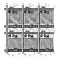
図4は画素領域全体のレイアウト図である。奇数行では、画素Aが左右方向に繰り返し配置され、偶数行では画素Bが左右方向に繰り返し配置されている。このようなレイアウトの液晶表示装置に対して、図5(a)のフレーム反転駆動方式の表示信号Vsigを印加する場合の動作について説明する。図5(a)の表示信号Vsigは1垂直期間(1V)毎に共通電位Vcomに対して極性が反転する。図4の1ライン目(第1行目)のゲートライン14のゲート信号がハイレベルになり、画素Aのトランジスタ1Aがオンする(薄膜トランジスタ1A,1BはNチャネル型とする)。
FIG. 4 is a layout diagram of the entire pixel region. In odd rows, pixels A are repeatedly arranged in the left-right direction, and in even rows, pixels B are repeatedly arranged in the left-right direction. The operation when the display signal Vsig of the frame inversion driving method of FIG. 5A is applied to the liquid crystal display device having such a layout will be described. The polarity of the display signal Vsig in FIG. 5A is inverted with respect to the common potential Vcom every vertical period (1V). The gate signal of the
すると、画素Aについて薄膜トランジスタ1Aを通して画素電極21Aに正極性の表示信号Vsigが印加されると、下層の画素電極21Aが上層の共通電極23Aに対して高電位になる。1水平期間(1H)かけて1ライン目の水平走査が行われると次に2ライン目(第2行目)のゲートライン14のゲート信号がハイレベルになり、画素Bのトランジスタ1Bがオンする。
Then, when a positive display signal Vsig is applied to the
すると、画素Bについて薄膜トランジスタ1Bを通して画素電極21Bに正極性の表示信号Vsigが印加されると、上層の画素電極21Bが下層の共通電極23Bに対して高電位になる。通常、低温ポリシリコンTFTの液晶ディスプレイではゲートライン14がハイレベルになり、TFTがオンしてから表示信号Vsigが印加される。それに対し、後述するアモルファスSi-TFT液晶ディスプレイでは表示信号Vsigが印加されてからゲートライン14がハイレベルになる。
Then, when a positive display signal Vsig is applied to the
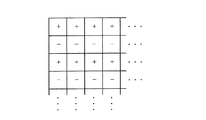
このようにして画素A、Bでは画素電極と共通電極の電位の関係は反転し、ライン反転駆動が行われることになる。図6において+、−記号は液晶に印加される電界の極性の正(+)、負(−)を表している。次のフレームでは表示信号Vsigの共通電位Vcomに対する極性が反転するので、図6において液晶に印加される電界の極性の正(+)、負(−)は反転する。 In this way, in the pixels A and B, the relationship between the potentials of the pixel electrode and the common electrode is inverted, and line inversion driving is performed. In FIG. 6, + and − symbols represent positive (+) and negative (−) polarities of the electric field applied to the liquid crystal. In the next frame, the polarity of the display signal Vsig with respect to the common potential Vcom is inverted, so that the positive (+) and negative (−) polarities of the electric field applied to the liquid crystal in FIG. 6 are inverted.
上述の液晶表示装置によれば、フレーム反転駆動を行うだけで画素領域ではライン反転駆動が行われることになる。これにより共通電極の信号歪による表示品位の低下が低減される。さらに従来のライン反転駆動と比較して共通電極に印加される信号の周波数が低くなることから周辺回路の低消費電力化が可能となる。 According to the above-described liquid crystal display device, line inversion driving is performed in the pixel region only by performing frame inversion driving. As a result, deterioration of display quality due to signal distortion of the common electrode is reduced. Further, since the frequency of the signal applied to the common electrode is lower than that of the conventional line inversion driving, the power consumption of the peripheral circuit can be reduced.
次に第2の実施の形態について図面を参照しながら説明する。この実施の形態は、第1の実施の形態において、共通電位ライン15を不要とするものである。図7に示すように、第1の行では第1層透明電極からなる画素電極21Aは画素毎に分離され、各薄膜トランジスタ1Aに接続されているが、第1の行の下の第2の行では、第1層透明電極からなる共通電極23Bは画素毎に分離されないで、一体化されている。そして、画素領域外において、この一体化された共通電極23BにVcom電位を供給する。
It will be described with reference to the drawings, a second embodiment in the following. In this embodiment, the common
また、図8に示すように、第1の行では第2層透明電極からなる共通電極23Aは画素毎に分離されないで、一体化されている。そして、共通電極23Aには共通電極23Bと同様に、画素領域外においてVcom電位を供給する。第2の行では、第2層透明電極からなる画素電極21Bは画素毎に分離され、各薄膜トランジスタ1Bに接続されている。
Further, as shown in FIG. 8, in the first row, the
したがって、図1、2の共通電位ライン15は不必要になることから画素の高開口率化が可能となり、表示品位が向上する。
Accordingly, since the common
次に第3の実施の形態について図面を参照しながら説明する。図9は、液晶表示装置の画素レイアウト図であり、図9(a)は第1層透明電極のレイアウトを示し、図9(b)は第1層透明電極のレイアウトに加えて、絶縁膜を介してその上に配置される第2層透明電極のレイアウトを示している。 Will be described with reference to the drawings third embodiment in the following. FIG. 9 is a pixel layout diagram of the liquid crystal display device. FIG. 9A shows the layout of the first transparent electrode, and FIG. 9B shows the insulating film in addition to the layout of the first transparent electrode. The layout of the 2nd layer transparent electrode arrange | positioned on it via is shown.
図9(a)に示すように、1つの行において、画素Aと画素Bが左右方向に交互に配置されている。このような構成によれば、隣接する画素A、Bの間で画素電極と共通電極の上下の配置関係が逆転される。図10は画素領域全体のレイアウト図である。各行で、画素A,画素Bが左右方向に交互に配置されているが、列方向(上下方向)では同じ画素A(または同じ画素B)が繰り返し配置されている。このようなレイアウトの液晶表示装置に対して、図11(a)のライン反転駆動方式の表示信号Vsigを印加する場合の動作について説明する。図11(a)の表示信号Vsigは1水平期間(1H)毎に、共通電位Vcomに対して極性が反転する。 As shown in FIG. 9A, the pixels A and B are alternately arranged in the left-right direction in one row. According to such a configuration, the vertical arrangement relationship of the pixel electrode and the common electrode is reversed between the adjacent pixels A and B. FIG. 10 is a layout diagram of the entire pixel region. In each row, the pixels A and B are alternately arranged in the left-right direction, but the same pixel A (or the same pixel B) is repeatedly arranged in the column direction (vertical direction). The operation when the display signal Vsig of the line inversion driving method of FIG. 11A is applied to the liquid crystal display device having such a layout will be described. The display signal Vsig in FIG. 11A is inverted in polarity with respect to the common potential Vcom every horizontal period ( 1 H).
図10の1ライン目のゲートライン14のゲート信号がハイレベルになり、画素A,Bの薄膜トランジスタ1A,1Bがオンする。(薄膜トランジスタ1A,1BはNチャネル型とする)すると、画素Aについて、薄膜トランジスタ1Aを通して画素電極21Aに正極性の表示信号Vsigが印加されると、下層の画素電極21Aが上層の共通電極23Aに対して高電位になる。画素Bについては、上層の画素電極21Bが下層の共通電極23Bに対して高電位となり、画素A,Bでは、画素電極と共通電極との間に生じる電界の向きが逆になる。
The gate signal of the
次に、1水平期間(1H)かけて1ライン目の水平走査が行われた後、2ライン目では表示信号Vsigの共通電位Vcomに対する極性が反転して水平走査が行われる。これによって、画素電極と共通電極の電位の関係は反転するが、画素A,Bでは、画素電極と共通電極との間の電界の向きが逆になる点は変わりない。このようにして、各ラインについてライン反転駆動が行われると、図12に示すようなドット反転駆動が行われることになる。図12において、+,−記号は液晶に印加される電界の極性の正(+)、負(−)を示している。 Next, after the horizontal scanning of the first line is performed over one horizontal period (1H), the polarity of the display signal Vsig with respect to the common potential Vcom is reversed and the horizontal scanning is performed on the second line. As a result, the relationship between the potentials of the pixel electrode and the common electrode is inverted, but the point that the direction of the electric field between the pixel electrode and the common electrode is reversed in the pixels A and B remains unchanged. In this way, when line inversion driving is performed for each line, dot inversion driving as shown in FIG. 12 is performed. In FIG. 12, + and − symbols indicate positive (+) and negative (−) polarity of the electric field applied to the liquid crystal.
したがって、上述の液晶表示装置によれば、ライン反転駆動を行うだけで、画素領域ではドット反転駆動が行われることになる。これにより、フリッカーを抑制することができるとともに、周辺回路の構成が簡単になり、消費電力も低減される。 Therefore, according to the above-described liquid crystal display device, dot inversion driving is performed in the pixel region only by performing line inversion driving. Accordingly, flicker can be suppressed, the configuration of the peripheral circuit is simplified, and power consumption is reduced.
次に第4の実施の形態について説明する。この実施の形態では、画素A,Bを用いる点は第1、2および3の実施の形態と同じであるが、画素A,Bの配置が異なっている。即ち、図13に示すように、1つの行において、画素A,Bは左右方向に交互に配置されているが、列方向(上下方向)にも交互に配置されている。すなわち、奇数行では、画素A,Bは左右方向に交互に配置され、偶数行では画素A,Bは逆の順番で左右方向に交互に配置されている。 A fourth embodiment will be described next. In this embodiment, the points using the pixels A and B are the same as those in the first, second and third embodiments, but the arrangement of the pixels A and B is different. That is, as shown in FIG. 13, in one row, the pixels A and B are alternately arranged in the left-right direction, but are also arranged alternately in the column direction (vertical direction). That is, in the odd rows, the pixels A and B are alternately arranged in the left-right direction, and in the even rows, the pixels A and B are alternately arranged in the left-right direction in the reverse order.
このような構成によれば、ライン反転駆動を行うことなく、図12のドット反転駆動が可能になる。この場合、画素電極に印加される表示信号Vsigは図5(a)のように、1垂直期間(1V)毎に、共通電位Vcomに対して反転された信号となる。したがって、本実施の形態によれば、ライン反転駆動を行うことなく、ドット反転駆動が行われることになるので、第3の実施の形態に比して、さらに周辺回路の構成が簡単になり、消費電力も低減される。 According to such a configuration, the dot inversion driving of FIG. 12 can be performed without performing the line inversion driving. In this case, the display signal Vsig applied to the pixel electrode is a signal inverted with respect to the common potential Vcom every one vertical period ( 1 V) as shown in FIG. Therefore, according to this embodiment, since dot inversion driving is performed without performing line inversion driving, the configuration of the peripheral circuit is further simplified as compared with the third embodiment, Power consumption is also reduced.
次に、第5の実施の形態について説明する。第1〜第4の実施の形態では、薄膜トランジスタは1A、1Bは低温ポリシリコンTFTであるが、本実施の形態ではその代わりに、アモルファスシリコンTFT(以下、aSi−TFTと略称する)が用いられる。この実施の形態は、第3の実施形態(図9参照)と同様の画素配列に対応しているが、第1、第2、第4の実施の形態についても同様に適用することができる。
Next , a fifth embodiment will be described. In the first to fourth embodiments, the
図14は、液晶表示装置の画素レイアウト図であり、図14(a)は第1層透明電極のレイアウトを示し、図14(b)は第1層透明電極のレイアウトに加えて、絶縁膜を介してその上に配置される第2層透明電極のレイアウトを示している。 14A and 14B are pixel layout diagrams of the liquid crystal display device. FIG. 14A shows a layout of the first transparent electrode, and FIG. 14B shows an insulating film in addition to the layout of the first transparent electrode. The layout of the 2nd layer transparent electrode arrange | positioned on it via is shown.
図14(a)に示すように、1つの行において、画素A’と画素B’が左右方向に交互に配置されている。画素A’については、第1層透明電極からなる画素電極121Aが形成され、コンタクトホールCH10を通してaSi−TFT11Aに接続されている。画素B’については、第1層透明電極で共通電極123Bが形成され、共通電位ライン115にオーバーラップして接続されている。
As shown in FIG. 14A, in one row, the pixels A ′ and the pixels B ′ are alternately arranged in the left-right direction. For the pixel A ′, a pixel electrode 121 </ b> A composed of a first layer transparent electrode is formed and connected to the aSi-
また、図14(b)に示すように、画素A’については、第2層透明電極からなる複数のスリットSA’を有する共通電極123Aが形成され、コンタクトホールCH11を通して共通電位ライン115に接続されている。画素B’については、第2層透明電極で複数のスリットSB’を有する画素電極121Bが形成され、コンタクトホールCH12を通してaSi−TFT11Bに接続されている。このような構成によれば、隣接する画素A’、B’の間で画素電極と共通電極の上下の配置関係が逆転される。
Further, as shown in FIG. 14B, for the pixel A ′, a
また、1つの行の中で、左右方向に延びるゲートライン114はaSi−TFT11A、11Bの共通のゲート電極である。このゲートライン114と交差して、上下方向に複数の表示信号ライン118が形成されており、対応する表示信号ライン118にaSi−TFT11A、11Bが接続されている。
In one row, a
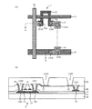
次に、画素A’の断面構造とその製造方法について図15を参照して説明する。まず、図15(a)に示すように、ガラス基板等からなるTFT基板100上に、クロム、モリブデン等からなるゲートライン114、共通電位ライン115が形成される。そして、ゲートライン114と共通電位ライン115との間のTFT基板100上に、第1層透明電極からなる画素電極121Aがパターニングされる。
Next, a cross-sectional structure of the pixel A ′ and a manufacturing method thereof will be described with reference to FIGS. First, as shown in FIG. 15A, a
次に、図15(b)に示すように、ゲートライン114及び共通電位ライン115を覆ってゲート絶縁膜101が形成される。ゲートライン114に近接した画素電極121A上のゲート絶縁膜101が部分的にエッチングされコンタクトホールCH10が形成される。
Next, as illustrated in FIG. 15B, the
次に、図15(c)に示すように、ゲートライン114を覆ってアモルファスシリコン層102が形成される。そして、アモルファスシリコン層102に接触して、アルミニウム等からなる表示信号ライン118(ドレイン電極)とソース電極103が形成される。ソース電極103はコンタクトホールCH10を通して画素電極121Aに接続される。
Next, as shown in FIG. 15C, the
次に、図15(d)に示すように、全面に層間絶縁膜104が形成される。そして、共通電位ライン115上のゲート絶縁膜101、層間絶縁膜104が部分的にエッチングされ、コンタクトホールCH11が形成される。次に、図15(e)に示すように、コンタクトホールCH11を通して共通電位ライン115に接続され、第2層透明電極からなる共通電極123Aが形成される。共通電極123Aはゲート絶縁膜101及び層間絶縁膜104を間に挟んで画素電極121A上に形成される。
Next, as shown in FIG. 15D, an
次に、画素B’の断面構造とその製造方法について図16を参照して説明する。まず、図16(a)に示すように、TFT基板100上にゲートライン114、共通電位ライン115が形成される。そして、共通電位ライン115を覆い、ゲートライン114と共通電位ライン115との間の領域に延びた共通電極123Bが形成される。共通電極123Bは共通電位ライン115に接触することで、それに接続される。
Next, a cross-sectional structure of the pixel B ′ and a manufacturing method thereof will be described with reference to FIGS. First, as shown in FIG. 16A, the
次に、図16(b)に示すように、全面にゲート絶縁膜101が形成される。次に、図16(c)に示すように、ゲートライン114を覆ってアモルファスシリコン層102が形成される。そして、アモルファスシリコン層102に接触して表示信号ライン118(ドレイン電極)とソース電極103が形成される。
Next, as shown in FIG. 16B, a
次に、図16(d)に示すように、全面に層間絶縁膜104が形成され、ソース電極103上の層間絶縁膜104が部分的にエッチングされ、コンタクトホールCH12が形成される。次に、図16(e)に示すように、コンタクトホールCH12を通してソース電極103に接続され、第2層透明電極からなる画素電極121Bが形成される。画素A’とは逆に、画素電極121Bはゲート絶縁膜101及び層間絶縁膜104を間に挟んで共通電極123B上に形成される。なお、TFT基板100と対向して対向基板が設けられ、TFT基板100と対向基板との間に液晶が封入されるなどの点については、第1〜第4の実施の形態と同様であるので詳細な説明は省略する。
Next, as shown in FIG. 16D, an
第1、第2、第3の実施の形態において、更に低消費電力化のために、図5(b)のように共通電位Vcomを1水平期間(1H)毎に反転する対極AC駆動としてもよい。また、第4の実施の形態において、図5(b)に示すように共通電位Vcomを1垂直期間(1V)毎に反転する対極AC駆動としてもよい。 In the first, second, and third embodiments, in order to further reduce power consumption, as shown in FIG. 5B, the common potential Vcom is inverted as a counter electrode AC drive that is inverted every horizontal period ( 1 H). Also good. Further, in the fourth embodiment, it may be the counter electrode AC driving which inverts the common potential Vcom every vertical period (1 V) as shown in Figure 5 (b).
1,1A,1B 薄膜トランジスタ 10,100 TFT基板
11 バッファ層 11A,11B aSi−TFT
12 能動層 12s ソース領域
12d ドレイン領域 13,101 ゲート絶縁膜
14,114 ゲートライン 15 共通電位ライン
16,104 層間絶縁膜 17,103 ソース電極
18,118 表示信号ライン 19 電極 20 平坦化膜
21,21A,21B,121,121A,121B 画素電極 22 絶縁膜
23,23A,23B,123,123A,123B 共通電極 30 対向基板
31,32 偏光板 40 液晶
102 アモルファスシリコン層 A,B,A’,B’ 画素
CH1〜CH12 コンタクトホール S,SA,SB,SA’,SB’ スリット
1,1A, 1B Thin film transistor 10,100
12
Claims (9)
前記第1の画素は第1の画素電極と、この第1の画素電極上に絶縁膜を介して配置され、複数の第1のスリットを有する第1の共通電極とを備え、
前記第2の画素は、第2の共通電極と、この第2の共通電極上に前記絶縁膜を介して配置され、複数の第2のスリットを有する第2の画素電極とを備え、
第1の行に、第1の画素を繰り返し配置し、第1の行に隣接した第2の行に、第2の画素を繰り返し配置し、前記第1の基板と、この第1の基板と対向する第2の基板の間に液晶を封入し、
前記第1の画素電極及び前記第2の共通電極が第1層透明電極からなり、前記第2の画素電極及び前記第1の共通電極が第2層透明電極からなる液晶表示装置。 A plurality of first pixels and second pixels on a first substrate;
The first pixel includes a first pixel electrode, and a first common electrode disposed on the first pixel electrode via an insulating film and having a plurality of first slits,
The second pixel includes a second common electrode, and a second pixel electrode disposed on the second common electrode via the insulating film and having a plurality of second slits.
The first pixel is repeatedly arranged in the first row, the second pixel is repeatedly arranged in the second row adjacent to the first row, the first substrate, the first substrate, Encapsulating liquid crystal between the opposing second substrates ,
The liquid crystal display device, wherein the first pixel electrode and the second common electrode are first layer transparent electrodes, and the second pixel electrode and the first common electrode are second layer transparent electrodes .
前記第1の画素は第1の画素電極と、この第1の画素電極上に絶縁膜を介して配置され、複数の第1のスリットを有する第1の共通電極とを備え、 The first pixel includes a first pixel electrode, and a first common electrode disposed on the first pixel electrode via an insulating film and having a plurality of first slits,
前記第2の画素は、第2の共通電極と、この第2の共通電極上に前記絶縁膜を介して配置され、複数の第2のスリットを有する第2の画素電極とを備え、 The second pixel includes a second common electrode, and a second pixel electrode disposed on the second common electrode via the insulating film and having a plurality of second slits.
第1の列に、第1の画素を繰り返し配置し、第1の列に隣接した第2の列に、第2の画素を繰り返し配置し、前記第1の基板と、この第1の基板と対向する第2の基板の間に液晶を封入し、 The first pixel is repeatedly arranged in the first column, the second pixel is repeatedly arranged in the second column adjacent to the first column, the first substrate, the first substrate, Encapsulating liquid crystal between the opposing second substrates,
前記第1の画素電極及び前記第2の共通電極が第1層透明電極からなり、前記第2の画素電極及び前記第1の共通電極が第2層透明電極からなる液晶表示装置。 The liquid crystal display device, wherein the first pixel electrode and the second common electrode are first layer transparent electrodes, and the second pixel electrode and the first common electrode are second layer transparent electrodes.
前記第1の画素は第1の画素電極と、この第1の画素電極上に絶縁膜を介して配置され、複数の第1のスリットを有する第1の共通電極とを備え、 The first pixel includes a first pixel electrode, and a first common electrode disposed on the first pixel electrode via an insulating film and having a plurality of first slits,
前記第2の画素は、第2の共通電極と、この第2の共通電極上に前記絶縁膜を介して配置され、複数の第2のスリットを有する第2の画素電極とを備え、 The second pixel includes a second common electrode, and a second pixel electrode disposed on the second common electrode via the insulating film and having a plurality of second slits.
第1の行に、第1の画素と第2の画素を交互に繰り返し配置し、第1の行に隣接した第2の行に、第1の画素と第2の画素を第1の行とは逆の順序で繰り返し配置し、前記第1の基板と、この第1の基板と対向する第2の基板の間に液晶を封入し、 The first pixel and the second pixel are alternately and repeatedly arranged in the first row, and the first pixel and the second pixel are arranged in the second row adjacent to the first row. Are repeatedly arranged in the reverse order, and the liquid crystal is sealed between the first substrate and the second substrate facing the first substrate,
前記第1の画素電極及び前記第2の共通電極が第1層透明電極からなり、前記第2の画素電極及び前記第1の共通電極が第2層透明電極からなる液晶表示装置。 The liquid crystal display device, wherein the first pixel electrode and the second common electrode are first layer transparent electrodes, and the second pixel electrode and the first common electrode are second layer transparent electrodes.
Priority Applications (2)
| Application Number | Priority Date | Filing Date | Title |
|---|---|---|---|
| JP2006085953A JP4797740B2 (en) | 2006-03-27 | 2006-03-27 | Liquid crystal display |
| US11/727,146 US7889303B2 (en) | 2006-03-27 | 2007-03-23 | Liquid crystal display device |
Applications Claiming Priority (1)
| Application Number | Priority Date | Filing Date | Title |
|---|---|---|---|
| JP2006085953A JP4797740B2 (en) | 2006-03-27 | 2006-03-27 | Liquid crystal display |
Publications (3)
| Publication Number | Publication Date |
|---|---|
| JP2007264080A JP2007264080A (en) | 2007-10-11 |
| JP2007264080A5 JP2007264080A5 (en) | 2008-04-03 |
| JP4797740B2 true JP4797740B2 (en) | 2011-10-19 |
Family
ID=38532978
Family Applications (1)
| Application Number | Title | Priority Date | Filing Date |
|---|---|---|---|
| JP2006085953A Active JP4797740B2 (en) | 2006-03-27 | 2006-03-27 | Liquid crystal display |
Country Status (2)
| Country | Link |
|---|---|
| US (1) | US7889303B2 (en) |
| JP (1) | JP4797740B2 (en) |
Families Citing this family (31)
| Publication number | Priority date | Publication date | Assignee | Title |
|---|---|---|---|---|
| JP4952425B2 (en) * | 2006-08-21 | 2012-06-13 | ソニー株式会社 | Liquid crystal device and electronic device |
| TW200815859A (en) * | 2006-09-19 | 2008-04-01 | Epson Imaging Devices Corp | Liquid crystal display device |
| US8351006B2 (en) * | 2007-05-14 | 2013-01-08 | Lg Display Co., Ltd. | Liquid crystal display device and fabricating method thereof |
| JP5107653B2 (en) * | 2007-10-09 | 2012-12-26 | 株式会社ジャパンディスプレイイースト | Liquid crystal display |
| US7847905B2 (en) * | 2007-11-07 | 2010-12-07 | Hydis Technologies Co., Ltd. | FFS mode LCD and method of manufacturing the same |
| JP5079463B2 (en) * | 2007-11-20 | 2012-11-21 | 株式会社ジャパンディスプレイウェスト | Liquid crystal display device and manufacturing method thereof |
| JP2010060967A (en) * | 2008-09-05 | 2010-03-18 | Epson Imaging Devices Corp | Liquid crystal display device and electronic apparatus |
| US8552957B2 (en) * | 2009-02-02 | 2013-10-08 | Apple Inc. | Liquid crystal display reordered inversion |
| JP5500712B2 (en) * | 2009-09-02 | 2014-05-21 | 株式会社ジャパンディスプレイ | LCD panel |
| JP4911793B2 (en) | 2009-11-09 | 2012-04-04 | 東芝モバイルディスプレイ株式会社 | Liquid crystal display |
| CN102156359B (en) * | 2010-06-13 | 2014-05-07 | 京东方科技集团股份有限公司 | Array base plate, liquid crystal panel, liquid crystal display and driving method |
| KR101866946B1 (en) | 2010-11-02 | 2018-06-14 | 삼성디스플레이 주식회사 | Thin film transistor array panel and the method for manufacturing thereof |
| CN102129143A (en) * | 2010-12-15 | 2011-07-20 | 华映视讯(吴江)有限公司 | Pixel array substrate and manufacturing method thereof |
| WO2012128061A1 (en) * | 2011-03-18 | 2012-09-27 | シャープ株式会社 | Liquid crystal drive method and liquid crystal display device |
| CN103430088A (en) | 2011-03-25 | 2013-12-04 | 夏普株式会社 | Display device |
| US8953132B2 (en) | 2011-03-30 | 2015-02-10 | Au Optronics Corp. | Pixel array of fringe field switching liquid crystal display panel and driving method thereof |
| CN102207656A (en) * | 2011-03-30 | 2011-10-05 | 友达光电股份有限公司 | Pixel array of fringe field switching liquid crystal display panel and driving method thereof |
| TWI446077B (en) * | 2011-08-17 | 2014-07-21 | Chunghwa Picture Tubes Ltd | Pixel structure of fringe field switching mode lcd |
| TWI442152B (en) * | 2011-10-06 | 2014-06-21 | Hannstar Display Corp | Display devices and fabrication methods thereof |
| JP5917127B2 (en) | 2011-12-19 | 2016-05-11 | 株式会社ジャパンディスプレイ | Liquid crystal display |
| CN102654988A (en) * | 2012-03-23 | 2012-09-05 | 京东方科技集团股份有限公司 | Liquid crystal display drive circuit, liquid crystal display zone and drive method of liquid crystal display |
| KR101295536B1 (en) | 2012-03-26 | 2013-08-12 | 엘지디스플레이 주식회사 | Display device with integrated touch screen and method for manufacturing the same |
| CN102810304B (en) * | 2012-08-09 | 2015-02-18 | 京东方科技集团股份有限公司 | Pixel unit, pixel structure, display device and pixel driving method |
| JP2014174402A (en) * | 2013-03-11 | 2014-09-22 | Japan Display Inc | Liquid crystal display device |
| JP6207264B2 (en) * | 2013-07-03 | 2017-10-04 | 三菱電機株式会社 | Liquid crystal display |
| JP5681822B2 (en) * | 2014-03-10 | 2015-03-11 | 株式会社ジャパンディスプレイ | LCD panel |
| CN104992926B (en) * | 2015-07-24 | 2018-03-13 | 深圳市华星光电技术有限公司 | LTPS array base paltes and its manufacture method |
| CN106873267B (en) * | 2015-12-14 | 2021-02-19 | 群创光电股份有限公司 | Display panel |
| TWI595298B (en) * | 2015-12-14 | 2017-08-11 | 群創光電股份有限公司 | Display panel |
| JP6723080B2 (en) | 2016-06-08 | 2020-07-15 | 三菱電機株式会社 | Liquid crystal display |
| CN105974693A (en) * | 2016-07-27 | 2016-09-28 | 京东方科技集团股份有限公司 | Array substrate, display panel, display device and driving method |
Family Cites Families (7)
| Publication number | Priority date | Publication date | Assignee | Title |
|---|---|---|---|---|
| KR100311214B1 (en) * | 1999-06-29 | 2001-11-02 | 박종섭 | LCD having high aperture ratio and high transmittance |
| KR100520381B1 (en) * | 2000-05-31 | 2005-10-11 | 비오이 하이디스 테크놀로지 주식회사 | Fringe field switching mode lcd device |
| JP3668844B2 (en) * | 2000-10-04 | 2005-07-06 | 松下電器産業株式会社 | Display device and driving method thereof |
| KR100482468B1 (en) * | 2000-10-10 | 2005-04-14 | 비오이 하이디스 테크놀로지 주식회사 | Fringe field switching mode lcd |
| KR100381868B1 (en) * | 2000-11-29 | 2003-05-01 | 삼성전자주식회사 | a liquid crystal display and a substrate for the same |
| JP4556341B2 (en) | 2001-03-30 | 2010-10-06 | セイコーエプソン株式会社 | Liquid crystal display device and electronic device |
| TW544940B (en) * | 2002-07-03 | 2003-08-01 | Au Optronics Corp | Thin film transistor array |
-
2006
- 2006-03-27 JP JP2006085953A patent/JP4797740B2/en active Active
-
2007
- 2007-03-23 US US11/727,146 patent/US7889303B2/en active Active
Also Published As
| Publication number | Publication date |
|---|---|
| US20070222907A1 (en) | 2007-09-27 |
| US7889303B2 (en) | 2011-02-15 |
| JP2007264080A (en) | 2007-10-11 |
Similar Documents
| Publication | Publication Date | Title |
|---|---|---|
| JP4797740B2 (en) | Liquid crystal display | |
| JP4449953B2 (en) | Liquid crystal display | |
| KR101171414B1 (en) | Liquid crystal display device | |
| US8134155B2 (en) | Liquid crystal display device capable of reducing leakage current, and fabrication method thereof | |
| JP5638833B2 (en) | Image display device and manufacturing method thereof | |
| US8736781B2 (en) | Liquid crystal display device and method of driving the same | |
| JP2018063348A (en) | Liquid crystal display panel and liquid crystal display device | |
| JP2007156392A (en) | Liquid crystal panel | |
| JP2007293155A (en) | Liquid crystal display device | |
| JP4367506B2 (en) | Electro-optical device driving method, electro-optical device, and electronic apparatus | |
| JP2010002504A (en) | Liquid crystal display device | |
| JP2010026237A (en) | Liquid crystal display | |
| US8542327B2 (en) | Liquid crystal display device | |
| JP4187027B2 (en) | Display device | |
| JP2007128094A (en) | Display substrate and liquid crystal display panel and display device having the same | |
| KR20040061786A (en) | Method for fabricating for an array substrate for In-Plane switching mode LCD | |
| JPH1010556A (en) | Liquid crystal display device | |
| KR102129500B1 (en) | Liquid crystal display panel | |
| JP5072530B2 (en) | Liquid crystal device and electronic device including the same | |
| JP4501979B2 (en) | Liquid crystal display | |
| KR20090058989A (en) | Thin film transistor and method of fabricating the same | |
| KR101227133B1 (en) | Liquid Crystal Display Panel Of Horizontal Electronic Fileld Applying Type | |
| JP2004101615A (en) | Active matrix substrate, liquid crystal device, electronic apparatus | |
| JP7092914B2 (en) | Display device | |
| JP2007094147A (en) | Display device and manufacturing method thereof |
Legal Events
| Date | Code | Title | Description |
|---|---|---|---|
| A521 | Request for written amendment filed |
Free format text: JAPANESE INTERMEDIATE CODE: A523 Effective date: 20080219 |
|
| A621 | Written request for application examination |
Free format text: JAPANESE INTERMEDIATE CODE: A621 Effective date: 20080219 |
|
| A711 | Notification of change in applicant |
Free format text: JAPANESE INTERMEDIATE CODE: A711 Effective date: 20100526 |
|
| RD02 | Notification of acceptance of power of attorney |
Free format text: JAPANESE INTERMEDIATE CODE: A7422 Effective date: 20100526 |
|
| A977 | Report on retrieval |
Free format text: JAPANESE INTERMEDIATE CODE: A971007 Effective date: 20110214 |
|
| A131 | Notification of reasons for refusal |
Free format text: JAPANESE INTERMEDIATE CODE: A131 Effective date: 20110222 |
|
| A521 | Request for written amendment filed |
Free format text: JAPANESE INTERMEDIATE CODE: A523 Effective date: 20110407 |
|
| TRDD | Decision of grant or rejection written | ||
| A01 | Written decision to grant a patent or to grant a registration (utility model) |
Free format text: JAPANESE INTERMEDIATE CODE: A01 Effective date: 20110705 |
|
| A01 | Written decision to grant a patent or to grant a registration (utility model) |
Free format text: JAPANESE INTERMEDIATE CODE: A01 |
|
| A61 | First payment of annual fees (during grant procedure) |
Free format text: JAPANESE INTERMEDIATE CODE: A61 Effective date: 20110718 |
|
| FPAY | Renewal fee payment (event date is renewal date of database) |
Free format text: PAYMENT UNTIL: 20140812 Year of fee payment: 3 |
|
| R151 | Written notification of patent or utility model registration |
Ref document number: 4797740 Country of ref document: JP Free format text: JAPANESE INTERMEDIATE CODE: R151 |
|
| FPAY | Renewal fee payment (event date is renewal date of database) |
Free format text: PAYMENT UNTIL: 20140812 Year of fee payment: 3 |
|
| FPAY | Renewal fee payment (event date is renewal date of database) |
Free format text: PAYMENT UNTIL: 20140812 Year of fee payment: 3 |
|
| S111 | Request for change of ownership or part of ownership |
Free format text: JAPANESE INTERMEDIATE CODE: R313113 |
|
| FPAY | Renewal fee payment (event date is renewal date of database) |
Free format text: PAYMENT UNTIL: 20140812 Year of fee payment: 3 |
|
| R350 | Written notification of registration of transfer |
Free format text: JAPANESE INTERMEDIATE CODE: R350 |
|
| R250 | Receipt of annual fees |
Free format text: JAPANESE INTERMEDIATE CODE: R250 |
|
| R250 | Receipt of annual fees |
Free format text: JAPANESE INTERMEDIATE CODE: R250 |
|
| R250 | Receipt of annual fees |
Free format text: JAPANESE INTERMEDIATE CODE: R250 |
|
| R250 | Receipt of annual fees |
Free format text: JAPANESE INTERMEDIATE CODE: R250 |
|
| R250 | Receipt of annual fees |
Free format text: JAPANESE INTERMEDIATE CODE: R250 |
|
| R250 | Receipt of annual fees |
Free format text: JAPANESE INTERMEDIATE CODE: R250 |
|
| R250 | Receipt of annual fees |
Free format text: JAPANESE INTERMEDIATE CODE: R250 |
|
| S111 | Request for change of ownership or part of ownership |
Free format text: JAPANESE INTERMEDIATE CODE: R313111 |
|
| R350 | Written notification of registration of transfer |
Free format text: JAPANESE INTERMEDIATE CODE: R350 |
|
| R250 | Receipt of annual fees |
Free format text: JAPANESE INTERMEDIATE CODE: R250 |
|
| R250 | Receipt of annual fees |
Free format text: JAPANESE INTERMEDIATE CODE: R250 |
|
| R250 | Receipt of annual fees |
Free format text: JAPANESE INTERMEDIATE CODE: R250 |