JP2010026237A - Liquid crystal display - Google Patents
Liquid crystal display Download PDFInfo
- Publication number
- JP2010026237A JP2010026237A JP2008187245A JP2008187245A JP2010026237A JP 2010026237 A JP2010026237 A JP 2010026237A JP 2008187245 A JP2008187245 A JP 2008187245A JP 2008187245 A JP2008187245 A JP 2008187245A JP 2010026237 A JP2010026237 A JP 2010026237A
- Authority
- JP
- Japan
- Prior art keywords
- electrode
- liquid crystal
- crystal display
- display device
- insulating film
- Prior art date
- Legal status (The legal status is an assumption and is not a legal conclusion. Google has not performed a legal analysis and makes no representation as to the accuracy of the status listed.)
- Granted
Links
- 239000004973 liquid crystal related substance Substances 0.000 title claims abstract description 203
- 239000000758 substrate Substances 0.000 claims abstract description 88
- 230000005684 electric field Effects 0.000 claims abstract description 12
- 239000011159 matrix material Substances 0.000 claims abstract description 8
- 239000010410 layer Substances 0.000 claims description 128
- 239000010409 thin film Substances 0.000 claims description 65
- 239000010408 film Substances 0.000 description 249
- 239000003990 capacitor Substances 0.000 description 58
- 238000000034 method Methods 0.000 description 44
- 102100036464 Activated RNA polymerase II transcriptional coactivator p15 Human genes 0.000 description 38
- 101000713904 Homo sapiens Activated RNA polymerase II transcriptional coactivator p15 Proteins 0.000 description 38
- 229910004444 SUB1 Inorganic materials 0.000 description 38
- 230000001681 protective effect Effects 0.000 description 35
- 239000011521 glass Substances 0.000 description 34
- 238000004519 manufacturing process Methods 0.000 description 20
- 230000015572 biosynthetic process Effects 0.000 description 18
- 239000004065 semiconductor Substances 0.000 description 12
- 238000010586 diagram Methods 0.000 description 11
- 239000007772 electrode material Substances 0.000 description 10
- 238000005530 etching Methods 0.000 description 10
- 229910052581 Si3N4 Inorganic materials 0.000 description 8
- 239000002585 base Substances 0.000 description 8
- 230000000694 effects Effects 0.000 description 8
- HQVNEWCFYHHQES-UHFFFAOYSA-N silicon nitride Chemical compound N12[Si]34N5[Si]62N3[Si]51N64 HQVNEWCFYHHQES-UHFFFAOYSA-N 0.000 description 8
- 229910021417 amorphous silicon Inorganic materials 0.000 description 6
- 229910010272 inorganic material Inorganic materials 0.000 description 6
- 239000011147 inorganic material Substances 0.000 description 6
- NIXOWILDQLNWCW-UHFFFAOYSA-N acrylic acid group Chemical group C(C=C)(=O)O NIXOWILDQLNWCW-UHFFFAOYSA-N 0.000 description 5
- 238000010438 heat treatment Methods 0.000 description 5
- 238000000206 photolithography Methods 0.000 description 5
- 238000004528 spin coating Methods 0.000 description 5
- 239000011248 coating agent Substances 0.000 description 4
- 238000000576 coating method Methods 0.000 description 4
- 101150037603 cst-1 gene Proteins 0.000 description 4
- 229910004438 SUB2 Inorganic materials 0.000 description 3
- 101100311330 Schizosaccharomyces pombe (strain 972 / ATCC 24843) uap56 gene Proteins 0.000 description 3
- 101150018444 sub2 gene Proteins 0.000 description 3
- VYPSYNLAJGMNEJ-UHFFFAOYSA-N Silicium dioxide Chemical compound O=[Si]=O VYPSYNLAJGMNEJ-UHFFFAOYSA-N 0.000 description 2
- 239000003513 alkali Substances 0.000 description 2
- FFBHFFJDDLITSX-UHFFFAOYSA-N benzyl N-[2-hydroxy-4-(3-oxomorpholin-4-yl)phenyl]carbamate Chemical class OC1=C(NC(=O)OCC2=CC=CC=C2)C=CC(=C1)N1CCOCC1=O FFBHFFJDDLITSX-UHFFFAOYSA-N 0.000 description 2
- 230000002950 deficient Effects 0.000 description 2
- 238000009413 insulation Methods 0.000 description 2
- 230000014759 maintenance of location Effects 0.000 description 2
- OSDXSOSJRPQCHJ-XVNBXDOJSA-N methyl 3-(3,4-dihydroxyphenyl)-3-[(E)-3-(3,4-dihydroxyphenyl)prop-2-enoyl]oxypropanoate Chemical compound C=1C=C(O)C(O)=CC=1C(CC(=O)OC)OC(=O)\C=C\C1=CC=C(O)C(O)=C1 OSDXSOSJRPQCHJ-XVNBXDOJSA-N 0.000 description 2
- AMGQUBHHOARCQH-UHFFFAOYSA-N indium;oxotin Chemical compound [In].[Sn]=O AMGQUBHHOARCQH-UHFFFAOYSA-N 0.000 description 1
- 239000011229 interlayer Substances 0.000 description 1
- 239000000203 mixture Substances 0.000 description 1
- 239000011368 organic material Substances 0.000 description 1
- 230000001151 other effect Effects 0.000 description 1
- 230000002093 peripheral effect Effects 0.000 description 1
- 229910021420 polycrystalline silicon Inorganic materials 0.000 description 1
- 229920005591 polysilicon Polymers 0.000 description 1
Images


Abstract
Description
本発明は液晶表示装置に関し、特に保持容量を画素電極と対向電極とで構成した液晶表示装置に関する。 The present invention relates to a liquid crystal display device, and more particularly to a liquid crystal display device in which a storage capacitor is constituted by a pixel electrode and a counter electrode.
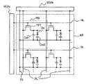
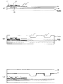
従来の液晶表示装置は、画素電極等が形成される図2に示す第1基板と、この第1基板に対向して配置される第2基板と、第1基板と第2基板とで挟持される液晶層とで構成されている。 A conventional liquid crystal display device is sandwiched between a first substrate shown in FIG. 2 on which pixel electrodes and the like are formed, a second substrate disposed opposite to the first substrate, and the first substrate and the second substrate. And a liquid crystal layer.
図2に示すように構成された従来の液晶表示装置では、薄膜トランジスタTFTのゲート電極GTにはゲート線GLから信号が入力される構成となっており、ドレイン電極DTにはドレイン線DLからの信号が入力される構成となっている。一方、薄膜トランジスタTFTのソースには液晶層に表示データに対応した電界を印加するための画素電極PXが設けられており、この画素電極PXに供給された電荷を1フレーム期間保持するための保持容量Cst1が画素電極PXと対向電極CT間に設けられている。また、画素電極PXと対向電極CTとの間には液晶層を介在させることによる液晶容量Clcと絶縁膜容量Cst2とが直列に形成される構成となっている。 In the conventional liquid crystal display device configured as shown in FIG. 2, a signal is input from the gate line GL to the gate electrode GT of the thin film transistor TFT, and a signal from the drain line DL is input to the drain electrode DT. Is input. On the other hand, the source of the thin film transistor TFT is provided with a pixel electrode PX for applying an electric field corresponding to display data to the liquid crystal layer, and a storage capacitor for holding the charge supplied to the pixel electrode PX for one frame period. Cst1 is provided between the pixel electrode PX and the counter electrode CT. In addition, a liquid crystal capacitor Clc and an insulating film capacitor Cst2 are formed in series by interposing a liquid crystal layer between the pixel electrode PX and the counter electrode CT.
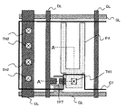
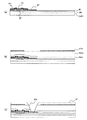
以下、図3に従来の液晶表示装置の1画素分の液晶表示素子の平面図を示し、図4に図3中のA−A'線での断面図を示し、図3及び図4に基づいて絶縁膜容量について説明する。 3 is a plan view of a liquid crystal display element for one pixel of a conventional liquid crystal display device, FIG. 4 is a sectional view taken along line AA ′ in FIG. 3, and is based on FIGS. The insulating film capacitance will be described.
図3及び図4に示すように、従来の液晶表示装置は対向電極CTの上層に形成した容量絶縁膜CIを介して画素電極PXが配置される構成となっている。このように形成される従来の液晶表示装置では、保持容量を構成するための一対の電極を画素電極PXと対向電極CTとで兼ねる構成とすることが一般的に行われている。すなわち、画素電極PXと対向電極CTとの間に形成する層間絶縁膜として容量絶縁膜CIを用いることにより、画素電極PXと対向電極CTとの絶縁を実現しつつ画素電極PXと対向電極CTとで画素電荷の保持に必要な保持容量を実現する構成となっている。 As shown in FIGS. 3 and 4, the conventional liquid crystal display device has a configuration in which the pixel electrode PX is arranged via a capacitive insulating film CI formed in the upper layer of the counter electrode CT. In the conventional liquid crystal display device formed in this way, it is generally performed that the pair of electrodes for constituting the storage capacitor is also used as the pixel electrode PX and the counter electrode CT. That is, by using the capacitor insulating film CI as an interlayer insulating film formed between the pixel electrode PX and the counter electrode CT, the pixel electrode PX and the counter electrode CT can be insulated while realizing the insulation between the pixel electrode PX and the counter electrode CT. Thus, the storage capacitance necessary for holding the pixel charge is realized.
このような従来の液晶表示装置では、容量絶縁膜CIの内部または液晶層と容量絶縁膜CIとの界面に存在する固定電荷すなわち絶縁膜容量Cst2に蓄えられる電荷により、交流反転駆動の際の振幅が正極性の時と負極正の時で異なり、フリッカが発生してしまうことが知られている。 In such a conventional liquid crystal display device, the amplitude at the time of AC inversion driving is caused by fixed charges existing inside the capacitive insulating film CI or at the interface between the liquid crystal layer and the capacitive insulating film CI, that is, charges accumulated in the insulating film capacitance Cst2. It is known that flicker occurs when the positive polarity is different from the positive polarity and negative polarity.
この問題を解決する技術として、特許文献1に記載の液晶表示装置がある。特許文献1に記載の液晶表示装置では、対向電極の上層に絶縁膜を形成した後に、絶縁膜の形状を画素電極形状にエッチング加工し、画素電極を形成する構成となっている。
従来の液晶表示装置では液晶層に印加する電界強度の低下を最小限にするために、薄膜トランジスタの上層に無機材料の保護絶縁膜を形成し、その上層に有機材料の平坦化膜を形成した後、平坦化膜の上層に液晶層を駆動するための対向電極や画素電極を形成する構成となっている。 In the conventional liquid crystal display device, in order to minimize the decrease in the electric field strength applied to the liquid crystal layer, an inorganic material protective insulating film is formed on the upper layer of the thin film transistor, and an organic material planarizing film is formed on the upper layer. The counter electrode and the pixel electrode for driving the liquid crystal layer are formed on the planarizing film.
しかしながら、特許文献1に記載の技術では、櫛歯状に形成した画素電極の形状に絶縁膜を加工する、すなわち櫛歯形状の画素電極の開口部の絶縁膜を除去する構成となっている。 However, the technique described in Patent Document 1 has a configuration in which an insulating film is processed into the shape of a comb-shaped pixel electrode, that is, the insulating film at the opening of the comb-shaped pixel electrode is removed.
このために、特許文献1に記載の技術では、画素電極の開口部の段差が大きくなってしまうので、画素電極の上層に形成されるラビング層を形成する際にラビング不良が発生し、液晶表示装置のコントラストが低下してしまうという問題があった。 For this reason, in the technique described in Patent Document 1, a step difference in the opening of the pixel electrode becomes large, and thus a rubbing failure occurs when a rubbing layer formed on the upper layer of the pixel electrode is formed. There is a problem that the contrast of the apparatus is lowered.
本発明の目的は、フリッカを低減することが可能な液晶表示装置を提供することにある。 An object of the present invention is to provide a liquid crystal display device capable of reducing flicker.
本発明の他の目的は、ラビング不良によるコントラストの低下を抑制することが可能な液晶表示装置を提供することにある。 Another object of the present invention is to provide a liquid crystal display device capable of suppressing a decrease in contrast due to defective rubbing.
前記課題を解決すべく、本願発明は、例えば、下記のように構成される。 In order to solve the above problems, the present invention is configured as follows, for example.
(1)本願発明の液晶表示装置は、マトリックス状に複数の画素が配置され、液晶層を介して対向配置される第1及び第2の基板と、前記第1の基板側に、少なくとも各画素内に面状に形成された第1電極と、前記第1電極の上層に第1絶縁層を介して形成され、各画素毎に前記第1電極に重畳して形成される線状の複数の第2電極とを有し、前記第1電極と前記第2電極で生じる電界で前記液晶層を駆動する液晶表示装置であって、前記第1電極と同電位であり、前記第2電極と同層に形成され、前記各第2電極を間にして配置される線状の第3電極を備えたものである。 (1) In the liquid crystal display device of the present invention, a plurality of pixels are arranged in a matrix, and at least each pixel is disposed on the first and second substrates opposed to each other with a liquid crystal layer interposed therebetween. A first electrode formed in a planar shape inside, and a plurality of linear electrodes formed on the first electrode via a first insulating layer and superimposed on the first electrode for each pixel. A liquid crystal display device having a second electrode and driving the liquid crystal layer with an electric field generated by the first electrode and the second electrode, the liquid crystal display device having the same potential as the first electrode, and the same as the second electrode It is provided with a linear third electrode which is formed in a layer and arranged with the second electrodes interposed therebetween.
(2)(1)に記載の液晶表示装置において、前記第1電極と前記第3電極とが一体に形成された導電層からなるものである。 (2) In the liquid crystal display device according to (1), the first electrode and the third electrode are formed of a conductive layer integrally formed.
(3)(1)又は(2)に記載の液晶表示装置において、平坦化層に溝が形成され、前記溝に前記第1電極の一部が形成されるものである。 (3) In the liquid crystal display device according to (1) or (2), a groove is formed in the planarization layer, and a part of the first electrode is formed in the groove.
(4)(1)又は(2)に記載の液晶表示装置において、平坦化層の上層に形成された第2絶縁層を有し、前記第2絶縁層に形成された溝に前記第1電極の一部が形成されているものである。 (4) In the liquid crystal display device according to (1) or (2), the liquid crystal display device has a second insulating layer formed in an upper layer of a planarizing layer, and the first electrode is formed in a groove formed in the second insulating layer. Is formed.
(5)(1)に記載の液晶表示装置において、前記第1電極と前記第3電極とが前記第1絶縁層に形成されたコンタクト部を介して接続されるものである。 (5) In the liquid crystal display device according to (1), the first electrode and the third electrode are connected through a contact portion formed in the first insulating layer.
(6)(1)又は(5)に記載の液晶表示装置において、前記第1絶縁層が容量絶縁層で形成され、前記第2電極と前記第3電極とが前記第1絶縁層上に形成されるものである。 (6) In the liquid crystal display device according to (1) or (5), the first insulating layer is formed of a capacitive insulating layer, and the second electrode and the third electrode are formed on the first insulating layer. It is what is done.
(7)(1)乃至(7)のいずれかに記載の液晶表示装置において、前記第2電極に表示用の電荷を入力する薄膜トランジスタを有し、前記薄膜トランジスタのソース電極と前記第2電極とを接続するコンタクト部を前記第1絶縁層で平坦化したものである。 (7) In the liquid crystal display device according to any one of (1) to (7), the liquid crystal display device includes a thin film transistor that inputs display charges to the second electrode, and the source electrode and the second electrode of the thin film transistor are provided. The contact portion to be connected is flattened with the first insulating layer.
本発明の液晶表示装置では、対向電極と同電位であり、画素電極と同層に形成され、該画素電極を間にして配置される線状の第3電極を備える構成となっているので、液晶層と絶縁層との間に生じる容量を大幅に低減でき、フリッカを低減することができる。 In the liquid crystal display device of the present invention, it has the same potential as the counter electrode, is formed in the same layer as the pixel electrode, and includes a linear third electrode disposed with the pixel electrode in between. The capacitance generated between the liquid crystal layer and the insulating layer can be greatly reduced, and flicker can be reduced.
また、各画素毎に画素電極と同一層上に形成される第3電極を備える構成となっているので、画素電極の上層に形成するラビング層の不良発生を防止し、液晶表示装置のコントラスト低下を防止することができる。 In addition, since each pixel has a third electrode formed on the same layer as the pixel electrode, it is possible to prevent a rubbing layer formed on the upper layer of the pixel electrode from being defective and to reduce the contrast of the liquid crystal display device. Can be prevented.
本発明のその他の効果については、明細書全体の記載から明らかにされる。 Other effects of the present invention will become apparent from the description of the entire specification.
以下、本発明が適用された実施形態の例について、図面を用いて説明する。なお、下記では、液晶表示装置の構成を、その製造工程により説明する場合もある。ただし、以下の説明において、同一構成要素には同一符号を付し繰り返しの説明は省略する。 Hereinafter, an example of an embodiment to which the present invention is applied will be described with reference to the drawings. In the following description, the structure of the liquid crystal display device may be described by its manufacturing process. However, in the following description, the same components are denoted by the same reference numerals, and repeated description is omitted.
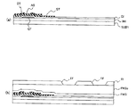
(実施形態1)
図5は本発明の実施形態1の液晶表示装置の概略構成図であり、図6は図3に示す実施形態1の液晶表示装置の1画素分の液晶表示素子の平面図であり、図1は図6に示すB−B'線での断面図である。なお、薄膜トランジスタとしてアモルファスシリコンTFTの場合について説明するが、これに限定されることはなくポリシリコンTFTを用いてもよい。また、スイッチング素子として薄膜トランジスタの代わりにダイオード等を用いてもよい。
(Embodiment 1)
5 is a schematic configuration diagram of the liquid crystal display device according to the first embodiment of the present invention, and FIG. 6 is a plan view of a liquid crystal display element for one pixel of the liquid crystal display device according to the first embodiment shown in FIG. FIG. 7 is a cross-sectional view taken along line BB ′ shown in FIG. 6. Although the case of an amorphous silicon TFT is described as the thin film transistor, the present invention is not limited to this, and a polysilicon TFT may be used. A diode or the like may be used as the switching element instead of the thin film transistor.
実施形態1の液晶表示装置は、後述するように画素電極等が形成される第1基板と、この第1基板に対向して配置される第2基板と、第1基板と第2基板とで挟持される液晶層とで構成されている。 The liquid crystal display device of Embodiment 1 includes a first substrate on which pixel electrodes and the like are formed, a second substrate disposed opposite to the first substrate, a first substrate, and a second substrate, as will be described later. It is comprised with the liquid crystal layer pinched | interposed.
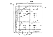
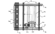
図5に示すように、実施形態1の液晶表示装置の第1基板にはゲート線GLが横方向に多数配置され、ドレイン線DLが縦方向に多数配置される構成となっている。各ゲート線GLと各ドレイン線DLとのそれぞれの交点には、薄膜トランジスタTFTと画素容量とからなる画素が形成されている。また、各画素の対向電極には共通電圧(コモン電圧)を供給するためのコモン線CLがドレイン線DLと平行に構成されている。ゲート線GLにはゲートドライバSCDvからの画素選択のためのゲート信号が供給され、ドレイン線にはドレインドライバSCDhから各画素への書き込み電圧であるドレイン信号が供給される構成となっている。コモン線CLには図示しないコモンドライバから液晶表示装置の駆動形式に応じたコモン信号(基準信号(電圧))が供給される構成となっている。ただし、隣接する一対のゲート線GLと隣接する一対のドレイン線DLで囲まれる矩形状の領域は画素が形成される領域を構成し、この各画素は液晶表示領域AR内においてマトリックス状に配置される。 As shown in FIG. 5, the first substrate of the liquid crystal display device of Embodiment 1 has a configuration in which a large number of gate lines GL are arranged in the horizontal direction and a large number of drain lines DL are arranged in the vertical direction. A pixel composed of a thin film transistor TFT and a pixel capacitor is formed at each intersection of each gate line GL and each drain line DL. Further, a common line CL for supplying a common voltage (common voltage) to the counter electrode of each pixel is configured in parallel with the drain line DL. A gate signal for pixel selection from the gate driver SCDv is supplied to the gate line GL, and a drain signal that is a write voltage to each pixel is supplied from the drain driver SCDh to the drain line. The common line CL is configured to be supplied with a common signal (reference signal (voltage)) corresponding to the driving format of the liquid crystal display device from a common driver (not shown). However, a rectangular region surrounded by a pair of adjacent gate lines GL and a pair of adjacent drain lines DL constitutes a region where pixels are formed, and these pixels are arranged in a matrix in the liquid crystal display region AR. The
このように構成された実施形態1の液晶表示装置における第1基板では、薄膜トランジスタTFTのゲート電極GTにはゲート線GLからゲート信号(走査信号(電圧))が入力される構成となっており、ドレイン電極DTにはドレイン線DLからのドレイン信号(映像信号(電圧))が入力される構成となっている。一方、薄膜トランジスタTFTのソースには液晶層に表示データに対応した電界を印加するための画素電極PXが設けられており、この画素電極PXに供給された電荷を1フレーム期間保持するための保持容量が画素電極PXと対向電極CT間に設けられている。このとき、後述するように、平坦化膜PASoの上面に形成された対向電極CTと画素電極PXとの間には容量絶縁膜CIが介在しないので液晶容量Clcのみが形成され、薄膜トランジスタTFTのソースには保持容量Cst1と画素容量Clcとが並列に接続されるのみの構成となる。 In the first substrate of the liquid crystal display device of the first embodiment configured as described above, a gate signal (scanning signal (voltage)) is input from the gate line GL to the gate electrode GT of the thin film transistor TFT. A drain signal (video signal (voltage)) from the drain line DL is input to the drain electrode DT. On the other hand, the source of the thin film transistor TFT is provided with a pixel electrode PX for applying an electric field corresponding to display data to the liquid crystal layer, and a storage capacitor for holding the charge supplied to the pixel electrode PX for one frame period. Is provided between the pixel electrode PX and the counter electrode CT. At this time, as will be described later, since the capacitor insulating film CI is not interposed between the counter electrode CT and the pixel electrode PX formed on the upper surface of the planarizing film PASo, only the liquid crystal capacitor Clc is formed, and the source of the thin film transistor TFT The storage capacitor Cst1 and the pixel capacitor Clc are simply connected in parallel.
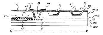
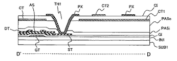
次に、図1及び図6に基づいて、実施形態1の液晶表示装置の第1基板の詳細構成について説明する。なお、以下の説明では1画素分について説明するが、他の画素構造も同じ構成であることはいうまでもない。また、説明を簡単にするために複数の線状電極として2本の画素電極が櫛歯状に形成される場合について説明するが、これに限定されることはなく3本以上の画素電極を櫛歯状に配置した形状にも適用できるものである。 Next, based on FIG.1 and FIG.6, the detailed structure of the 1st board | substrate of the liquid crystal display device of Embodiment 1 is demonstrated. In the following description, one pixel is described, but it goes without saying that other pixel structures have the same configuration. Further, in order to simplify the description, a case where two pixel electrodes are formed in a comb shape as a plurality of linear electrodes will be described, but the present invention is not limited to this, and three or more pixel electrodes are combined. The present invention can also be applied to shapes arranged in a tooth shape.
図6に示すように、実施形態1の液晶表示装置の第1基板では、面状に形成される対向電極CTの上層に形成した容量絶縁膜CIを介して画素電極PXが配置される構成となっている。対向電極CTは透明電極材料であるITO(Indium Tin Oxide)で形成され、コンタクトホールTH2を通してコモン線CLに接続されている。また画素電極PXも櫛歯状に形成されたITOで構成されており、平坦化膜PASoと保護絶縁膜PASiに形成されたコンタクトホールTH1を通して薄膜トランジスタTFTのソース電極STに電気的に接続されている。一方、ドレイン線DLはゲート線GLとの交差部の一部において薄膜トランジスタTFTの形成領域側に延在され、この延在部が半導体層ASの上面にまで及んで薄膜トランジスタTFTのドレイン電極DTを構成している。 As shown in FIG. 6, in the first substrate of the liquid crystal display device according to the first embodiment, the pixel electrode PX is arranged via the capacitive insulating film CI formed on the upper layer of the counter electrode CT formed in a planar shape. It has become. The counter electrode CT is made of ITO (Indium Tin Oxide), which is a transparent electrode material, and is connected to the common line CL through the contact hole TH2. The pixel electrode PX is also made of ITO formed in a comb shape, and is electrically connected to the source electrode ST of the thin film transistor TFT through the contact hole TH1 formed in the planarizing film PASo and the protective insulating film PASi. . On the other hand, the drain line DL extends to the formation region side of the thin film transistor TFT at a part of the intersection with the gate line GL, and this extended portion reaches the upper surface of the semiconductor layer AS to form the drain electrode DT of the thin film transistor TFT. is doing.
画素PIXはゲート線GLからのゲート信号によってオンされる薄膜トランジスタTFTと、このオンされた薄膜トランジスタTFTを介してドレイン線DLからのドレイン信号が供給される画素電極PXと、コモン信号が印加されて画素電極PXとの間の電位差によって電界を生じさせる対向電極CTとを備える。画素電極PXと対向電極CTはともに同じ基板である第1基板SUB1に形成されており、電界は第1基板SUB1の表面と平行な電界成分を一部に含むものである。 The pixel PIX includes a thin film transistor TFT that is turned on by a gate signal from the gate line GL, a pixel electrode PX to which a drain signal from the drain line DL is supplied via the turned on thin film transistor TFT, and a common signal applied to the pixel PIX. And a counter electrode CT that generates an electric field due to a potential difference with the electrode PX. The pixel electrode PX and the counter electrode CT are both formed on the first substrate SUB1, which is the same substrate, and the electric field partially includes an electric field component parallel to the surface of the first substrate SUB1.
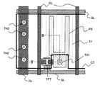
このように、実施形態1の液晶表示装置の第1基板では、トレンチ(溝)TFの底部に形成された対向電極CTの上部に容量絶縁膜CIを介して画素電極PXが重畳して形成されると共に、トレンチ領域外の対向電極CTが画素電極PXと同層に形成され、トレンチ底部とトレンチ領域外の対向電極CTはトレンチ辺縁部も含めて一体に形成されているので、その形成場所によらず同じ電位のコモン信号が入力される構成となっている。 As described above, in the first substrate of the liquid crystal display device according to the first embodiment, the pixel electrode PX is formed so as to overlap the counter electrode CT formed on the bottom of the trench (groove) TF with the capacitive insulating film CI interposed therebetween. In addition, the counter electrode CT outside the trench region is formed in the same layer as the pixel electrode PX, and the counter electrode CT outside the trench region and the trench region is integrally formed including the trench edge. Regardless of the configuration, a common signal having the same potential is input.
ここで、実施形態1の液晶表示装置の第1基板では、画素電極PXの外周形状に沿ってトレンチTFが形成されており、このトレンチTF領域内に画素電極PXが形成される構成となっている。特に実施の形態1の液晶表示装置の第1基板では、このトレンチTF領域内にのみ容量絶縁膜CIが形成される構成となっており、このトレンチTF領域内の容量絶縁膜CIを介して画素電極PXが対向電極CTに重畳される構成となっている。従って、その表示にかかわる領域では、線状に形成された画素電極PXに対して、トレンチTF領域内の対向電極CTが面状電極として構成されると共に、トレンチTF領域外の対向電極CTで画素電極PXを挟む構成となっている。このとき実施形態1の第1基板では、画素電極PXの大きさは従来の画素電極と同じ大きさに形成されるので、画素電極PXに書き込まれた電荷の保持に必要な保持容量を実現するには十分な構成となっている。 Here, in the first substrate of the liquid crystal display device of Embodiment 1, the trench TF is formed along the outer peripheral shape of the pixel electrode PX, and the pixel electrode PX is formed in the trench TF region. Yes. In particular, the first substrate of the liquid crystal display device according to the first embodiment has a configuration in which the capacitor insulating film CI is formed only in the trench TF region, and the pixel is interposed via the capacitor insulating film CI in the trench TF region. The electrode PX is superposed on the counter electrode CT. Therefore, in the region related to the display, the counter electrode CT in the trench TF region is configured as a planar electrode with respect to the pixel electrode PX formed in a linear shape, and the pixel is formed by the counter electrode CT outside the trench TF region. The electrode PX is sandwiched therebetween. At this time, in the first substrate of the first embodiment, the size of the pixel electrode PX is formed to be the same size as the conventional pixel electrode, so that a storage capacitor necessary for holding the charge written in the pixel electrode PX is realized. It has a sufficient structure.
次に、図1に基づいて、本実施形態1の画素電極と対向電極の構造を詳細に説明する。図1に示すように、実施形態1の液晶表示装置の第1基板では、ガラス基板SUB1の上層に薄膜トランジスタTFTを保護するための下地膜IN1が形成され、その上層にゲート電極GT及びゲート絶縁膜GI、半導体層AS、ドレイン電極DT、ソース電極ST等からなる薄膜トランジスタTFTが形成されている。この薄膜トランジスタTFTを図示しない液晶層に含まれるアルカリ成分から保護するために、薄膜トランジスタTFTの上層の全面に保護絶縁膜PASiが形成されている。この保護絶縁膜PASiの上層には平坦化層PASoが積層されている。 Next, the structure of the pixel electrode and the counter electrode according to the first embodiment will be described in detail with reference to FIG. As shown in FIG. 1, in the first substrate of the liquid crystal display device of Embodiment 1, a base film IN1 for protecting the thin film transistor TFT is formed on the upper layer of the glass substrate SUB1, and the gate electrode GT and the gate insulating film are formed on the upper layer. A thin film transistor TFT composed of GI, semiconductor layer AS, drain electrode DT, source electrode ST, and the like is formed. In order to protect the thin film transistor TFT from an alkali component contained in a liquid crystal layer (not shown), a protective insulating film PASi is formed on the entire upper surface of the thin film transistor TFT. A planarizing layer PASo is laminated on the protective insulating film PASi.
ここで、本実施形態1の表示装置の第1基板では、平坦化層PASoの上部にトレンチTFが形成されており、このトレンチTF表面を含む平坦化層PASoの上部表面に対向電極CTが形成されている。従って、画素PIXの表示にかかわる領域では、平坦化膜PASoの上部に形成された線状の対向電極CTの間に、線状の画素電極PXが配置される構成となる。また、トレンチTF領域に形成された対向電極CTの上層には容量絶縁膜CIが平坦化層PASoの高さまで形成されており、このトレンチTF領域の容量絶縁膜CIの上層にのみ画素電極PXが形成される構成となっている。なお、図1に示す断面図のB−B'線方向の中心部分に形成されるトレンチTFは図6から明らかなように、2本の画素電極PXを接続する領域に対応したトレンチTF領域となるので、表示性能に影響するものではない。 Here, in the first substrate of the display device according to the first embodiment, the trench TF is formed on the planarizing layer PASo, and the counter electrode CT is formed on the upper surface of the planarizing layer PASo including the surface of the trench TF. Has been. Accordingly, in the region related to the display of the pixel PIX, the linear pixel electrode PX is arranged between the linear counter electrodes CT formed on the planarizing film PASo. In addition, the capacitive insulating film CI is formed up to the level of the planarization layer PASo in the upper layer of the counter electrode CT formed in the trench TF region, and the pixel electrode PX is formed only in the upper layer of the capacitive insulating film CI in the trench TF region. It is the structure formed. Note that the trench TF formed in the central portion in the BB ′ line direction of the cross-sectional view shown in FIG. 1 is a trench TF region corresponding to a region connecting the two pixel electrodes PX, as is apparent from FIG. Therefore, it does not affect the display performance.
次に、図7に実施形態1の液晶表示装置の対向電極と画素電極を形成ための製造方法の一実施形態を示す工程図を示し、以下、図7に基づいて製造方法を工程順に説明する。なお、各工程における電極の形成を含む薄膜の形成は公知のフォトリソグラフィ技術により可能であるので、詳細な説明は省略する。 Next, FIG. 7 is a process diagram showing an embodiment of a manufacturing method for forming the counter electrode and the pixel electrode of the liquid crystal display device of Embodiment 1, and the manufacturing method will be described below in order of steps based on FIG. . In addition, since formation of the thin film including formation of the electrode in each process is possible by a well-known photolithography technique, detailed description is abbreviate | omitted.
工程1.(図7(a))
ガラス基板SUB1の上面側(液晶側)の面に、下地膜IN1及びゲート電極GT、ゲート絶縁膜GI、半導体層AS、ドレイン電極DT、ソース電極STを形成し、アモルファスシリコンTFTの薄膜トランジスタTFTを形成する。この時、ドレイン線DLおよびドレイン電極DTと同時に形成される薄膜トランジスタTFTのソース電極STが、半導体層AS上にてドレイン電極DTと対向して形成されている。また、ソース電極STは、半導体層AS上から半導体層ASが形成されていない領域に至って延在され、この延在部はパッド部を構成するようになっている。このパッド部は後述の工程で画素電極PXと電気的及び物理的に接続される部分となる。
Step 1. (Fig. 7 (a))
A base film IN1, a gate electrode GT, a gate insulating film GI, a semiconductor layer AS, a drain electrode DT, and a source electrode ST are formed on the upper surface (liquid crystal side) of the glass substrate SUB1, and an amorphous silicon TFT thin film transistor TFT is formed. To do. At this time, the source electrode ST of the thin film transistor TFT formed simultaneously with the drain line DL and the drain electrode DT is formed opposite to the drain electrode DT on the semiconductor layer AS. Further, the source electrode ST extends from the semiconductor layer AS to a region where the semiconductor layer AS is not formed, and this extended portion constitutes a pad portion. This pad portion is a portion that is electrically and physically connected to the pixel electrode PX in a process described later.
工程2.(図7(b))
薄膜トランジスタTFTを保護する無機質材料である窒化シリコン膜からなる保護絶縁膜PASiをガラス基板SUB1の上面側の全面に形成し、薄膜トランジスタTFTの保護膜とする。この保護絶縁膜PASiの上層(基板の液晶側)に公知のスピンコート法等により、アクリル膜からなる平坦化膜PASoをガラス基板の上面側に形成し、薄膜トランジスタTFTをはじめとしたゲート線GL、ドレイン線DL、コモン線CL等の形成に伴うガラス基板上面の凹凸を平坦化する。なお、実施形態1の液晶表示装置の第1基板では保護絶縁膜PASiと平坦化膜PASoとで保護膜を構成している。
Step 2. (Fig. 7 (b))
A protective insulating film PASi made of a silicon nitride film, which is an inorganic material for protecting the thin film transistor TFT, is formed on the entire upper surface of the glass substrate SUB1 to form a protective film for the thin film transistor TFT. A flattening film PASo made of an acrylic film is formed on the upper surface side of the glass substrate by a known spin coating method or the like on the upper layer (the liquid crystal side of the substrate) of the protective insulating film PASi, and the gate lines GL including the thin film transistors TFT, The unevenness on the upper surface of the glass substrate accompanying the formation of the drain line DL, the common line CL, etc. is flattened. In the first substrate of the liquid crystal display device according to the first embodiment, the protective insulating film PASi and the planarizing film PASo constitute a protective film.
次に、平坦化膜PASoの上面(液晶側面)に公知の技術により櫛歯状のトレンチTFを形成する。 Next, a comb-like trench TF is formed on the upper surface (liquid crystal side surface) of the planarizing film PASo by a known technique.
工程3.(図7(c))
従来の対向電極と同じ領域に、透明電極材料であるITOで対向電極CTを形成する。このとき、実施形態1ではエッチングで形成されたトレンチTFの底部からトレンチTFの縁に沿いエッチングされていない領域までの上層部分が対向電極CTで覆われた構造となる。
The counter electrode CT is formed of ITO, which is a transparent electrode material, in the same region as the conventional counter electrode. At this time, the first embodiment has a structure in which the upper layer portion from the bottom of the trench TF formed by etching to the region not etched along the edge of the trench TF is covered with the counter electrode CT.
次に、塗布型絶縁膜を成膜し200度程度の熱処理により焼成処理を行うことにより、ガラス基板の上面に容量絶縁膜CIを形成する。このとき、対向電極CTとなるITO膜も同時に熱処理されるため、ITO膜がアモルファス状態から多結晶状態に変化する。この多結晶ITO膜は、アモルファスITO膜のエッチング条件ではほとんど加工されないため、後に画素電極PXを形成するためのITO加工時において、対向電極CTとなるITO膜が同時に加工されることはない。 Next, a capacitive insulating film CI is formed on the upper surface of the glass substrate by forming a coating type insulating film and performing a baking process by a heat treatment of about 200 degrees. At this time, since the ITO film serving as the counter electrode CT is also heat-treated at the same time, the ITO film changes from an amorphous state to a polycrystalline state. Since this polycrystalline ITO film is hardly processed under the etching conditions of the amorphous ITO film, the ITO film to be the counter electrode CT is not simultaneously processed at the time of ITO processing for forming the pixel electrode PX later.
工程4.(図7(d))
容量絶縁膜CIを平坦化膜PASoの高さまでエッチングすることによって、平坦化膜PASoのトレンチTF部分以外の対向電極CTを容量絶縁膜CIから露出させると共に、トレンチTF部分のみに容量絶縁膜CIを形成する。この工程により、画素電極PXと同層に形成される線状の対向電極CTを形成する。ただし、容量絶縁膜CIの高さは対向電極CTとなるITO膜よりも低くなるように形成することが望ましい。
Step 4. (Fig. 7 (d))
The counter electrode CT other than the trench TF portion of the planarizing film PASo is exposed from the capacitive insulating film CI by etching the capacitive insulating film CI to the level of the planarizing film PASo, and the capacitive insulating film CI is formed only in the trench TF portion. Form. By this step, a linear counter electrode CT formed in the same layer as the pixel electrode PX is formed. However, it is desirable to form the capacitor insulating film CI so that the height thereof is lower than that of the ITO film serving as the counter electrode CT.
工程5(図7(e))
平坦化層PASoと保護絶縁膜PASiにコンタクトホールTH1を形成する。
Step 5 (FIG. 7 (e))
A contact hole TH1 is formed in the planarization layer PASo and the protective insulating film PASi.
工程6(図1)
コンタクトホール部分TH1とトレンチTFが形成される領域内にITO膜を形成することにより、薄膜トランジスタTFTのソース電極STに接続される画素電極PXを形成する。この工程により、線状の対向電極CTの間に、該対向電極CTと同層である線状の画素電極PXが形成される。
Step 6 (FIG. 1)
By forming an ITO film in a region where the contact hole portion TH1 and the trench TF are formed, the pixel electrode PX connected to the source electrode ST of the thin film transistor TFT is formed. By this step, a linear pixel electrode PX that is the same layer as the counter electrode CT is formed between the linear counter electrodes CT.
図18は、実施形態1に基づく本発明の液晶表示装置の断面図である。図18に示すように、実施形態1の液晶表示装置はブラックマトリックスBM及びカラーフィルタCF、配向膜ORI2が形成されるガラス基板(第2の基板)SUB2と実施形態1のガラス基板(第1の基板)SUB1とで液晶LCを挟持する構成となっており、2枚のガラス基板SUB1、SUB2の両側に偏光板PLが形成されている。 FIG. 18 is a cross-sectional view of the liquid crystal display device of the present invention based on the first embodiment. As shown in FIG. 18, the liquid crystal display device of Embodiment 1 includes a glass substrate (second substrate) SUB2 on which a black matrix BM, a color filter CF, and an alignment film ORI2 are formed, and a glass substrate (first substrate) of Embodiment 1. The liquid crystal LC is sandwiched between the substrate SUB1 and the polarizing plate PL is formed on both sides of the two glass substrates SUB1 and SUB2.
従来の液晶表示装置は、図4に示すように、対向電極CTが容量絶縁膜CIに覆われているため、液晶容量Clcに絶縁膜容量Cst2が直列接続される構造となっていた。 As shown in FIG. 4, the conventional liquid crystal display device has a structure in which the insulating film capacitor Cst2 is connected in series to the liquid crystal capacitor Clc because the counter electrode CT is covered with the capacitor insulating film CI.
それに対して、本発明の実施形態1の液晶表示装置では、図18に示すように液晶容量Clcを形成する領域において対向電極CTが容量絶縁膜CIに覆われておらず、対向電極CTと配向膜ORI1が接しているため液晶容量Clcのみが形成される構造となっている。さらには、画素電極PXの下部には容量絶縁膜CIを介して対向電極CTが形成されており、透明な保持容量を形成することにより、高開口率を実現できる。なお、図18は実施形態1を用いた断面構造であるが、実施形態2から5を用いても同様な効果が得られる。 On the other hand, in the liquid crystal display device according to the first embodiment of the present invention, the counter electrode CT is not covered with the capacitor insulating film CI in the region where the liquid crystal capacitor Clc is formed as shown in FIG. Since the film ORI1 is in contact, only the liquid crystal capacitance Clc is formed. Furthermore, the counter electrode CT is formed below the pixel electrode PX via the capacitor insulating film CI, and a high aperture ratio can be realized by forming a transparent storage capacitor. FIG. 18 shows a cross-sectional structure using the first embodiment, but the same effect can be obtained by using the second to fifth embodiments.
以上説明したように、本実施形態1の液晶表示装置では画素PIXの表示にかかわる領域では、平坦化膜PASoの上部に形成された線状の対向電極CTの間に、線状の画素電極PXが配置される構成となるので、平坦化膜PASoの上面(溝と溝の間)に形成された対向電極CTと画素電極PXとの間に容量絶縁膜CIが介在しない構成とすることができる。その結果、液晶駆動信号は容量絶縁膜内部又は液晶/容量絶縁膜界面の固定電荷の影響をほとんど受けない構成とすることができるので、フリッカを大幅に低減させた液晶表示装置を提供することができる。 As described above, in the liquid crystal display device according to the first embodiment, in the region related to the display of the pixel PIX, the linear pixel electrode PX is interposed between the linear counter electrodes CT formed on the planarizing film PASo. Therefore, the capacitor insulating film CI can be configured not to be interposed between the counter electrode CT and the pixel electrode PX formed on the upper surface (between the grooves) of the planarizing film PASo. . As a result, the liquid crystal drive signal can be configured to be hardly affected by the fixed charge inside the capacitive insulating film or at the liquid crystal / capacitor insulating film interface, so that a liquid crystal display device with greatly reduced flicker can be provided. it can.
また、容量絶縁膜CIがトレンチTFを埋め込んだ構造となっているので、ガラス基板SUB1の上面の段差もITO電極の膜厚程度に抑えることが可能となるので、配向膜ORI1のラビング不良を効果的に抑制できる。 In addition, since the capacitor insulating film CI has a structure in which the trench TF is embedded, the step on the upper surface of the glass substrate SUB1 can be suppressed to about the film thickness of the ITO electrode, which effectively prevents the alignment film ORI1 from rubbing. Can be suppressed.
また、容量絶縁膜CIの高さを対向電極CTよりも低くすることにより、画素電極PXと対向電極CTとの間の電界を強くすることができるので、液晶LCの応答を速くすることができる。 Further, since the electric field between the pixel electrode PX and the counter electrode CT can be strengthened by making the height of the capacitor insulating film CI lower than that of the counter electrode CT, the response of the liquid crystal LC can be accelerated. .
(実施形態2)
図8は本発明の実施形態2の液晶表示装置の概略構成を説明するための断面図である。ただし、図8は実施形態1の図1に相当する第1基板の断面図であり、図6のB−B'線での断面図に相当する。なお、実施形態2のLCD構成図、画素平面図は、それぞれ図5、図6と同様である。
(Embodiment 2)
FIG. 8 is a cross-sectional view for explaining a schematic configuration of a liquid crystal display device according to Embodiment 2 of the present invention. 8 is a cross-sectional view of the first substrate corresponding to FIG. 1 of the first embodiment, and corresponds to a cross-sectional view taken along line BB ′ of FIG. The LCD configuration diagram and pixel plan view of the second embodiment are the same as those in FIGS. 5 and 6, respectively.
図8から明らかなように、実施形態2の液晶表示装置では平坦化膜PASoの上面側(図示しない液晶層LC側)に対向電極CTや画素電極PX等が形成される構成となっているので、以下の説明では実施形態1の液晶表示装置と構成が異なるトレンチ絶縁膜TI、対向電極CT、容量絶縁膜CI、画素電極PXの構成について詳細に説明する。 As is apparent from FIG. 8, the liquid crystal display device according to the second embodiment has a configuration in which the counter electrode CT, the pixel electrode PX, and the like are formed on the upper surface side (the liquid crystal layer LC side not shown) of the planarizing film PASo. In the following description, the configuration of the trench insulating film TI, the counter electrode CT, the capacitor insulating film CI, and the pixel electrode PX, which are different in configuration from the liquid crystal display device of Embodiment 1, will be described in detail.
図8において、実施形態2の液晶表示装置では平坦化膜PASoの上層に、例えば窒化シリコン膜等からなるトレンチ絶縁膜TIが形成される構成となっている。このトレンチ絶縁膜TIが形成される領域の内で、画素電極PXが形成される領域には平坦化膜PASoに達するトレンチ(溝)TFが形成されている。一方、コンタクトホールTH1の形成領域を除く画素領域に対向電極CTが形成される構成となっているので、トレンチ絶縁膜TIの上層のみならずトレンチ(溝)TFの底部(露出された平坦化層PASo)からその辺縁部にかけて、所定膜厚の対向電極CTが形成されている。従って、画素PIXの表示にかかわる領域では、トレンチ絶縁膜TIに形成された線状の対向電極CTの間に、線状の画素電極PXが配置される構成となる。 In FIG. 8, the liquid crystal display device according to the second embodiment has a configuration in which a trench insulating film TI made of, for example, a silicon nitride film or the like is formed on the planarizing film PASo. Of the region where the trench insulating film TI is formed, a trench (groove) TF reaching the planarizing film PASo is formed in the region where the pixel electrode PX is formed. On the other hand, since the counter electrode CT is formed in the pixel region excluding the formation region of the contact hole TH1, not only the upper layer of the trench insulating film TI but also the bottom (exposed planarizing layer) of the trench (groove) TF. A counter electrode CT having a predetermined film thickness is formed from PASo) to the edge thereof. Therefore, in the region related to the display of the pixel PIX, the linear pixel electrode PX is arranged between the linear counter electrodes CT formed in the trench insulating film TI.
ここで、実施形態2の液晶表示装置においても、実施形態1の液晶表示装置同様に、トレンチTFが形成された領域(以下、トレンチ領域と記す)内の対向電極CTの上層には容量絶縁膜CIがトレンチ絶縁膜TIと同等の高さまで形成されている。さらには、このトレンチ領域のみに形成された容量絶縁膜CIの上層のみに画素電極PXが形成される構成となっている。ただし、コンタクトホールTH1部分や櫛歯状の画素電極PXを接続する部分はこの限りではない。 Here, also in the liquid crystal display device of the second embodiment, like the liquid crystal display device of the first embodiment, a capacitive insulating film is formed on the counter electrode CT in a region where the trench TF is formed (hereinafter referred to as a trench region). CI is formed to the same height as the trench insulating film TI. Further, the pixel electrode PX is formed only in the upper layer of the capacitor insulating film CI formed only in the trench region. However, the contact hole TH1 portion and the portion to which the comb-like pixel electrode PX is connected are not limited to this.
次に、図9に実施形態2の液晶表示装置の対向電極と画素電極を形成ための製造方法の一実施形態を示す工程図を示し、以下、図9に基づいて製造方法を工程順に説明する。なお、実施形態1と同様に、各工程における電極の形成を含む薄膜の形成は公知のフォトリソグラフィ技術により可能であるので、詳細な説明は省略する。 Next, FIG. 9 is a process diagram showing an embodiment of a manufacturing method for forming the counter electrode and the pixel electrode of the liquid crystal display device of Embodiment 2, and the manufacturing method will be described in the order of steps based on FIG. . As in the first embodiment, since a thin film including an electrode in each step can be formed by a known photolithography technique, a detailed description is omitted.
工程1.(図9(a))
ガラス基板SUB1の液晶側の面に、下地膜IN1及びゲート電極GT、ゲート絶縁膜GI、半導体層AS、ドレイン電極DT、ソース電極STを形成し、アモルファスシリコンTFTの薄膜トランジスタTFTを形成する。なお、この工程1は実施形態1の工程1と同じである。
Step 1. (Fig. 9 (a))
A base film IN1, a gate electrode GT, a gate insulating film GI, a semiconductor layer AS, a drain electrode DT, and a source electrode ST are formed on the liquid crystal side surface of the glass substrate SUB1, and a thin film transistor TFT of an amorphous silicon TFT is formed. This step 1 is the same as step 1 in the first embodiment.
工程2.(図9(b))
薄膜トランジスタTFTを保護するために無機質材料である窒化シリコン膜からなる保護絶縁膜PASiをガラス基板SUB1の上面側(基板の液晶側)の全面に形成し、薄膜トランジスタTFTの保護膜とする。この保護絶縁膜PASiの上層(基板の液晶側)に公知のスピンコート法等により、アクリル膜からなる平坦化膜PASoをガラス基板SUB1の上面側に形成し、薄膜トランジスタTFTをはじめとしたゲート線GL、ドレイン線DL、コモン線CL等の形成に伴うガラス基板SUB1の上面の凹凸を平坦化する。なお、工程2における平坦化膜PASoの形成までの工程は、実施形態1と同じである。また、本実施形態2の液晶表示装置の第1基板SUB1においても保護絶縁膜PASiと平坦化膜PASoとで保護膜を構成する。
Step 2. (Fig. 9 (b))
In order to protect the thin film transistor TFT, a protective insulating film PASi made of a silicon nitride film, which is an inorganic material, is formed on the entire upper surface side (liquid crystal side of the substrate) of the glass substrate SUB1 to form a protective film for the thin film transistor TFT. A planarizing film PASo made of an acrylic film is formed on the upper surface side of the glass substrate SUB1 by a known spin coating method or the like on the protective insulating film PASi (on the liquid crystal side of the substrate), and gate lines GL including the thin film transistors TFT are formed. Then, the unevenness on the upper surface of the glass substrate SUB1 accompanying the formation of the drain line DL, the common line CL, etc. is flattened. The steps up to the formation of the planarizing film PASo in step 2 are the same as those in the first embodiment. Also, in the first substrate SUB1 of the liquid crystal display device according to the second embodiment, the protective insulating film PASi and the planarizing film PASo constitute a protective film.
次に、平坦化膜PASoの上層に例えば窒化シリコン膜からなるトレンチ絶縁膜TIを成膜する。その後、このトレンチ絶縁膜TIを平坦化膜PASoが露出するまでエッチングし、トレンチTFを形成する。なお、トレンチ絶縁膜TIのエッチング領域は実施形態1と同様に、後の工程で画素電極PXが形成される領域である。また、トレンチ絶縁膜TIのエッチング量を制御することによりトレンチTIの深さを制御することは可能であるが、トレンチ絶縁膜TIの膜厚を制御し平坦化膜PASoまでエッチングしてトレンチTIを形成する方が、より正確にトレンチTIの深さを制御可能である。 Next, a trench insulating film TI made of, for example, a silicon nitride film is formed on the planarizing film PASo. Thereafter, the trench insulating film TI is etched until the planarizing film PASo is exposed, thereby forming a trench TF. It should be noted that the etching region of the trench insulating film TI is a region where the pixel electrode PX is formed in a later process, as in the first embodiment. Although the depth of the trench TI can be controlled by controlling the etching amount of the trench insulating film TI, the trench TI is etched by controlling the film thickness of the trench insulating film TI and etching to the planarizing film PASo. When formed, the depth of the trench TI can be controlled more accurately.
工程3.(図9(c))
実施形態1と同様に、透明電極材料であるITOで対向電極CTを形成する。このとき、エッチングで形成されたトレンチTIの底部からトレンチTIの縁に沿いエッチングされていない領域までの上層部分がITO膜で形成された対向電極CTで覆われた構造となる。
Similar to the first embodiment, the counter electrode CT is formed of ITO, which is a transparent electrode material. At this time, the upper layer portion from the bottom of the trench TI formed by etching to the region not etched along the edge of the trench TI is covered with the counter electrode CT formed of an ITO film.
次に、塗布型絶縁膜を成膜し200度程度の熱処理により焼成処理を行うことにより、ガラス基板SUB1の上面側の全面に容量絶縁膜CIを形成する。なお、このときも実施形態1における容量絶縁膜CIの形成時と同様に、対向電極CTとなるITO膜も同時に熱処理されるため、ITO膜がアモルファス状態から多結晶状態に変化する。 Next, a capacitive insulating film CI is formed on the entire upper surface of the glass substrate SUB1 by forming a coating type insulating film and performing a baking process by a heat treatment of about 200 degrees. At this time, as in the formation of the capacitive insulating film CI in the first embodiment, the ITO film to be the counter electrode CT is also heat-treated at the same time, so that the ITO film changes from an amorphous state to a polycrystalline state.
工程4.(図9(d))
容量絶縁膜CIをトレンチ絶縁膜TIの高さまでエッチングすることによって、トレンチTF部分以外の対向電極CTを容量絶縁膜CIから露出させると共に、トレンチTF部分のみに容量絶縁膜CIを形成する。この工程により、画素電極PXと同層に形成される線状の対向電極CTを形成する。ただし、要領絶縁膜CIの高さは対向電極CTとなるITO膜よりも低くなるように形成することが望ましい。
Step 4. (Fig. 9 (d))
By etching the capacitive insulating film CI to the height of the trench insulating film TI, the counter electrode CT other than the trench TF portion is exposed from the capacitive insulating film CI, and the capacitive insulating film CI is formed only in the trench TF portion. By this step, a linear counter electrode CT formed in the same layer as the pixel electrode PX is formed. However, it is desirable to form the insulating film CI so that its height is lower than that of the ITO film serving as the counter electrode CT.
工程5(図9(e))
トレンチ絶縁膜TIから平坦化層PASoと保護絶縁膜PASiを貫通し、ソース電極STのパッド部に達するコンタクトホールTH1を形成する。
Step 5 (FIG. 9 (e))
A contact hole TH1 that penetrates the planarization layer PASo and the protective insulating film PASi from the trench insulating film TI and reaches the pad portion of the source electrode ST is formed.
工程6(図8)
コンタクトホールTH1部分とトレンチTFが形成される領域内にITOを電極材料とする画素電極PXを形成することにより、薄膜トランジスタTFTのソース電極STに接続される画素電極PXを形成する。この工程により、線状の対向電極CTの間に、この対向電極CTと同層となる線状の画素電極PXが形成される。
Step 6 (FIG. 8)
A pixel electrode PX connected to the source electrode ST of the thin film transistor TFT is formed by forming the pixel electrode PX using ITO as an electrode material in a region where the contact hole TH1 portion and the trench TF are formed. By this step, a linear pixel electrode PX that is the same layer as the counter electrode CT is formed between the linear counter electrodes CT.
以上説明したように、実施形態2の液晶表示装置においても、画素PIXの表示にかかわる領域では、トレンチ絶縁膜TIの上面に形成された線状の対向電極CTの間に線状の画素電極PXが配置される構成となるので、トレンチ絶縁膜TIの上面(溝と溝の間)に形成された対向電極CTと画素電極PXとの間に容量絶縁膜CIが介在しない構成となる。従って、液晶駆動信号は容量絶縁膜内部又は液晶/容量絶縁膜界面の固定電荷の影響をほとんど受けない構成とすることができるので、フリッカを大幅に低減させた液晶表示装置を提供することができる。 As described above, also in the liquid crystal display device of the second embodiment, in the region related to the display of the pixel PIX, the linear pixel electrode PX is disposed between the linear counter electrodes CT formed on the upper surface of the trench insulating film TI. Therefore, the capacitor insulating film CI is not interposed between the counter electrode CT and the pixel electrode PX formed on the upper surface (between the grooves) of the trench insulating film TI. Therefore, the liquid crystal drive signal can be configured to be hardly affected by the fixed charge inside the capacitive insulating film or at the liquid crystal / capacitor insulating film interface, so that it is possible to provide a liquid crystal display device with greatly reduced flicker. .
また、容量絶縁膜CIがトレンチTFを埋め込んだ構造となっているので、ガラス基板SUB1の上面の段差もITO電極の膜厚程度に抑えることが可能となるので、配向膜のラビング不良を効果的に抑制できる。 In addition, since the capacitor insulating film CI has a structure in which the trench TF is embedded, the step on the upper surface of the glass substrate SUB1 can be suppressed to the thickness of the ITO electrode, which effectively prevents the alignment film from rubbing. Can be suppressed.
また、容量絶縁膜CIの高さを対向電極CTよりも低くすることにより、画素電極PXと対向電極CTとの間の電界が強くすることができるので、液晶の応答を速くすることができる。 In addition, since the electric field between the pixel electrode PX and the counter electrode CT can be increased by making the height of the capacitor insulating film CI lower than that of the counter electrode CT, the response of the liquid crystal can be accelerated.
前述する効果に加えて、実施形態2の液晶表示装置では、トレンチTFを形成するための膜(トレンチ絶縁膜TI)を平坦化膜PASoとは別に設け、その膜をエッチング加工することによりトレンチTFを形成するので、トレンチ深さ等の制御が容易である。従って、トレンチTIを浅く形成する(すなわち、容量絶縁膜CIを薄く形成する)ことが容易に可能となり、(第1基板SUB1の上面側(図示しない液晶層LC側)の平坦性を損なうことなく)保持容量を大きくできるという格別の効果を得ることが可能となる。 In addition to the effects described above, in the liquid crystal display device according to the second embodiment, a film (trench insulating film TI) for forming the trench TF is provided separately from the planarizing film PASo, and the film is etched to form the trench TF. Therefore, the trench depth and the like can be easily controlled. Therefore, it is possible to easily form the trench TI shallowly (that is, to form the capacitor insulating film CI thin) without impairing the flatness on the upper surface side (the liquid crystal layer LC side not shown) of the first substrate SUB1. ) It is possible to obtain a special effect that the storage capacity can be increased.
(実施形態3)
図10は本発明の実施形態1の液晶表示装置の概略構成を説明するための1画素分の液晶表示素子の平面図であり、図11は図10に示すC−C'線での断面図である。
(Embodiment 3)
FIG. 10 is a plan view of a liquid crystal display element for one pixel for explaining a schematic configuration of the liquid crystal display device according to the first embodiment of the present invention, and FIG. 11 is a cross-sectional view taken along line CC ′ shown in FIG. It is.
図10から明らかなように、実施形態3の液晶表示装置では平坦化膜PASoにトレンチTFを形成し、このトレンチTF領域に容量絶縁膜CIを介して画素電極PXを形成する構成となっているので、以下の説明では実施の形態1の液晶表示装置と構成が異なるコンタクトホールTH1の構成について詳細に説明する。 As is apparent from FIG. 10, the liquid crystal display device according to the third embodiment has a configuration in which a trench TF is formed in the planarizing film PASo, and a pixel electrode PX is formed in the trench TF region via a capacitive insulating film CI. Therefore, in the following description, the configuration of the contact hole TH1 having a configuration different from that of the liquid crystal display device of the first embodiment will be described in detail.
図10に示す実施形態3の液晶表示装置は、薄膜トランジスタTFTのソース電極STと画素電極PXとを電気的に接続するためのコンタクトホールTH1が形成される領域に、対向電極CTを形成するのと同じITOを用いてコンタクトホール電極THTが形成される構成となっている。コンタクトホール電極THTの一方はソース電極STに電気的に接続される構成となっており、他方は画素電極PXに電気的に接続される構成となっている。このとき、図10から明らかなように、対向電極CTとコンタクトホール電極THTとが電気的に接続されないように、対向電極CTとコンタクトホール電極THTとは所定の距離を保って形成されている。
In the liquid crystal display device of
また、図11に示すように、実施の形態3の液晶表示装置ではコンタクトホール電極THTの上層に容量絶縁膜CIが平坦化膜PASoの高さまで形成されており、この容量絶縁膜CIとコンタクトホール電極THTの上層に画素電極PXが形成される構成となっている。一方、薄膜トランジスタTFTや画素電極PXが形成される領域の上面(液晶層)側は、実施の形態1の液晶表示装置と同じ構成となっているので、ガラス基板SUB1の上面全体の段差もITO電極の膜厚程度に抑えることが可能となっている。その結果、図示しない配向膜のラビング不良を効果的に抑制できる。 As shown in FIG. 11, in the liquid crystal display device according to the third embodiment, the capacitive insulating film CI is formed up to the level of the planarizing film PASo on the contact hole electrode THT, and the capacitive insulating film CI and the contact hole are formed. The pixel electrode PX is formed on the upper layer of the electrode THT. On the other hand, the upper surface (liquid crystal layer) side of the region where the thin film transistor TFT and the pixel electrode PX are formed has the same configuration as that of the liquid crystal display device of the first embodiment, so The film thickness can be suppressed to about the same. As a result, it is possible to effectively suppress the rubbing failure of the alignment film (not shown).
次に、図12に実施形態3の液晶表示装置の製造方法の一実施形態を示す工程図を示し、以下、図12に基づいて製造方法を工程順に説明する。なお、実施形態1、2と同様に、各工程における電極の形成を含む薄膜の形成は公知のフォトリソグラフィ技術により可能であるので、詳細な説明は省略する。
Next, FIG. 12 is a process diagram showing an embodiment of a manufacturing method of the liquid crystal display device of
工程1.(図12(a))
ガラス基板SUB1の液晶LC側の面に、下地膜IN1及びゲート電極GT、ゲート絶縁膜GI、半導体層AS、ドレイン電極DT、ソース電極STを形成し、アモルファスシリコンTFTの薄膜トランジスタTFTを形成する。なお、この工程1は実施形態1、2の工程1と同じである。
Step 1. (Fig. 12 (a))
A base film IN1, a gate electrode GT, a gate insulating film GI, a semiconductor layer AS, a drain electrode DT, and a source electrode ST are formed on the surface of the glass substrate SUB1 on the liquid crystal LC side, and a thin film transistor TFT of an amorphous silicon TFT is formed. In addition, this process 1 is the same as the process 1 of Embodiment 1,2.
工程2.(図12(b))
薄膜トランジスタTFTを保護するために無機質材料である窒化シリコン膜からなる保護絶縁膜PASiをガラス基板SUB1の上面側(基板の液晶LC側)の全面に形成し、薄膜トランジスタTFTの保護膜とする。この保護絶縁膜PASiの上層(基板の液晶LC側)に公知のスピンコート法等により、アクリル膜からなる平坦化膜PASoをガラス基板SUB1の上面側に形成し、薄膜トランジスタTFTをはじめとしたゲート線GL、ドレイン線DL、コモン線CL等の形成に伴うガラス基板SUB1の上面の凹凸を平坦化する。なお、工程2における平坦化膜PASoの形成までの工程は、実施形態1、2と同じである。また、本実施形態3の液晶表示装置の第1基板SUB1においても保護絶縁膜PASiと平坦化膜PASoとで保護膜を構成する。
Step 2. (Fig. 12 (b))
In order to protect the thin film transistor TFT, a protective insulating film PASi made of a silicon nitride film, which is an inorganic material, is formed on the entire upper surface side (the liquid crystal LC side of the substrate) of the glass substrate SUB1 to form a protective film for the thin film transistor TFT. A flattening film PASo made of an acrylic film is formed on the upper surface side of the glass substrate SUB1 by a known spin coating method or the like on the upper layer of the protective insulating film PASi (the liquid crystal LC side of the substrate), and gate lines including thin film transistors TFT are formed. The unevenness on the upper surface of the glass substrate SUB1 accompanying the formation of the GL, the drain line DL, the common line CL, etc. is flattened. The steps up to the formation of the planarizing film PASo in step 2 are the same as those in the first and second embodiments. Also, in the first substrate SUB1 of the liquid crystal display device according to the third embodiment, the protective insulating film PASi and the planarizing film PASo constitute a protective film.
その後、平坦化層PASoと保護絶縁膜PASiを貫通し、ソース電極STのパッド部に達するコンタクトホールTH1を形成する。 Thereafter, a contact hole TH1 that penetrates the planarization layer PASo and the protective insulating film PASi and reaches the pad portion of the source electrode ST is formed.
工程3.(図12(c))
次に、平坦化膜PASoの上面に、画素電極PXの形状に沿ったトレンチTFを形成する。
Next, a trench TF along the shape of the pixel electrode PX is formed on the upper surface of the planarizing film PASo.
工程4.(図12(d))
次に、透明電極材料であるITOで対向電極CTを形成すると共に、コンタクトホールTH1部分にコンタクトホール電極THTを形成する。なお、コンタクトホール電極THTを除く対向電極CTの構成は、実施形態1と同様に構成である。
Step 4. (Fig. 12 (d))
Next, the counter electrode CT is formed of ITO, which is a transparent electrode material, and the contact hole electrode THT is formed in the contact hole TH1. The configuration of the counter electrode CT excluding the contact hole electrode THT is the same as that of the first embodiment.
工程5.(図12(e))
次に、実施形態1と同様に、塗布型絶縁膜を成膜し200度程度の熱処理により焼成処理を行い全面に容量絶縁膜CIを形成し、この容量絶縁膜CIを平坦化膜PASoの高さまでエッチングすることによって、コンタクトホール電極THTの上部とトレンチTF部分以外の対向電極CTを容量絶縁膜CIから露出させる。ただし、容量絶縁膜CIの高さは対向電極CTとなるITO膜よりも低くなるように形成することが望ましい
工程6(図11)
コンタクトホールTH1部分とトレンチTFが形成される領域内にITOを電極材料とする画素電極PXを形成することにより、コンタクトホール電極THTを介して薄膜トランジスタTFTのソース電極STに接続される画素電極PXを形成する。このとき、実施形態3ではコンタクトホールTH1を平坦化しているので、コンタクトホールTH1の上部においても液晶ギャップを均一にできる。
Step 5. (Fig. 12 (e))
Next, as in the first embodiment, a coating-type insulating film is formed and baked by a heat treatment of about 200 ° C. to form a capacitive insulating film CI on the entire surface. This capacitive insulating film CI is formed on the planarizing film PASo. Etching is performed to expose the counter electrode CT other than the upper part of the contact hole electrode THT and the trench TF from the capacitor insulating film CI. However, it is desirable to form the capacitor insulating film CI so that the height thereof is lower than that of the ITO film serving as the counter electrode CT. Step 6 (FIG. 11)
By forming the pixel electrode PX using ITO as an electrode material in the region where the contact hole TH1 portion and the trench TF are formed, the pixel electrode PX connected to the source electrode ST of the thin film transistor TFT via the contact hole electrode THT is formed. Form. At this time, since the contact hole TH1 is flattened in the third embodiment, the liquid crystal gap can be made uniform even above the contact hole TH1.
以上説明したように、実施形態3の液晶表示装置においても、画素電極PXと対向電極CTの構成は実施形態1と同様の構成、すなわち画素PIXの表示にかかわる領域では平坦化膜PASoの上部に形成された線状の対向電極CTの間に線状の画素電極PXが配置される構成となるので、液晶駆動信号は容量絶縁膜内部又は液晶/容量絶縁膜界面の固定電荷の影響をほとんど受けない構成とすることができ、フリッカを大幅に低減させた液晶表示装置を提供することができる。 As described above, also in the liquid crystal display device of the third embodiment, the configuration of the pixel electrode PX and the counter electrode CT is the same as that of the first embodiment, that is, in the region related to the display of the pixel PIX, the upper portion of the planarization film PASo. Since the linear pixel electrode PX is arranged between the formed linear counter electrodes CT, the liquid crystal drive signal is almost affected by the fixed charge inside the capacitor insulating film or at the interface between the liquid crystal / capacitor insulating film. Thus, a liquid crystal display device can be provided in which flicker is greatly reduced.
また、容量絶縁膜CIがトレンチTFを埋め込んだ構造となっているので、ガラス基板SUB1の上面の段差もITO電極の膜厚程度に抑えることが可能となるので、配向膜のラビング不良を効果的に抑制できる。 In addition, since the capacitor insulating film CI has a structure in which the trench TF is embedded, the step on the upper surface of the glass substrate SUB1 can be suppressed to the thickness of the ITO electrode, which effectively prevents the alignment film from rubbing. Can be suppressed.
また、容量絶縁膜CIの高さを対向電極CTよりも低くすることにより、画素電極PXと対向電極CTとの間の電界が強くすることができるので、液晶の応答を速くすることができる。 In addition, since the electric field between the pixel electrode PX and the counter electrode CT can be increased by making the height of the capacitor insulating film CI lower than that of the counter electrode CT, the response of the liquid crystal can be accelerated.
前述する効果に加えて、実施形態3の液晶表示装置では、コンタクトホールTH1を平坦化しているので、コンタクトホールTH1の上部においても液晶ギャップを均一にできるという格別の効果を得ることができる。その結果、コンタクトホールTH1領域における光の屈折等を大幅に低減でき、ブラックマトリクス幅の大幅な低減やブラックマトリクスの廃止等が可能となるので、開口率を向上させることができるという格別の効果を得ることが可能となる。
In addition to the effects described above, in the liquid crystal display device of
(実施形態4)
図13は本発明の実施形態4の液晶表示装置の概略構成を説明するための断面図である。ただし、図13は実施形態1の図1に相当する第1基板の断面図であり、実施形態3の図10のC−C'線での断面図に相当する。なお、実施形態4のLCD構成図、画素平面図は、それぞれ実施形態1の図5、実施形態3の図10と同様である。
(Embodiment 4)
FIG. 13 is a cross-sectional view for explaining a schematic configuration of a liquid crystal display device according to Embodiment 4 of the present invention. 13 is a cross-sectional view of the first substrate corresponding to FIG. 1 of the first embodiment, and corresponds to a cross-sectional view taken along the line CC ′ of FIG. 10 of the third embodiment. The LCD configuration diagram and the pixel plan view of the fourth embodiment are the same as FIG. 5 of the first embodiment and FIG. 10 of the third embodiment, respectively.
図13から明らかなように、実施形態4の液晶表示装置は実施形態2の液晶表示装置の構成に実施形態3の液晶表示装置のコンタクトホールの構成を適応した構成となっている。 As is apparent from FIG. 13, the liquid crystal display device of the fourth embodiment has a configuration in which the configuration of the contact hole of the liquid crystal display device of the third embodiment is adapted to the configuration of the liquid crystal display device of the second embodiment.
すなわち、実施形態4の液晶表示装置は平坦化膜PASoの上層にトレンチ絶縁膜TIが形成され、このトレンチ絶縁膜TIにトレンチTFを形成し、容量絶縁膜CIを介して画素電極PXを形成する構成となっている。また、コンタクトホール部分の構成は、コンタクトホール電極THTの上層に容量絶縁膜CIがトレンチ絶縁膜TIの高さまで形成され、この容量絶縁膜CIとコンタクトホール電極THTの上層に画素電極PXが形成される構成となっている。このとき、対向電極CTとコンタクトホール電極THTとが電気的に接続されないように、対向電極CTとコンタクトホール電極THTとは所定の距離を保って形成されている。 That is, in the liquid crystal display device according to the fourth embodiment, the trench insulating film TI is formed in the upper layer of the planarizing film PASo, the trench TF is formed in the trench insulating film TI, and the pixel electrode PX is formed through the capacitive insulating film CI. It has a configuration. Further, the contact hole portion is configured such that the capacitor insulating film CI is formed up to the height of the trench insulating film TI above the contact hole electrode THT, and the pixel electrode PX is formed above the capacitor insulating film CI and the contact hole electrode THT. It is the composition which becomes. At this time, the counter electrode CT and the contact hole electrode THT are formed at a predetermined distance so that the counter electrode CT and the contact hole electrode THT are not electrically connected.
次に、図14に実施形態4の液晶表示装置の製造方法の一実施形態を示す工程図を示し、以下、図14に基づいて製造方法を工程順に説明する。なお、実施形態1と同様に、各工程における電極の形成を含む薄膜の形成は公知のフォトリソグラフィ技術により可能であるので、詳細な説明は省略する。 Next, FIG. 14 is a process diagram showing an embodiment of a manufacturing method of the liquid crystal display device of Embodiment 4, and the manufacturing method will be described below in the order of steps based on FIG. As in the first embodiment, since a thin film including an electrode in each step can be formed by a known photolithography technique, a detailed description is omitted.
工程1.(図14(a))
ガラス基板SUB1の液晶LC側の面に、下地膜IN1及びゲート電極GT、ゲート絶縁膜GI、半導体層AS、ドレイン電極DT、ソース電極STを形成し、アモルファスシリコンTFTの薄膜トランジスタTFTを形成する。なお、この工程1は実施形態1の工程1と同じである。
Step 1. (Fig. 14 (a))
A base film IN1, a gate electrode GT, a gate insulating film GI, a semiconductor layer AS, a drain electrode DT, and a source electrode ST are formed on the surface of the glass substrate SUB1 on the liquid crystal LC side, and a thin film transistor TFT of an amorphous silicon TFT is formed. This step 1 is the same as step 1 in the first embodiment.
工程2.(図14(b))
薄膜トランジスタTFTを保護するために無機質材料である窒化シリコン膜からなる保護絶縁膜PASiをガラス基板SUB1の上面側(基板の液晶LC側)の全面に形成し、薄膜トランジスタTFTの保護膜とする。この保護絶縁膜PASiの上層(基板の液晶LC側)に公知のスピンコート法等により、アクリル膜からなる平坦化膜PASoをガラス基板SUB1の上面側に形成し、薄膜トランジスタTFTをはじめとしたゲート線GL、ドレイン線DL、コモン線CL等の形成に伴うガラス基板SUB1の上面の凹凸を平坦化する。次に、平坦化膜PASoの上層に例えば窒化シリコン膜からなるトレンチ絶縁膜TIを成膜する。なお、工程2におけるトレンチ絶縁膜TIの形成までの工程は、実施形態2と同じである。また、本実施形態4の液晶表示装置の第1基板SUB1においても保護絶縁膜PASiと平坦化膜PASoとで保護膜を構成する。
Step 2. (Fig. 14 (b))
In order to protect the thin film transistor TFT, a protective insulating film PASi made of a silicon nitride film, which is an inorganic material, is formed on the entire upper surface side (the liquid crystal LC side of the substrate) of the glass substrate SUB1 to form a protective film for the thin film transistor TFT. A flattening film PASo made of an acrylic film is formed on the upper surface side of the glass substrate SUB1 by a known spin coating method or the like on the upper layer of the protective insulating film PASi (the liquid crystal LC side of the substrate), and gate lines including thin film transistors TFT are formed. The unevenness on the upper surface of the glass substrate SUB1 accompanying the formation of the GL, the drain line DL, the common line CL, etc. is flattened. Next, a trench insulating film TI made of, for example, a silicon nitride film is formed on the planarizing film PASo. The steps up to the formation of the trench insulating film TI in step 2 are the same as those in the second embodiment. Also, in the first substrate SUB1 of the liquid crystal display device according to the fourth embodiment, the protective insulating film PASi and the planarizing film PASo constitute a protective film.
この後、このトレンチ絶縁膜TIを平坦化膜PASoが露出するまでエッチングし、対向電極CT及び画素電極PXを形成するトレンチTFとコンタクトホールを形成する部分のトレンチTF1を形成する。 Thereafter, the trench insulating film TI is etched until the planarizing film PASo is exposed, and a trench TF for forming the counter electrode CT and the pixel electrode PX and a trench TF1 for forming a contact hole are formed.
工程3(図14(c))
工程2で形成したトレンチTF1領域内に、平坦化層PASoと保護絶縁膜PASiを貫通し、ソース電極STのパッド部に達するコンタクトホールTH1を形成する。
Step 3 (FIG. 14 (c))
A contact hole TH1 that penetrates the planarization layer PASo and the protective insulating film PASi and reaches the pad portion of the source electrode ST is formed in the region of the trench TF1 formed in step 2.
工程4.(図14(d))
透明電極材料であるITOで対向電極CTを形成すると共に、コンタクトホールTH1部分にコンタクトホール電極THTを形成する。次に、実施形態2と同様に、塗布型絶縁膜を成膜し200度程度の熱処理により焼成処理を行い全面に容量絶縁膜CIを形成し、この容量絶縁膜CIをトレンチ絶縁膜TIの高さまでエッチングすることによって、コンタクトホール電極THTの上部とトレンチTF部分以外の対向電極CTを容量絶縁膜CIから露出させる。
Step 4. (Fig. 14 (d))
The counter electrode CT is formed of ITO, which is a transparent electrode material, and the contact hole electrode THT is formed in the contact hole TH1 portion. Next, as in the second embodiment, a coating type insulating film is formed and baked by a heat treatment of about 200 ° C. to form a capacitive insulating film CI on the entire surface, and this capacitive insulating film CI is formed on the trench insulating film TI. Etching is performed to expose the counter electrode CT other than the upper part of the contact hole electrode THT and the trench TF from the capacitor insulating film CI.
工程5(図13)
コンタクトホールTH1部分とトレンチTFが形成される領域内にITOを電極材料とする画素電極PXを形成することにより、コンタクトホール電極THTを介して薄膜トランジスタTFTのソース電極STに接続される画素電極PXを形成する。このとき、実施形態4でもコンタクトホールTH1を平坦化しているので、コンタクトホールTH1の上部においても液晶ギャップを均一にできる。
Step 5 (FIG. 13)
By forming the pixel electrode PX using ITO as an electrode material in the region where the contact hole TH1 portion and the trench TF are formed, the pixel electrode PX connected to the source electrode ST of the thin film transistor TFT via the contact hole electrode THT is formed. Form. At this time, since the contact hole TH1 is also flattened in the fourth embodiment, the liquid crystal gap can be made uniform even above the contact hole TH1.
以上説明したように、実施形態4の液晶表示装置は実施形態2と実施形態3の液晶表示装置の効果をそれぞれ併せ持つことが出来る。例えば、画素PIXの表示にかかわる領域ではトレンチ絶縁膜TIの上面に形成された線状の対向電極CTの間に線状の画素電極PXが配置される構成となるので、トレンチ絶縁膜TIの上面(溝と溝の間)に形成された対向電極CTと画素電極PXとの間に容量絶縁膜CIが介在しない構成となる。従って、液晶駆動信号は容量絶縁膜内部又は液晶/容量絶縁膜界面の固定電荷の影響をほとんど受けない構成とすることができるので、フリッカを大幅に低減させた液晶表示装置を提供することができる。 As described above, the liquid crystal display device of the fourth embodiment can have the effects of the liquid crystal display devices of the second and third embodiments. For example, in the region related to the display of the pixel PIX, since the linear pixel electrode PX is arranged between the linear counter electrodes CT formed on the upper surface of the trench insulating film TI, the upper surface of the trench insulating film TI is formed. The capacitor insulating film CI is not interposed between the counter electrode CT and the pixel electrode PX (between the grooves). Therefore, the liquid crystal drive signal can be configured to be hardly affected by the fixed charge inside the capacitive insulating film or at the liquid crystal / capacitor insulating film interface, so that it is possible to provide a liquid crystal display device with greatly reduced flicker. .
さらには、実施形態2と実施形態3の液晶表示装置の効果の他に、コンタクトホールの平坦化による開口率の向上および、容量絶縁膜の薄膜化による保持容量の向上を同時に図ることができるという格別の効果を得ることができる。 Furthermore, in addition to the effects of the liquid crystal display devices of the second and third embodiments, it is possible to simultaneously improve the aperture ratio by flattening the contact hole and the retention capacity by thinning the capacitor insulating film. A special effect can be obtained.
(実施形態5)
図15は本発明の実施形態1の液晶表示装置の概略構成を説明するための1画素分の液晶表示素子の平面図であり、図16は図15に示すD−D'線での断面図である。なお、後述するように、画素電極PXと同層に形成された上層対向電極CT2との間には容量絶縁膜CIが介在しないので液晶容量Clcのみが形成され、薄膜トランジスタTFTのソースには保持容量Cst1と液晶容量Clcとが並列に接続されるのみの構成となる。
(Embodiment 5)
FIG. 15 is a plan view of a liquid crystal display element for one pixel for explaining a schematic configuration of the liquid crystal display device according to the first embodiment of the present invention, and FIG. 16 is a cross-sectional view taken along line DD ′ shown in FIG. It is. As will be described later, since the capacitor insulating film CI is not interposed between the pixel electrode PX and the upper counter electrode CT2 formed in the same layer, only the liquid crystal capacitor Clc is formed and the source of the thin film transistor TFT is the storage capacitor. The configuration is such that Cst1 and the liquid crystal capacitor Clc are only connected in parallel.
図15に基づいて、実施形態5の液晶表示装置の第1基板の詳細構成について説明する。なお、以下の説明では1画素分について説明するが、他の画素の構造も同じ構成であることはいうまでもない。また、説明を簡単にするために2本の画素電極PXが櫛歯状に形成される場合について説明するが、これに限定されることはなく3本以上の画素電極PXを櫛歯状に配置した形状にも適用できるものである。 Based on FIG. 15, the detailed structure of the 1st board | substrate of the liquid crystal display device of Embodiment 5 is demonstrated. In the following description, one pixel is described, but it is needless to say that other pixels have the same structure. Further, in order to simplify the description, a case where two pixel electrodes PX are formed in a comb-teeth shape will be described. However, the present invention is not limited to this, and three or more pixel electrodes PX are arranged in a comb-teeth shape. The present invention can also be applied to shapes that have been made.
図15に示すように、実施形態5の液晶表示装置の第1基板SUB1では、下層対向電極CT1と画素電極PXとの位置関係は従来の液晶表示装置と同様の構成であり、下層対向電極CT1の上層に形成した容量絶縁膜CIを介して画素電極PXが配置される構成となっている。 As shown in FIG. 15, in the first substrate SUB1 of the liquid crystal display device of Embodiment 5, the positional relationship between the lower layer counter electrode CT1 and the pixel electrode PX is the same as that of the conventional liquid crystal display device, and the lower layer counter electrode CT1. The pixel electrode PX is arranged through the capacitive insulating film CI formed in the upper layer.
また、実施形態5の液晶表示装置では、画素電極PXと同層すなわち容量絶縁膜CIの上層に上層対向電極CT2が当該容量絶縁膜CIの上面を覆うように形成されている。このとき、画素電極PXと上層対向電極CT2とが電気的に接続しないようにするために、上層対向電極CT2は画素電極PXを避けるように当該画素電極PXの外周に沿って形成されている。従って、画素電極PXが形成される領域では、上層対向電極CT2の形状も櫛歯状に形成されることとなる。 In the liquid crystal display device according to the fifth embodiment, the upper-layer counter electrode CT2 is formed in the same layer as the pixel electrode PX, that is, the upper layer of the capacitor insulating film CI so as to cover the upper surface of the capacitor insulating film CI. At this time, in order to prevent the pixel electrode PX and the upper layer counter electrode CT2 from being electrically connected, the upper layer counter electrode CT2 is formed along the outer periphery of the pixel electrode PX so as to avoid the pixel electrode PX. Therefore, in the region where the pixel electrode PX is formed, the shape of the upper counter electrode CT2 is also formed in a comb shape.
また、上層対向電極CT2はITOで形成され、コンタクトホールTH4を介してコモン線CLに直接接続される。一方、ITOで形成される下層対向電極CT1は、コンタクトホールTH3を介して上層対向電極CT2に接続される構成となっている。従って、下層対向電極CT1と上層対向電極CT2とにコモン信号が供給され、同電位である。 The upper counter electrode CT2 is made of ITO and is directly connected to the common line CL via the contact hole TH4. On the other hand, the lower layer counter electrode CT1 formed of ITO is connected to the upper layer counter electrode CT2 via the contact hole TH3. Therefore, a common signal is supplied to the lower counter electrode CT1 and the upper counter electrode CT2, and has the same potential.
また、画素電極PXも櫛歯状に形成されたITOで構成されており、平坦化膜PASoと保護絶縁膜PASiに形成されたコンタクトホールTH1を通して薄膜トランジスタTFTのソース電極STに電気的に接続されている。従って、画素PIXの表示にかかわる領域では、画素電極PXと同層に形成される線状の上層対向電極CT2の間に画素電極PXが配置される構成となる。 Further, the pixel electrode PX is also made of ITO formed in a comb shape, and is electrically connected to the source electrode ST of the thin film transistor TFT through the contact hole TH1 formed in the planarization film PASo and the protective insulating film PASi. Yes. Accordingly, in the area related to the display of the pixel PIX, the pixel electrode PX is arranged between the linear upper layer counter electrode CT2 formed in the same layer as the pixel electrode PX.
一方、ドレイン線DLはゲート線GLとの交差部の一部において薄膜トランジスタTFTの形成領域側に延在され、この延在部が半導体層ASの上面にまで及んで薄膜トランジスタTFTのドレイン電極DTを構成している。 On the other hand, the drain line DL extends to the formation region side of the thin film transistor TFT at a part of the intersection with the gate line GL, and this extended portion reaches the upper surface of the semiconductor layer AS to form the drain electrode DT of the thin film transistor TFT. is doing.
次に、図16に基づいて、本実施形態1の液晶表示装置の構造を詳細に説明する。図16に示すように、実施形態5の液晶表示装置における第1基板SUB1では、ガラス基板SUB1の上層に薄膜トランジスタTFTを保護するための下地膜IN1が形成され、その上層にゲート電極GT及びゲート絶縁膜GI、半導体層AS、ドレイン電極DT、ソース電極ST等からなる薄膜トランジスタTFTが形成されている。この薄膜トランジスタTFTを図示しない液晶層に含まれるアルカリ成分等から保護するために、薄膜トランジスタTFTの上層を含むガラス基板SUB1の全面に保護絶縁膜PASiが形成されている。この保護絶縁膜PASiの上層には平坦化膜PASoが積層されている。 Next, based on FIG. 16, the structure of the liquid crystal display device of this Embodiment 1 is demonstrated in detail. As shown in FIG. 16, in the first substrate SUB1 in the liquid crystal display device of Embodiment 5, the base film IN1 for protecting the thin film transistor TFT is formed on the upper layer of the glass substrate SUB1, and the gate electrode GT and the gate insulating film are formed on the upper layer. A thin film transistor TFT composed of the film GI, the semiconductor layer AS, the drain electrode DT, the source electrode ST, and the like is formed. In order to protect the thin film transistor TFT from an alkali component contained in a liquid crystal layer (not shown), a protective insulating film PASi is formed on the entire surface of the glass substrate SUB1 including the upper layer of the thin film transistor TFT. A planarizing film PASo is laminated on the protective insulating film PASi.
平坦化膜PASoの上層に形成される下層対向電極CT1は、従来の対向電極と同様に、隣接する一対のゲート線GLとコモン線CLに囲まれる領域内でコンタクトホールTH1を避けるように形成され、ゲート線GLの延在方向(ドレイン線DLの配列方向)に配列される各画素に共通に共通信号を供給する構成となっている。同様に、上層対向電極CT2は、コンタクトホールTH1を含む画素電極PXを避けるように形成され、ゲート線GLの延在方向(ドレイン線DLの配列方向)に配列される各画素に共通にコモン信号を供給する構成となっている。 The lower counter electrode CT1 formed in the upper layer of the planarizing film PASo is formed so as to avoid the contact hole TH1 in a region surrounded by a pair of adjacent gate lines GL and the common line CL, similarly to the conventional counter electrode. The common signal is commonly supplied to the pixels arranged in the extending direction of the gate lines GL (the arrangement direction of the drain lines DL). Similarly, the upper-layer counter electrode CT2 is formed so as to avoid the pixel electrode PX including the contact hole TH1, and is common to each pixel arranged in the extending direction of the gate line GL (the arrangement direction of the drain line DL). Is configured to supply.
また、画素PIXの表示にかかわる領域では、画素電極PXと同層に形成される線状の上層対向電極CT2の間に、線状の画素電極PXが配置される構成となっている。 Further, in the region related to the display of the pixel PIX, the linear pixel electrode PX is arranged between the linear upper layer counter electrode CT2 formed in the same layer as the pixel electrode PX.
次に、図17に実施形態5の液晶表示装置の製造方法の一実施形態を示す工程図を示し、以下、図17に基づいて製造方法を工程順に説明する。なお、実施形態1〜4と同様に、各工程における電極の形成を含む薄膜の形成は公知のフォトリソグラフィ技術により可能であるので、詳細な説明は省略する。 Next, FIG. 17 is a process diagram showing an embodiment of a method for manufacturing a liquid crystal display device of Embodiment 5, and the manufacturing method will be described below in the order of steps based on FIG. Note that, as in Embodiments 1 to 4, thin film formation including electrode formation in each step can be performed by a known photolithography technique, and thus detailed description thereof is omitted.
工程1.(図17(a))
ガラス基板SUB1の液晶LC側の面に、下地膜IN1及びゲート電極GT、ゲート絶縁膜GI、半導体層AS、ドレイン電極DT、ソース電極STを形成し、アモルファスシリコンTFTの薄膜トランジスタTFTを形成する。なお、この工程1は実施形態1の工程1と同じである。
Step 1. (Fig. 17 (a))
A base film IN1, a gate electrode GT, a gate insulating film GI, a semiconductor layer AS, a drain electrode DT, and a source electrode ST are formed on the surface of the glass substrate SUB1 on the liquid crystal LC side, and a thin film transistor TFT of an amorphous silicon TFT is formed. This step 1 is the same as step 1 in the first embodiment.
工程2.(図17(b))
薄膜トランジスタTFTを保護するために無機質材料である窒化シリコン膜からなる保護絶縁膜PASiをガラス基板SUB1の上面側(基板の液晶LC側)の全面に形成し、薄膜トランジスタTFTの保護膜とする。この保護絶縁膜PASiの上層(基板の液晶LC側)に公知のスピンコート法等により、アクリル膜からなる平坦化膜PASoをガラス基板SUB1の上面側に形成し、薄膜トランジスタTFTをはじめとしたゲート線GL、ドレイン線DL、コモン線CL等の形成に伴うガラス基板SUB1の上面の凹凸を平坦化する。次に、平坦化膜PASoの上層に透明電極材料であるITOで下層対向電極CT1を形成する。
Step 2. (Fig. 17 (b))
In order to protect the thin film transistor TFT, a protective insulating film PASi made of a silicon nitride film, which is an inorganic material, is formed on the entire upper surface side (the liquid crystal LC side of the substrate) of the glass substrate SUB1 to form a protective film for the thin film transistor TFT. A flattening film PASo made of an acrylic film is formed on the upper surface side of the glass substrate SUB1 by a known spin coating method or the like on the upper layer of the protective insulating film PASi (the liquid crystal LC side of the substrate), and gate lines including thin film transistors TFT are formed. The unevenness on the upper surface of the glass substrate SUB1 accompanying the formation of the GL, the drain line DL, the common line CL, etc. is flattened. Next, the lower layer counter electrode CT1 is formed of ITO, which is a transparent electrode material, on the planarizing film PASo.
工程3(図17(c))
次に、塗布型絶縁膜を成膜し200度程度の熱処理により焼成処理を行い全面に容量絶縁膜CIを形成する。次に、容量絶縁膜CIに下層対向電極CT1に達するコンタクトホールTH3、並びに平坦化層PASoと保護絶縁膜PASiを貫通しソース電極STのパッド部に達するコンタクトホールTH1、及び平坦化層PASoと保護絶縁膜PASiを貫通しコモン線CLに達するコンタクトホールTH4を形成する。
Step 3 (FIG. 17 (c))
Next, a coating type insulating film is formed and subjected to a baking process by a heat treatment of about 200 degrees to form a capacitive insulating film CI on the entire surface. Next, the contact hole TH3 reaching the lower counter electrode CT1 in the capacitive insulating film CI, the contact hole TH1 passing through the planarization layer PASo and the protective insulating film PASi and reaching the pad portion of the source electrode ST, and the planarization layer PASo and the protection A contact hole TH4 that penetrates the insulating film PASi and reaches the common line CL is formed.
工程4.(図16)
次に、容量絶縁膜CIの上層に、ITOを電極材料とする画素電極PX及び上層対向電極CT2を形成することにより、薄膜トランジスタTFTのソース電極STに電気的に接続される画素電極PXと、コモン線CLに電気的に接続される上層対向電極CT2とを形成する。
Step 4. (Fig. 16)
Next, by forming a pixel electrode PX and an upper counter electrode CT2 using ITO as an electrode material on the upper layer of the capacitor insulating film CI, the pixel electrode PX electrically connected to the source electrode ST of the thin film transistor TFT and the common electrode An upper layer counter electrode CT2 electrically connected to the line CL is formed.
このように、実施形態5では平坦化膜PASoの上面側に形成される対向電極(下層対向電極CT1)及び容量絶縁膜CI、画素電極PXそれぞれの形状や位置関係はそのままに、画素電極PXと同層に、下層対向電極CT1と同電位の上層対向電極CT2を形成する構成となっているので、安価な液晶表示装置を提供することができる。 As described above, in the fifth embodiment, the shape and positional relationship of the counter electrode (lower layer counter electrode CT1), the capacitor insulating film CI, and the pixel electrode PX formed on the upper surface side of the planarizing film PASo remain unchanged. Since the upper layer counter electrode CT2 having the same potential as the lower layer counter electrode CT1 is formed in the same layer, an inexpensive liquid crystal display device can be provided.
また、本実施形態5の液晶表示装置では、画素PIXの表示にかかわる領域では、平坦化膜PASoの上層に形成された線状の上層対向電極CT2の間に、線状の画素電極PXが配置される構成となるので、上層対向電極CT2と画素電極PXとの間に容量絶縁膜CIが介在しない構成となる。従って、液晶駆動信号は容量絶縁膜内部又は液晶/容量絶縁膜界面の固定電荷の影響をほとんど受けない構成とすることができるので、フリッカを大幅に低減させた液晶表示装置を提供することができる。 Further, in the liquid crystal display device of the fifth embodiment, in the region related to the display of the pixel PIX, the linear pixel electrode PX is disposed between the linear upper layer counter electrode CT2 formed in the upper layer of the planarizing film PASo. Therefore, the capacitor insulating film CI is not interposed between the upper counter electrode CT2 and the pixel electrode PX. Therefore, the liquid crystal drive signal can be configured to be hardly affected by the fixed charge inside the capacitive insulating film or at the liquid crystal / capacitor insulating film interface, so that it is possible to provide a liquid crystal display device with greatly reduced flicker. .
また、ガラス基板SUB1の上面の段差もITO電極の膜厚程度に抑えることが可能となるので、配向膜のラビング不良を効果的に抑制できる。 Further, since the step on the upper surface of the glass substrate SUB1 can be suppressed to the thickness of the ITO electrode, the rubbing failure of the alignment film can be effectively suppressed.
実施形態1から実施形態5に記載の液晶表示装置において、絶縁性基板SUB1はガラスに限らず、石英ガラスやプラスチックのような他の絶縁性基板であってもよい。たとえば、石英ガラスを用いれば、プロセス温度を高くできるため、ゲート絶縁膜を緻密化できTFTの信頼性が向上する。また、プラスチック基板を用いれば、軽量で、耐衝撃性に優れた画像表示装置を提供できる。 In the liquid crystal display devices described in the first to fifth embodiments, the insulating substrate SUB1 is not limited to glass but may be other insulating substrates such as quartz glass and plastic. For example, if quartz glass is used, the process temperature can be increased, so that the gate insulating film can be densified and the reliability of the TFT is improved. If a plastic substrate is used, an image display device that is lightweight and excellent in impact resistance can be provided.
また、透明電極としてITO電極を用いた場合について説明したが、ITO電極に限定されることはなく公知のZnO系透明電極を用いてもよい。 Moreover, although the case where an ITO electrode was used as a transparent electrode was demonstrated, it is not limited to an ITO electrode, You may use a well-known ZnO type | system | group transparent electrode.
さらには、実施形態1〜5の液晶表示装置においては、面状に形成される電極を対向電極CTとし、櫛歯状に形成される電極を画素電極PXとしたが、これに限定されることはなく、面状に形成される電極に薄膜トランジスタTFTを接続して画素電極PXとし、櫛歯状に形成される電極にコモン線CLを接続して対向電極CTとしてもよい。 Furthermore, in the liquid crystal display devices according to the first to fifth embodiments, the electrode formed in a planar shape is the counter electrode CT and the electrode formed in a comb-like shape is the pixel electrode PX. Alternatively, the thin film transistor TFT may be connected to the electrode formed in a planar shape to form the pixel electrode PX, and the common line CL may be connected to the electrode formed in a comb shape to form the counter electrode CT.
GL・・・ゲート線、DL・・・ドレイン線、CL・・・コモン線、PIX・・・画素
AR・・・液晶表示領域、Clc・・・液晶容量、Cst1・・・保持容量
Cst2・・・絶縁膜容量、SCDv・・・ゲートドライバ、
SCDh・・・ドレインドライバ、PX・・・画素電極、CT・・・対向電極
CT1・・・下層対向電極、CT2・・・上層対向電極、TFT・・・薄膜トランジスタ
TH1,TH2,TH3,TH4・・・コンタクトホール
TF,TF1・・・トレンチ(溝)、SUB1,SUB2・・・第1基板、ガラス基板
IN1・・・下地膜、GI・・・ゲート絶縁膜、PASi・・・保護絶縁膜
PASo・・・平坦化膜、CI・・・容量絶縁膜、GT・・・ゲート電極
ST・・・ソース電極、DT・・・ドレイン電極、AS・・・半導体層
THT・・・コンタクトホール電極、BM・・・ブラックマトリクス、LC・・・液晶層
CF・・・カラーフィルタ、ORI1,ORI2・・・配向膜、PL・・・偏光板
TI・・・トレンチ絶縁膜
GL ... Gate line, DL ... Drain line, CL ... Common line, PIX ... Pixel AR ... Liquid crystal display area, Clc ... Liquid crystal capacitor, Cst1 ... Retention capacitor Cst2 ...・ Insulating film capacitance, SCDv ... Gate driver,
SCDh ... drain driver, PX ... pixel electrode, CT ... counter electrode CT1 ... lower layer counter electrode, CT2 ... upper layer counter electrode, TFT ... thin film transistors TH1, TH2, TH3, TH4, ... Contact holes TF, TF1... Trench (groove), SUB1, SUB2... First substrate, glass substrate IN1 .. base film, GI... Gate insulating film, PASi. ··· Planarizing film, CI ··· Capacitance insulating film ·················································· .... Black matrix, LC ... Liquid crystal layer CF ... Color filter, ORI1, ORI2 ... Alignment film, PL ... Polarizing plate TI ... Trench insulation film
Claims (7)
前記第1の基板側に、少なくとも各画素内に面状に形成された第1電極と、
前記第1電極の上層に第1絶縁層を介して形成され、各画素毎に前記第1電極に重畳して形成される線状の複数の第2電極と
を有し、前記第1電極と前記第2電極で生じる電界で前記液晶層を駆動する液晶表示装置であって、
前記第1電極と同電位であり、前記第2電極と同層に形成され、前記各第2電極を間にして配置される線状の第3電極
を備えたことを特徴とする液晶表示装置。 A plurality of pixels arranged in a matrix, and a first substrate and a second substrate opposed to each other via a liquid crystal layer;
A first electrode formed in a planar shape at least in each pixel on the first substrate side;
A plurality of linear second electrodes formed on the first electrode over the first electrode and overlaid on the first electrode, the first electrode; A liquid crystal display device for driving the liquid crystal layer by an electric field generated by the second electrode,
A liquid crystal display device comprising: a linear third electrode having the same potential as the first electrode, formed in the same layer as the second electrode, and disposed between the second electrodes. .
前記第1電極と前記第3電極とが一体に形成された導電層からなることを特徴とする液晶表示装置。 The liquid crystal display device according to claim 1.
A liquid crystal display device comprising a conductive layer in which the first electrode and the third electrode are integrally formed.
平坦化層に溝が形成され、前記溝に前記第1電極の一部が形成されることを特徴とする液晶表示装置。 The liquid crystal display device according to claim 1 or 2,
A liquid crystal display device, wherein a groove is formed in the planarization layer, and a part of the first electrode is formed in the groove.
平坦化層の上層に形成された第2絶縁層を有し、前記第2絶縁層に形成された溝に前記第1電極の一部が形成されていることを特徴とする液晶表示装置。 The liquid crystal display device according to claim 1 or 2,
A liquid crystal display device comprising: a second insulating layer formed on a planarizing layer; and a part of the first electrode formed in a groove formed in the second insulating layer.
前記第1電極と前記第3電極とが前記第1絶縁層に形成されたコンタクト部を介して接続されることを特徴とする液晶表示装置。 The liquid crystal display device according to claim 1.
The liquid crystal display device, wherein the first electrode and the third electrode are connected via a contact portion formed in the first insulating layer.
前記第1絶縁層が容量絶縁層で形成され、前記第2電極と前記第3電極とが前記第1絶縁層上に形成されることを特徴とする液晶表示装置。 The liquid crystal display device according to claim 1 or 5,
The liquid crystal display device, wherein the first insulating layer is formed of a capacitive insulating layer, and the second electrode and the third electrode are formed on the first insulating layer.
前記第2電極に表示用の電荷を入力する薄膜トランジスタを有し、前記薄膜トランジスタのソース電極と前記第2電極とを接続するコンタクト部を前記第1絶縁層で平坦化したことを特徴とする液晶表示装置。 The liquid crystal display device according to any one of claims 1 to 7,
A liquid crystal display, comprising: a thin film transistor that inputs display charges to the second electrode; and a contact portion connecting the source electrode of the thin film transistor and the second electrode is planarized by the first insulating layer. apparatus.
Priority Applications (1)
| Application Number | Priority Date | Filing Date | Title |
|---|---|---|---|
| JP2008187245A JP5502293B2 (en) | 2008-07-18 | 2008-07-18 | Liquid crystal display |
Applications Claiming Priority (1)
| Application Number | Priority Date | Filing Date | Title |
|---|---|---|---|
| JP2008187245A JP5502293B2 (en) | 2008-07-18 | 2008-07-18 | Liquid crystal display |
Publications (2)
| Publication Number | Publication Date |
|---|---|
| JP2010026237A true JP2010026237A (en) | 2010-02-04 |
| JP5502293B2 JP5502293B2 (en) | 2014-05-28 |
Family
ID=41732130
Family Applications (1)
| Application Number | Title | Priority Date | Filing Date |
|---|---|---|---|
| JP2008187245A Active JP5502293B2 (en) | 2008-07-18 | 2008-07-18 | Liquid crystal display |
Country Status (1)
| Country | Link |
|---|---|
| JP (1) | JP5502293B2 (en) |
Cited By (5)
| Publication number | Priority date | Publication date | Assignee | Title |
|---|---|---|---|---|
| JP2013257530A (en) * | 2012-06-12 | 2013-12-26 | Hannstar Display Corp | Liquid crystal display panel and pixel array substrate thereof |
| JP2014010182A (en) * | 2012-06-27 | 2014-01-20 | Kyocera Corp | Liquid crystal display device |
| JP2014095840A (en) * | 2012-11-09 | 2014-05-22 | Japan Display Inc | Liquid crystal display device |
| JP2014182234A (en) * | 2013-03-19 | 2014-09-29 | Mitsubishi Electric Corp | Liquid crystal display device and method for manufacturing the same |
| WO2019167405A1 (en) * | 2018-03-02 | 2019-09-06 | 株式会社ジャパンディスプレイ | Display device |
Citations (5)
| Publication number | Priority date | Publication date | Assignee | Title |
|---|---|---|---|---|
| JP2007183583A (en) * | 2005-12-05 | 2007-07-19 | Semiconductor Energy Lab Co Ltd | Liquid crystal display device |
| JP2007310273A (en) * | 2006-05-22 | 2007-11-29 | Mitsubishi Electric Corp | Liquid crystal display device and its manufacturing method |
| JP2007316535A (en) * | 2006-05-29 | 2007-12-06 | Nec Lcd Technologies Ltd | Active matrix type liquid crystal display device of lateral electric field method |
| JP2008040189A (en) * | 2006-08-08 | 2008-02-21 | Hitachi Displays Ltd | Transflective liquid crystal display device |
| JP2009186869A (en) * | 2008-02-08 | 2009-08-20 | Epson Imaging Devices Corp | Liquid crystal display device |
-
2008
- 2008-07-18 JP JP2008187245A patent/JP5502293B2/en active Active
Patent Citations (5)
| Publication number | Priority date | Publication date | Assignee | Title |
|---|---|---|---|---|
| JP2007183583A (en) * | 2005-12-05 | 2007-07-19 | Semiconductor Energy Lab Co Ltd | Liquid crystal display device |
| JP2007310273A (en) * | 2006-05-22 | 2007-11-29 | Mitsubishi Electric Corp | Liquid crystal display device and its manufacturing method |
| JP2007316535A (en) * | 2006-05-29 | 2007-12-06 | Nec Lcd Technologies Ltd | Active matrix type liquid crystal display device of lateral electric field method |
| JP2008040189A (en) * | 2006-08-08 | 2008-02-21 | Hitachi Displays Ltd | Transflective liquid crystal display device |
| JP2009186869A (en) * | 2008-02-08 | 2009-08-20 | Epson Imaging Devices Corp | Liquid crystal display device |
Cited By (8)
| Publication number | Priority date | Publication date | Assignee | Title |
|---|---|---|---|---|
| JP2013257530A (en) * | 2012-06-12 | 2013-12-26 | Hannstar Display Corp | Liquid crystal display panel and pixel array substrate thereof |
| CN103488013A (en) * | 2012-06-12 | 2014-01-01 | 瀚宇彩晶股份有限公司 | Liquid crystal display panel and pixel array substrate thereof |
| JP2014010182A (en) * | 2012-06-27 | 2014-01-20 | Kyocera Corp | Liquid crystal display device |
| JP2014095840A (en) * | 2012-11-09 | 2014-05-22 | Japan Display Inc | Liquid crystal display device |
| JP2014182234A (en) * | 2013-03-19 | 2014-09-29 | Mitsubishi Electric Corp | Liquid crystal display device and method for manufacturing the same |
| WO2019167405A1 (en) * | 2018-03-02 | 2019-09-06 | 株式会社ジャパンディスプレイ | Display device |
| JP2019152745A (en) * | 2018-03-02 | 2019-09-12 | 株式会社ジャパンディスプレイ | Display |
| JP7030563B2 (en) | 2018-03-02 | 2022-03-07 | 株式会社ジャパンディスプレイ | Display device |
Also Published As
| Publication number | Publication date |
|---|---|
| JP5502293B2 (en) | 2014-05-28 |
Similar Documents
| Publication | Publication Date | Title |
|---|---|---|
| JP4356750B2 (en) | Liquid crystal display device and manufacturing method thereof | |
| JP6182361B2 (en) | Liquid crystal display | |
| JP5571759B2 (en) | Liquid crystal display element and manufacturing method thereof | |
| TWI514055B (en) | Display panel and manufacturing method thereof | |
| KR101211087B1 (en) | Thin film transistor substrate and display device having the same | |
| JP2015049426A (en) | Liquid crystal display device | |
| JP2007279634A (en) | In-plane switching type liquid crystal display device | |
| US8576365B2 (en) | Display panel | |
| TWI386741B (en) | System for displaying images and fabrication method thereof | |
| US8922743B2 (en) | Liquid crystal display device and method of fabricating the same | |
| US9235091B2 (en) | Liquid crystal display device and manufacturing method thereof | |
| JP2009181091A (en) | Liquid crystal display device | |
| US20160026043A1 (en) | Display device | |
| JP5502293B2 (en) | Liquid crystal display | |
| JP2009104108A (en) | Liquid crystal display device and electronic apparatus | |
| JP2008262006A (en) | Active matrix substrate and liquid crystal panel | |
| JP5917127B2 (en) | Liquid crystal display | |
| US9703152B2 (en) | Liquid crystal display device | |
| WO2015132819A1 (en) | Liquid crystal display apparatus and method for manufacturing same | |
| KR100698049B1 (en) | Liquid crystal display device and method for fabricating the same | |
| KR20080071255A (en) | Fabrication methods of the fringe-field switching liquid crystal display | |
| JP2008009433A (en) | Display substrate and display panel having the same | |
| JP4905011B2 (en) | Liquid crystal device and electronic device | |
| JP2008083208A (en) | Liquid crystal device, its manufacturing method, and electronic apparatus | |
| JP2000284723A (en) | Display device |
Legal Events
| Date | Code | Title | Description |
|---|---|---|---|
| A711 | Notification of change in applicant |
Free format text: JAPANESE INTERMEDIATE CODE: A712 Effective date: 20110218 |
|
| RD03 | Notification of appointment of power of attorney |
Free format text: JAPANESE INTERMEDIATE CODE: A7423 Effective date: 20110218 |
|
| A621 | Written request for application examination |
Free format text: JAPANESE INTERMEDIATE CODE: A621 Effective date: 20110307 |
|
| A131 | Notification of reasons for refusal |
Free format text: JAPANESE INTERMEDIATE CODE: A131 Effective date: 20120904 |
|
| A977 | Report on retrieval |
Free format text: JAPANESE INTERMEDIATE CODE: A971007 Effective date: 20120905 |
|
| A521 | Request for written amendment filed |
Free format text: JAPANESE INTERMEDIATE CODE: A523 Effective date: 20121001 |
|
| A131 | Notification of reasons for refusal |
Free format text: JAPANESE INTERMEDIATE CODE: A131 Effective date: 20130611 |
|
| A521 | Request for written amendment filed |
Free format text: JAPANESE INTERMEDIATE CODE: A523 Effective date: 20130805 |
|
| TRDD | Decision of grant or rejection written | ||
| A01 | Written decision to grant a patent or to grant a registration (utility model) |
Free format text: JAPANESE INTERMEDIATE CODE: A01 Effective date: 20140218 |
|
| A61 | First payment of annual fees (during grant procedure) |
Free format text: JAPANESE INTERMEDIATE CODE: A61 Effective date: 20140313 |
|
| R150 | Certificate of patent or registration of utility model |
Ref document number: 5502293 Country of ref document: JP Free format text: JAPANESE INTERMEDIATE CODE: R150 |
|
| R250 | Receipt of annual fees |
Free format text: JAPANESE INTERMEDIATE CODE: R250 |
|
| R250 | Receipt of annual fees |
Free format text: JAPANESE INTERMEDIATE CODE: R250 |
|
| R250 | Receipt of annual fees |
Free format text: JAPANESE INTERMEDIATE CODE: R250 |
|
| R250 | Receipt of annual fees |
Free format text: JAPANESE INTERMEDIATE CODE: R250 |
|
| R250 | Receipt of annual fees |
Free format text: JAPANESE INTERMEDIATE CODE: R250 |
|
| R250 | Receipt of annual fees |
Free format text: JAPANESE INTERMEDIATE CODE: R250 |
|
| R250 | Receipt of annual fees |
Free format text: JAPANESE INTERMEDIATE CODE: R250 |
|
| S111 | Request for change of ownership or part of ownership |
Free format text: JAPANESE INTERMEDIATE CODE: R313117 |
|
| R350 | Written notification of registration of transfer |
Free format text: JAPANESE INTERMEDIATE CODE: R350 |
|
| R250 | Receipt of annual fees |
Free format text: JAPANESE INTERMEDIATE CODE: R250 |