JP4789818B2 - Mold for molding optical product and method for molding optical product - Google Patents
Mold for molding optical product and method for molding optical product Download PDFInfo
- Publication number
- JP4789818B2 JP4789818B2 JP2007018011A JP2007018011A JP4789818B2 JP 4789818 B2 JP4789818 B2 JP 4789818B2 JP 2007018011 A JP2007018011 A JP 2007018011A JP 2007018011 A JP2007018011 A JP 2007018011A JP 4789818 B2 JP4789818 B2 JP 4789818B2
- Authority
- JP
- Japan
- Prior art keywords
- mold
- molding
- layer
- stamper
- mirror plate
- Prior art date
- Legal status (The legal status is an assumption and is not a legal conclusion. Google has not performed a legal analysis and makes no representation as to the accuracy of the status listed.)
- Expired - Fee Related
Links
Images


Landscapes
- Moulds For Moulding Plastics Or The Like (AREA)
- Manufacturing Optical Record Carriers (AREA)
Description
本発明は、射出成形、射出圧縮成形、射出プレスのいずれかにより成形品を成形する光学製品の成形用金型および光学製品の成形方法に関する。そして特にはブルーレイディスク用のディスク基板を射出成形(射出圧縮成形)する際に用いられるブルーレイ用ディスク基板の成形用金型、前記ブルーレイ用ディスク基板の成形用金型によるブルーレイ用ディスク基板の成形方法、およびその成形方法によって成形されたブルーレイディスク基板に関する。または微細な凹凸を転写する導光板、光拡散板、レンズ等の光学製品の射出成形、射出圧縮成形、射出プレスに関する。 The present invention relates to an optical product molding die for molding a molded product by any one of injection molding, injection compression molding, and injection press, and an optical product molding method. And in particular, a molding die for a Blu-ray disc substrate used for injection molding (injection compression molding) of a Blu-ray disc disc substrate, and a Blu-ray disc substrate molding method using the Blu-ray disc substrate molding die And a Blu-ray disc substrate molded by the molding method. The present invention also relates to injection molding, injection compression molding, and injection pressing of optical products such as a light guide plate, a light diffusion plate, and a lens that transfer fine irregularities.
ディスク基板の成形の際には、型合せされた際にキャビティが形成される固定金型および可動金型の一方の金型における鏡面板の表面にスタンパが配設されるディスク基板の成形用金型のキャビティに溶融樹脂を射出充填し、前記鏡面板の冷却媒体通路に流される冷却媒体により、スタンパを介して前記溶融樹脂を冷却固化させディスク基板が成形される。 When molding a disk substrate, a mold for molding a disk substrate in which a stamper is disposed on the surface of a mirror plate in one of a fixed mold and a movable mold in which a cavity is formed when the molds are aligned. A molten resin is injected and filled into the cavity of the mold, and the molten resin is cooled and solidified through a stamper by a cooling medium flowing through the cooling medium passage of the mirror plate, thereby forming a disk substrate.
ディスク基板の成形時にはスタンパによってピットやグルーブといった微細な凹凸形状の転写が行われるが、溶融樹脂の射出充填時にはスタンパの表面温度が高温である方が、前記スタンパの微細な凹凸形状の隅々まで溶融樹脂が入り込み、良好な転写ができる。しかし早期にディスク基板を冷却固化させ、取出し可能な状態にするためには、スタンパがより低温に冷却されていることが望ましい。このような相反する条件を満たすために、従来からスタンパが配設される鏡面板の表面に、熱緩衝層を設けることが行われている。特許文献1は熱緩衝層としてセラミック材、石英、ガラス等を用いることが記載されている。また特許文献2、特許文献3においても熱伝導率の低いセラミック材を熱緩衝層に用いることが記載されている。また特許文献4についてはアモスファスカーボンを使用することが記載されている。そして特許文献5においては、熱緩衝層を空気断熱層とジルコニア層からそれぞれ形成することが記載されている。
When forming a disk substrate, fine stamps and grooves such as pits and grooves are transferred by a stamper. When the molten resin is injected and filled, the surface temperature of the stamper is higher. Molten resin enters and good transfer is possible. However, it is desirable that the stamper is cooled to a lower temperature in order to quickly cool and solidify the disk substrate so that it can be taken out. In order to satisfy such conflicting conditions, a heat buffer layer is conventionally provided on the surface of the mirror plate on which the stamper is disposed.
そして特許文献1〜5においては、セラミック材を溶射等の方法により鏡面板に形成しているが、共通して次のような問題があった。すなわちセラミック材は、金属と比較して鏡面板を形成するステンレス鋼との接合性(親和性)に問題がある。また両者の熱膨張率は、ステンレス鋼が11〜17×10−6/℃程度であるのに対して、熱膨張率が比較的高いセラミックであるジルコニアの場合で3〜10×10−6/℃であり、他のセラミック材にあっては、ジルコニアの熱膨張率よりも更に熱膨張率が低い。そのためディスク基板の成形用金型のように昇温と冷却を急速に繰り返す場合には、ステンレス鋼とセラミック材の熱膨張率の差により、セラミック材が剥離しやすいという問題がある。更にまたセラミック材を溶射等の方法で鏡面板にコーティングすると、その後の表面加工が難しいという問題もあった。更に特許文献6ではポリイミド樹脂からなる徐冷プレートを鏡面板の表面に形成することが記載されている。しかしポリイミド樹脂による徐冷プレートは、硬度不足であり強い型締力を及ぼしたり、成形ショット数を一定以上重ねると、徐冷プレート表面の平滑性が低下し、成形されるディスク基板に影響を与えるという問題があった。従って上記の欠点を持つため徐冷プレートの交換頻度が高くなりメンテナンスが困難であるという問題があった。また前記特許文献1〜6のうち特許文献4と特許文献6には固定金型と可動金型の両方の鏡面板にセラミック材等のコーティングを行うことが記載されている。しかし特許文献4と特許文献6のものは、ディスク基板の領域に関係なく内周側部分までコーティングを行なうものであった。
And in patent documents 1-5, although the ceramic material was formed in the mirror surface board by methods, such as thermal spraying, there existed the following problems in common. That is, the ceramic material has a problem in bondability (affinity) with the stainless steel forming the mirror surface plate as compared with the metal. The thermal expansion coefficient of both is about 11 to 17 × 10 −6 / ° C. for stainless steel, whereas 3 to 10 × 10 −6 / in the case of zirconia, which is a ceramic having a relatively high thermal expansion coefficient. In other ceramic materials, the thermal expansion coefficient is lower than that of zirconia. Therefore, when the temperature rise and cooling are repeated rapidly as in the mold for forming the disk substrate, there is a problem that the ceramic material is easily peeled due to the difference in thermal expansion coefficient between the stainless steel and the ceramic material. Furthermore, if the mirror plate is coated with a ceramic material by a method such as thermal spraying, there is a problem that subsequent surface processing is difficult. Furthermore, Patent Document 6 describes that a slow cooling plate made of polyimide resin is formed on the surface of a mirror plate. However, the slow cooling plate made of polyimide resin is insufficient in hardness and exerts a strong clamping force, or when the number of molding shots exceeds a certain level, the smoothness of the surface of the slow cooling plate decreases and affects the disk substrate being molded. There was a problem. Therefore, there is a problem that the slow cooling plate is frequently replaced and maintenance is difficult due to the above-mentioned drawbacks. Further, among
そこで本発明では、射出成形、射出圧縮成形、射出プレスのいずれかにより成形品を成形する光学製品の成形用金型のキャビティ表面またはキャビティ表面と冷却媒体通路との間に、金型の主要部材を構成する鋼との接合性(親和性)に優れ、耐久性にも優れた熱緩衝層を形成し、光学製品の成形時に良好に転写するとともに、冷却効率も追及した光学製品の成形用金型および光学製品の成形方法を提供することを目的とする。 Therefore, in the present invention, the main member of the mold is formed between the cavity surface of the molding die for optical products for molding a molded product by any one of injection molding, injection compression molding, and injection press, or between the cavity surface and the cooling medium passage. Forming heat buffer layer with excellent bondability (affinity) and excellent durability with the steel that composes the product, good transfer during molding of optical products, and optical product molding gold that pursues cooling efficiency It is an object to provide a mold and a method for molding an optical product.
本発明の請求項1に記載の光学製品の成形用金型は、固定金型および可動金型が型合せされた際にキャビティが形成され、射出成形、射出圧縮成形、射出プレスのいずれかにより成形品を成形する光学製品の成形用金型において、
前記金型のキャビティ表面またはキャビティ表面と冷却媒体通路との間には、ニクロム合金からなり、0.5〜10%の空孔率の金属溶射層が形成されていることを特徴とする
The mold for molding an optical product according to
A metal spray layer made of nichrome alloy and having a porosity of 0.5 to 10% is formed between the cavity surface of the mold or between the cavity surface and the cooling medium passage.
本発明の請求項2に記載の光学製品の成形用金型は、請求項1に記載において、前記金属溶射層の溶射は、プラズマ溶射、粉末式フレーム溶射、アーク溶射のいずれかにより行われたものであることを特徴とする。 According to a second aspect of the present invention, there is provided a mold for molding an optical product according to the first aspect, wherein the thermal spraying of the metal sprayed layer is performed by any one of plasma spraying, powder flame spraying, and arc spraying. It is characterized by being.
本発明の請求項3に記載の光学製品の成形用金型は、請求項1または請求項2において、前記金属溶射層の表面には硬質クロムメッキ、ニッケルリンメッキ、ニクロム合金メッキのいずれかの表面形成層が形成されたことを特徴とする。 According to a third aspect of the present invention, there is provided a mold for molding an optical product according to the first or second aspect, wherein the surface of the metal sprayed layer is any one of hard chrome plating, nickel phosphorous plating, and nichrome alloy plating. A surface forming layer is formed .
本発明の請求項4に記載の光学製品の成形方法は、請求項1に記載の光学製品の成形用金型のキャビティに溶融樹脂を射出充填し、前記冷却媒体通路に流される冷却媒体により、前記金属溶射層を介して前記溶融樹脂を冷却固化させることを特徴とする。 According to a fourth aspect of the present invention, there is provided a method for molding an optical product, comprising: injecting and filling molten resin into a cavity of an optical product molding die according to the first aspect; The molten resin is cooled and solidified through the metal sprayed layer .
本発明の光学製品の成形用金型は、固定金型および可動金型が型合せされた際にキャビティが形成され、射出成形、射出圧縮成形、射出プレスのいずれかにより成形品を成形する光学製品の成形用金型において、前記金型のキャビティ表面またはキャビティ表面と冷却媒体通路との間には、、ニクロム合金からなり、0.5〜10%の空孔率を有する金属溶射層が形成されているので、光学製品成形時の冷却効率を追及しつつ、光学製品の成形時における転写をより良好にすることができ、従来のセラミック材等からなる熱緩衝層が形成されたものと比較して長期間の成形や衝撃を加えた際にも剥離や変形しにくいという長所を有する。 The mold for molding an optical product of the present invention is an optical in which a cavity is formed when a fixed mold and a movable mold are combined, and a molded product is molded by any one of injection molding, injection compression molding, and injection press. In a product molding die, a metal sprayed layer formed of a nichrome alloy and having a porosity of 0.5 to 10% is formed between the cavity surface of the mold or between the cavity surface and the cooling medium passage. Therefore, while pursuing the cooling efficiency at the time of molding optical products, it is possible to improve the transfer at the time of molding optical products, and compared with the conventional heat buffer layer made of ceramic material etc. Thus, it has the advantage that it does not easily peel or deform even when subjected to long-term molding or impact.
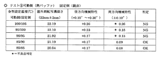
本発明の実施形態について図1ないし図4を参照して説明する。図1は、本実施形態のディスク基板の成形用金型の断面図である。図2は、本実施形態のディスク基板の成形用金型の要部Aの拡大断面図である。図3は、本実施形態のディスク基板の成形用金型による成形時のスタンパの温度を示す仮想グラフ図である。図4は、本実施形態のディスク基板の成形用金型により、成形サイクル時間3.5秒でディスク基板を成形した際の成形テスト結果を示す図表である。図5〜図7は従来技術または比較例による成形テスト結果を示す図表である。 An embodiment of the present invention will be described with reference to FIGS. FIG. 1 is a cross-sectional view of a disk substrate molding die of the present embodiment. FIG. 2 is an enlarged cross-sectional view of a main part A of the disk substrate molding die of the present embodiment. FIG. 3 is a virtual graph showing the temperature of the stamper during molding by the molding die for the disk substrate of the present embodiment. FIG. 4 is a chart showing the molding test results when the disk substrate was molded with a molding cycle time of 3.5 seconds using the disk substrate molding die of the present embodiment. 5 to 7 are charts showing molding test results according to the prior art or comparative examples.
図1に示すように、本発明の一実施形態であるディスク基板の成形用金型はブルーレイ・ディスク(登録商標)用のディスク基板の成形用金型20であり、固定金型21と可動金型31とからなる。固定金型21は、断熱板22を介して図示しない射出成形機の固定盤に取付けられる固定型板23と、固定型板23の断熱板22取付け面の反対面に固定裏板25を介して固着される鏡面板26と、固定型板23、固定裏板25および鏡面板26の中心開口に嵌挿されたゲートインサート29、スプルブッシュ28、およびロケートリングを含む位置決板27と、固定裏板25および鏡面板26の外周端面に嵌挿され固定型板23に固着される固定外周リング24等からなる。鏡面板26は、所定の厚みを有する円筒形部材であり、その裏面側には、ディスク基板を冷却する冷却媒体通路26aが図示しない射出装置側から見て螺旋状に形成されている。またスプルブッシュ28は鏡面板26とは別の冷却媒体通路を流れる冷却媒体により冷却され、ゲートインサート29は、鏡面板26の冷却媒体通路の冷却通路と連通し、主として鏡面板26を流れる冷却媒体により冷却される。
As shown in FIG. 1, a disk substrate molding die according to an embodiment of the present invention is a disk substrate molding die 20 for a Blu-ray Disc (registered trademark), which is a
可動金型31は、可動型板32と、可動型板32の固定金型21側の面に可動裏板33を介して固着される鏡面板34と、鏡面板34の表面に配設されるスタンパ36と、スタンパ36の外周縁部36aを挟持して鏡面板34に保持させる外周スタンパホルダ35と、可動裏板33および鏡面板34の中心開口に遊挿されスタンパ36の内周縁部36bを挟持して鏡面板34に保持させる内周スタンパホルダ38と、内周スタンパホルダ38の内孔を案内し可動型板32に固着される固定スリーブ39と、固定スリーブ39の内孔に嵌挿され軸方向に摺動自在のエジェクタ40と、エジェクタ40の内孔に嵌挿され軸方向に摺動自在のオスカッタ41と、オスカッタ41の内孔に嵌挿され軸方向に摺動自在の突出ピン42と、可動裏板33および鏡面板34の外周端面に嵌挿され可動型板32に固着される可動外周リング43とからなる。鏡面板34は、所定の厚みを有する円筒形部材であり、その裏面側には、ディスク基板を冷却する冷却媒体通路34aが図示しない型締装置側から見て螺旋状に形成されている。これら冷却媒体通路26a,34aには図示しない温調装置から温度調整された冷却媒体が流され鏡面板26,34の温度制御がなされる。ディスク基板の成形用金型20における鏡面板26,34,ゲートインサート29を含む主要部材は、マルテンサイト系のステンレス鋼であるSUS420J2(13Cr−0.3C)(熱膨張率11×10−6/℃)が使用されている。
The
図1および図2に示されるように、固定金型21に対して可動金型31が型合せされた際に形成されるキャビティ37は、スタンパ36の表面44と、固定側の鏡面板26の表面と、外周スタンパホルダ35の内周部と、ゲートインサート29、スプルブッシュ28、内周スタンパホルダ38、固定スリーブ39、エジェクタ40、オスカッタ41および突出ピン42のそれぞれの端面とによって画設されて形成される。そしてスプルブッシュ28に対して図示しない射出装置のノズルを当接させ、該ノズルからスプルブッシュ28の内部通路を介して溶融樹脂がキャビティ37に射出・充填され、冷却固化されることにより、ディスク基板が成形される。本実施形態で成形されるディスク基板は、トラックピッチが0.32μm、板厚1.1mmのブルーレイ・ディスクであり中でも再生専用媒体規格のBD−ROMである。しかし追加型媒体規格のBD−Rや書換可能型媒体規格のBD−REを含む全てのブルーレイ・ディスクを対象とする。しかし他のHD−DVDを含む各種DVD、各種CD等の樹脂から成形されるすべての光ディスクや導光板、光拡散板、レンズ等の他の光学製品をも対象に含むものであってもよい。
As shown in FIGS. 1 and 2, the
本実施形態のスタンパ36は、ニッケル合金を電鋳して製造されたものであり、直径(外径)138mm、内周孔径22mm、板厚が0.3mmとなっている。そしてブルーレイ・ディスク用のスタンパ36の外周縁部36aと内周縁部36bの間の表面44において直径44mm〜118mmの部分には、ディスク基板に対してトラックピッチが0.32μmの微細な凹凸(ドット)を転写するインフォメーションエリア44aが形成されている。そして該インフォメーションエリア44aの内周側の表面には、非インフォメーションエリア44bが形成されている。これらインフォメーションエリア44aの内周側の非インフォメーションエリア44bとの境界44cは、光ディスクの種類により異なる場合が有り得る。またインフォメーションエリアの微細な凹凸も再生専用、追加型、書換可能型等によりドットやグルーブの形状が異なる。スタンパ36に使用されるニッケル合金の熱伝導率は、90W/(m・k)であり、熱膨張率は、12.8×10−6/℃である。なお前記スタンパ36の値は一例であり、例えば板厚は0.2〜0.4mmのものがあり、使用されるニッケルまたはニッケル合金の熱伝導率は、70〜100W/(m・k)程度のものがある。
The
また図2において、詳しく示されるように、鏡面板26,34の表面には金属溶射層を備えた熱緩衝層が形成されている。本実施形態では可動金型31の鏡面板34と固定金型21の鏡面板26とでは、その構成が若干相違するので、まず可動金型31の鏡面板34について説明する。なお本発明において「金属溶射層」とは、「金属(副材料としてセラミックを一定以下含有するものを除外しない)を高温のガス炎やプラズマ環境下に投入して、溶融もしくは半溶融状態の微粒子とし、基体表面に吹き付けることにより形成される皮膜」と定義して使用する。そして前記鏡面板34には、スタンパ36におけるインフォメーションエリア44aと非インフォメーションエリア44bの一部と対向する部分(直径39.5mm)からスタンパ36の外周縁部36aよりやや内側部分に対向する部分にニクロム合金溶射層51を備えた熱緩衝層が形成されている。従って鏡面板34におけるニクロム合金溶射層51の内周縁51bの位置は、スタンパ36および成形されるブルーレイ用ディスク基板の非インフォメーションエリア44bの部分の位置に対向している。なおニクロム合金溶射層51の形成されている部分と形成されていない部分との境界である内周縁51bの位置は、インフォメーションエリア44aと非インフォメーションエリア44bの境界44cであってもよく、前記境界から非インフォメーションエリア44b側に向けて半径4.5mmの範囲内に前記内周縁51bの位置を設けてもよい。なお別の実施形態として、金属溶射層が形成された薄い円筒形の鏡面板の内部に金属溶射層が形成されない薄い円筒形の鏡面板が嵌合されるものでもよい。前記熱緩衝層の形成方法について説明すると、鏡面板34の前記部分は、0.35mmの深さDに切削され、底部に溶射接合面34bが形成されている。なお溶射接合面34bはショットブラスト等の加工をしてもよい。そして前記溶射接合面34bに、厚さ0.3mmのニクロム合金溶射層51が最初に形成され、その表面51aに厚さ0.04mmの硬質クロムメッキ層52が形成されている。そして更にその上層に0.01mmのWc−coコーティング層53が形成されている。なおこれらの表面形成層の厚み等は適宜変更してもよいことは言うまでもない。
As shown in detail in FIG. 2, a heat buffer layer having a metal spray layer is formed on the surface of the
本実施形態においてニクロム合金溶射層51として使用される溶射材料は、metco700(材料型番)であり、Ni20
10W 9Mo 4Cu 1C 1B 1Feからなり、粒子径は125〜16μmのものである。metco700(材料型番)については、熱伝導性が13W/(m・k)程度であり、熱膨張率13.2×10−6/℃程度、硬度HV446〜471である(いずれも常温付近)。しかし溶射材料としては、AMRRY625((材料型番)Ni
21.5Cr 8.5Mo 3Fe 0.5Co)、diamalloy1005((材料型番)Ni 21.5Cr 8.5Mo 3Fe 0.5Co)、diamalloy4004NS((材料型番)Ni
14Cr 9.5Co 5Ti 4Mo 4W 3Al)、diamalloy1006((材料型番)Ni 19Cr 18Fe 3Mo 1Co 1Ti)、AMRRY964((材料型番)Ni
31Cr 11Al 0.6Y)などが用いられる。またNi、Cu、Fe、Al、Mn、C、Siからなる合金であるモネルや、NiにMo、Crを添加したハステロイや、Ni、Cr、Fe、Cu、Moからなる合金であるインコネルやナイモニックなども同様に溶射材料に用いられる。更にはまた、80Ni
20Cr、或いは85Ni 15Crなどのニクロム合金を溶射材料に使用してもよく、それらNi、Crの比率は適宜選択される。また前記材料型番のように、Ni、Crに加え、W、Mo、Co、Ti、Al、B、Si、CTa、Hf、Nb、Zr、Y等を適宜に加えたニクロム合金であってもよく、更に上記以外の組成を含むものを除外しない。これらニクロム合金自体の熱伝導率は、12〜17W/(m・k)程度であり、熱膨張率は9.5〜14×10−6/℃程度である。また溶射材料はCrを含まないかCrが微量でありニクロムの範疇に入らないニッケル基合金であってもよい。これらニクロム合金またはニッケル基合金は、溶射材料として他のセラミック材料や後述するチタン合金等と比較しても廉価である点でも望ましいものである。
In this embodiment, the thermal spray material used as the Nichrome alloy
It consists of 10W 9Mo 4Cu 1C 1B 1Fe and has a particle size of 125-16 μm. With respect to metco700 (material model number), the thermal conductivity is about 13 W / (m · k), the coefficient of thermal expansion is about 13.2 × 10 −6 / ° C., and the hardness is HV446 to 471 (all around normal temperature). However, as a thermal spray material, AMRRY625 ((material model number) Ni
21.5Cr 8.5Mo 3Fe 0.5Co), diaphragm 1005 ((material model) Ni 21.5Cr 8.5Mo 3Fe 0.5Co), diaphragm 4004NS ((material model) Ni
14Cr 9.5Co 5Ti 4Mo 4W 3Al), diamondloy 1006 ((material model number) Ni 19Cr 18Fe 3Mo 1Co 1Ti), AMRRY964 ((material model number) Ni
31Cr 11Al 0.6Y) or the like is used. In addition, Monel, which is an alloy made of Ni, Cu, Fe, Al, Mn, C, Si, Hastelloy made by adding Mo, Cr to Ni, Inconel, Nimonic, which is an alloy made of Ni, Cr, Fe, Cu, Mo Are similarly used for thermal spray materials. Furthermore, 80Ni
Nichrome alloys such as 20Cr or 85Ni 15Cr may be used for the thermal spray material, and the ratio of Ni and Cr is appropriately selected. In addition to Ni and Cr, the material model may be a Nichrome alloy appropriately added with W, Mo, Co, Ti, Al, B, Si, CTa, Hf, Nb, Zr, Y, etc. Further, those containing other compositions than the above are not excluded. These nichrome alloys themselves have a thermal conductivity of about 12 to 17 W / (m · k), and a thermal expansion coefficient of about 9.5 to 14 × 10 −6 / ° C. Further, the thermal spray material may be a nickel-based alloy that does not contain Cr or that has a very small amount of Cr and does not fall within the category of nichrome. These nichrome alloys or nickel-base alloys are desirable because they are inexpensive as compared with other ceramic materials or titanium alloys described later as the thermal spray material.
更に金属溶射材料としては、ニクロム合金以外に、チタン合金、ジルコニウム合金、クロム合金などを用いても良い。またステンレスであっても鏡面板34を形成するステンレス鋼(SUS420J2)の熱伝導率よりも熱伝導率の低いステンレスを金属溶射材料としてもよい。さらには本発明においてはサーメット材の溶射を除外するものではないが、金属との接合性に優れ、かつ熱膨張率がステンレス鋼とさほど相違しないものが望ましく、耐衝撃性が劣るものは除かれる。したがって炭化物、窒化物、酸化物からなるセラミック材料の比率が一定以下(40wt%より少なく、望ましくは30wt%以下)であることが望ましい。ただし金属材料のみからなる溶射材料と比較すると、セラミック材料を含むものは、金属との接合性(親和性)に劣る上に高額なのでステンレス鋼よりも熱伝導率が低い金属のみからなる溶射材料がより望ましいと言える。
Furthermore, as the metal spray material, a titanium alloy, a zirconium alloy, a chromium alloy, or the like may be used in addition to the nichrome alloy. Moreover, even if it is stainless steel, it is good also considering the stainless steel (SUS420J2) which forms the
金属溶射層を構成する金属材料(バルク材)の熱伝導率は、鏡面板34を形成するステンレス鋼(SUS420J2)の熱伝導率である21W/(m・k)と比較して熱伝導率が低いものが使用される。しかし本発明では鏡面板34の冷却媒体通路34aを流れる冷却媒体による冷却が溶融樹脂に及ぶ際には良好な熱伝導性が必要とされるから、あまりに熱伝導率が低すぎる(例えば4W/(m・k)以下)のものを使用すると、断熱性と熱伝導性の両立ができない。具体的には金属溶射層を構成する金属の熱伝導率が10〜21W/(m・k)のものが望ましく、更には10〜16W/(m・k)のものがより望ましい。またこれらの熱伝導率の金属材料を使用すると金属溶射層の厚さを一定以上厚く(例えば150μm以上)することができ、耐久性の点でも望ましい。
The thermal conductivity of the metal material (bulk material) constituting the metal sprayed layer is higher than that of 21 W / (m · k), which is the thermal conductivity of stainless steel (SUS420J2) forming the
気孔を有する金属溶射層全体の熱伝導率については、「溶射技術マニュアル」編著者:馬込正勝に次のような記載がなされている。
すなわち熱伝導率kは、次の実験式で表わすことができる。
k≒kc(1−βP)
Kc=バルク材の熱伝導率
P=気孔率(%)
β=物質と材料の微細組織による因子を示す。
また同著によれば、銅、アルミニウムにおける鋳造材と溶線式フレーム溶射皮膜を比較したところ、同一金属でも溶射皮膜では熱伝導率が50%以下となる実例(表)が示されている。
本発明においても前記金属溶射層には、後述するように一部例外を除き0.5〜10%の空孔率を有するような金属溶射層を形成する場合が想定されているから、実際の気孔を有する金属溶射層全体では、金属材料(バルク材)の50%程度の熱伝導率となっていることが想定される。従って本実施形態に使用されるニクロム合金の熱伝導率が13W/(m・k)であっても、気孔を有する金属溶射層自体の熱伝導率は、13W/(m・k)以下、例えば5〜13W/(m・k)となっていることが想定される。
About the thermal conductivity of the whole metal sprayed layer which has a pore, the following description is made | formed by "The thermal spraying technique manual" author: Masakazu Magome.
That is, the thermal conductivity k can be expressed by the following empirical formula.
k≈kc (1-βP)
Kc = thermal conductivity of bulk material P = porosity (%)
β = factor due to the microstructure of the substance and material.
According to the same book, a comparison between a cast material of copper and aluminum and a hot wire flame sprayed coating shows an example (table) in which the thermal conductivity of the same metal is 50% or less.
In the present invention, the metal sprayed layer is assumed to form a metal sprayed layer having a porosity of 0.5 to 10% with some exceptions as described later. It is assumed that the entire metal sprayed layer having pores has a thermal conductivity of about 50% of the metal material (bulk material). Therefore, even if the thermal conductivity of the nichrome alloy used in this embodiment is 13 W / (m · k), the thermal conductivity of the metal sprayed layer itself having pores is 13 W / (m · k) or less, for example, It is assumed that it is 5 to 13 W / (m · k).
金属溶射層の熱膨張率は、主として鏡面板34を構成する金属と熱膨張率と大きく相違しないことが金属溶射層の剥離を防止する上で望ましい。具体的には、主として鏡面板34を構成するステンレス鋼(SUS420J2)の熱膨張率は、11.5×10⁻⁶/℃であり、他に鏡面板として使用される可能性があるステンレス鋼の熱膨張率も11×10−6/℃〜17×10−6/℃程度であるから、金属溶射層の熱膨張率も9.5×10−6/℃〜18×10−6/℃であることが望ましい。
It is desirable that the thermal expansion coefficient of the metal spray layer is not largely different from that of the metal constituting the
金属溶射層の硬度は、主として鏡面板34を構成するステンレス鋼(SUS420J2)の硬度(500〜520HV)よりは若干劣っても400HV以上であれば十分であり、ニッケル基合金の溶射層の硬度は通常450HV前後である。またWc−coコーティングは硬度2000HV程度であるから、これら硬質部材による表面処理を行う場合は、金属溶射層の硬度がステンレス鋼の硬度よりも若干低いことはより一層問題とならない。従って本発明の金属溶射層は、従来技術の熱緩衝層と比較して、成形時に発生する諸問題に対して耐久性が高いと言える。
The hardness of the metal-sprayed layer is 400 HV or more even if it is slightly inferior to the hardness (500 to 520 HV) of the stainless steel (SUS420J2) constituting the
ニクロム合金(metco700)の溶射方法は、プラズマ溶射によって行われる。本実施形態では、噴射点温度1300℃、噴射装置内温度(粒子温度)2000℃、ワーク温度150℃でmetco700の溶射が鏡面板34に切削された溶射接合面34bに対して行われる。そしてプラズマ溶射により溶射された金属溶射層の空孔率は、0.5〜8%である。しかし本発明では金属溶射層により熱緩衝層を形成するので、断熱作用を有するように空孔率が高い方が望ましく、空孔率が2%以上とすることがより望ましい。そして空孔の大きさおよび粒子径は前記材料径にほぼ一致し125〜16μmのものがほとんどとなっている。ただし溶射距離の変更等の溶射状態の変更により空孔率を変化させることもできる。また溶射層の形成としては粉末式フレーム溶射、アーク溶射といった空孔率が高くなる溶射方法を用いて空孔率5〜10%の金属溶射層を形成することができる。また前記metco700よりも更に熱伝導率が低い溶射材料を使用する際は、前記プラズマ溶射や高速フレーム溶射により空孔率を0〜2%程度としてもよい。また空孔を有する金属溶射層を形成後、空孔部分に他の断熱性の高い部材を含浸させるようにしてもよい。
Nichrome alloy (metco 700) is sprayed by plasma spraying. In the present embodiment, the thermal spraying of metco 700 is performed on the thermal
プラズマ溶射による金属溶射層の形成作業は、鏡面板34の溶射接合面34bに対して当初、0.5〜0.8mm程度の厚みにニクロム合金溶射層の形成を行う。そして前記ニクロム合金溶射層を研磨により薄くしていって0.3mmのニクロム合金溶射層51を形成する。当初は最終的に必要とされるニクロム合金溶射層51の厚みよりも厚く溶射し、その後研磨を行う理由は、溶射を行ったままの表面は、凹凸が目立つので、研磨加工によって表面51aを鏡面状態にするためである。なおニクロム合金溶射層51の厚みは、0.15〜0.4mmが適切な厚みである。なお従来のジルコニアやTinのみの加工においては、表面の研磨加工を行うことが極めて難しかったが本発明ではそのような問題はなくなり、また再溶射による再加工も容易となった。本実施形態では更に平坦な面を得るためと強度アップのために、表面形成層として硬質クロムメッキ層52が厚さ0.001〜0.05mmの厚さに平滑形成されている。硬質クロムメッキ層52は、熱伝導率93.7W/(m・k)、熱膨張率17×10−6/℃であり、前記ニクロム合金溶射層51と熱膨張率が近く、接合性(親和性)が高い。また硬質クロムメッキ層52は、硬度が850〜1000HVであり、ニクロム合金溶射層51の保護に有用である。硬質クロムメッキ層52も前記ニクロム合金溶射層51と同じく、適宜金属配合を変化させてもよく、ニッケルリンメッキやより親和性の高いニクロム合金メッキとしてもよい。
In forming the metal sprayed layer by plasma spraying, a nichrome alloy sprayed layer is initially formed with a thickness of about 0.5 to 0.8 mm on the sprayed
本実施形態では表面形成層は、厚さ0.04mmの硬質クロムメッキ層52の上層に更に耐磨耗性を高め平滑性を得る目的から厚さ0.01mmのWc−coコーティング層53(熱伝導率60W/(m・k))が積層形成されている。またWc−coコーティング層53による耐磨耗層については、DLCなど適宜の耐摩耗層への変更が可能である。なお本発明において表面形成層は形成せずに、ニクロム合金溶射層51を鏡面加工したのみで鏡面板34の表面を形成してもよいし、表面形成層として、硬質クロムメッキ層52のみ、またはWc−coコーティング層53のみを形成してもよい。従って本発明において鏡面板34に表面形成層が設けられる場合、熱緩衝層であるニクロム合金溶射層51は、鏡面板34の表面には形成されず、表面と冷却媒体通路34aの間に形成される。
In the present embodiment, the surface forming layer is a 0.01 mm thick Wc-co coating layer 53 (thermal layer) for the purpose of further improving wear resistance and smoothness on the upper layer of the hard
次に図1、図2により固定金型21の鏡面板26の表面に形成される熱緩衝層について説明する。鏡面板26の内周孔26cの直径は、39.5mmとなっている。また鏡面板26の表面側の外周側の直径は、成形品が収縮した際に直径120mmとなる直径(120.08mm)となっている。そして前記鏡面板26の表面には、ゲートインサート29に隣接する内周側部分と、外周側から僅かに内側の119mmの部分までの間の部分に、熱緩衝作用を有する金属溶射層としてニクロム合金溶射層61が形成されている。鏡面板26の外周縁の部分にニクロム合金溶射層61を設けないのは、鏡面板26の外周は、型開閉の際に外周スタンパホルダ35内に嵌合されるので、接触等によって熱緩衝層が剥離するのを防止するためである。よって鏡面板26の表面においてはほぼ全面がニクロム合金溶射層61となっており、ゲートインサート29にはニクロム合金溶射層は形成されていない。そして固定金型21の鏡面板26の前記ニクロム合金溶射層61と可動金型31の鏡面板34の前記ニクロム合金溶射層51は対向して形成され、その内周縁61bの位置は、ニクロム合金溶射層51の内周縁51bの位置と略一致して対向して形成されている。なお、鏡面板26における熱緩衝層の内周縁61bの位置は、前記の直径39.5mmに4.5mmを加えた範囲まで拡大され、その内側部分には熱緩衝層が形成されていないものでもよい。更には鏡面板の内周孔をもっと小さくして39.5mmから4.5mmを減算した範囲まで熱緩衝層を設けてもよい。従って鏡面板26のニクロム合金溶射層61における内周縁61bの位置と、可動金型31の鏡面板34のニクロム合金溶射層51における内周縁51bの位置とは、直径9mmまでの範囲において、いずれか一方が大きいものまでが許容される。
Next, the heat buffer layer formed on the surface of the
鏡面板26の表面は、0.34mmの深さDに切削され、底部に溶射接合面26bが形成されている。なお溶射接合面26bはショットブラスト等の加工をしてもよい。そして前記溶射接合面26bに、厚さ0.3mmのニクロム合金溶射層61が最初に形成されている。ニクロム合金溶射層61の溶射方法や材質等は、可動金型31の鏡面板34のものと同じである。そして前記ニクロム溶射層61の表面61aに、厚さ0.04mmの硬質クロムメッキ層62が形成されている。そして硬質クロムメッキ62の表面がキャビティ形成面62aとなっており、Wc−coコーティング層53は形成されていない。なお硬質クロムメッキ層62の表面は、Wc−coコーティング層53と比較すると、滑らかでなく僅かな凹凸はあるが、スタンパ36を取付けるものでないからスタンパ36の寿命等を考慮する必要がなく、ブルーレイ・ディスクにおいて、固定金型21の鏡面板26によって成形される部分は、レーベル面でありレーザー光の読取りに関係ないので高い精度は要求されない。また成形されたブルーレイ用ディスク基板の離型の際には僅かな凹凸があった方がかえって離型性に優れる。そしてこれらの表面形成層の厚み等は適宜変更してもよいことは言うまでもない。
The surface of the
次に図1、図3、図4によりブルーレイ用ディスク基板の成形方法について記載する。
また同時に、図3の本実施形態のブルーレイ用ディスク基板の成形用金型20による成形時のスタンパ36の温度を示す仮想グラフ図を用いて、熱緩衝層の目的について説明する。まず型開されブルーレイ用ディスク基板が取出されたディスク基板の成形用金型20のスタンパ36は、鏡面板34からの冷却と空気に晒されて、成形サイクル中で最も温度が低下した状態にある。本実施形態ではスタンパ36の温度は、90℃程度となっている。そして図示しない射出成形機の型締装置により可動金型31を移動させ、固定金型21に対して可動金型31を型合せし、キャビティ37を形成する。次に図示しない射出装置のノズルから計量時に320℃ないし395℃の溶融されたポリカーボネート樹脂をスプルブッシュ28を介してキャビティ37内へ射出する。なお図4等のテストにも用いられる本実施形態の例では、前記射出装置の加熱筒前部の設定温度は370℃、ノズル温度は320℃に設定されている。キャビティ37内に射出された溶融樹脂は、スタンパ36の表面に沿って外周に向けて流動され、厚さ0.3mmのニッケル合金製スタンパ36を急速に加熱する。
Next, a method for forming a Blu-ray disc substrate will be described with reference to FIGS.
At the same time, the purpose of the thermal buffer layer will be described with reference to a virtual graph showing the temperature of the
その際スタンパ36を昇温させた熱は、スタンパ36裏面側の極めて薄いWc−coコーティング層53、硬質クロムメッキ層52を介して、ニクロム合金溶射層51に伝えられる。また同様に固定金型21側も硬質クロムメッキ層62とニクロム合金溶射層61を介して、鏡面板26のステンレス鋼に溶融樹脂の熱が伝えられる。しかし前記のようにニクロム合金の熱伝導率は、13W/(m・k)と鏡面板26,34を形成するステンレス鋼の熱伝導率よりも低い。それに加えてニクロム合金溶射層51,61は、容積比において0.5〜8%の空孔率を有しているので、前記空気層の存在によってバルク材であるニクロム合金の熱伝導率より更に熱伝導率が低くなっており、熱遮蔽効果を有する。
At this time, the heat that has raised the temperature of the
従来技術(熱緩衝層なし)では、射出充填された溶融樹脂がスタンパに当接されスタンパが昇温されても、その熱は裏面側の鏡面板に奪われ、急速にスタンパが昇温されなかった。しかし本発明では、ニクロム合金溶射層51による熱遮蔽効果によりスタンパ36は急速に昇温される。そして射出開始と同時か僅かに遅れて、型締装置により可動金型31を固定金型21側に型締移動させ、0.2秒程度、例えば350〜400kNの高型締力を及ぼして射出圧縮成形が行われる。その際の高型締力によってスタンパ36のインフォメーションエリア44aの微細な凹凸がブルーレイ用ディスク基板側により良好に転写される。そのような高型締力を及ぼすことを可能とすることは、熱緩衝層として金属溶射層が形成されているからである。従って金属溶射層による熱緩衝層が形成されたディスク基板の成形用金型20は、従来のセラミック材の熱緩衝層のディスク基板の成形用金型よりも高型締力による成形を長期間に亘って行うことができ長寿命である。そして型締力を及ぼした際には前記のようにスタンパ36が急速に昇温されているから、溶融樹脂の冷却が遅れ、良好な転写が行われる。
In the prior art (no thermal buffer layer), even if the molten resin injected and filled comes into contact with the stamper and the temperature of the stamper is raised, the heat is taken away by the mirror plate on the back side and the temperature of the stamper is not raised rapidly. It was. However, in the present invention, the temperature of the
また鏡面板34の冷却媒体通路34aには冷却媒体が流通されているから、鏡面板34側からスタンパ36を介してブルーレイ用ディスク基板となる溶融樹脂に対して冷却が行われる。しかし本実施形態では、従来技術と比較して転写時のみにスタンパ36の温度を溶融樹脂の熱により高温にすることができることから、鏡面板34の温度設定を、従来よりも低く設定しても、従来と同じ溝深さの成形を行うことが可能である。
Further, since the cooling medium is circulated through the cooling
また本実施形態では、鏡面板34の表面のうち、スタンパ36のインフォメーションエリア44aよりも内側の非インフォメーションエリア44bに対向する部分と、型閉された際に、前記非インフォメーションエリア44bに向かい合って対向する固定金型21のゲートインサート29の表面のキャビティ形成面29bには、ニクロム合金溶射層51,61が形成されていないことから、その部分については、キャビティ37内の溶融樹脂の冷却をより早めることができる。そしてキャビティ37内の溶融樹脂の冷却中にゲートカットが行われる。ゲートカットに際しては、可動金型31に配設されたオスカッタ41が、固定金型21に配設されたゲートインサート29のメスカッタ29a内に向けて前進され、オスカッタ41がメスカッタ29a内に嵌合される。そしてゲートカットが行われると可動金型31および固定金型21からディスク基板に離型エアを噴出させながら、可動金型31を移動させ、型開きを行い、ディスク基板の取出しを行う。その際に従来よりも鏡面板34の温度を低下またはゲートインサート29を冷却する温度を低下させることができるから、成形サイクル時間を早くすることができる。そして取出し時におけるディスク基板の非インフォメーションエリア44bとは反対側の面の温度についても従来よりも低温で溶融樹脂の冷却固化も進行している。よって取出機を比較的安価な強く吸盤が当接されるタイプのものを使用しても、非インフォメーションエリアの冷却固化が進行したブルーレイ用ディスク基板を変形なしに取出すことができる。その結果、製品であるブルーレイ・ディスクを再生機(デッキ)で再生する際に、非インフォメーションエリアを装置内で押えて回転させるが、ブルーレイ・ディスクの特に外周側の波打をより小さくして回転させることができる。なお型開中に鏡面板34に取付けられたスタンパ36の表面は更に冷却され、次に射出開始されるまでにスタンパ36の温度は90℃程度まで降温される。一方成形されたブルーレイ用ディスク基板は、詳細は省略するが公知の蒸着やコーティング等の各工程を経て、ブルーレイ・ディスクに製造される。
Further, in the present embodiment, a portion of the surface of the
次に実際に、本実施形態のディスク基板の成形用金型20、従来技術の成形用金型、比較例の成形用金型を用いて、ブルーレイ・ディスク(BD−ROM)を成形した際のテスト結果に基づいて説明をする。図4は、本実施形態のディスク基板の成形用金型20により、成形サイクル時間3.5秒でディスク基板を成形した際の成形テスト結果を示す図表である。本実施形態のディスク基板の成形方法の特徴は、可動金型31の鏡面板34、固定金型21の鏡面板26を冷却する冷却媒体である水の温度(温調器による制御温度)を略一致させることである。なお、ただしこの場合の略一致とは、同温または3℃までの温度差(より望ましくは2℃までの温度差)を許容するものとする。鏡面板26,34の温度を略一致させることにより、成形されるディスク基板の径方向機械特性(Radius
Deviation)と、周方向機械特性(Tangential Deviation)を良品と判定される値を得ることができる。また本実施形態では、図4に示されるように、鏡面板26,34へ送られる冷却媒体の温度を80℃〜95℃の範囲でテストした際に、すべての条件をクリアする良好な結果が得られた。各条件項目について更に説明すると、成形されるブルーレイ用ディスク基板の最外周転写溝深さ(良品と判定される範囲:22nm±2nm)については、80℃〜100℃のすべての範囲で良品と判定される値が得られたが、その中でも95℃において最も良好な値が得られ、低温になるにつれて良品と判定される値内ではあるが値が低下した。従ってディスク基板の溝形状の幅が小さく溶融樹脂が入りにくい場合や、直角方向に深い溝形状が要求される場合は、冷却媒体の温度を高くすることが望ましく、予期値としては成形サイクル時間を延ばせば100℃まで高温化させることにより対応できる。また今回は、いずれも3.5秒の成形サイクル時間で成形を行ったが、成形サイクル時間を更に短縮したい場合は、冷却媒体の温度を実験値では80℃、予期値としては75℃まで低温化させることにより対応できる。
Next, when the Blu-ray disc (BD-ROM) was actually molded using the disk substrate molding die 20 of the present embodiment, the conventional molding die, and the comparative molding die. The explanation is based on the test results. FIG. 4 is a chart showing a molding test result when the disk substrate was molded with a molding cycle time of 3.5 seconds by the disk substrate molding die 20 of the present embodiment. A feature of the disk substrate molding method of this embodiment is that the temperature of water (control temperature by a temperature controller) that is a cooling medium for cooling the
It is possible to obtain a value that determines that the device is a non-defective product and the circumferential mechanical property (Tangential Deviation). Moreover, in this embodiment, as shown in FIG. 4, when the temperature of the cooling medium sent to the
またブルーレイ用ディスク基板の径方向機械特性(良品と判定される範囲:+0.10°〜+0.30°)については、転写面の中心側が突出し外周側に向けて下降するように成形することが後工程との関係において望ましく、80℃〜100℃のすべての範囲で良品と判定される値が得られたが、その中でも85℃〜95℃の範囲で最も良好な値が得られた。更に周方向機械特性(良品と判定される範囲:±0.10°)については、ブルーレイ用ディスク基板のうねりに関するものであり値が小さいほど望ましいが、80℃〜95℃の範囲で良品と判定される値が得られ、とりわけ80℃と冷却媒体の温度が低温な場合ほど良好な値が得られた。しかし成形サイクル時間を延長すれば、更に100℃まで良品が得られることが経験則から予期された。 In addition, regarding the radial direction mechanical characteristics of the Blu-ray disc substrate (range to be judged as non-defective product: + 0.10 ° to + 0.30 °), the center side of the transfer surface protrudes and descends toward the outer peripheral side. Desirable in relation to the post-process, a value determined to be a non-defective product was obtained in the entire range of 80 ° C. to 100 ° C. Among them, the best value was obtained in the range of 85 ° C. to 95 ° C. Further, the circumferential mechanical characteristics (range to be judged as non-defective product: ± 0.10 °) are related to the waviness of the disc substrate for Blu-ray, and the smaller the value, the better, but it is judged to be non-defective in the range of 80 ° C to 95 ° C. In particular, when the temperature of the cooling medium is as low as 80 ° C., a better value was obtained. However, it was expected from experience that if the molding cycle time is extended, good products can be obtained up to 100 ° C.
次に図5〜図7により従来技術および比較例について説明する。図5は、従来の鏡面板に熱緩衝層が形成されていないディスク基板の成形用金型により、成形サイクル時間3.5秒でブルーレイ用ディスク基板を成形した際の成形テスト結果を示す図表である。ディスク基板の径方向機械特性を良好に保つため、固定金型および可動金型の鏡面板に送る冷却媒体の温度は一致させている。図5の例ではスタンパの表面温度を低下させないために、冷却媒体の温度を90℃以上としないと、最外周転写溝深さが、良品と判定される値が得られなかった。しかし温度が100℃の場合では周方向機械特性が不良と判定される値となり、冷却媒体の温度が95℃の場合のみブルーレイ用ディスク基板が良品のものが成形でき、成形できる冷却媒体の温度の範囲が狭かった。また良品と判定される値内であっても最外周転写溝深さの値は、低めのものであった。そして冷却媒体の温度が95℃以下の温度での成形に失敗していることから、今後成形サイクル時間の短縮の可能性が少ないものであった。 Next, the prior art and the comparative example will be described with reference to FIGS. FIG. 5 is a chart showing the results of a molding test performed when a Blu-ray disc substrate was molded with a molding cycle time of 3.5 seconds using a conventional mold for molding a disc substrate on which no heat buffer layer was formed on the mirror surface plate. is there. In order to keep the radial mechanical characteristics of the disk substrate in good condition, the temperature of the cooling medium sent to the mirror plate of the fixed mold and the movable mold is matched. In the example of FIG. 5, in order not to lower the surface temperature of the stamper, unless the temperature of the cooling medium is set to 90 ° C. or higher, a value for determining the outermost transfer groove depth as a non-defective product could not be obtained. However, when the temperature is 100 ° C., the circumferential mechanical characteristics are determined to be poor. Only when the cooling medium temperature is 95 ° C., the Blu-ray disc substrate can be molded, and the temperature of the cooling medium that can be molded is The range was narrow. Even within the value determined to be non-defective, the outermost transfer groove depth value was low. Since the molding of the cooling medium at a temperature of 95 ° C. or lower has failed, there is little possibility of shortening the molding cycle time in the future.
図6は、スタンパが配設された可動金型の鏡面板のみに熱緩衝層が形成され、スタンパが配設されていない固定金型の鏡面板に熱緩衝層が形成されていないディスク基板の成形用金型により、固定金型および可動金型の鏡面板に送る冷却媒体の温度は一致させて、成形サイクル時間3.5秒でブルーレイ用ディスク基板を成形した際の成形テスト結果を示す図表である。図5の例では、最外周転写溝深さは、本実施形態である図4の例と同じく良好な値が得られたが、径方向機械特性において、すべての冷却媒体の温度において、ブルーレイ用ディスクの良品と判定される値が満足できないという結果となった。これは可動金型の鏡面板(スタンパ有り)には熱緩衝層があるために冷却が遅れるのに対し、固定金型側の鏡面板には熱緩衝層がないために冷却が進行し、転写面の中心側が凹部となる逆反りが発生するからである。また周方向機械特性も冷却媒体の温度が90℃以上の場合に不良品と判定される値となった。 FIG. 6 shows a disk substrate in which a heat buffer layer is formed only on a mirror plate of a movable mold provided with a stamper, and no heat buffer layer is formed on a mirror plate of a fixed mold without a stamper. Chart showing the results of the molding test when molding the Blu-ray disc substrate with a molding cycle time of 3.5 seconds with the molding die matched to the temperature of the cooling medium sent to the mirror plate of the fixed mold and movable mold. It is. In the example of FIG. 5, the outermost transfer groove depth was as good as that of the example of FIG. 4 of the present embodiment. However, in the radial direction mechanical characteristics, for all the temperatures of the cooling medium, As a result, the value judged to be a good disc was not satisfied. This is because the mirror plate of the movable mold (with the stamper) has a thermal buffer layer, so cooling is delayed, whereas the mirror plate on the fixed mold side has no thermal buffer layer, so cooling proceeds and the transfer proceeds. This is because a reverse warp occurs in which the center side of the surface becomes a recess. Further, the circumferential direction mechanical characteristics were also determined to be defective when the temperature of the cooling medium was 90 ° C. or higher.
図7は、スタンパが配設された可動金型の鏡面板のみに熱緩衝層が形成され、スタンパが配設されていない固定金型の鏡面板に熱緩衝層が形成されていないディスク基板の成形用金型(図6と同じ金型)により、固定金型の鏡面板に送る冷却媒体の温度を可動金型の鏡面板に送る冷却媒体の温度よりも5℃高くし、成形サイクル時間3.5秒でブルーレイ用ディスク基板を成形した際の成形テスト結果を示す図表である。図7の例では、最外周転写溝深さは、本実施形態である図4の例と同じく良好な値が得られた。また径方向機械特性においても、図4の例と同じく良好な値が得られた。しかし周方向機械特性において、可動金型側の冷却媒体の温度が90℃以上の場合にブルーレイ用ディスクの良品と判定される値が得られないという結果となった。これは型開の際の固定金型の温度が可動金型の温度と比較して高いためで、ブルーレイ用ディスク基板の転写面と反対側の冷却固化が遅れ、その結果、固定金型から離型されにくくなるため、うねりが発生するからである。また可動金型の温度が低温域の場合しか良品と判定されるブルーレイ用ディスク基板が得られないので、良品と判定されるものであっても最外周転写溝深さの値は、低めのものしか得られなかった。
FIG. 7 shows a disk substrate in which a heat buffer layer is formed only on a mirror plate of a movable mold provided with a stamper, and no heat buffer layer is formed on a mirror plate of a fixed mold without a stamper. The temperature of the cooling medium sent to the mirror plate of the fixed mold is made 5 ° C. higher than the temperature of the cooling medium sent to the mirror plate of the movable mold by the molding die (the same mold as FIG. 6), and the
従来技術および比較例と較べた上記の結果から明らかなように、本実施形態のスタンパ36が配設された可動金型31の鏡面板34と、スタンパが配設されていない固定金型21の鏡面板26の両方に熱緩衝層であるニクロム合金溶射層51,61が形成されたディスク基板の成形用金型20は、良品と判定されるブルーレイ用ディスクを成形可能な冷却媒体の温度域が広い。従って成形条件設定の際に、更に転写が良好なものを追求したり、成形サイクル時間を短縮したりする選択の幅の広いものである。
As is clear from the above results compared with the prior art and the comparative example, the
また本発明については、一々列挙はしないが、上記した本実施形態のものに限定されず、当業者が本発明の趣旨を踏まえて変更を加えたものについても、適用されることは言うまでもないことである。本実施形態では可動金型31の鏡面板34にスタンパ36が配設されており、固定金型21の鏡面板26にはスタンパが配設されていないが、固定金型の鏡面板にスタンパが配設され、可動金型の鏡面板にスタンパが配設されないものであってもよい。また固定金型または両方の金型にスタンパが配設され、両方の鏡面板に金属溶射層が形成されたものであってもよい。また金属溶射層が設けられる部分は転写領域に対向する部分のみに限定されず、スタンパ裏面に対向する全面としてもよく、更には金属溶射層の厚みについて、冷却媒体通路と対向する部分とそうでない部分について変化をつけてもよい。更に鏡面板は、複層構成にして、例えば第一層に冷却媒体通路を形成し、第二層に金属溶射層を形成してもよい。また本発明は、ディスク基板の成形に限定されず、鏡面板に取付けられたスタンパの微細な凹凸を転写する導光板、光拡散板、レンズ等の光学製品の射出成形、射出圧縮成形、射出プレスにも用いることができる。
The present invention is not enumerated one by one, but is not limited to the one in the above-described embodiment, and it goes without saying that the present invention is applied to those modified by a person skilled in the art based on the gist of the present invention. It is. In this embodiment, the
20 ディスク基板の成形用金型
21 固定金型
26,34 鏡面板
26a,34a 冷却媒体通路
31 可動金型
36 スタンパ
37 キャビティ
51,61 ニクロム合金溶射層
51b,61b 内周縁
52,62 硬質クロムメッキ層
20 Mold for molding a
Claims (4)
前記金型のキャビティ表面またはキャビティ表面と冷却媒体通路との間には、ニクロム合金からなり、0.5〜10%の空孔率の金属溶射層が形成されていることを特徴とする光学製品の成形用金型。 In a mold for optical products in which a cavity is formed when a fixed mold and a movable mold are combined, and a molded product is molded by one of injection molding, injection compression molding, and injection press.
An optical product comprising a cavity surface of the mold or between the cavity surface and a cooling medium passage, a metal sprayed layer made of a nichrome alloy and having a porosity of 0.5 to 10%. Mold for molding.
A molten resin is injected and filled into a cavity of a molding die for an optical product according to claim 1, and the molten resin is cooled and solidified through the metal sprayed layer by a cooling medium flowing through the cooling medium passage. A method for molding an optical product.
Priority Applications (1)
| Application Number | Priority Date | Filing Date | Title |
|---|---|---|---|
| JP2007018011A JP4789818B2 (en) | 2007-01-29 | 2007-01-29 | Mold for molding optical product and method for molding optical product |
Applications Claiming Priority (1)
| Application Number | Priority Date | Filing Date | Title |
|---|---|---|---|
| JP2007018011A JP4789818B2 (en) | 2007-01-29 | 2007-01-29 | Mold for molding optical product and method for molding optical product |
Publications (3)
| Publication Number | Publication Date |
|---|---|
| JP2008183765A JP2008183765A (en) | 2008-08-14 |
| JP2008183765A5 JP2008183765A5 (en) | 2009-02-19 |
| JP4789818B2 true JP4789818B2 (en) | 2011-10-12 |
Family
ID=39727109
Family Applications (1)
| Application Number | Title | Priority Date | Filing Date |
|---|---|---|---|
| JP2007018011A Expired - Fee Related JP4789818B2 (en) | 2007-01-29 | 2007-01-29 | Mold for molding optical product and method for molding optical product |
Country Status (1)
| Country | Link |
|---|---|
| JP (1) | JP4789818B2 (en) |
Families Citing this family (3)
| Publication number | Priority date | Publication date | Assignee | Title |
|---|---|---|---|---|
| JP5234640B2 (en) * | 2009-02-02 | 2013-07-10 | 株式会社名機製作所 | Ultra-thin light guide plate molding die and molding method |
| JP6496578B2 (en) * | 2015-03-12 | 2019-04-03 | 株式会社リケン | piston ring |
| JP6418619B1 (en) * | 2017-10-19 | 2018-11-07 | トーノファインプレーティング株式会社 | Mold, mold manufacturing method, resin molding apparatus and molded product molding method |
Family Cites Families (10)
| Publication number | Priority date | Publication date | Assignee | Title |
|---|---|---|---|---|
| JPH04223537A (en) * | 1990-12-26 | 1992-08-13 | Nec Eng Ltd | Image file storing system |
| JPH0551724A (en) * | 1991-08-23 | 1993-03-02 | Toyota Motor Corp | Formation of porous sprayed layer |
| JPH1134112A (en) * | 1997-07-11 | 1999-02-09 | Toshiba Mach Co Ltd | Precise mold |
| JPH11156897A (en) * | 1997-11-28 | 1999-06-15 | Hitachi Maxell Ltd | Mold for injecting molding of optical disk board, and molding board |
| JPH11311498A (en) * | 1998-04-28 | 1999-11-09 | Kyocera Corp | Heat transmitting tube for heat exchanger |
| JP3890768B2 (en) * | 1998-09-22 | 2007-03-07 | 旭硝子株式会社 | Pressure reducing device for vacuum degassing system |
| JP2004181716A (en) * | 2002-12-02 | 2004-07-02 | Matsushita Electric Ind Co Ltd | Mold for injection molding optical disk |
| CN100351064C (en) * | 2003-03-03 | 2007-11-28 | 松下电器产业株式会社 | Die for molding disk substrate and method of manufacturing disk substrate |
| JP4780932B2 (en) * | 2004-05-25 | 2011-09-28 | 京セラ株式会社 | Corrosion-resistant member, method for manufacturing the same, and member for semiconductor / liquid crystal manufacturing apparatus |
| JP2008127614A (en) * | 2006-11-20 | 2008-06-05 | Mitsubishi Engineering Plastics Corp | Thermal spray coating structure, and insert |
-
2007
- 2007-01-29 JP JP2007018011A patent/JP4789818B2/en not_active Expired - Fee Related
Also Published As
| Publication number | Publication date |
|---|---|
| JP2008183765A (en) | 2008-08-14 |
Similar Documents
| Publication | Publication Date | Title |
|---|---|---|
| JP4223537B2 (en) | Mold for molding disk substrate, mirror plate thereof, method for molding disk substrate, and disk substrate | |
| JP4181017B2 (en) | Mold for molding | |
| JPWO2007020769A1 (en) | Optical element molding die and method for manufacturing the same | |
| JP4789818B2 (en) | Mold for molding optical product and method for molding optical product | |
| JP3747983B2 (en) | Molding method of molded product and mold assembly | |
| JP2008183765A5 (en) | ||
| JP4197183B2 (en) | Disk substrate molding die and disk substrate manufacturing method | |
| JP5234640B2 (en) | Ultra-thin light guide plate molding die and molding method | |
| JP2008168646A (en) | Molding process of optical element | |
| JPWO2011030523A1 (en) | Disc substrate molding apparatus, disc substrate molding method, and disc substrate molding die | |
| JP4769654B2 (en) | Blu-ray Disc manufacturing method | |
| JP2003320552A (en) | Mold assembly for molding optical disk | |
| JP2004195756A (en) | Mold for optical disk substrate | |
| JPH1134112A (en) | Precise mold | |
| JP3695400B2 (en) | Mold device for optical disc molding | |
| JP2009051138A (en) | Mold and method for manufacturing the same | |
| JP3888580B2 (en) | Method of manufacturing substrate for recording medium and injection molding apparatus | |
| JP2007001272A (en) | Mold apparatus, optical disc substrate, manufacturing method of optical disc substrate and multi layered insulating stamper | |
| JPH11291292A (en) | Molding die | |
| JP2009242141A (en) | Regenerating method of mold and regenerated mold | |
| JPH0336011A (en) | Die for high frequency heating | |
| JP2000094480A (en) | Molding die and injection molding machine for disk-shaped recording medium | |
| JP2007237711A (en) | Stamper for optical disc | |
| JP2005238792A (en) | Stamper for optical disk molding | |
| JP2003146672A (en) | Substrate molding apparatus and middle die for molding |
Legal Events
| Date | Code | Title | Description |
|---|---|---|---|
| A621 | Written request for application examination |
Free format text: JAPANESE INTERMEDIATE CODE: A621 Effective date: 20080520 |
|
| A521 | Written amendment |
Free format text: JAPANESE INTERMEDIATE CODE: A523 Effective date: 20081226 |
|
| A977 | Report on retrieval |
Free format text: JAPANESE INTERMEDIATE CODE: A971007 Effective date: 20100929 |
|
| A131 | Notification of reasons for refusal |
Free format text: JAPANESE INTERMEDIATE CODE: A131 Effective date: 20101101 |
|
| A521 | Written amendment |
Free format text: JAPANESE INTERMEDIATE CODE: A523 Effective date: 20101109 |
|
| TRDD | Decision of grant or rejection written | ||
| A01 | Written decision to grant a patent or to grant a registration (utility model) |
Free format text: JAPANESE INTERMEDIATE CODE: A01 Effective date: 20110719 |
|
| A01 | Written decision to grant a patent or to grant a registration (utility model) |
Free format text: JAPANESE INTERMEDIATE CODE: A01 |
|
| A61 | First payment of annual fees (during grant procedure) |
Free format text: JAPANESE INTERMEDIATE CODE: A61 Effective date: 20110719 |
|
| FPAY | Renewal fee payment (event date is renewal date of database) |
Free format text: PAYMENT UNTIL: 20140729 Year of fee payment: 3 |
|
| R150 | Certificate of patent or registration of utility model |
Ref document number: 4789818 Country of ref document: JP Free format text: JAPANESE INTERMEDIATE CODE: R150 Free format text: JAPANESE INTERMEDIATE CODE: R150 |
|
| LAPS | Cancellation because of no payment of annual fees |