JP4740538B2 - 半導体デバイスの製造方法 - Google Patents
半導体デバイスの製造方法 Download PDFInfo
- Publication number
- JP4740538B2 JP4740538B2 JP2003550266A JP2003550266A JP4740538B2 JP 4740538 B2 JP4740538 B2 JP 4740538B2 JP 2003550266 A JP2003550266 A JP 2003550266A JP 2003550266 A JP2003550266 A JP 2003550266A JP 4740538 B2 JP4740538 B2 JP 4740538B2
- Authority
- JP
- Japan
- Prior art keywords
- nitrogen
- tantalum
- layer
- opening
- copper
- Prior art date
- Legal status (The legal status is an assumption and is not a legal conclusion. Google has not performed a legal analysis and makes no representation as to the accuracy of the status listed.)
- Expired - Lifetime
Links
Images

Classifications
-
- H—ELECTRICITY
- H01—ELECTRIC ELEMENTS
- H01L—SEMICONDUCTOR DEVICES NOT COVERED BY CLASS H10
- H01L21/00—Processes or apparatus adapted for the manufacture or treatment of semiconductor or solid state devices or of parts thereof
- H01L21/70—Manufacture or treatment of devices consisting of a plurality of solid state components formed in or on a common substrate or of parts thereof; Manufacture of integrated circuit devices or of parts thereof
- H01L21/71—Manufacture of specific parts of devices defined in group H01L21/70
- H01L21/768—Applying interconnections to be used for carrying current between separate components within a device comprising conductors and dielectrics
- H01L21/76838—Applying interconnections to be used for carrying current between separate components within a device comprising conductors and dielectrics characterised by the formation and the after-treatment of the conductors
- H01L21/76841—Barrier, adhesion or liner layers
- H01L21/76843—Barrier, adhesion or liner layers formed in openings in a dielectric
- H01L21/76846—Layer combinations
-
- C—CHEMISTRY; METALLURGY
- C23—COATING METALLIC MATERIAL; COATING MATERIAL WITH METALLIC MATERIAL; CHEMICAL SURFACE TREATMENT; DIFFUSION TREATMENT OF METALLIC MATERIAL; COATING BY VACUUM EVAPORATION, BY SPUTTERING, BY ION IMPLANTATION OR BY CHEMICAL VAPOUR DEPOSITION, IN GENERAL; INHIBITING CORROSION OF METALLIC MATERIAL OR INCRUSTATION IN GENERAL
- C23C—COATING METALLIC MATERIAL; COATING MATERIAL WITH METALLIC MATERIAL; SURFACE TREATMENT OF METALLIC MATERIAL BY DIFFUSION INTO THE SURFACE, BY CHEMICAL CONVERSION OR SUBSTITUTION; COATING BY VACUUM EVAPORATION, BY SPUTTERING, BY ION IMPLANTATION OR BY CHEMICAL VAPOUR DEPOSITION, IN GENERAL
- C23C16/00—Chemical coating by decomposition of gaseous compounds, without leaving reaction products of surface material in the coating, i.e. chemical vapour deposition [CVD] processes
- C23C16/56—After-treatment
-
- H—ELECTRICITY
- H01—ELECTRIC ELEMENTS
- H01L—SEMICONDUCTOR DEVICES NOT COVERED BY CLASS H10
- H01L21/00—Processes or apparatus adapted for the manufacture or treatment of semiconductor or solid state devices or of parts thereof
- H01L21/70—Manufacture or treatment of devices consisting of a plurality of solid state components formed in or on a common substrate or of parts thereof; Manufacture of integrated circuit devices or of parts thereof
- H01L21/71—Manufacture of specific parts of devices defined in group H01L21/70
- H01L21/768—Applying interconnections to be used for carrying current between separate components within a device comprising conductors and dielectrics
- H01L21/76801—Applying interconnections to be used for carrying current between separate components within a device comprising conductors and dielectrics characterised by the formation and the after-treatment of the dielectrics, e.g. smoothing
- H01L21/76802—Applying interconnections to be used for carrying current between separate components within a device comprising conductors and dielectrics characterised by the formation and the after-treatment of the dielectrics, e.g. smoothing by forming openings in dielectrics
- H01L21/76807—Applying interconnections to be used for carrying current between separate components within a device comprising conductors and dielectrics characterised by the formation and the after-treatment of the dielectrics, e.g. smoothing by forming openings in dielectrics for dual damascene structures
-
- H—ELECTRICITY
- H01—ELECTRIC ELEMENTS
- H01L—SEMICONDUCTOR DEVICES NOT COVERED BY CLASS H10
- H01L21/00—Processes or apparatus adapted for the manufacture or treatment of semiconductor or solid state devices or of parts thereof
- H01L21/70—Manufacture or treatment of devices consisting of a plurality of solid state components formed in or on a common substrate or of parts thereof; Manufacture of integrated circuit devices or of parts thereof
- H01L21/71—Manufacture of specific parts of devices defined in group H01L21/70
- H01L21/768—Applying interconnections to be used for carrying current between separate components within a device comprising conductors and dielectrics
- H01L21/76801—Applying interconnections to be used for carrying current between separate components within a device comprising conductors and dielectrics characterised by the formation and the after-treatment of the dielectrics, e.g. smoothing
- H01L21/76802—Applying interconnections to be used for carrying current between separate components within a device comprising conductors and dielectrics characterised by the formation and the after-treatment of the dielectrics, e.g. smoothing by forming openings in dielectrics
- H01L21/76814—Applying interconnections to be used for carrying current between separate components within a device comprising conductors and dielectrics characterised by the formation and the after-treatment of the dielectrics, e.g. smoothing by forming openings in dielectrics post-treatment or after-treatment, e.g. cleaning or removal of oxides on underlying conductors
-
- H—ELECTRICITY
- H01—ELECTRIC ELEMENTS
- H01L—SEMICONDUCTOR DEVICES NOT COVERED BY CLASS H10
- H01L21/00—Processes or apparatus adapted for the manufacture or treatment of semiconductor or solid state devices or of parts thereof
- H01L21/70—Manufacture or treatment of devices consisting of a plurality of solid state components formed in or on a common substrate or of parts thereof; Manufacture of integrated circuit devices or of parts thereof
- H01L21/71—Manufacture of specific parts of devices defined in group H01L21/70
- H01L21/768—Applying interconnections to be used for carrying current between separate components within a device comprising conductors and dielectrics
- H01L21/76801—Applying interconnections to be used for carrying current between separate components within a device comprising conductors and dielectrics characterised by the formation and the after-treatment of the dielectrics, e.g. smoothing
- H01L21/76822—Modification of the material of dielectric layers, e.g. grading, after-treatment to improve the stability of the layers, to increase their density etc.
- H01L21/76825—Modification of the material of dielectric layers, e.g. grading, after-treatment to improve the stability of the layers, to increase their density etc. by exposing the layer to particle radiation, e.g. ion implantation, irradiation with UV light or electrons etc.
-
- H—ELECTRICITY
- H01—ELECTRIC ELEMENTS
- H01L—SEMICONDUCTOR DEVICES NOT COVERED BY CLASS H10
- H01L21/00—Processes or apparatus adapted for the manufacture or treatment of semiconductor or solid state devices or of parts thereof
- H01L21/70—Manufacture or treatment of devices consisting of a plurality of solid state components formed in or on a common substrate or of parts thereof; Manufacture of integrated circuit devices or of parts thereof
- H01L21/71—Manufacture of specific parts of devices defined in group H01L21/70
- H01L21/768—Applying interconnections to be used for carrying current between separate components within a device comprising conductors and dielectrics
- H01L21/76801—Applying interconnections to be used for carrying current between separate components within a device comprising conductors and dielectrics characterised by the formation and the after-treatment of the dielectrics, e.g. smoothing
- H01L21/76822—Modification of the material of dielectric layers, e.g. grading, after-treatment to improve the stability of the layers, to increase their density etc.
- H01L21/76828—Modification of the material of dielectric layers, e.g. grading, after-treatment to improve the stability of the layers, to increase their density etc. thermal treatment
-
- H—ELECTRICITY
- H01—ELECTRIC ELEMENTS
- H01L—SEMICONDUCTOR DEVICES NOT COVERED BY CLASS H10
- H01L21/00—Processes or apparatus adapted for the manufacture or treatment of semiconductor or solid state devices or of parts thereof
- H01L21/70—Manufacture or treatment of devices consisting of a plurality of solid state components formed in or on a common substrate or of parts thereof; Manufacture of integrated circuit devices or of parts thereof
- H01L21/71—Manufacture of specific parts of devices defined in group H01L21/70
- H01L21/768—Applying interconnections to be used for carrying current between separate components within a device comprising conductors and dielectrics
- H01L21/76801—Applying interconnections to be used for carrying current between separate components within a device comprising conductors and dielectrics characterised by the formation and the after-treatment of the dielectrics, e.g. smoothing
- H01L21/76829—Applying interconnections to be used for carrying current between separate components within a device comprising conductors and dielectrics characterised by the formation and the after-treatment of the dielectrics, e.g. smoothing characterised by the formation of thin functional dielectric layers, e.g. dielectric etch-stop, barrier, capping or liner layers
- H01L21/76831—Applying interconnections to be used for carrying current between separate components within a device comprising conductors and dielectrics characterised by the formation and the after-treatment of the dielectrics, e.g. smoothing characterised by the formation of thin functional dielectric layers, e.g. dielectric etch-stop, barrier, capping or liner layers in via holes or trenches, e.g. non-conductive sidewall liners
-
- H—ELECTRICITY
- H01—ELECTRIC ELEMENTS
- H01L—SEMICONDUCTOR DEVICES NOT COVERED BY CLASS H10
- H01L23/00—Details of semiconductor or other solid state devices
- H01L23/52—Arrangements for conducting electric current within the device in operation from one component to another, i.e. interconnections, e.g. wires, lead frames
- H01L23/522—Arrangements for conducting electric current within the device in operation from one component to another, i.e. interconnections, e.g. wires, lead frames including external interconnections consisting of a multilayer structure of conductive and insulating layers inseparably formed on the semiconductor body
- H01L23/5226—Via connections in a multilevel interconnection structure
-
- H—ELECTRICITY
- H01—ELECTRIC ELEMENTS
- H01L—SEMICONDUCTOR DEVICES NOT COVERED BY CLASS H10
- H01L23/00—Details of semiconductor or other solid state devices
- H01L23/52—Arrangements for conducting electric current within the device in operation from one component to another, i.e. interconnections, e.g. wires, lead frames
- H01L23/522—Arrangements for conducting electric current within the device in operation from one component to another, i.e. interconnections, e.g. wires, lead frames including external interconnections consisting of a multilayer structure of conductive and insulating layers inseparably formed on the semiconductor body
- H01L23/532—Arrangements for conducting electric current within the device in operation from one component to another, i.e. interconnections, e.g. wires, lead frames including external interconnections consisting of a multilayer structure of conductive and insulating layers inseparably formed on the semiconductor body characterised by the materials
- H01L23/53204—Conductive materials
- H01L23/53209—Conductive materials based on metals, e.g. alloys, metal silicides
- H01L23/53228—Conductive materials based on metals, e.g. alloys, metal silicides the principal metal being copper
- H01L23/53238—Additional layers associated with copper layers, e.g. adhesion, barrier, cladding layers
-
- H—ELECTRICITY
- H01—ELECTRIC ELEMENTS
- H01L—SEMICONDUCTOR DEVICES NOT COVERED BY CLASS H10
- H01L2924/00—Indexing scheme for arrangements or methods for connecting or disconnecting semiconductor or solid-state bodies as covered by H01L24/00
- H01L2924/0001—Technical content checked by a classifier
- H01L2924/0002—Not covered by any one of groups H01L24/00, H01L24/00 and H01L2224/00
-
- H—ELECTRICITY
- H01—ELECTRIC ELEMENTS
- H01L—SEMICONDUCTOR DEVICES NOT COVERED BY CLASS H10
- H01L2924/00—Indexing scheme for arrangements or methods for connecting or disconnecting semiconductor or solid-state bodies as covered by H01L24/00
- H01L2924/01—Chemical elements
- H01L2924/01029—Copper [Cu]
-
- H—ELECTRICITY
- H01—ELECTRIC ELEMENTS
- H01L—SEMICONDUCTOR DEVICES NOT COVERED BY CLASS H10
- H01L2924/00—Indexing scheme for arrangements or methods for connecting or disconnecting semiconductor or solid-state bodies as covered by H01L24/00
- H01L2924/30—Technical effects
- H01L2924/301—Electrical effects
- H01L2924/3011—Impedance
Description
従来の半導体デバイスは、半導体基板、典型的には、ドーピングされた単結晶シリコン、連続して形成される複数の中間層誘電体、および導体のパターンを有する。 集積回路は、配線間スペーシングによって隔てられた複数の配線パターンと、バス線、ビット線、ワード線、論理配線のような複数の配線を含んで形成される。
一般的に、例えば上位層と下位層のような異なる層上における導体パターンは、ビアホールに充填された導体プラグによって電気的に接続され、一方、コンタクトホールに充填された導電性プラグは、半導体基板の内部または基板上で形成されるトランジスタのソース/ドレイン領域のような能動素子領域との電気的なコンタクトを確立する。導電性の線路は、トレンチのような開口部の中に形成される。、典型的には、トレンチは、半導体基板に対して実質的に水平に延びる。
5レベル以上のメタライゼーション(金属被膜)を有する半導体「チップ」は、デバイス形状のサブミクロンレベルへの超小型化の要求を満たすために一般的になってきている。
サブミクロン技術では、配線ノードが相当な距離、例えば、数百ミクロン以上の距離をひきまわされるとすると、配線キャパシタンスによって回路ノード・キャパシタンスの装荷が制限される。サブミクロンデザインルールが約0.12ミクロン以下へと減少するのに伴い、集積回路速度の遅れによるリジェクト率によって、製造処理のスループットが著しく低下して製造コストが増加する。さらに、線路幅はが小さくなるにつれて、電導率及び耐エレクトロマイグレーション性の重要性が増してくる。
銅を覆うための一般的な拡散バリア材料としては、タンタル(Ta)、窒化タンタル(TaN)、窒化チタン(TiN)、チタン(Ti)、チタン・タングステン(TiW)、タングステン(W)、窒化タングステン(WN)、Ti−TiN、チタン窒化シリコン(TiSiN)、タングステン窒化シリコン(WSiN)、タンタル窒化シリコン(TaSiN)、および窒化シリコンが挙げられる。銅を覆うためのこれらバリア材料の使用は、銅と導体中間層間の界面に限定されるわけではなく、他の金属との界面にも適用できる。
信頼性の問題は、一部に、銅の金属加工過程におけるタンタル(Ta)と窒化タンタル(TaN)の使用、バリア層の選択に起因している。タンタルは、種々の誘電体中間層材料に対する接着性が十分でないことが判明しており、特に、誘電率の低い誘電材料中間層への接着性が十分でない。特に、フッ素含有酸化物、例えばフッ素(F)がドープされたオルトケイ酸塩(F−TEOS)由来のフッ素(F)含有シリコン酸化物のような、誘電率(k)が約3.9より小さい材料に対して接着性が十分ではない。バリア層の誘電体層への十分な接着を欠くことは、これに伴う信頼性の問題とともに、層間剥離という結果を引き起こす。窒化タンタルは、ダマシン開口部を充てんする銅(Cu)および銅(Cu)合金への接着の適切さを欠くことが判明している。さらに、タンタルと窒化タンタルは、一般には、イオン化物理的蒸着デポジション(PVD:physical vapor deposition)のようなPVD技術によって、デポジションされる。結果として生じたタンタル層は、一般的には、比較的高い比抵抗、例えば約200μオームcm〜約250μオームcmを示すβフェーズタンタル(β−Ta)である。窒化タンタルは、一般的に窒素(N2)含有率を約30at%〜55at%としてデポジションされ、200μオームcmを超える比抵抗を示す。
従って、以下の図面と記載は、説明目的のためであって、これに限定されるものではない。
この結果出来た複合バリア層は、誘電体材料と関連する傾斜濃度窒化タンタル層と、銅金属加工化と関連するαタンタル(α−Ta)層を含み、誘電体材料に対するβタンタル(β−Ta)の接着の悪さと、銅金属加工化に対する窒化タンタルの接着の悪さによって引き起こされた接着の問題を解決する。窒化タンタル層にタンタルがデポジションされることは、傾斜濃度窒化タンタル層がαタンタル(α−Ta)の増加のテンプレートとしての役目を担うので、結果としてβタンタル(β−Ta)の比抵抗約200〜約250μオームcmに対して、約40〜約50μオームcmを表す低い比抵抗を有するαタンタルを形成する利点がある。特に、イオン化スパッタ蒸着(ISD:ionized sputter deposition)のようなイオン化物理蒸着(PVD:physical vapor deposition)によってタンタルをデポジションすることが好ましいことが見いだされた。
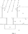
窒化シリコン又はシリコンカーバイドのような中間エッチ停止層14がその上に形成される。低誘電率(k)材料を含有する誘電体層、例えばF−TEOS由来のフッ素ドープシリコン酸化物層のような、他の誘電体層15がその上にデポジションされる。その後、二重ダマシン開口部(16)が形成され、誘電体層13,15の露出表面17が残される。二重ダマシン開口部は、ビア形成後にトレンチ形成(via first-trench last)する技術、又はトレンチ形成後にビア形成(trench first-trench last)する技術の何れによっても形成されることが理解される。誘電体層13,15の露出した表面は、矢印18で示すようにパルス状レーザ光線を照射することによって、レーザ熱アニール処理に晒され、その結果、フッ素が減少し、窒素が濃縮される。
本発明の実施形態の使用に適した他の適切な低誘電率材料は、FOx(登録商標)(HSQベース)、XLK(登録商標)(HSQベース)、多孔質体SILK(登録商標)、芳香族炭化水素ポリマー(それぞれの材料はミシガン州ミッドランド市のダウ化学株式会社から入手可能:Dow Chemical Co.,Midland, MI):Coral(登録商標)、炭素ドープシリコン酸化物(カリフォルニア州サンノゼ市のノベラスシステム会社から入手可能:Novellus Systems, San Jose, CA)、シリコン−炭素−酸素−炭化水素(SiCOH)有機誘電体、Black-Diamond(登録商標)誘電体、Flare(登録商標)、有機ポリマー、HOSP(登録商標)、ハイブリッドシオロキサン有機ポリマー(hybrid sioloxane-organic polymer)、Nanoglassナノグラス(登録商標)、ナノ多孔質シリカ(個々の材料は、ハネウェル電気材料会社から入手可能)、オルトけい酸テトラエチル(TEOS)由来のハロゲンドープ(例えばフッ素ドープ)シリコン酸化物、フッ素ドープシリケートグラス(fluorine-doped silicate glass:FSG)を有する。
Claims (13)
- 誘電体層に開口部を形成する過程と、
アンモニア(NH3)及び窒素(N2)中で前記誘電体層の露出表面領域にレーザ熱アニール処理を実行し、
タンタル(Ta)を含有し前記開口部を被覆する複合バリア層を形成する過程と、を含む、半導体デバイスの製造方法。 - 前記誘電体層が、フッ素ドープオルトけい酸テトラエチル(F−TEOS)由来のフッ素含有シリコン酸化物を含む、請求項1記載の方法。
- フッ素(F)が減少して窒素(N2)が濃縮された表面領域を形成するため、前記露出表面にレーザ熱アニール処理を実行する過程を含む、請求項2記載の方法。
- 誘電体層に開口部を形成する過程と、
フッ素(F)が減少して窒素(N2)が濃縮された表面領域を形成するため、アンモニア(NH3)及び窒素(N2)中で前記誘電体層の露出表面領域にレーザ熱アニール処理を実行し、
タンタル(Ta)のデポジションを行うことによって、タンタル(Ta)を含有し前記開口部を被覆する複合バリア層を形成する過程とを含み、
前記誘電体層が、フッ素ドープオルトけい酸テトラエチル(F−TEOS)由来のフッ素含有シリコン酸化物を含み、
前記複合バリア層は、前記窒素(N2)が濃縮された表面領域上に形成されるとともに前記窒素が濃縮された表面領域から離れる方向で窒素(N2)量が減少するように窒素を含有する傾斜濃度窒化タンタル層と、前記傾斜濃度窒化タンタル層(20)に形成されたαタンタル(α−Ta)層(21)とを含む、半導体デバイスの製造方法。 - 前記開口部を銅(Cu)又は銅合金で充填する過程を含む、請求項4記載の方法。
- 前記開口部は、上方トレンチにつながる下方ビアホールを含むデュアルダマシン開口部を含み、
上方ラインとつながった下方ビアを形成するように前記前記開口部を銅(Cu)又は銅合金で充填する過程を含む、請求項5記載の方法。 - 0.09〜0.11ジュール/cm 2 の放射フルーエンスで前記露出表面にレーザ光線(18)を照射することによってレーザ熱アニール処理する過程を含む、請求項6記載の方法。
- 温度を370℃〜430℃に上昇させるように前記レーザ熱アニール処理を行う過程を含む、請求項7記載の方法。
- 窒素(N2)を流速200〜2000sccm、アンモニア(NH3)を流速200〜2000sccmで用いたレーザ熱アニール処理を行って、フッ素(F)が減少されて窒素(N2)が濃縮された表面領域を形成する過程を含む、請求項2記載の方法。
- タンタル(Ta)のデポジションを行うことによって前記複合バリア層(20,21)を形成する過程を有し、前記複合バリア層は、
前記窒素が濃縮された表面領域上に形成された傾斜濃度窒化タンタル層を有し、この傾斜濃度窒化タンタル層は、前記窒素濃縮表面領域(19)から離れる方向で窒素(N2)量が減少するように窒素を含有するものであり、
前記傾斜濃度窒化タンタル層上に形成されたαタンタル(α−Ta)層(21)を有する、請求項9記載の方法。 - 窒素(N2)が濃縮された表面領域を形成するように前記誘電層の露出表面にレーザ熱アニール処理を実行する過程を含む、請求項1記載の方法。
- タンタル(Ta)のデポジションを行うことによって前記複合バリア層(20,21)を形成する過程を有し、前記複合バリア層は、
前記窒素が濃縮された表面領域上に形成された傾斜濃度窒化タンタル層を有し、この傾斜濃度窒化タンタル層は、前記窒素濃縮表面領域(19)から離れる方向で窒素(N2)量が減少するように窒素を含有するものであり、
前記傾斜濃度窒化タンタル層上に形成されたαタンタル(α−Ta)層(21)を有する、請求項11記載の方法。 - 前記開口部を銅(Cu)又は銅合金で充填する過程を含む、請求項11記載の方法。
Applications Claiming Priority (3)
| Application Number | Priority Date | Filing Date | Title |
|---|---|---|---|
| US10/001,805 | 2001-12-05 | ||
| US10/001,805 US6645853B1 (en) | 2001-12-05 | 2001-12-05 | Interconnects with improved barrier layer adhesion |
| PCT/US2002/038820 WO2003049161A1 (en) | 2001-12-05 | 2002-12-04 | Interconnects with improved barrier layer adhesion |
Publications (3)
| Publication Number | Publication Date |
|---|---|
| JP2005512322A JP2005512322A (ja) | 2005-04-28 |
| JP2005512322A5 JP2005512322A5 (ja) | 2006-01-26 |
| JP4740538B2 true JP4740538B2 (ja) | 2011-08-03 |
Family
ID=21697916
Family Applications (1)
| Application Number | Title | Priority Date | Filing Date |
|---|---|---|---|
| JP2003550266A Expired - Lifetime JP4740538B2 (ja) | 2001-12-05 | 2002-12-04 | 半導体デバイスの製造方法 |
Country Status (8)
| Country | Link |
|---|---|
| US (2) | US6645853B1 (ja) |
| EP (1) | EP1451858B1 (ja) |
| JP (1) | JP4740538B2 (ja) |
| KR (2) | KR101059968B1 (ja) |
| CN (1) | CN1316566C (ja) |
| AU (1) | AU2002362062A1 (ja) |
| TW (1) | TWI265593B (ja) |
| WO (1) | WO2003049161A1 (ja) |
Families Citing this family (32)
| Publication number | Priority date | Publication date | Assignee | Title |
|---|---|---|---|---|
| TW518712B (en) * | 2002-01-25 | 2003-01-21 | Taiwan Semiconductor Mfg | Manufacture method of low resistance barrier layer of copper metallization process |
| US6664185B1 (en) * | 2002-04-25 | 2003-12-16 | Advanced Micro Devices, Inc. | Self-aligned barrier formed with an alloy having at least two dopant elements for minimized resistance of interconnect |
| US7060557B1 (en) * | 2002-07-05 | 2006-06-13 | Newport Fab, Llc, Inc. | Fabrication of high-density capacitors for mixed signal/RF circuits |
| US6780789B1 (en) * | 2002-08-29 | 2004-08-24 | Advanced Micro Devices, Inc. | Laser thermal oxidation to form ultra-thin gate oxide |
| US7825516B2 (en) * | 2002-12-11 | 2010-11-02 | International Business Machines Corporation | Formation of aligned capped metal lines and interconnections in multilevel semiconductor structures |
| US20050104072A1 (en) | 2003-08-14 | 2005-05-19 | Slater David B.Jr. | Localized annealing of metal-silicon carbide ohmic contacts and devices so formed |
| US6992390B2 (en) * | 2003-11-07 | 2006-01-31 | International Business Machines Corp. | Liner with improved electromigration redundancy for damascene interconnects |
| KR100515370B1 (ko) * | 2003-12-31 | 2005-09-14 | 동부아남반도체 주식회사 | 반도체 소자의 플러그 제조 방법 |
| US6952052B1 (en) * | 2004-03-30 | 2005-10-04 | Advanced Micro Devices, Inc. | Cu interconnects with composite barrier layers for wafer-to-wafer uniformity |
| US7605469B2 (en) * | 2004-06-30 | 2009-10-20 | Intel Corporation | Atomic layer deposited tantalum containing adhesion layer |
| US7223670B2 (en) | 2004-08-20 | 2007-05-29 | International Business Machines Corporation | DUV laser annealing and stabilization of SiCOH films |
| US7087521B2 (en) * | 2004-11-19 | 2006-08-08 | Intel Corporation | Forming an intermediate layer in interconnect joints and structures formed thereby |
| US20060113675A1 (en) * | 2004-12-01 | 2006-06-01 | Chung-Liang Chang | Barrier material and process for Cu interconnect |
| US7528028B2 (en) * | 2005-06-17 | 2009-05-05 | Taiwan Semiconductor Manufacturing Company, Ltd. | Super anneal for process induced strain modulation |
| KR100640662B1 (ko) * | 2005-08-06 | 2006-11-01 | 삼성전자주식회사 | 장벽금속 스페이서를 구비하는 반도체 소자 및 그 제조방법 |
| KR100687436B1 (ko) * | 2005-12-26 | 2007-02-26 | 동부일렉트로닉스 주식회사 | 반도체소자의 구리배선막 형성방법 |
| US20070235876A1 (en) * | 2006-03-30 | 2007-10-11 | Michael Goldstein | Method of forming an atomic layer thin film out of the liquid phase |
| US7800228B2 (en) * | 2006-05-17 | 2010-09-21 | International Business Machines Corporation | Reliable via contact interconnect structure |
| KR100853098B1 (ko) * | 2006-12-27 | 2008-08-19 | 동부일렉트로닉스 주식회사 | 반도체 소자의 금속 배선 및 이의 제조 방법 |
| US7851343B2 (en) * | 2007-06-14 | 2010-12-14 | Cree, Inc. | Methods of forming ohmic layers through ablation capping layers |
| US20090102052A1 (en) * | 2007-10-22 | 2009-04-23 | Sang Wook Ryu | Semiconductor Device and Fabricating Method Thereof |
| US20090179328A1 (en) * | 2008-01-14 | 2009-07-16 | International Business Machines Corporation | Barrier sequence for use in copper interconnect metallization |
| CN101494191B (zh) * | 2008-01-24 | 2011-03-23 | 中芯国际集成电路制造(上海)有限公司 | 一种双镶嵌结构的制造方法 |
| US8105937B2 (en) * | 2008-08-13 | 2012-01-31 | International Business Machines Corporation | Conformal adhesion promoter liner for metal interconnects |
| US20100099251A1 (en) * | 2008-10-22 | 2010-04-22 | Applied Materials, Inc. | Method for nitridation pretreatment |
| KR101277272B1 (ko) | 2008-12-08 | 2013-06-20 | 한국전자통신연구원 | 조류인플루엔자 바이러스의 포획 및 억제용 펩타이드 화합물 및 그의 응용 |
| CN102420176A (zh) * | 2011-06-15 | 2012-04-18 | 上海华力微电子有限公司 | 一种改善半导体晶片翘曲的方法 |
| US8420531B2 (en) * | 2011-06-21 | 2013-04-16 | International Business Machines Corporation | Enhanced diffusion barrier for interconnect structures |
| JP5835696B2 (ja) | 2012-09-05 | 2015-12-24 | 株式会社東芝 | 半導体装置およびその製造方法 |
| US11443983B2 (en) * | 2018-09-24 | 2022-09-13 | Intel Corporation | Void-free high aspect ratio metal alloy interconnects and method of manufacture using a solvent-based etchant |
| CN110970350A (zh) * | 2018-09-28 | 2020-04-07 | 长鑫存储技术有限公司 | 包含α-Ta层的扩散阻挡层的制备方法以及复合扩散阻挡层 |
| CN110112096A (zh) * | 2019-05-17 | 2019-08-09 | 长江存储科技有限责任公司 | 金属互连结构及其形成方法 |
Citations (5)
| Publication number | Priority date | Publication date | Assignee | Title |
|---|---|---|---|---|
| JPH0258216A (ja) * | 1988-08-23 | 1990-02-27 | Sony Corp | 半導体集積回路装置の製造方法 |
| JPH09162291A (ja) * | 1995-12-06 | 1997-06-20 | Ricoh Co Ltd | 半導体装置の製造方法 |
| JP2000323476A (ja) * | 1999-05-12 | 2000-11-24 | Tokyo Electron Ltd | 配線構造およびその製造方法 |
| JP2001053077A (ja) * | 1999-08-13 | 2001-02-23 | Hitachi Ltd | 半導体集積回路装置およびその製造方法 |
| JP2001230256A (ja) * | 2000-01-31 | 2001-08-24 | Motorola Inc | 半導体素子接着層構造および構造形成プロセス |
Family Cites Families (20)
| Publication number | Priority date | Publication date | Assignee | Title |
|---|---|---|---|---|
| US5464792A (en) * | 1993-06-07 | 1995-11-07 | Motorola, Inc. | Process to incorporate nitrogen at an interface of a dielectric layer in a semiconductor device |
| US6271120B1 (en) | 1995-03-10 | 2001-08-07 | Advanced Micro Devices, Inc. | Method of enhanced silicide layer for advanced metal diffusion barrier layer application |
| US5801097A (en) * | 1997-03-10 | 1998-09-01 | Vanguard International Semiconductor Corporation | Thermal annealing method employing activated nitrogen for forming nitride layers |
| US6448655B1 (en) * | 1998-04-28 | 2002-09-10 | International Business Machines Corporation | Stabilization of fluorine-containing low-k dielectrics in a metal/insulator wiring structure by ultraviolet irradiation |
| US6461675B2 (en) * | 1998-07-10 | 2002-10-08 | Cvc Products, Inc. | Method for forming a copper film on a substrate |
| US6265779B1 (en) * | 1998-08-11 | 2001-07-24 | International Business Machines Corporation | Method and material for integration of fuorine-containing low-k dielectrics |
| US6146996A (en) | 1998-09-01 | 2000-11-14 | Philips Electronics North America Corp. | Semiconductor device with conductive via and method of making same |
| TW520551B (en) * | 1998-09-24 | 2003-02-11 | Applied Materials Inc | Method for fabricating ultra-low resistivity tantalum films |
| US6143650A (en) | 1999-01-13 | 2000-11-07 | Advanced Micro Devices, Inc. | Semiconductor interconnect interface processing by pulse laser anneal |
| US6156648A (en) * | 1999-03-10 | 2000-12-05 | United Microelectronics Corp. | Method for fabricating dual damascene |
| US6222579B1 (en) * | 1999-05-14 | 2001-04-24 | Presstek, Inc. | Alignment of laser imaging assembly |
| US6339258B1 (en) * | 1999-07-02 | 2002-01-15 | International Business Machines Corporation | Low resistivity tantalum |
| US6326301B1 (en) * | 1999-07-13 | 2001-12-04 | Motorola, Inc. | Method for forming a dual inlaid copper interconnect structure |
| US6355153B1 (en) * | 1999-09-17 | 2002-03-12 | Nutool, Inc. | Chip interconnect and packaging deposition methods and structures |
| US6319766B1 (en) | 2000-02-22 | 2001-11-20 | Applied Materials, Inc. | Method of tantalum nitride deposition by tantalum oxide densification |
| US6284657B1 (en) * | 2000-02-25 | 2001-09-04 | Chartered Semiconductor Manufacturing Ltd. | Non-metallic barrier formation for copper damascene type interconnects |
| US6657284B1 (en) * | 2000-12-01 | 2003-12-02 | Taiwan Semiconductor Manufacturing Co., Ltd. | Graded dielectric layer and method for fabrication thereof |
| US6429524B1 (en) * | 2001-05-11 | 2002-08-06 | International Business Machines Corporation | Ultra-thin tantalum nitride copper interconnect barrier |
| US6548400B2 (en) * | 2001-06-29 | 2003-04-15 | Texas Instruments Incorporated | Method of fabricating interlevel connectors using only one photomask step |
| US6930391B2 (en) * | 2002-08-27 | 2005-08-16 | Intel Corporation | Method for alloy-electroplating group IB metals with refractory metals for interconnections |
-
2001
- 2001-12-05 US US10/001,805 patent/US6645853B1/en not_active Expired - Lifetime
-
2002
- 2002-12-04 KR KR1020097017642A patent/KR101059968B1/ko active IP Right Grant
- 2002-12-04 KR KR1020047008728A patent/KR100922420B1/ko active IP Right Grant
- 2002-12-04 CN CNB028242548A patent/CN1316566C/zh not_active Expired - Lifetime
- 2002-12-04 AU AU2002362062A patent/AU2002362062A1/en not_active Abandoned
- 2002-12-04 JP JP2003550266A patent/JP4740538B2/ja not_active Expired - Lifetime
- 2002-12-04 EP EP02797192A patent/EP1451858B1/en not_active Expired - Lifetime
- 2002-12-04 WO PCT/US2002/038820 patent/WO2003049161A1/en active Application Filing
- 2002-12-05 TW TW091135258A patent/TWI265593B/zh not_active IP Right Cessation
-
2003
- 2003-09-16 US US10/662,525 patent/US7071562B2/en not_active Expired - Lifetime
Patent Citations (5)
| Publication number | Priority date | Publication date | Assignee | Title |
|---|---|---|---|---|
| JPH0258216A (ja) * | 1988-08-23 | 1990-02-27 | Sony Corp | 半導体集積回路装置の製造方法 |
| JPH09162291A (ja) * | 1995-12-06 | 1997-06-20 | Ricoh Co Ltd | 半導体装置の製造方法 |
| JP2000323476A (ja) * | 1999-05-12 | 2000-11-24 | Tokyo Electron Ltd | 配線構造およびその製造方法 |
| JP2001053077A (ja) * | 1999-08-13 | 2001-02-23 | Hitachi Ltd | 半導体集積回路装置およびその製造方法 |
| JP2001230256A (ja) * | 2000-01-31 | 2001-08-24 | Motorola Inc | 半導体素子接着層構造および構造形成プロセス |
Also Published As
| Publication number | Publication date |
|---|---|
| AU2002362062A1 (en) | 2003-06-17 |
| KR20090095680A (ko) | 2009-09-09 |
| US6645853B1 (en) | 2003-11-11 |
| TW200304202A (en) | 2003-09-16 |
| CN1599949A (zh) | 2005-03-23 |
| WO2003049161A1 (en) | 2003-06-12 |
| EP1451858A1 (en) | 2004-09-01 |
| CN1316566C (zh) | 2007-05-16 |
| EP1451858B1 (en) | 2012-02-22 |
| KR20050044734A (ko) | 2005-05-12 |
| US7071562B2 (en) | 2006-07-04 |
| JP2005512322A (ja) | 2005-04-28 |
| KR100922420B1 (ko) | 2009-10-16 |
| KR101059968B1 (ko) | 2011-08-29 |
| US20040063310A1 (en) | 2004-04-01 |
| TWI265593B (en) | 2006-11-01 |
Similar Documents
| Publication | Publication Date | Title |
|---|---|---|
| JP4740538B2 (ja) | 半導体デバイスの製造方法 | |
| KR100892403B1 (ko) | 신뢰성 있는 구리 상호연결구조 형성 방법 | |
| US6509267B1 (en) | Method of forming low resistance barrier on low k interconnect with electrolessly plated copper seed layer | |
| JP4956919B2 (ja) | 半導体装置およびその製造方法 | |
| US6429128B1 (en) | Method of forming nitride capped Cu lines with reduced electromigration along the Cu/nitride interface | |
| US6764951B1 (en) | Method for forming nitride capped Cu lines with reduced hillock formation | |
| TW526590B (en) | Integration of organic fill for dual damascene process | |
| US6555461B1 (en) | Method of forming low resistance barrier on low k interconnect | |
| US6664187B1 (en) | Laser thermal annealing for Cu seedlayer enhancement | |
| US6989601B1 (en) | Copper damascene with low-k capping layer and improved electromigration reliability | |
| US6723634B1 (en) | Method of forming interconnects with improved barrier layer adhesion | |
| US6731006B1 (en) | Doped copper interconnects using laser thermal annealing | |
| US6743310B1 (en) | Method of forming nitride capped Cu lines with improved adhesion and reduced electromigration along the Cu/nitride interface | |
| US6713874B1 (en) | Semiconductor devices with dual nature capping/arc layers on organic-doped silica glass inter-layer dielectrics | |
| US6576545B1 (en) | Semiconductor devices with dual nature capping/ARC layers on fluorine doped silica glass inter-layer dielectrics and method of forming capping/ARC layers | |
| KR100852207B1 (ko) | 절연막 제거방법 및 금속 배선 형성방법 | |
| JPH1116906A (ja) | 半導体装置及びその製造方法 | |
| US6897144B1 (en) | Cu capping layer deposition with improved integrated circuit reliability | |
| KR20100073779A (ko) | 반도체 소자의 금속배선 및 그 제조 방법 | |
| KR20020091307A (ko) | 반도체 소자의 금속 배선 형성방법 |
Legal Events
| Date | Code | Title | Description |
|---|---|---|---|
| A521 | Request for written amendment filed |
Free format text: JAPANESE INTERMEDIATE CODE: A523 Effective date: 20051205 |
|
| A621 | Written request for application examination |
Free format text: JAPANESE INTERMEDIATE CODE: A621 Effective date: 20051205 |
|
| A977 | Report on retrieval |
Free format text: JAPANESE INTERMEDIATE CODE: A971007 Effective date: 20070927 |
|
| A131 | Notification of reasons for refusal |
Free format text: JAPANESE INTERMEDIATE CODE: A131 Effective date: 20090512 |
|
| A521 | Request for written amendment filed |
Free format text: JAPANESE INTERMEDIATE CODE: A523 Effective date: 20090810 |
|
| RD03 | Notification of appointment of power of attorney |
Free format text: JAPANESE INTERMEDIATE CODE: A7423 Effective date: 20100421 |
|
| RD05 | Notification of revocation of power of attorney |
Free format text: JAPANESE INTERMEDIATE CODE: A7425 Effective date: 20100902 |
|
| A02 | Decision of refusal |
Free format text: JAPANESE INTERMEDIATE CODE: A02 Effective date: 20100908 |
|
| A521 | Request for written amendment filed |
Free format text: JAPANESE INTERMEDIATE CODE: A523 Effective date: 20110106 |
|
| A911 | Transfer to examiner for re-examination before appeal (zenchi) |
Free format text: JAPANESE INTERMEDIATE CODE: A911 Effective date: 20110223 |
|
| TRDD | Decision of grant or rejection written | ||
| A01 | Written decision to grant a patent or to grant a registration (utility model) |
Free format text: JAPANESE INTERMEDIATE CODE: A01 Effective date: 20110330 |
|
| A61 | First payment of annual fees (during grant procedure) |
Free format text: JAPANESE INTERMEDIATE CODE: A61 Effective date: 20110502 |
|
| R150 | Certificate of patent or registration of utility model |
Ref document number: 4740538 Country of ref document: JP Free format text: JAPANESE INTERMEDIATE CODE: R150 Free format text: JAPANESE INTERMEDIATE CODE: R150 |
|
| FPAY | Renewal fee payment (event date is renewal date of database) |
Free format text: PAYMENT UNTIL: 20140513 Year of fee payment: 3 |
|
| R250 | Receipt of annual fees |
Free format text: JAPANESE INTERMEDIATE CODE: R250 |
|
| R250 | Receipt of annual fees |
Free format text: JAPANESE INTERMEDIATE CODE: R250 |
|
| R250 | Receipt of annual fees |
Free format text: JAPANESE INTERMEDIATE CODE: R250 |
|
| R250 | Receipt of annual fees |
Free format text: JAPANESE INTERMEDIATE CODE: R250 |
|
| R250 | Receipt of annual fees |
Free format text: JAPANESE INTERMEDIATE CODE: R250 |
|
| R250 | Receipt of annual fees |
Free format text: JAPANESE INTERMEDIATE CODE: R250 |
|
| R250 | Receipt of annual fees |
Free format text: JAPANESE INTERMEDIATE CODE: R250 |
|
| R250 | Receipt of annual fees |
Free format text: JAPANESE INTERMEDIATE CODE: R250 |
|
| R250 | Receipt of annual fees |
Free format text: JAPANESE INTERMEDIATE CODE: R250 |
|
| EXPY | Cancellation because of completion of term |