JP4727018B2 - Active matrix display device - Google Patents
Active matrix display device Download PDFInfo
- Publication number
- JP4727018B2 JP4727018B2 JP2000053470A JP2000053470A JP4727018B2 JP 4727018 B2 JP4727018 B2 JP 4727018B2 JP 2000053470 A JP2000053470 A JP 2000053470A JP 2000053470 A JP2000053470 A JP 2000053470A JP 4727018 B2 JP4727018 B2 JP 4727018B2
- Authority
- JP
- Japan
- Prior art keywords
- shielding film
- film
- pixel
- light
- source signal
- Prior art date
- Legal status (The legal status is an assumption and is not a legal conclusion. Google has not performed a legal analysis and makes no representation as to the accuracy of the status listed.)
- Expired - Lifetime
Links
Images


Landscapes
- Liquid Crystal (AREA)
- Devices For Indicating Variable Information By Combining Individual Elements (AREA)
- Thin Film Transistor (AREA)
Description
【0001】
【発明の属する技術分野】
本願発明は絶縁表面を有する基板上に薄膜トランジスタ(以下、TFTという)で構成された回路を有する半導体装置およびその作製方法に関する。特に本願発明は、画素マトリクス回路とその周辺に設けられる駆動回路を同一基板上に設けた液晶表示装置に代表される電気光学装置、および電気光学装置を搭載した電子機器に関する。尚、本願明細書において半導体装置とは、半導体特性を利用することで機能する装置全般を指し、上記電気光学装置およびその電気光学装置を搭載した電子機器も半導体装置に含む。
【0002】
【従来の技術】
最近、安価なガラス基板上に薄膜トランジスタ(TFT)を作製する技術が急速に発達してきている。その理由は、アクティブマトリクス型液晶表示装置の需要が高まったことにある。アクティブマトリクス型液晶表示装置は、マトリクス状に配置された数十〜数百万個もの各画素のそれぞれに薄膜トランジスタを配置し、各画素電極に出入りする電荷を薄膜トランジスタのスイッチング機能により制御するものである。
【0003】
各画素電極と対向電極との間には液晶が挟み込まれ、一種のコンデンサを形成している。従って、薄膜トランジスタによりこのコンデンサへの電荷の出入りを制御することで液晶の電気光学的特性を変化させ、液晶パネルを透過する光を制御して画像表示を行うことができる。また、このような構成でなるコンデンサは電流のリークにより次第にその保持電圧が減少するため、液晶の電気光学特性が変化して画像表示のコントラストが悪化するという問題を持つ。
【0004】
そこで、液晶で構成されるコンデンサと直列に保持容量と呼ばれる別のコンデンサを設置し、リーク等で損失した電荷を液晶で構成されるコンデンサに供給する構成が一般的となっている。
【0005】
保持容量の構造は様々であるが、遮蔽膜と画素電極との間に誘電体としての酸化膜を挟み込んだ構造が挙げられる。遮蔽膜とは、透過型液晶表示装置の画素マトリクス部において、薄膜トランジスタが光の照射によって導電性が変動するのを防止するための、遮光性を有する被膜である。
【発明が解決しようとする課題】
遮蔽膜と画素電極との間に誘電体を挟み込んだ構造の保持容量は、遮蔽膜を一定の電位に保つために、基準電位が印加されたコモン線に接続されている。
【0006】
そこで工程上、遮蔽膜をパターニングによって形成した後に、遮蔽膜とコモン線を接続するために、遮蔽膜とコモン線との間に設けられた層間絶縁膜にコンタクトホールをあける必要があった。コンタクトホールはマスクを用いたフォトリソグラフィーによって形成される。
【0007】
アクティブマトリクス型液晶表示装置は、その作製工程においてマスクを用いたフォトリソグラフィーを、遮蔽膜とコモン線の間に設けられた層間絶縁膜にコンタクトホールをあける工程の他に、例えば活性層の形成工程、ゲート絶縁膜の形成工程、画素電極の形成工程、ゲート線及びソース信号線の形成工程等で行っている。マスクを用いたフォトリソグラフィーは、アクティブマトリクス型液晶表示装置の作製工程数を増やす要因となっており、高い歩留まりを達成するためには、作製工程数を減らすことが望まれていた。
【0008】
【課題を解決するための手段】
アクティブマトリクス型液晶表示装置において、画素TFTに接続しているソース信号線に逆の極性の電圧を印加する駆動方法をソースライン反転という。このソースライン反転とは、液晶に常に1つの向きの電界が印加されることによって、液晶が劣化するのを防ぐために行われる。図4に示すように、ソース信号線1ラインごとに極性が逆の信号を印加し、1フレーム期間ごとに信号の極性を反転させることで、液晶に常に1つの向きの電界が印加されることによって液晶が劣化するのを防ぐ。1フレーム期間とは全ての画素が1つの画面を表示する期間を示す。
【0009】
このソースライン反転を用いた場合、遮蔽膜の電位の変動も平均化される。そのために、遮蔽膜を一定の電位(基準電位)に保たれたコモン線に接続しなくても、遮蔽膜の電位は時間的に平均を取るとほぼ一定に保たれるので、遮蔽膜と画素電極との間に誘電体を挟み込んだ構造の保持容量において、遮蔽膜をフローティングにすることが可能になる。よって遮蔽膜をパターニングによって形成した後に、遮蔽膜とコモン線とを接続するために、遮蔽膜とコモン線との間に設けられた層間絶縁膜にマスクを用いたフォトリソグラフィーによってコンタクトホールをあける必要がなくなる。よってアクティブマトリクス型液晶表示装の作製工程を削減し、高い歩留まりを達成することが可能になり、またその作製コストを抑えることが可能になる。
【0010】
また上記構成に加えて、遮蔽膜とコモン線との間に大容量のカップリング容量を形成すると、遮蔽膜の電位の変動ΔVが小さくなる。ΔVは遮蔽膜とコモン線との間に形成されるカップリング容量の容量値Cと遮蔽膜にかかる電荷量Qによって、その値が決まる。しかし、電荷量Qは画素数、ソース信号線に入力される信号の電圧の値によって固定されてしまうので、実際には遮蔽膜の電位の変動ΔVの値はカップリング容量の容量値Cによって決定されてしまう。このCの値が大きければ大きいほどΔVは小さくなり、遮蔽膜の電位をより一定に保つことが可能になる。
【0011】
遮蔽膜をフローティングにして遮蔽膜とコモン線との間に大容量のカップリング容量を形成した場合、上述した遮蔽膜をフローティングにするだけの構成と同じく、遮蔽膜とコモン線との間に設けられた層間絶縁膜にマスクを用いたフォトリソグラフィーによってコンタクトホールをあける必要がなくなる。カップリング容量の容量値は、ゲート信号線1ラインに画素TFTを介して接続されている全ての保持容量の容量値の合計の10倍以上であれば良い。よってアクティブマトリクス型液晶表示装置の作製工程を削減し、高い歩留まりを達成することが可能になり、またその作製コストを抑えることが可能になる。またそれに加えて、遮蔽膜をフローティングにして遮蔽膜とコモン線との間に大容量のカップリング容量を形成した場合は、遮蔽膜の電位をさらに一定に保つことが可能になるため、良好なコントラストを得ることができる。
【0012】
以下に本願発明の構成を述べる。
【0013】
本願発明のある実施の形態によると、複数の画素TFTと、前記画素TFTに電気的に接続された画素電極と、遮蔽膜とが設けられた基板を有するアクティブマトリクス型液晶表示装置であって、
前記遮蔽膜はフローティングになっており、
前記画素電極と前記遮蔽膜との間に誘電体を有することを特徴とするアクティブマトリクス型液晶表示装置が提供される。このことによって上記目的が達成される。
【0014】
また本願発明のある実施の形態によると、複数のソース信号線と、複数のゲート信号線と、複数の画素TFTと、前記画素TFTに電気的に接続された画素電極と、遮蔽膜とが設けられた基板を有するアクティブマトリクス型液晶表示装置であって、
前記複数の画素TFTは前記ソース信号線と前記ゲート信号線に電気的に接続されており、
前記遮蔽膜はフローティングになっており、
前記画素電極と前記遮蔽膜との間に誘電体が設けられており、
前記複数のソース信号線1本ごとに極性が逆の信号を印加し、前記複数のソース信号線のそれぞれに印加される前記信号の極性を1フレーム期間ごとに反転させることを特徴とするアクティブマトリクス型液晶表示装置が提供される。このことによって上記目的が達成される。
【0015】
また本願発明のある実施の形態によると、複数のソース信号線と、複数のゲート信号線と、複数の画素TFTと、画素電極と、遮蔽膜とが設けられた第1の基板と、
対向電極が設けられた第2の基板と、
前記画素電極と前記対向電極との間に挟まれた液晶と、
を有するアクティブマトリクス型液晶表示装置において、
前記各画素TFTは、ゲート電極と、ゲート絶縁膜と、ソース領域、ドレイン領域及びチャネル形成領域を有する活性層とを有し、
前記ゲート電極は前記ゲート信号線に接続されており、
前記ソース領域またはドレイン領域は前記ソース信号線に接続されており、
前記ドレイン領域またはソース領域は前記画素電極に接続されており、
前記画素電極と前記遮蔽膜の間に誘電体が設けられており、
前記遮蔽膜はフローティングになっており、
前記複数のソース信号線1本ごとに極性が逆の信号を印加し、前記複数のソース信号線のそれぞれに印加される前記信号の極性を1フレーム期間ごとに反転させることを特徴とするアクティブマトリクス型液晶表示装置が提供される。このことによって上記目的が達成される。
【0016】
また本願発明のある実施の形態によると、複数のソース信号線と、複数のゲート信号線と、複数の画素TFTと、画素電極と、遮蔽膜とが設けられた第1の基板と、
対向電極が設けられた第2の基板と、
前記画素電極と前記対向電極との間に挟まれた液晶と、
を有するアクティブマトリクス型液晶表示装置において、
前記各画素TFTは、ゲート電極と、ゲート絶縁膜と、活性層とを有し、
前記活性層はチャネル形成領域と、前記チャネル形成領域に接している第2の不純物領域と、前記第2の不純物領域に接している第1の不純物領域を有し、
前記ゲート電極は前記ゲート信号線に接続されており、
前記第1の不純物領域の一方は前記画素電極に接続されており、
前記第1の不純物領域のもう一方は前記ソース信号線に接続されており、
前記画素電極と前記遮蔽膜の間に誘電体が設けられており、
前記遮蔽膜はフローティングになっており、
前記第2の不純物領域は、前記ゲート絶縁膜を介して、前記ゲート電極と重なっており、
前記複数のソース信号線1本ごとに極性が逆の信号を印加し、前記複数のソース信号線のそれぞれに印加される前記信号の極性を1フレーム期間ごとに反転させることを特徴とするアクティブマトリクス型液晶表示装置が提供される。このことによって上記目的が達成される。
【0017】
また本願発明のある実施の形態によると、複数のソース信号線と、複数のゲート信号線と、複数の画素TFTと、画素電極と、遮蔽膜とが設けられた第1の基板と、
対向電極が設けられた第2の基板と、
前記画素電極と前記対向電極との間に挟まれた液晶と、
を有するアクティブマトリクス型液晶表示装置において、
前記各画素TFTは、ゲート電極と、ゲート絶縁膜と、活性層とを有し、
前記活性層はチャネル形成領域と、前記チャネル形成領域に接している第2の不純物領域と、前記チャネル形成領域を挟んで設けられた第1の不純物領域とを有し、
前記ゲート電極は前記ゲート信号線に接続されており、
前記第1の不純物領域の一方は前記画素電極に接続されており、
前記第1の不純物領域のもう一方は前記ソース信号線に接続されており、
前記画素電極と前記遮蔽膜の間に誘電体が設けられており、
前記遮蔽膜はフローティングになっており、
前記第2の不純物領域は、前記ゲート絶縁膜を介して、前記ゲート電極と重なっており、
前記複数のソース信号線1本ごとに極性が逆の信号を印加し、前記複数のソース信号線のそれぞれに印加される前記信号の極性を1フレーム期間ごとに反転させることを特徴とするアクティブマトリクス型液晶表示装置が提供される。このことによって上記目的が達成される。
【0018】
前記誘電体は、前記遮蔽膜を陽極酸化して形成される陽極酸化膜であっても良い。
【0019】
前記遮蔽膜は、アルミニウム(Al)、チタン(Ti)またはタンタル(Ta)を有する膜であっても良い。
【0020】
前記遮蔽膜は100〜300nmの厚さであっても良い。
【0021】
前記ゲート電極は、チタン(Ti)、タンタル(Ta)、タングステン(W)、モリブデン(Mo)、から選ばれた一種または複数種の元素を有していても良い。
【0022】
前記アクティブマトリクス型液晶表示装置を3つ備えたリアプロジェクターであっても良い。
【0023】
前記アクティブマトリクス型液晶表示装置を3つ備えたフロントプロジェクターであっても良い。
【0024】
前記アクティブマトリクス型液晶表示装置を1つ備えた単板式リアプロジェクターであっても良い。
【0025】
前記アクティブマトリクス型液晶表示装置を2備えたゴーグル型ディスプレイであっても良い。
【0026】
また本願発明のある実施の形態によると、複数の画素TFT及び前記複数の画素TFTに電気的に接続された画素電極を有する画素マトリクス部と、遮蔽膜と、一定の基準電位に保たれたコモン線とが設けられた基板を有するアクティブマトリクス型液晶表示装置であって、
前記遮蔽膜はフローティングになっており、
前記画素電極と前記遮蔽膜との間に第1の誘電体を有し、
前記遮蔽膜と前記コモン線との間に第2の誘電体を有し、
前記第2の誘電体は前記画素マトリクス部と重ならないことを特徴とするアクティブマトリクス型液晶表示装置が提供される。このことによって上記目的が達成される。
【0027】
また本願発明のある実施の形態によると、複数の画素TFT及び前記複数の画素TFTに電気的に接続された画素電極を有する画素マトリクス部と、複数のソース信号線と、複数のゲート信号線と、遮蔽膜と、一定の基準電位に保たれたコモン線とが設けられた基板を有するアクティブマトリクス型液晶表示装置であって、
前記複数の画素TFTは前記ソース信号線と前記ゲート信号線に電気的に接続されており、
前記遮蔽膜はフローティングになっており、
前記画素電極と前記遮蔽膜との間に第1の誘電体を有し、
前記遮蔽膜と前記コモン線との間に第2の誘電体を有し、
前記第2の誘電体は前記画素マトリクス部と重なっておらず、
前記複数のソース信号線1本ごとに極性が逆の信号を印加し、前記複数のソース信号線のそれぞれに印加される前記信号の極性を1フレーム期間ごとに反転させることを特徴とするアクティブマトリクス型液晶表示装置が提供される。このことによって上記目的が達成される。
【0028】
また本願発明のある実施の形態によると、複数の画素TFT及び前記複数の画素TFTに電気的に接続された画素電極を有する画素マトリクス部と、複数のソース信号線と、複数のゲート信号線と、遮蔽膜と、一定の基準電位に保たれたコモン線とが設けられた第1の基板と、
対向電極が設けられた第2の基板と、
前記画素電極と前記対向電極との間に挟まれた液晶と、
を有するアクティブマトリクス型液晶表示装置において、
前記各画素TFTは、ゲート電極と、ゲート絶縁膜と、ソース領域、ドレイン領域及びチャネル形成領域を有する活性層とを有し、
前記ゲート電極は前記ゲート信号線に接続されており、
前記ソース領域またはドレイン領域は前記ソース信号線に接続されており、
前記ドレイン領域またはソース領域は前記画素電極に接続されており、
前記遮蔽膜はフローティングになっており、
前記画素電極と前記遮蔽膜との間に第1の誘電体を有し、
前記遮蔽膜と前記コモン線との間に第2の誘電体を有し、
前記第2の誘電体は前記画素マトリクス部と重なっておらず、
前記複数のソース信号線1本ごとに極性が逆の信号を印加し、前記複数のソース信号線のそれぞれに印加される前記信号の極性を1フレーム期間ごとに反転させることを特徴とするアクティブマトリクス型液晶表示装置が提供される。このことによって上記目的が達成される。
【0029】
また本願発明のある実施の形態によると、複数の画素TFT及び前記複数の画素TFTに電気的に接続された画素電極を有する画素マトリクス部と、複数のソース信号線と、複数のゲート信号線と、遮蔽膜と、一定の基準電位に保たれたコモン線とが設けられた第1の基板と、
対向電極が設けられた第2の基板と、
前記画素電極と前記対向電極との間に挟まれた液晶と、
を有するアクティブマトリクス型液晶表示装置において、
前記各画素TFTは、ゲート電極と、ゲート絶縁膜と、活性層とを有し、
前記活性層はチャネル形成領域と、前記チャネル形成領域に接している第2の不純物領域と、前記第2の不純物領域に接している第1の不純物領域を有し、
前記ゲート電極は前記ゲート信号線に接続されており、
前記第1の不純物領域の一方は前記画素電極に接続されており、
前記第1の不純物領域のもう一方は前記ソース信号線に接続されており、
前記遮蔽膜はフローティングになっており、
前記画素電極と前記遮蔽膜との間に第1の誘電体を有し、
前記遮蔽膜と前記コモン線との間に第2の誘電体を有し、
前記第2の誘電体は前記画素マトリクス部と重なっておらず、
前記第2の不純物領域は、前記ゲート絶縁膜を介して、前記ゲート電極と重なっており、
前記複数のソース信号線1本ごとに極性が逆の信号を印加し、前記複数のソース信号線のそれぞれに印加される前記信号の極性を1フレーム期間ごとに反転させることを特徴とするアクティブマトリクス型液晶表示装置が提供される。このことによって上記目的が達成される。
【0030】
また本願発明のある実施の形態によると、複数の画素TFT及び前記複数の画素TFTに電気的に接続された画素電極を有する画素マトリクス部と、複数のソース信号線と、複数のゲート信号線と、遮蔽膜と、一定の基準電位に保たれたコモン線とが設けられた第1の基板と、
対向電極が設けられた第2の基板と、
前記画素電極と前記対向電極との間に挟まれた液晶と、
を有するアクティブマトリクス型液晶表示装置において、
前記各画素TFTは、ゲート電極と、ゲート絶縁膜と、活性層とを有し、
前記活性層はチャネル形成領域と、前記チャネル形成領域に接している第2の不純物領域と、前記チャネル形成領域を挟んで設けられた第1の不純物領域とを有し、
前記ゲート電極は前記ゲート信号線に接続されており、
前記第1の不純物領域の一方は前記画素電極に接続されており、
前記第1の不純物領域のもう一方は前記ソース信号線に接続されており、
前記遮蔽膜はフローティングになっており、
前記画素電極と前記遮蔽膜との間に第1の誘電体を有し、
前記遮蔽膜と前記コモン線との間に第2の誘電体を有し、
前記第2の誘電体は前記画素マトリクス部と重なっておらず、
前記第2の不純物領域は、前記ゲート絶縁膜を介して、前記ゲート電極と重なっており、
前記複数のソース信号線1本ごとに極性が逆の信号を印加し、前記複数のソース信号線のそれぞれに印加される前記信号の極性を1フレーム期間ごとに反転させることを特徴とするアクティブマトリクス型液晶表示装置が提供される。このことによって上記目的が達成される。
【0031】
また本願発明のある実施の形態によると、複数の画素TFT及び前記複数の画素TFTに電気的に接続された画素電極を有する画素マトリクス部と、遮蔽膜と、一定の基準電位に保たれたコモン線と、ソース信号線駆動回路とが設けられた第1の基板と、
対向遮蔽膜が設けられた第2の基板と、
を有するアクティブマトリクス型液晶表示装置において、
前記遮蔽膜はフローティングになっており、
前記画素電極と前記遮蔽膜との間に第1の誘電体を有し、
前記遮蔽膜と前記コモン線との間に第2の誘電体を有し、
前記第2の誘電体は前記画素マトリクス部と重なっておらず、
前記ソース信号線駆動回路はサンプリング回路を有しており、
前記対向遮蔽膜は、前記遮蔽膜の一部及び前記サンプリング回路と重なっていることを特徴とするアクティブマトリクス型液晶表示装置が提供される。このことによって上記目的が達成される。
【0032】
前記第1の誘電体は、前記遮蔽膜を陽極酸化して形成される陽極酸化膜であっても良い。
【0033】
前記第2の誘電体は、前記遮蔽膜を陽極酸化して形成される陽極酸化膜であっても良い。
【0034】
前記遮蔽膜は、アルミニウム(Al)、チタン(Ti)またはタンタル(Ta)を有する膜であっても良い。
【0035】
前記遮蔽膜は100〜300nmの厚さであっても良い。
【0036】
前記ゲート電極は、チタン(Ti)、タンタル(Ta)、タングステン(W)、モリブデン(Mo)、から選ばれた一種または複数種の元素を有していても良い。
【0037】
前記アクティブマトリクス型液晶表示装置を3つ備えたリアプロジェクターであっても良い。
【0038】
前記アクティブマトリクス型液晶表示装置を3つ備えたフロントプロジェクターであっても良い。
【0039】
前記アクティブマトリクス型液晶表示装置を1つ備えた単板式リアプロジェクターであっても良い。
【0040】
前記アクティブマトリクス型液晶表示装置を2つ備えたゴーグル型ディスプレイであっても良い。
【0041】
なお、本願発明の遮蔽膜は寄生容量の影響を避けるため、ソース信号線駆動回路上に設けないことが好ましい。
【0042】
【発明の実施の形態】
以下に本願発明を、実施例をもって説明する。ただし、本願発明は、以下の実施例に限定されるわけではない。
【0043】
【実施例】
図1〜図31を用いて、本願発明の実施例を説明する。
【0044】
(実施例1)
本実施例では、本願発明を用いたアクティブマトリクス型液晶表示装置の一例について、図1を用いて説明する。
【0045】
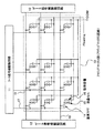
図1に本願発明の保持容量を用いたアクティブマトリクス型液晶表示装置の回路図の一例を示す。ソース信号線駆動回路11、ゲート信号線駆動回路12、アクティブマトリクス回路13、画素TFT14、画素電極と対向電極との間に液晶を挟んだ液晶セル15、画素電極と遮蔽膜の間に誘電体を挟んで形成される保持容量16、ソース信号線17、ゲート信号線18が図1に示されるように設けられている。ソース信号線駆動回路11とゲート信号線駆動回路12は、一般に駆動回路と総称されている。この駆動回路は、アクティブマトリクス回路でなる画素マトリクス部と同一基板上に一体形成されている。
【0046】
また、アクティブマトリクス部13では、ソース信号線駆動回路11に接続されたソース信号線17と、ゲート信号線駆動回路12に接続されたゲート信号線18が交差している。そのソース信号線17とゲート信号線18に囲まれた領域、画素部19に、画素の薄膜トランジスタ(画素TFT)14と、対向電極と画素電極の間に液晶を挟んだ液晶セル15と、保持容量16が設けられている。
【0047】
保持容量16は画素電極と遮蔽膜の間に誘電体としての酸化膜を挟んだ構成となっており、全ての遮蔽膜はコモン線とは接続されていないフローティング(Floating)の状態となっている。
【0048】
ソース信号線17に入力された画像信号は、画素TFT14により選択され、所定の画素電極に書き込まれる。
【0049】
ソース信号線駆動回路11から出力されたタイミング信号によりサンプリングされた画像信号が、ソース信号線17に供給される。
【0050】
画素TFT14は、ゲート信号線駆動回路12からゲート信号線18を介して入力される選択信号により動作する。
【0051】
ソース信号線17に入力される画像信号は、ソース信号線17の1ラインごとに極性を逆にして印加し、1フレーム期間ごとに信号の極性を反転させることで、液晶に常に1つの向きの電界が印加されることによって液晶が劣化するのを防ぐ。このようにソースライン反転で液晶を駆動させて、遮蔽膜をコモン線に接続せずにフローティングとしている。このような構成にすることで、遮蔽膜をコモン線に接続しなくても、遮蔽膜の電位が時間的に平均を取ると一定に保たれるので、遮蔽膜と画素電極との間に誘電体を挟み込んだ構造の保持容量を形成することが可能になる。よって遮蔽膜をパターニングによって形成した後に、遮蔽膜とコモン線を接続するために、遮蔽膜とコモン線との間に設けられた層間絶縁膜にマスクを用いたフォトリソグラフィーによるコンタクトホールをあける必要がなくなる。このため作製工程を削減し、高い歩留まりを達成することが可能になり、またアクティブマトリクス型液晶表示装の作製コストを抑えることが可能になる。
【0052】
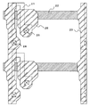
次に、図1における画素部19の詳しい構造について、図2を用いて説明する。
【0053】
まず、図2において、21は活性層、22はゲート信号線、23はソース信号線、24は活性層とソース信号線とのコンタクト部、25はドレイン配線(ドレイン電極)、26は活性層とドレイン配線とのコンタクト部である。
【0054】
次に、図3は、図2(A)に遮蔽膜27と画素電極28を重ね合わせた状態を示している。なお、画素電極28は一部点線で表しているが、これは下層の遮蔽膜との位置関係を明瞭にするためである。
【0055】
図3に示すように、画素電極28は画像表示領域29の外周部分で遮蔽膜27と重なるように形成されている。この画素電極28と遮蔽膜27とが重なる領域30が保持容量17として機能することになる。
【0056】
また、31はドレイン配線25と画素電極28とのコンタクト部である。コンタクト部31には遮蔽膜27を設けることができないが、ドレイン配線25で完全に遮光されるので、TFTに光が当たるようなことはない。
【0057】
次に図1で示したソース信号線駆動回路の一例について説明する。図5に図1で示したソース信号線駆動回路11のブロック図を示す。CLKはクロック信号、CLKBは反転したクロック信号、SPはスタートパルス信号、SL/Rは駆動方向切り替え信号を示している。
【0058】
図5の具体的な回路構成の一例を図6に示す。シフトレジスタ回路101、レベルシフト回路102、サンプリング回路103、画像信号線104が図に示すように配置されている。
【0059】
クロック信号(CLK)、反転したクロック信号(CLKb)、スタートパルス信号(SP)および駆動方向切り替え信号(SL/R)は図5に示されている配線からシフトレジスタ回路に入力される。
【0060】
ソース信号線駆動回路の外部から入力されたクロック信号(CLK)(例えば10V)がシフトレジスタ回路101に入力される。そして、入力されたクロック信号および同じ時にシフトレジスタ回路101に入力したスタートパルス信号とによってシフトレジスタ回路101が動作し、画像のサンプリングのためのタイミング信号を順に生成する。
【0061】
生成されたタイミング信号はレベルシフト回路(LS)102に入力され電圧振幅レベルが上げられる。ここで本明細書において電圧振幅レベルとは信号の最も高い電位と最も低い電位の差(電位差)の絶対値を意味しており、電圧振幅レベルが高くなる(上げられる)とは電位差が大きくなることを意味し、電圧振幅レベルが低くなるとは電位差が小さくなることを意味する。電圧振幅レベルが上げられたタイミング信号はアナログスイッチ105を有するサンプリング回路103に入力され、入力されたタイミング信号に基づいてサンプリング回路103が画像信号をサンプリングする動作をする。サンプリングされた画像信号はソース信号線(S1〜Sn)を介して画素マトリクス部に入力される。
【0062】
サンプリングされる画像信号は画像信号線ごとに逆の極性で印加されている。
これによってソース信号線1ラインごとに逆の極性の画像信号がサンプリングされ液晶に印加される。言い換えるとソースライン反転で液晶が駆動することとなる。そのため遮蔽膜を一定の電位(基準電位)に保たれたコモン線に接続しなくても、遮蔽膜の電位は時間的に平均を取ると一定に保たれるので、遮蔽膜と画素電極との間に誘電体を挟み込んだ構造の保持容量において、遮蔽膜をフローティングにすることが可能になる。よって遮蔽膜をパターニングによって形成した後に、遮蔽膜とコモン線とを接続するために、遮蔽膜とコモン線との間に設けられた層間絶縁膜にマスクを用いたフォトリソグラフィーによるコンタクトホールをあける必要がなくなる。このため作製工程を削減し、高い歩留まりを達成することが可能になり、またアクティブマトリクス型液晶表示装の作製コストを抑えることが可能になる。
【0063】
図7にアナログスイッチ105とレベルシフト回路102の具体的な回路図を示す。
【0064】
図7(A)にアナログスイッチの等価回路図を示す。画像信号が入力される信号(IN、INb)によってサンプリングされる。図7(B)にレベルシフト回路の等価回路図を示す。INは信号が入力されることを意味し、INbはINの反転信号が入力されることを意味する。また、Vddhはプラスの電圧、Vssはマイナスの電圧の印加を示している。レベルシフト回路は、INに入力された信号を高電圧化し反転させた信号が、OUTbから出力されるように設計されている。つまり、INにHiが入力されるとOUTbからVss相当の信号が、Loが入力されるとOUTbからVddh相当の信号が出力される。
【0065】
次に本願発明の画素マトリクス回路とその周辺に設けられる駆動回路のTFTを同時に作製する方法の一例について、図8〜図10を用いて説明する。なお、本願発明はこの作製方法に限られない。
【0066】
〔島状半導体層、ゲート絶縁膜形成の工程:図8(A)〕
図8(A)において、基板6001には、無アルカリガラス基板や石英基板を使用することが望ましい。その他にもシリコン基板や金属基板の表面に絶縁膜を形成したものを基板としても良い。
【0067】
そして、基板6001のTFTが形成される表面には、酸化シリコン膜、窒化シリコン膜、または窒化酸化シリコン膜からなる下地膜6002をプラズマCVD法やスパッタ法で100〜400nmの厚さに形成した。例えば下地膜6002として、窒化シリコン膜6002を25〜100nm、ここでは50nmの厚さに、酸化シリコン膜6003を50〜300nm、ここでは150nmの厚さとした2層構造で形成すると良い。下地膜6002は基板からの不純物汚染を防ぐために設けられるものであり、石英基板を用いた場合には必ずしも設けなくても良い。
【0068】
次に下地膜6002の上に20〜100nmの厚さの、非晶質シリコン膜を公知の成膜法で形成した。非晶質シリコン膜は含有水素量にもよるが、好ましくは400〜550℃で数時間加熱して脱水素処理を行い、含有水素量を5atom%以下として、結晶化の工程を行うことが望ましい。また、非晶質シリコン膜をスパッタ法や蒸着法などの他の作製方法で形成しても良いが、膜中に含まれる酸素、窒素などの不純物元素を十分低減させておくことが望ましい。ここでは、下地膜と非晶質シリコン膜とは、同じ成膜法で形成することが可能であるので両者を連続形成しても良い。下地膜を形成後、一旦大気雰囲気にさらされないようにすることで表面の汚染を防ぐことが可能となり、作製されるTFTの特性バラツキを低減させることができる。
【0069】
非晶質シリコン膜から結晶質シリコン膜を形成する工程は、公知のレーザー結晶化技術または熱結晶化の技術を用いれば良い。また、シリコンの結晶化を助長する触媒元素を用いて熱結晶化の方法で結晶質シリコン膜を作製しても良い。その他に、微結晶シリコン膜を用いても良いし、結晶質シリコン膜を直接堆積成膜しても良い。さらに、単結晶シリコンを基板上に貼りあわせるSOI(Silicon On Insulators)の公知技術を使用して結晶質シリコン膜を形成しても良い。
【0070】
こうして形成された結晶質シリコン膜の不要な部分をエッチング除去して、島状半導体層6004〜6006を形成した。結晶質シリコン膜のnチャネル型TFTが作製される領域には、しきい値電圧を制御するため、あらかじめ1×10¹⁵〜5×1017cm-3程度の濃度でボロン(B)を添加しておいても良い。
【0071】
次に、島状半導体層6004〜6006を覆って、酸化シリコンまたは窒化シリコンを主成分とするゲート絶縁膜6007を形成した。ゲート絶縁膜6007は、10〜200nm、好ましくは50〜150nmの厚さに形成すれば良い。
例えば、プラズマCVD法でN2OとSiH4を原料とした窒化酸化シリコン膜を75nm形成し、その後、酸素雰囲気中または酸素と塩酸の混合雰囲気中、800〜1000℃で熱酸化して115nmのゲート絶縁膜としても良い。(図8(A))
【0072】
〔n-領域の形成:図8(B)〕
島状半導体層6004、6006及び配線を形成する領域の全面と、島状半導体層6005の一部(チャネル形成領域となる領域を含む)にレジストマスク6008〜6011を形成し、n型を付与する不純物元素を添加して低濃度不純物領域6012、6013を形成した。この低濃度不純物領域6012、6013は、後にCMOS回路のnチャネル型TFTに、ゲート絶縁膜を介してゲート電極と重なるLDD領域(本明細書中ではLov領域という。なお、ovとはoverlapの意味である。)を形成するための不純物領域である。なお、ここで形成された低濃度不純物領域に含まれるn型を付与する不純物元素の濃度を(n-)で表すこととする。従って、本明細書中では低濃度不純物領域6012、6013をn-領域と言い換えることができる。
【0073】
ここではフォスフィン(PH3)を質量分離しないでプラズマ励起したイオンドープ法でリンを添加した。勿論、質量分離を行うイオンインプランテーション法を用いても良い。この工程では、ゲート絶縁膜6007を通してその下の半導体層にリンを添加した。添加するリン濃度は、5×10¹⁷〜5×10¹⁸atoms/cm3の範囲にするのが好ましく、ここでは1×1018atoms/cm3とした。
【0074】
その後、レジストマスク6008〜6011を除去し、窒素雰囲気中で400〜900℃、好ましくは550〜800℃で1〜12時間の熱処理を行い、この工程で添加されたリンを活性化する工程を行った。
【0075】
〔ゲート電極用および配線用導電膜の形成:図8(C)〕
第1の導電膜6014を、タンタル(Ta)、チタン(Ti)、モリブデン(Mo)、タングステン(W)から選ばれた元素またはいずれかを主成分とする導電性材料で、10〜100nmの厚さに形成した。第1の導電膜6014としては、例えば窒化タンタル(TaN)や窒化タングステン(WN)を用いることが望ましい。さらに、第1の導電膜6014上に第2の導電膜6015をTa、Ti、Mo、Wから選ばれた元素またはいずれかを主成分とする導電性材料で、100〜400nmの厚さに形成した。例えば、Taを200nmの厚さに形成すれば良い。また、図示しないが、第1の導電膜6014の下に導電膜6014、6015(特に導電膜6015)の酸化防止のためにシリコン膜を2〜20nm程度の厚さで形成しておくことは有効である。
【0076】
〔p−chゲート電極、配線電極の形成とp++領域の形成:図9(A)〕
レジストマスク6016〜6019を形成し、第1の導電膜と第2の導電膜(以下、積層膜として取り扱う)をエッチングして、pチャネル型TFTのゲート電極6020、ゲート信号線6021、6022を形成した。なお、nチャネル型TFTとなる領域の上には全面を覆うように導電膜6023、6024を残した。
【0077】
そして、レジストマスク6016〜6019をそのまま残してマスクとし、pチャネル型TFTが形成される半導体層6004の一部に、p型を付与する不純物元素を添加する工程を行った。ここではボロンをその不純物元素として、ジボラン(B2H6)を用いてイオンドープ法(勿論、イオンインプランテーション法でも良い)で添加した。ここでは5×10²⁰〜3×10²¹atoms/cm3の濃度にボロンを添加した。なお、ここで形成された不純物領域に含まれるp型を付与する不純物元素の濃度を(p++)で表すこととする。従って、本明細書中では不純物領域6025、6026をp++領域と言い換えることができる。
【0078】
なお、この工程において、レジストマスク6016〜6019を使用してゲート絶縁膜6007をエッチング除去して、島状半導体層6004の一部を露出させた後、p型を付与する不純物元素を添加する工程を行っても良い。その場合、加速電圧が低くて済むため、島状半導体膜に与えるダメージも少ないし、スループットも向上する。
【0079】
〔n―chゲート電極の形成:図9(B)〕
次に、レジストマスク6016〜6019を除去した後、レジストマスク6027〜6030を形成し、nチャネル型TFTのゲート電極6031、6032を形成した。このときゲート電極6031はn-領域6012、6013とゲート絶縁膜を介して重なるように形成した。
【0080】
〔n+領域の形成:図9(C)〕
次に、レジストマスク6027〜6030を除去し、レジストマスク6033〜6035を形成した。そして、nチャネル型TFTにおいて、ソース領域またはドレイン領域として機能する不純物領域を形成する工程を行った。レジストマスク6035はnチャネル型TFTのゲート電極6032を覆う形で形成した。これは、後の工程において画素マトリクス回路のnチャネル型TFTに、ゲート電極と重ならないようにLDD領域を形成するためである。
【0081】
そして、n型を付与する不純物元素を添加して不純物領域6036〜6040を形成した。ここでも、フォスフィン(PH3)を用いたイオンドープ法(勿論、イオンインプランテーション法でも良い)で行い、この領域のリンの濃度は1×10²⁰〜1×10²¹atoms/cm3とした。なお、ここで形成された不純物領域6038〜6040に含まれるn型を付与する不純物元素の濃度を(n+)で表すこととする。従って、本明細書中では不純物領域6038〜6040をn+領域と言い換えることができる。また、不純物領域6036、6037は既にn-領域が形成されていたので、厳密には不純物領域6038〜6040よりも若干高い濃度でリンを含む。
【0082】
なお、この工程において、レジストマスク6033〜6035およびゲート電極6031をマスクとしてゲート絶縁膜6007をエッチングし、島状半導体膜6005、6006の一部を露出させた後、n型を付与する不純物元素を添加する工程を行っても良い。その場合、加速電圧が低くて済むため、島状半導体膜に与えるダメージも少ないし、スループットも向上する。
【0083】
〔n--領域の形成:図10(A)〕
次に、レジストマスク6033〜6035を除去し、画素マトリクス回路のnチャネル型TFTとなる島状半導体層6006にn型を付与する不純物元素を添加する工程を行った。こうして形成された不純物領域6041〜6044には前記n-領域と同程度かそれより少ない濃度(具体的には5×10¹⁶〜1×10¹⁸atoms/cm3)のリンが添加されるようにした。なお、ここで形成された不純物領域6041〜6044に含まれるn型を付与する不純物元素の濃度を(n--)で表すこととする。従って、本明細書中では不純物領域6041〜6044をn--領域と言い換えることができる。また、この工程ではゲート電極で隠された不純物領域6068、6069を除いて全ての不純物領域にn?の濃度でリンが添加されているが、非常に低濃度であるため無視して差し支えない。
【0084】
〔熱活性化の工程:図10(B)〕
次に、後に第1の層間絶縁膜の一部となる保護絶縁膜6045を形成した。保護絶縁膜6045は窒化シリコン膜、酸化シリコン膜、窒化酸化シリコン膜またはそれらを組み合わせた積層膜で形成すれば良い。また、膜厚は100〜400nmとすれば良い。
【0085】
その後、それぞれの濃度で添加されたn型またはp型を付与する不純物元素を活性化するために熱処理工程を行った。この工程はファーネスアニール法、レーザーアニール法、またはラピッドサーマルアニール法(RTA法)で行うことができる。ここではファーネスアニール法で活性化工程を行った。加熱処理は、窒素雰囲気中において300〜650℃、好ましくは400〜550℃、ここでは450℃、2時間の熱処理を行った。
【0086】
さらに、3〜100%の水素を含む雰囲気中で、300〜450℃で1〜12時間の熱処理を行い、島状半導体層を水素化する工程を行った。この工程は熱的に励起された水素により半導体層のダングリングボンドを終端する工程である。水素化の他の手段として、プラズマ水素化(プラズマにより励起された水素を用いる)を行っても良い。
【0087】
〔層間絶縁膜、ソース/ドレイン電極、遮蔽膜、画素電極、保持容量の形成:図10(C)〕
活性化工程を終えたら、保護絶縁膜6045の上に0.5〜1.5μm厚の層間絶縁膜6046を形成した。前記保護絶縁膜6045と層間絶縁膜6046とでなる積層膜を第1の層間絶縁膜とした。
【0088】
その後、それぞれのTFTのソース領域またはドレイン領域に達するコンタクトホールが形成され、ソース電極6047〜6049と、ドレイン電極6050、6051を形成した。図示していないが、本実施例ではこの電極を、Ti膜を100nm、Tiを含むアルミニウム膜300nm、Ti膜150nmをスパッタ法で連続して形成した3層構造の積層膜とした。これで図2に示した状態と同じになる。図2で示す活性層21は図10の活性層6004〜6006に相当し、ゲート信号線22およびドレイン配線25は同じドレイン電極6050、6051として表されている。ソース信号線23はソース電極6047〜6049として示されている。
【0089】
次に、パッシベーション膜6052として、窒化シリコン膜、酸化シリコン膜、または窒化酸化シリコン膜で50〜500nm(代表的には200〜300nm)の厚さで形成した。その後、この状態で水素化処理を行うとTFTの特性向上に対して好ましい結果が得られた。例えば、3〜100%の水素を含む雰囲気中で、300〜450℃で1〜12時間の熱処理を行うと良く、あるいはプラズマ水素化法を用いても同様の効果が得られた。なお、ここで後に画素電極とドレイン電極を接続するためのコンタクトホールを形成する位置において、パッシベーション膜6052に開口部を形成しておいても良い。
【0090】
その後、有機樹脂からなる第2の層間絶縁膜6053を約1μmの厚さに形成した。有機樹脂としては、ポリイミド、アクリル、ポリアミド、ポリイミドアミド、BCB(ベンゾシクロブテン)等を使用することができる。有機樹脂膜を用いることの利点は、成膜方法が簡単である点や、比誘電率が低いので、寄生容量を低減できる点、平坦性に優れる点などが上げられる。なお上述した以外の有機樹脂膜や有機系SiO化合物などを用いることもできる。ここでは、基板に塗布後、熱重合するタイプのポリイミドを用い、300℃で焼成して形成した。
【0091】
次に、画素マトリクス回路となる領域において、第2の層間絶縁膜6053上に遮蔽膜6054を形成した。遮蔽膜6054はアルミニウム(Al)、チタン(Ti)、タンタル(Ta)から選ばれた元素またはいずれかを主成分とする膜で100〜300nmの厚さに形成した。そして、遮蔽膜6054の表面に陽極酸化法またはプラズマ酸化法により30〜150nm(好ましくは50〜75nm)の厚さの酸化膜6055を形成した。ここでは遮蔽膜6054としてアルミニウム膜またはアルミニウムを主成分とする膜を用い、誘電体6055として酸化アルミニウム膜(アルミナ膜)を用いた。
【0092】
なお、ここでは遮蔽膜の表面のみに絶縁膜を設ける構成としたが、絶縁膜をプラズマCVD法、熱CVD法またはスパッタ法などの気相法によって形成しても良い。その場合も膜厚は30〜150nm(好ましくは50〜75nm)とすることが好ましい。また、酸化シリコン膜、窒化シリコン膜、窒化酸化シリコン膜、DLC(Diamond like carbon)膜または有機樹脂膜を用いても良い。さらに、これらを組み合わせた積層膜を用いても良い。
【0093】
次に、パッシベーション膜6052及び第2の層間絶縁膜6053にドレイン電極6051に達するコンタクトホールを形成し、画素電極6056を形成した。なお、画素電極6057、6058はそれぞれ隣接する別の画素の画素電極である。画素電極6056〜6058は、透過型液晶表示装置とする場合には透明導電膜を用い、反射型の液晶表示装置とする場合には金属膜を用いれば良い。ここでは透過型の液晶表示装置とするために、酸化インジウム・スズ(ITO)膜を100nmの厚さにスパッタ法で形成した。
【0094】
また、この時、画素電極6056と遮蔽膜6054とが酸化膜6055を介して重なった領域6059が保持容量を形成した。
【0095】
こうして同一基板上に、駆動回路となるCMOS回路と画素マトリクス回路とを有したアクティブマトリクス基板が完成した。なお、駆動回路となるCMOS回路にはpチャネル型TFT6081、nチャネル型TFT6082が形成され、画素マトリクス回路にはnチャネル型TFTでなる画素TFT6083が形成された。
【0096】
CMOS回路のpチャネル型TFT6081には、チャネル形成領域6062、ソース領域6063、ドレイン領域6064がそれぞれp+領域で形成された。また、nチャネル型TFT6082には、チャネル形成領域6065、ソース領域6066、ドレイン領域6067、ゲート絶縁膜を介してゲート電極と重なったLDD領域(以下、Lov領域という。なお、ovとはoverlapの意である。)6068、6069が形成された。この時、ソース領域6066、ドレイン領域6067はそれぞれ(n-+n+)領域で形成され、Lov領域6068、6069はn-領域で形成された。
【0097】
また、画素TFT6083には、チャネル形成領域6070、6071、ソース領域6072、ドレイン領域6073、ゲート絶縁膜を介してゲート電極と重ならないLDD領域(以下、Loff領域という。なお、offとはoffsetの意である。)6074〜6077、Loff領域6075、6076に接したn+領域6078が形成された。この時、ソース領域6072、ドレイン領域6073はそれぞれn+領域で形成され、Loff領域6074〜6077はn--領域で形成された。
【0098】
チャネル長3〜7μmに対してLov領域の長さ(幅)は0.5〜3.0μm、代表的には1.0〜1.5μmとすれば良い。また、画素TFT6083に設けられるLoff領域6074〜6077の長さ(幅)は0.5〜3.5μm、代表的には2.0〜2.5μmとすれば良い。
【0099】
図27に、コモン線と、FPCからの引き出し端子との接合部分を示す。基板6001、図10(C)に示したnチャネル型TFTを有するゲート信号線駆動回路2702、コモン線2703、遮蔽膜2704、誘電体2705、ITO膜2706、フィラー2707、樹脂2708、FPCからの引き出し端子上に成膜されたITO膜2709、FPCからの引き出し端子2710が図27に示すように設けられている。
【0100】
遮蔽膜2704とITO膜2706と、その間に挟まれた誘電体2705とによって、カップリング容量が形成されている。ITO膜2706は、ゲート信号線駆動回路2702上に設けられており、ゲート信号線駆動回路2702の下に設けられたコモン線2703と接続している。FPCからの引き出し端子2710上にはFPC側のITO膜2709が形成されており、FPCからの引き出し端子2710上のFPC側のITO膜2709とITO膜2706とは、フィラー2707と樹脂2708とによって接続されている。
【0101】
樹脂2708は光硬化性の樹脂であっても、熱硬化性の樹脂であっても良く、また光硬化性の樹脂と熱硬化性の樹脂との混合物であっても良い。光硬化性の樹脂と熱硬化性の樹脂との混合物を用いた場合、光によって仮接着の後、熱を加えて圧着させることにより接続する。またフィラーは導電性の材料であることが必要である。大きさの異なるフィラーを2種類以上用いても良く、この場合、サイズの小さいフィラーはスペーサとして働くので導電性でなくても良く、サイズの大きい粒子は電気的に接続させる働きをするので導電性であることが必要である。
【0102】
本願発明では、ソースライン反転によって液晶を駆動してやり、かつ遮蔽膜を一定の電位(基準電位)に保たれたコモン線に接続しない。ソースライン反転によって、遮蔽膜の電位は時間的に平均を取ると一定に保たれるので、遮蔽膜と画素電極との間に誘電体を挟み込んだ構造の保持容量において、遮蔽膜をフローティングにすることが可能になる。よって遮蔽膜をパターニングによって形成した後に、遮蔽膜とコモン線とを接続するために、遮蔽膜とコモン線との間に設けられた層間絶縁膜にマスクを用いたフォトリソグラフィーによるコンタクトホールをあける必要がなくなる。このため作製工程を削減し、高い歩留まりを達成することが可能になり、またアクティブマトリクス型液晶表示装の作製コストを抑えることが可能になる。
【0103】
(実施例2)
本実施例では、実施例1の遮蔽膜をフローティングにするという構成に加えて、遮蔽膜とコモン線との間に大容量のカップリング容量を形成する例について説明する。なおTFTの作製方法の記載は省略するが、実施例1と同じプロセスを用いても良い。
【0104】
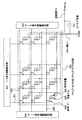
図11に本願発明の保持容量を用いたアクティブマトリクス型液晶表示装置の回路図の一例を示す。ソース信号線駆動回路301、ゲート信号線駆動回路302、アクティブマトリクス回路303、画素TFT304、画素電極と対向電極との間に液晶を挟んだ液晶セル305、画素電極と遮蔽膜の間に誘電体を挟んで形成される保持容量306、ソース信号線307、ゲート信号線308が図11に示されるように設けられている。またカップリング容量310がフローティングになっている遮蔽膜とコモン線との間に設けられている。ソース信号線駆動回路301とゲート信号線駆動回路302は、一般に駆動回路と総称されている。この駆動回路は、アクティブマトリクス回路でなる画素マトリクス部と同一基板上に一体形成されている。
【0105】
また、アクティブマトリクス部303では、ソース信号線駆動回路301に接続されたソース信号線307と、ゲート信号線駆動回路302に接続されたゲート信号線308が交差している。そのソース信号線307とゲート信号線308に囲まれた領域、画素部309に、画素の薄膜トランジスタ(画素TFT)304と、対向電極と画素電極の間に液晶を挟んだ液晶セル305と、保持容量306が設けられている。またコモン線311と遮蔽膜312とが図に示すように設けられている。
【0106】
保持容量306は画素電極と遮蔽膜312の間に誘電体としての酸化膜を挟んだ構成となっており、全ての遮蔽膜312はコモン線311とは接続されていないフローティング(Floating)となっている。
【0107】
またカップリング容量310の容量値は、ゲート信号線1ラインに画素TFTを介して接続されている全ての保持容量の容量値の合計の10倍以上であれば良い。
【0108】
ソース信号線307に入力された画像信号は、画素TFT304により選択され、所定の画素電極に書き込まれる。
【0109】
ソース信号線駆動回路301から出力されたタイミング信号によりサンプリングされた画像信号が、ソース信号線307に供給される。
【0110】
画素TFT304は、ゲート信号線駆動回路302からゲート信号線308を介して入力される選択信号により動作する。
【0111】
ソース信号線に入力される画像信号は、ソース信号線1ラインごとに極性を逆にして印加し、1フレーム期間ごとに信号の極性を反転させることで、液晶に常に1つの向きの電界が印加されることによって液晶が劣化するのを防ぐ。このようにソースライン反転で液晶を駆動させて、遮蔽膜をコモン線に接続せずにフローティングとしている。このような構成にすることで、遮蔽膜をコモン線に接続しなくても、遮蔽膜の電位が時間的に平均を取ると一定に保たれるので、遮蔽膜と画素電極との間に誘電体を挟み込んだ構造の保持容量を形成することが可能になる。よって遮蔽膜をパターニングによって形成した後に、遮蔽膜とコモン線を接続するために、遮蔽膜とコモン線との間に設けられた層間絶縁膜にマスクを用いたフォトリソグラフィーによるコンタクトホールをあける必要がなくなる。このため作製工程を削減し、高い歩留まりを達成することが可能になり、またアクティブマトリクス型液晶表示装置の作製コストを抑えることが可能になる。またそれに加えて、遮蔽膜をフローティングにして遮蔽膜とコモン線との間に大容量のカップリング容量を形成した場合は、遮蔽膜の電位の変動ΔVが小さくなる。カップリング容量の容量値が大きければ大きいほどΔVは小さくなり、遮蔽膜の電位をより一定に保つことが可能になるため、良好なコントラストを得ることができる。
【0112】
図23に図11の上面及び断面の概略図を示す。図23(B)は図23(A)のA−A’における断面図である。
【0113】
ソース信号線駆動回路411(図11に示すところの301)、ゲート信号線駆動回路402、アクティブマトリクス部413(図11に示すところの303)、遮蔽膜404、ITO膜406、コモン線407、FPC414が図23(A)に示すように設けられている。
【0114】
ITO膜406とコモン線407は電気的に接続されており、コモン線407はFPC414によって基板の外部に接続され、一定の電位(基準電位)に保たれている。
【0115】
コモン線407に接続されたITO膜406と遮蔽膜404の重なった部分にカップリング容量416(図11で示すところの310)が形成されている。
【0116】
基板401、ゲート信号線駆動回路402(図11に示すところの302)、層間絶縁膜403、遮蔽膜404(図11に示すところの311)、誘電体405、ITO膜406、コモン線407(図11に示すところの312)、フィラー412、樹脂410、FPCからの引き出し端子上に成膜されたITO膜409、FPCからの引き出し端子408が図23に示すように設けられている。
【0117】
遮蔽膜404とITO膜406と、その間に挟まれた誘電体405とによって、カップリング容量が形成されている。ITO膜406は、ゲート信号線駆動回路402上に設けられており、ゲート信号線駆動回路402の下に設けられたコモン線407と接続している。FPCからの引き出し端子408上にはFPC側のITO膜409が接するように形成されており、FPCからの引き出し端子408上のFPC側のITO膜409とITO膜406とは、フィラー412と樹脂410とによって接続されている。
【0118】
樹脂410は光硬化性の樹脂であっても、熱硬化性の樹脂であっても良く、また光硬化性の樹脂と熱硬化性の樹脂との混合物であっても良い。光硬化性の樹脂と熱硬化性の樹脂との混合物を用いた場合、光によって仮接着の後、熱を加えて圧着させることにより接続する。またフィラーは導電性の材料であることが必要である。大きさの異なるフィラーを2種類以上用いても良く、この場合、サイズの小さいフィラーはスペーサとして働くので導電性でなくても良く、サイズの大きい粒子は電気的に接続させる働きをするので導電性であることが必要である。
【0119】
ITO膜406とコモン線407は電気的に接続されている。コモン線407に接続されているITO膜406と、遮蔽膜404と、その間に設けられた誘電体405によって、図11に示すところのカップリング容量310が形成されている。
【0120】
遮蔽膜をフローティングにして遮蔽膜とコモン線との間に大容量のカップリング容量を形成した場合の画素電位のシミュレーションの結果を図12、図25及び図26を用いて説明する。
【0121】
図12(A)は、遮蔽膜をフローティングにして遮蔽膜とコモン線との間に大容量のカップリング容量を形成したアクティブマトリクス型液晶表示装置にソース線1本おきに白黒の縦縞を表示させたときの、画素電極の電極波形のシミュレーションの結果である。画素数は10×10とし、ゲート信号線側駆動回路上全てに300nFの容量値のカップリング容量を形成したと仮定した。図12(A)は、画面の中央もしくはその隣の画素電極の電極波形の図である。0ms〜16msが1番目の画面を表示したときの画素電位で、16ms〜32msが2番目の画面を表示したときの画素電位である。画素電位は8Vを基準として±5Vの信号を画素電極に印加している。
【0122】
図25は図12のアクティブマトリクス基板のシミュレーションのモデルとなった回路図である。図26は図25における画素部の詳しい回路図である。画素TFT3501、保持容量3502が図26に示すように設けられている。図12に示したシミュレーションは図25におけるpointAの電位を測定したものである。
【0123】
遮蔽膜をフローティングにせずに、低抵抗(1Ω)コモン線(COM)に接続して基準電位に保った場合のシミュレーションの結果を比較のために図12(B)に示す。
【0124】
図12(A)と図12(B)を比較するとほぼ同じシミュレーション結果が得られたことがわかる。つまり、遮蔽膜をコモン線に接続せずにフローティングにし、遮蔽膜とコモン線との間にカップリング容量を設けた場合でも、画素電位の変動は見られず、遮蔽膜をフローティングにせずに、コモン線(COM)に接続して基準電位に保った場合と同程度の画像表示が可能であることがわかった。よって画質を落とすことなく、遮蔽膜とコモン線との間に設けられた層間絶縁膜にマスクを用いたフォトリソグラフィーによってコンタクトホールをあける作製工程を削減し、高い歩留まりを達成することが可能になり、またその作製コストを抑えることが可能になる。
【0125】
(実施例3)
画素マトリクス回路とその周辺に設けられる駆動回路のTFTを同時に作製する方法を、実施例1に示した以外の方法で作製する例について、図13〜図15を用いて説明する。本実施例で開示するプロセスを用いて、本願発明のアクティブマトリクス型表示装置を形成しても良い。
【0126】
〔島状半導体層、ゲート絶縁膜形成の工程:図13(A)〕
図13(A)において、基板7001には、無アルカリガラス基板や石英基板を使用することが望ましい。その他にもシリコン基板や金属基板の表面に絶縁膜を形成したものを基板としても良い。
【0127】
そして、基板7001のTFTが形成される表面には、酸化シリコン膜、窒化シリコン膜、または窒化酸化シリコン膜からなる下地膜をプラズマCVD法やスパッタ法で100〜400nmの厚さに形成した。例えば下地膜として、窒化シリコン膜7002を25〜100nm、ここでは50nmの厚さに、酸化シリコン膜7003を50〜300nm、ここでは150nmの厚さとした2層構造で形成すると良い。下地膜は基板からの不純物汚染を防ぐために設けられるものであり、石英基板を用いた場合には必ずしも設けなくても良い。
【0128】
次に下地膜の上に20〜100nmの厚さの、非晶質シリコン膜を公知の成膜法で形成した。非晶質シリコン膜は含有水素量にもよるが、好ましくは400〜550℃で数時間加熱して脱水素処理を行い、含有水素量を5atom%以下として、結晶化の工程を行うことが望ましい。また、非晶質シリコン膜をスパッタ法や蒸着法などの他の作製方法で形成しても良いが、膜中に含まれる酸素、窒素などの不純物元素を十分低減させておくことが望ましい。ここでは、下地膜と非晶質シリコン膜とは、同じ成膜法で形成することが可能であるので両者を連続形成しても良い。下地膜を形成後、一旦大気雰囲気にさらされないようにすることで表面の汚染を防ぐことが可能となり、作製されるTFTの特性バラツキを低減させることができる。
【0129】
非晶質シリコン膜から結晶質シリコン膜を形成する工程は、公知のレーザー結晶化技術または熱結晶化の技術を用いれば良い。また、シリコンの結晶化を助長する触媒元素を用いて熱結晶化の方法で結晶質シリコン膜を作製しても良い。その他に、微結晶シリコン膜を用いても良いし、結晶質シリコン膜を直接堆積成膜しても良い。さらに、単結晶シリコンを基板上に貼りあわせるSOI(Silicon On Insulators)の公知技術を使用して結晶質シリコン膜を形成しても良い。
【0130】
こうして形成された結晶質シリコン膜の不要な部分をエッチング除去して、島状半導体層7004〜7006を形成した。結晶質シリコン膜のnチャネル型TFTが作製される領域には、しきい値電圧を制御するため、あらかじめ1×10¹⁵〜5×1017cm-3程度の濃度でボロン(B)を添加しておいても良い。
【0131】
次に、島状半導体層7004〜7006を覆って、酸化シリコンまたは窒化シリコンを主成分とするゲート絶縁膜7007を形成した。ゲート絶縁膜7007は、10〜200nm、好ましくは50〜150nmの厚さに形成すれば良い。例えば、プラズマCVD法でN2OとSiH4を原料とした窒化酸化シリコン膜を75nm形成し、その後、酸素雰囲気中または酸素と塩酸の混合雰囲気中、800〜1000℃で熱酸化して115nmのゲート絶縁膜としても良い。(図13(A))
【0132】
〔n-領域の形成:図13(B)〕
島状半導体層7004、7006及び配線を形成する領域の全面と、島状半導体層7005の一部(チャネル形成領域となる領域を含む)にレジストマスク7008〜7011を形成し、n型を付与する不純物元素を添加して低濃度不純物領域7012を形成した。この低濃度不純物領域7012は、後にCMOS回路のnチャネル型TFTに、ゲート絶縁膜を介してゲート電極と重なるLDD領域(本明細書中ではLov領域という。なお、ovとはoverlapの意味である。)を形成するための不純物領域である。なお、ここで形成された低濃度不純物領域に含まれるn型を付与する不純物元素の濃度を(n-)で表すこととする。従って、本明細書中では低濃度不純物領域7012をn-領域と言い換えることができる。
【0133】
ここではフォスフィン(PH3)を質量分離しないでプラズマ励起したイオンドープ法でリンを添加した。望ましければ、質量分離を行うイオンインプランテーション法を用いても良い。この工程では、ゲート絶縁膜7007を通してその下の半導体層にリンを添加した。添加するリン濃度は、5×10¹⁷〜5×10¹⁸atoms/cm3の範囲にするのが好ましく、ここでは1×1018atoms/cm3とした。
【0134】
その後、レジストマスク7008〜7011を除去し、窒素雰囲気中で400〜900℃、好ましくは550〜800℃で1〜12時間の熱処理を行ない、この工程で添加されたリンを活性化する工程を行なった。
【0135】
〔ゲート電極用および配線用導電膜の形成:図13(C)〕
第1の導電膜7013を、タンタル(Ta)、チタン(Ti)、モリブデン(Mo)、タングステン(W)から選ばれた元素またはいずれかを主成分とする導電性材料で、10〜100nmの厚さに形成した。第1の導電膜7013としては、例えば窒化タンタル(TaN)や窒化タングステン(WN)を用いることが望ましい。さらに、第1の導電膜7013上に第2の導電膜7014をTa、Ti、Mo、Wから選ばれた元素またはいずれかを主成分とする導電性材料で、100〜400nmの厚さに形成した。例えば、Taを200nmの厚さに形成すれば良い。また、図示しないが、第1の導電膜7013の下に導電膜7013、7014(特に導電膜7014)の酸化防止のためにシリコン膜を2〜20nm程度の厚さで形成しておくことは有効である。
【0136】
〔p−chゲート電極、配線電極の形成とp++領域の形成:図14(A)〕
レジストマスク7015〜7018を形成し、第1の導電膜と第2の導電膜(以下、積層膜として取り扱う)をエッチングして、pチャネル型TFTのゲート電極7019、ゲート信号線7020、7021を形成した。なお、nチャネル型TFTとなる領域の上には全面を覆うように導電膜7022、7023を残した。
【0137】
そして、レジストマスク7015〜7018をそのまま残してマスクとし、pチャネル型TFTが形成される半導体層7004の一部に、p型を付与する不純物元素を添加する工程を行った。ここではボロンをその不純物元素として、ジボラン(B2H6)を用いてイオンドープ法(勿論、イオンインプランテーション法でも良い)で添加した。ここでは5×10²⁰〜3×10²¹atoms/cm3の濃度にボロンを添加した。なお、ここで形成された不純物領域に含まれるp型を付与する不純物元素の濃度を(p++)で表すこととする。従って、本明細書中では不純物領域7024、7025をp++領域と言い換えることができる。
【0138】
なお、この工程において、レジストマスク7015〜7018を使用してゲート絶縁膜7007をエッチング除去して、島状半導体層7004の一部を露出させた後、p型を付与する不純物元素を添加する工程を行っても良い。その場合、加速電圧が低くて済むため、島状半導体膜に与えるダメージも少ないし、スループットも向上する。
【0139】
〔n―chゲート電極の形成:図14(B)〕
次に、レジストマスク7015〜7018を除去した後、レジストマスク7026〜7029を形成し、nチャネル型TFTのゲート電極7030、7031を形成した。このときゲート電極7030はn-領域7012とゲート絶縁膜を介して重なるように形成した。
【0140】
〔n+領域の形成:図14(C)〕
次に、レジストマスク7026〜7029を除去し、レジストマスク7032〜7034を形成した。そして、nチャネル型TFTにおいて、ソース領域またはドレイン領域として機能する不純物領域を形成する工程を行なった。レジストマスク7034はnチャネル型TFTのゲート電極7031を覆う形で形成した。これは、後の工程において画素マトリクス回路のnチャネル型TFTに、ゲート電極と重ならないようにLDD領域を形成するためである。
【0141】
そして、n型を付与する不純物元素を添加して不純物領域7035〜7039を形成した。ここでも、フォスフィン(PH3)を用いたイオンドープ法(勿論、イオンインプランテーション法でも良い)で行い、この領域のリンの濃度は1×10²⁰〜1×10²¹atoms/cm3とした。なお、ここで形成された不純物領域7037〜7039に含まれるn型を付与する不純物元素の濃度を(n+)で表すこととする。従って、本明細書中では不純物領域7037〜7039をn+領域と言い換えることができる。また、不純物領域7035は既にn-領域が形成されていたので、厳密には不純物領域7037〜7039よりも若干高い濃度でリンを含む。
【0142】
なお、この工程において、レジストマスク7032〜7034およびゲート電極7030をマスクとしてゲート絶縁膜7007をエッチングし、島状半導体膜7005、7006の一部を露出させた後、n型を付与する不純物元素を添加する工程を行っても良い。その場合、加速電圧が低くて済むため、島状半導体膜に与えるダメージも少ないし、スループットも向上する。
【0143】
〔n--領域の形成:図15(A)〕
次に、レジストマスク7032〜7034を除去し、画素マトリクス回路のnチャネル型TFTとなる島状半導体層7006にn型を付与する不純物元素を添加する工程を行った。こうして形成された不純物領域7040〜7043には前記n-領域と同程度かそれより少ない濃度(具体的には5×10¹⁶〜1×10¹⁸atoms/cm3)のリンが添加されるようにした。なお、ここで形成された不純物領域7040〜7043に含まれるn型を付与する不純物元素の濃度を(n--)で表すこととする。従って、本明細書中では不純物領域7040〜7043をn--領域と言い換えることができる。また、この工程ではゲート電極で隠された不純物領域7067を除いて全ての不純物領域にn?の濃度でリンが添加されているが、非常に低濃度であるため無視して差し支えない。
【0144】
〔熱活性化の工程:図15(B)〕
次に、後に第1の層間絶縁膜の一部となる保護絶縁膜7044を形成した。保護絶縁膜7044は窒化シリコン膜、酸化シリコン膜、窒化酸化シリコン膜またはそれらを組み合わせた積層膜で形成すれば良い。また、膜厚は100〜400nmとすれば良い。
【0145】
その後、それぞれの濃度で添加されたn型またはp型を付与する不純物元素を活性化するために熱処理工程を行った。この工程はファーネスアニール法、レーザーアニール法、またはラピッドサーマルアニール法(RTA法)で行うことができる。ここではファーネスアニール法で活性化工程を行った。加熱処理は、窒素雰囲気中において300〜650℃、好ましくは400〜550℃、ここでは450℃、2時間の熱処理を行った。
【0146】
さらに、3〜100%の水素を含む雰囲気中で、300〜450℃で1〜12時間の熱処理を行い、島状半導体層を水素化する工程を行った。この工程は熱的に励起された水素により半導体層のダングリングボンドを終端する工程である。水素化の他の手段として、プラズマ水素化(プラズマにより励起された水素を用いる)を行っても良い。
【0147】
〔層間絶縁膜、ソース/ドレイン電極、遮蔽膜、画素電極、保持容量の形成:図15(C)〕
活性化工程を終えたら、保護絶縁膜7044の上に0.5〜1.5μm厚の層間絶縁膜7045を形成した。前記保護絶縁膜7044と層間絶縁膜7045とでなる積層膜を第1の層間絶縁膜とした。
【0148】
その後、それぞれのTFTのソース領域またはドレイン領域に達するコンタクトホールが形成され、ソース電極7046〜7048と、ドレイン電極7049、7050を形成した。図示していないが、本実施例ではこの電極を、Ti膜を100nm、Tiを含むアルミニウム膜300nm、Ti膜150nmをスパッタ法で連続して形成した3層構造の積層膜とした。
【0149】
次に、パッシベーション膜7051として、窒化シリコン膜、酸化シリコン膜、または窒化酸化シリコン膜で50〜500nm(代表的には200〜300nm)の厚さで形成した。その後、この状態で水素化処理を行うとTFTの特性向上に対して好ましい結果が得られた。例えば、3〜100%の水素を含む雰囲気中で、300〜450℃で1〜12時間の熱処理を行うと良く、あるいはプラズマ水素化法を用いても同様の効果が得られた。なお、ここで後に画素電極とドレイン電極を接続するためのコンタクトホールを形成する位置において、パッシベーション膜7051に開口部を形成しておいても良い。
【0150】
その後、有機樹脂からなる第2の層間絶縁膜7052を約1μmの厚さに形成した。有機樹脂としては、ポリイミド、アクリル、ポリアミド、ポリイミドアミド、BCB(ベンゾシクロブテン)等を使用することができる。有機樹脂膜を用いることの利点は、成膜方法が簡単である点や、比誘電率が低いので、寄生容量を低減できる点、平坦性に優れる点などが上げられる。なお上述した以外の有機樹脂膜や有機系SiO化合物などを用いることもできる。ここでは、基板に塗布後、熱重合するタイプのポリイミドを用い、300℃で焼成して形成した。
【0151】
次に、画素マトリクス回路となる領域において、第2の層間絶縁膜7052上に遮蔽膜7053を形成した。遮蔽膜7053はアルミニウム(Al)、チタン(Ti)、タンタル(Ta)から選ばれた元素またはいずれかを主成分とする膜で100〜300nmの厚さに形成した。そして、遮蔽膜7054の表面に陽極酸化法またはプラズマ酸化法により30〜150nm(好ましくは50〜75nm)の厚さの酸化膜7054を形成した。ここでは遮蔽膜7053としてアルミニウム膜またはアルミニウムを主成分とする膜を用い、誘電体7054として酸化アルミニウム膜(アルミナ膜)を用いた。
【0152】
なお、ここでは遮蔽膜の表面のみに絶縁膜を設ける構成としたが、絶縁膜をプラズマCVD法、熱CVD法またはスパッタ法などの気相法によって形成しても良い。その場合も膜厚は30〜150nm(好ましくは50〜75nm)とすることが好ましい。また、酸化シリコン膜、窒化シリコン膜、窒化酸化シリコン膜、DLC(Diamond like carbon)膜または有機樹脂膜を用いても良い。さらに、これらを組み合わせた積層膜を用いても良い。
【0153】
次に、第2の層間絶縁膜7052にドレイン電極7050に達するコンタクトホールを形成し、画素電極7055を形成した。なお、画素電極7056、7057はそれぞれ隣接する別の画素の画素電極である。画素電極7055〜7057は、透過型液晶表示装置とする場合には透明導電膜を用い、反射型の液晶表示装置とする場合には金属膜を用いれば良い。ここでは透過型の液晶表示装置とするために、酸化インジウム・スズ(ITO)膜を100nmの厚さにスパッタ法で形成した。
【0154】
また、この時、画素電極7055と遮蔽膜7053とが酸化膜7054を介して重なった領域7058が保持容量を形成した。
【0155】
こうして同一基板上に、ドライバー回路となるCMOS回路と画素マトリクス回路とを有したアクティブマトリクス基板が完成した。なお、ドライバー回路となるCMOS回路にはpチャネル型TFT7081、nチャネル型TFT7082が形成され、画素マトリクス回路にはnチャネル型TFTでなる画素TFT7083が形成された。
【0156】
CMOS回路のpチャネル型TFT7081には、チャネル形成領域7061、ソース領域7062、ドレイン領域7063がそれぞれp+領域で形成された。また、nチャネル型TFT7082には、チャネル形成領域7064、ソース領域7065、ドレイン領域7066、ゲート絶縁膜を介してゲート電極と重なったLDD領域(以下、Lov領域という。なお、ovとはoverlapの意である。)7067が形成された。この時、ソース領域7065、ドレイン領域7066はそれぞれ(n-+n+)領域で形成され、Lov領域7067はn-領域で形成された。
【0157】
また、画素TFT7083には、チャネル形成領域7068、7069、ソース領域7070、ドレイン領域7071、ゲート絶縁膜を介してゲート電極と重ならないLDD領域(以下、Loff領域という。なお、offとはoffsetの意である。)7072〜7075、Loff領域7073、7074に接したn+領域7076が形成された。この時、ソース領域7070、ドレイン領域7071はそれぞれn+領域で形成され、Loff領域7072〜7075はn--領域で形成された。
【0158】
また、チャネル長3〜7μmに対してLov領域の長さ(幅)は0.5〜3.0μm、代表的には1.0〜1.5μmとすれば良い。また、画素TFT7083に設けられるLoff領域7072〜7075の長さ(幅)は0.5〜3.5μm、代表的には2.0〜2.5μmとすれば良い。
【0159】
図28に、コモン線と、FPCからの引き出し端子との接合部分を示す。基板7001、図15(C)に示したnチャネル型TFTを有するゲート信号線駆動回路2902、コモン線2903、遮蔽膜2904、誘電体2905、ITO膜2906、フィラー2907、樹脂2908、FPCからの引き出し端子上に成膜されたITO膜2909、FPCからの引き出し端子2910が図28に示すように設けられている。
【0160】
遮蔽膜2904とITO膜2906と、その間に挟まれた誘電体2905とによって、カップリング容量が形成されている。ITO膜2906は、ゲート信号線駆動回路2902上に設けられており、ゲート信号線駆動回路2902の下に設けられたコモン線2903と接続している。FPCからの引き出し端子2910上にはFPC側のITO膜2909が接するように形成されており、FPCからの引き出し端子2910上のFPC側のITO膜2909とITO膜2906とは、フィラー2907と樹脂2908とによって接続されている。
【0161】
樹脂2908は光硬化性の樹脂であっても、熱硬化性の樹脂であっても良く、また光硬化性の樹脂と熱硬化性の樹脂との混合物であっても良い。光硬化性の樹脂と熱硬化性の樹脂との混合物を用いた場合、光によって仮接着の後、熱を加えて圧着させることにより接続する。またフィラーは導電性の材料であることが必要である。大きさの異なるフィラーを2種類以上用いても良く、この場合、サイズの小さいフィラーはスペーサとして働くので導電性でなくても良く、サイズの大きい粒子は電気的に接続させる働きをするので導電性であることが必要である。
【0162】
本願発明では、ソースライン反転によって液晶を駆動してやり、かつ遮蔽膜を一定の電位(基準電位)に保たれたコモン線に接続しない。ソースライン反転によって、遮蔽膜の電位は時間的に平均を取ると一定に保たれるので、遮蔽膜と画素電極との間に誘電体を挟み込んだ構造の保持容量において、遮蔽膜をフローティングにすることが可能になる。よって遮蔽膜をパターニングによって形成した後に、遮蔽膜とコモン線とを接続するために、遮蔽膜とコモン線との間に設けられた層間絶縁膜にマスクを用いたフォトリソグラフィーによるコンタクトホールをあける必要がなくなる。このため作製工程を削減し、高い歩留まりを達成することが可能になり、またアクティブマトリクス型液晶表示装の作製コストを抑えることが可能になる。
【0163】
(実施例4)
上述の実施例1〜3で説明した本願発明の液晶表示装置は、図16に示すような3板式のプロジェクタに用いることができる。
【0164】
図16において、2401は白色光源、2402〜2405はダイクロイックミラー、2406ならびに2407は全反射ミラー、2408〜2410は本願発明の液晶表示装置、および2411は投影レンズである。
【0165】
(実施例5)
また、上述の実施例1〜3で説明した本願発明の液晶表示装置は、図17に示すような3板式のプロジェクタに用いることもできる。
【0166】
図17において、2501は白色光源、2502ならびに2503はダイクロイックミラー、2504〜2506は全反射ミラー、2507〜2509は本願発明の液晶表示装置、および2510はダイクロイックプリズム、および2511は投影レンズである。
【0167】
(実施例6)
また、上述の実施例1〜3で説明した本願発明の液晶表示装置は、図18に示すような単板式のプロジェクタに用いることもできる。
【0168】
図18において、2601はランプとリフレクターとから成る白色光源である。2602、2603、および2604は、ダイクロイックミラーであり、それぞれ青、赤、緑の波長領域の光を選択的に反射する。2605はマイクロレンズアレイであり、複数のマイクロレンズによって構成されている。2606は本願発明の液晶表示装置である。2607はフィールドレンズ、2608は投影レンズ、2609はスクリーンである。
【0169】
(実施例7)
上記実施例5〜7のプロジェクタは、その投影方法によってリアプロジェクターとフロントプロジェクターとがある。
【0170】
図19(A)はフロント型プロジェクタ−であり、本体10001、本願発明の液晶表示装置10002、光源10003、光学系10004、スクリーン10005で構成されている。なお、図19(A)には、液晶表示装置を1つ組み込んだフロントプロジェクターが示されているが、液晶表示装置を3つ(R、G、Bの光にそれぞれ対応させる)組み込むことによって、より高解像度・高精細のフロント型プロジェクタを実現することができる。
【0171】
図19(B)はリア型プロジェクターであり、10006は本体、10007は液晶表示装置であり、10008は光源であり、10009はリフレクター、10010はスクリーンである。なお、図19(B)には、アクティブマトリクス型半導体表示装置を3つ(R、G、Bの光にそれぞれ対応させる)組み込んだリア型プロジェクタが示されている。
【0172】
(実施例8)
本実施例では、本願発明の液晶表示装置をゴーグル型ディスプレイに用いた例を示す。
【0173】
図20を参照する。2801はゴーグル型ディスプレイ本体である。2802−Rならびに2802−Lは本願発明の液晶表示装置であり、2803−Rならびに2803−LはLEDバックライトであり、2804−Rならびに2804−Lは光学素子である。
【0174】
(実施例9)
本願発明の液晶表示装置には他に様々な用途がある。本実施例では、本願発明の液晶表示装置を組み込んだ半導体装置について説明する。
【0175】
このような半導体装置には、ビデオカメラ、スチルカメラ、カーナビゲーション、パーソナルコンピュータ、携帯情報端末(モバイルコンピュータ、携帯電話など)などが挙げられる。それらの一例を図21に示す。
【0176】
図21(A)は携帯電話であり、本体11001、音声出力部11002、音声入力部11003、本願発明の液晶表示装置11004、操作スイッチ11005、アンテナ11006で構成される。
【0177】
図21(B)はビデオカメラであり、本体12007、本願発明の液晶表示装置12008、音声入力部12009、操作スイッチ12010、バッテリー12011、受像部12012で構成される。
【0178】
図21(C)はモバイルコンピュータであり、本体13001、カメラ部13002、受像部13003、操作スイッチ13004、本願発明の液晶表示装置1305で構成される。
【0179】
図21(D)は携帯書籍(電子書籍)であり、本体14001、本願発明の液晶表示装置14002、14003、記憶媒体14004、操作スイッチ14005、アンテナ14006で構成される。
【0180】
(実施例10)
【0181】
本実施例においては、本願発明の液晶表示装置をノートブック型パーソナルコンピュータに用いた例を図22に示す。
【0182】
3001はノートブック型パーソナルコンピュータ本体であり、3002は本願発明の液晶表示装置である。また、バックライトにはLEDが用いられている。なお、バックライトに従来のように陰極管を用いても良い。
【0183】
(実施例11)
本実施例では、遮蔽膜をアクティブマトリクス部を有するアクティブマトリクス基板上だけではなく、対向基板上にも設ける例について説明する。
【0184】
基板(アクティブマトリクス基板)501、ソース信号線駆動回路511、ゲート信号線駆動回路502、アクティブマトリクス部513、遮蔽膜504、ITO膜506、コモン線507、FPC514が図24(A)に示すように設けられている。また対向基板上に設けられた対向遮蔽膜517が図に示すようにソース信号線駆動回路511全体と重なっており、遮蔽膜504と一部重なっている。この実施例では対向遮蔽膜504をソース信号線駆動回路511全体と重なるように、対向基板上に設けたが、ソース信号線駆動回路が有するサンプリング回路のみと重なるようにしても良い。
【0185】
ITO膜506とコモン線507は電気的に接続されており、コモン線507はFPC514によって基板の外部に接続され、一定の電位(基準電位)に保たれている。
【0186】
コモン線507に接続されたITO膜506と遮蔽膜504の重なった部分にカップリング容量516が形成されている。
【0187】
対向遮蔽膜517と遮蔽膜504の重なっている部分(重複部)518は、外部からの光がソース信号線駆動回路511に入射するのを防ぐ。光がソース信号線駆動回路511、特にソース信号線駆動回路が有するサンプリング回路に入射すると、サンプリング回路を構成する薄膜トランジスタ(TFT)のオフ電流が増加してしまい、ノイズの原因となる。対向遮蔽膜517は、Tiを有していることが望ましく、Tiを有することで光が対向遮蔽膜517に反射してソース信号線駆動回路に入射するのを防ぐ。また重複部518を20μm以上設けることが、ソース信号線駆動回路511への光の入射を防ぐのに効果的である。
【0188】
図24(B)に、図24(A)のA−A’における断面図を示す。基板501、アクティブマトリクス部513、層間絶縁膜512、遮蔽膜504、誘電体505、対向基板521、対向基板側層間絶縁膜522、対向基板側遮蔽膜517が図に示すように設けられている。基板501と対向基板521はスペーサ(図示せず)を挟んで、シール材(図示せず)により接着される。遮蔽膜504と対向基板側遮蔽膜517は一部重なっており、この重なりの幅Lは20μm以上あることが好ましい。
【0189】
また、アクティブマトリクス基板上の回路は、実施例1〜3と同様の方法で作製すれば良い。また以下の実施例で開示される方法を用いても良い。
【0190】
(実施例12)
本願発明の画素マトリクス回路とその周辺に設けられる駆動回路のTFTを同時に作製する実施例1に示した以外の方法の一例について、図29を用いて説明する。なお、本願発明はこの作製方法に限られない。
【0191】
実施例1の図8(C)の工程まで同様に形成する。次にレジストマスクを用いて、第1の導電膜と第2の導電膜(以下、積層膜として取り扱う)をエッチングして、pチャネル型TFTのゲート電極8001、nチャネル型TFTのゲート電極8002、ゲート信号線8003a、8003bを形成した。このときゲート電極8002はn-領域6012、6013とゲート絶縁膜を介して重なるようにした。(図29(A))
【0192】
そして、pチャネル型TFTのゲート電極8001、nチャネル型TFTのゲート電極8002、ゲート信号線8003a、8003bをそれぞれマスクとして、n型を付与する不純物を添加した。こうして形成された不純物領域8004、8005、8006、8007、8008には、図8(B)で示した前記n-領域と同程度かそれより少ない濃度(具体的には5×10¹⁶〜1×10¹⁸atoms/cm3)のリンが添加されるようにした。なお、ここで形成された不純物領域8004〜8008に含まれるn型を付与する不純物元素の濃度を(n--)で表すこととする。従って、本明細書中では不純物領域8004〜8008をn--領域と言い換えることができる。また、この工程ではゲート電極で隠された不純物領域8009、8010を除いて全ての不純物領域にn?の濃度でリンが添加されているが、非常に低濃度であるため無視して差し支えない。(図29(B))
【0193】
次に、レジストマスク8011〜8014を形成した。そして、nチャネル型TFTにおいて、ソース領域またはドレイン領域として機能する不純物領域を形成する工程を行なった。レジストマスク8012はnチャネル型TFTのゲート電極8002を覆う形で形成した。これは、後の工程において画素マトリクス回路のnチャネル型TFTに、ゲート電極と重ならないようにLDD領域を形成するためである。
【0194】
そして、n型を付与する不純物元素を添加して不純物領域8016〜8022を形成した。ここでも、フォスフィン(PH3)を用いたイオンドープ法(勿論、イオンインプランテーション法でも良い)で行い、この領域のリンの濃度は1×10²⁰〜1×10²¹atoms/cm3とした。なお、ここで形成された不純物領域8018〜8022に含まれるn型を付与する不純物元素の濃度を(n+)で表すこととする。従って、本明細書中では不純物領域8018〜8022をn+領域と言い換えることができる。また、不純物領域8009、8010は既にn-領域が形成されていたので、厳密には不純物領域8020〜8022よりも若干高い濃度でリンを含む。(図29(C))
【0195】
なお、この工程において、レジストマスク8011〜8014をマスクとしてゲート絶縁膜6007をエッチングし、島状半導体膜6005、6006の一部を露出させた後、n型を付与する不純物元素を添加する工程を行っても良い。その場合、加速電圧が低くて済むため、島状半導体膜に与えるダメージも少ないし、スループットも向上する。
【0196】
レジストマスク8024を、nチャネル型TFTとなる領域の上全面を覆うように形成した。そして、レジストマスク8024をマスクとし、pチャネル型TFTが形成される半導体層6004の一部に、p型を付与する不純物元素を添加する工程を行った。ここではボロンをその不純物元素として、ジボラン(B2H6)を用いてイオンドープ法(勿論、イオンインプランテーション法でも良い)で添加した。ここでは5×10²⁰〜3×10²¹atoms/cm3の濃度にボロンを添加した。なお、ここで形成された不純物領域に含まれるp型を付与する不純物元素の濃度を(p+)で表すこととする。従って、本明細書中では不純物領域8025、8026をp+領域と言い換えることができる。(図29(D))
【0197】
なお、この工程において、レジストマスク8024を使用してゲート絶縁膜6007をエッチング除去して、島状半導体層6004の一部を露出させた後、p型を付与する不純物元素を添加する工程を行っても良い。その場合、加速電圧が低くて済むため、島状半導体膜に与えるダメージも少ないし、スループットも向上する。
【0198】
次に、添加された不純物元素(リンまたはボロン)の活性化工程を行う。本実施例ではこの活性化工程をファーネスアニールまたはランプアニールによって行うことが好ましい。ファーネスアニールを用いる場合、450〜650℃、好ましくは500〜550℃、ここでは500℃、4時間の熱処理を行うことにする。(図29(E))
【0199】
本実施例の場合、nチャネル型TFTおよびpチャネル型TFTの双方のソース領域またはドレイン領域に、必ずn+領域に相当する濃度のリンが含まれた領域を有する。そのため、熱活性化のための熱処理工程において、リンによるニッケルのゲッタリング効果を得ることができる。即ち、チャネル形成領域から矢印で示す方向へニッケルが移動し、ソース領域またはドレイン領域に含まれるリンの作用によってゲッタリングされる。これは特に結晶化を促進させる金属、例えばニッケルを用いた場合に有効である。
【0200】
このように本実施例を実施すると、島状半導体膜に添加された不純物元素の活性化工程と、結晶化に用いた触媒元素のゲッタリング工程とを兼ねることができ、工程の簡略化に有効である。
【0201】
そして実施例1で上述したように、図10(C)に示したのと同様の工程で、画素マトリクス回路とその周辺に設けられる駆動回路のTFTを完成する。なお、本実施例で示した作製工程は一例であり、作製工程の順序は本実施例の形態に限られない。
【0202】
(実施例13)
本実施例では、本願発明のアクティブマトリクス回路の断面図及び上面図の、図23で示したものとは別の例について説明する。図30に図11の上面及び断面の概略図を示す。図30(A)は本願発明のアクティブマトリクス回路の上面図である。
【0203】
基板601に、ソース信号線駆動回路611(図11に示すところの301)、ゲート信号線駆動回路602(図11に示すところの302)、アクティブマトリクス部613(図11に示すところの303)、遮蔽膜604、ITO膜606、コモン線607、FPC614が図30(A)に示すように設けられている。
【0204】
ITO膜606とコモン線607は、接続部608において電気的に接続しており、コモン線607はFPC614によって基板の外部に接続され、一定の電位(基準電位)に保たれている。
【0205】
コモン線607に接続されたITO膜606と遮蔽膜604の重なった部分にカップリング容量616(図11で示すところの310)が形成されている。本実施例においてITO膜606はゲート信号線駆動回路602の一部を覆うように形成されているため、容量値の大きいカップリング容量616を形成することが可能である。なおITO膜606をゲート信号線駆動回路602全体を覆うように形成しても良い。
【0206】
図30(B)は、図30(A)のA−A’における断面図である。基板601、ゲート信号線駆動回路602が有するnチャネル型TFTの1つ616、層間絶縁膜617、遮蔽膜604(図11に示すところの311)、誘電体605、ITO膜606、コモン線607(図11に示すところの312)、フィラー612、樹脂610、FPCからの引き出し端子上に成膜されたITO膜609、FPCからの引き出し端子615が図30(B)に示すように設けられている。
【0207】
遮蔽膜604とITO膜606と、その間に挟まれた誘電体605とによって、カップリング容量が形成されている。ITO膜606は、ゲート信号線駆動回路602上に設けられており、言い換えると、ゲート信号線駆動回路602が有するnチャネル型TFTの1つ616の上に設けられている。
【0208】
またITO膜606は、基板601上に設けられたコモン線607と、接続部608において接続している。なお本実施例ではITO膜606とコモン線607とを直接接続しているが、別の配線等を間に介して接続することにより、ITO膜606とコモン線607とを電気的に接続しても良いことは言うまでもない。
【0209】
FPCからの引き出し端子615上にはFPC側のITO膜609が接するように形成されており、FPCからの引き出し端子615上のFPC側のITO膜609とITO膜606とは、フィラー612と樹脂610とによって接続されている。
【0210】
樹脂610は光硬化性の樹脂であっても、熱硬化性の樹脂であっても良く、また光硬化性の樹脂と熱硬化性の樹脂との混合物であっても良い。光硬化性の樹脂と熱硬化性の樹脂との混合物を用いた場合、光によって仮接着の後、熱を加えて圧着させることにより接続する。またフィラーは導電性の材料であることが必要である。大きさの異なるフィラーを2種類以上用いても良く、この場合、サイズの小さいフィラーはスペーサとして働くので導電性でなくても良く、サイズの大きい粒子は電気的に接続させる働きをするので導電性であることが必要である。
【0211】
本実施例のアクティブマトリクス回路と駆動回路は、これまでの実施例で開示した方法を用いて作製することが可能である。
【0212】
(実施例14)
本実施例では、本願発明を用いた電気光学装置のうち、図16〜図22で示した以外のものについて、その一例を図31に示す。
【0213】
図31(A)はディスプレイであり、筐体2001、支持台2002、表示部2003等を含む。本願発明は表示部2003に適用することができる。
【0214】
図31(B)は頭部取り付け型のディスプレイの一部(右片側)であり、本体2201、信号ケーブル2202、頭部固定バンド2203、スクリーン部2204、光学系2205、表示部2206等を含む。本願発明は表示部2206に適用できる。
【0215】
図31(C)はプログラムを記録した記録媒体(以下、記録媒体と呼ぶ)を用いるプレーヤーであり、本体2301、表示部2302、スピーカ部2303、記録媒体2304、操作スイッチ2305で構成される。なお、この装置は記録媒体としてDVD(Digital Versatile Disc)、CD等を用い、音楽鑑賞や映画鑑賞やゲームやインターネットを行うことができる。本願発明は表示部2302に適用することができる。
【0216】
以上の様に、本願発明の適用範囲は極めて広く、あらゆる分野の電子機器に適用することが可能である。また、本実施例の電子機器は実施例1〜3、11〜13のどのような組み合わせからなる構成を用いても実現することができる。
【0217】
【発明の効果】
ソースライン反転で液晶を駆動させて、遮蔽膜をコモン線に接続せずにフローティングとしている。このような構成にすることで、遮蔽膜をコモン線に接続しなくても、遮蔽膜の電位が時間的に平均を取ると一定に保たれるので、遮蔽膜と画素電極との間に誘電体を挟み込んだ構造の保持容量を形成することが可能になる。よって遮蔽膜をパターニングによって形成した後に、遮蔽膜とコモン線を接続するために、遮蔽膜とコモン線との間に設けられた層間絶縁膜にマスクを用いたフォトリソグラフィーによるコンタクトホールをあける必要がなくなる。このため作製工程を削減し、高い歩留まりを達成することが可能になり、またアクティブマトリクス型液晶表示装の作製コストを抑えることが可能になる。またそれに加えて、遮蔽膜をフローティングにして遮蔽膜とコモン線との間に大容量のカップリング容量を形成した場合は、遮蔽膜の電位をさらに一定に保つことが可能になるため、良好なコントラストを得ることができる。
【0218】
なお、上記実施例はTFTの活性層として珪素膜を例にとって説明したが、必要に応じて不純物を添加したり、Si−Ge化合物など、他の半導体を用いても良い。また画素が有するTFTとして、ダブルゲート構造を有するTFTを示したが、シングルゲート構造を有していても良いし、他のマルチゲート構造を有していても良い。また画素が有するTFTの活性層が、a−Si(アモルファスシリコン)を有していても良い。
【図面の簡単な説明】
【図1】 本願発明のアクティブマトリクス回路の回路図。
【図2】 本願発明の画素マトリクス回路の上面構造を示す図。
【図3】 本願発明の画素マトリクス回路の上面構造を示す図。
【図4】 ソースライン反転の概念を示す図。
【図5】 ソース信号線駆動回路のブロック図。
【図6】 ソース信号線駆動回路の回路図。
【図7】 アナログスイッチとレベルシフト回路の等価回路図。
【図8】 本願発明のTFTの作製工程を示す断面図。
【図9】 本願発明のTFTの作製工程を示す断面図。
【図10】 本願発明のTFTの作製工程を示す断面図。
【図11】 本願発明のアクティブマトリクス回路の回路図。
【図12】 本願発明のシミュレーション結果を示す図。
【図13】 本願発明のTFTの作製工程を示す断面図。
【図14】 本願発明のTFTの作製工程を示す断面図。
【図15】 本願発明のTFTの作製工程を示す断面図。
【図16】 本願発明の液晶表示装置を用いた3板式プロジェクタの概略構成図。
【図17】 本願発明の液晶表示装置を用いた3板式プロジェクタの概略構成図。
【図18】 本願発明の液晶表示装置を用いた単板式プロジェクタの概略構成図。
【図19】 本願発明の液晶表示装置を用いたフロントプロジェクタおよびリアプロジェクタの概略構成図。
【図20】 本願発明の液晶表示装置を用いたゴーグル型ディスプレイの概略構成図。
【図21】 本願発明の液晶表示装置を用いた電子機器の例。
【図22】 本願発明の液晶表示装置を用いたノートブック型パーソナルコンピュータの概略構成図。
【図23】 本願発明のアクティブマトリクス回路の断面図及び上面図。
【図24】 本願発明のアクティブマトリクス回路の上面図。
【図25】 アクティブマトリクス基板のシミュレーションのモデルとなる回路図。
【図26】 アクティブマトリクス基板のシミュレーションのモデルとなる回路における画素部の回路図。
【図27】 ゲート信号線駆動回路上に設けられたITOに接続されたコモン線と、FPCの取り出し端子との接合部分の断面図。
【図28】 ゲート信号線駆動回路上に設けられたITOに接続されたコモン線と、FPCの取り出し端子との接合部分の断面図。
【図29】 本願発明のTFTの作製工程を示す断面図。
【図30】 本願発明のアクティブマトリクス回路の断面図及び上面図。
【図31】 本願発明の液晶表示装置を用いた電子機器の例。
【符号の説明】
11 ソース信号線駆動回路
12 ゲート信号線駆動回路
13 アクティブマトリクス部
14 画素TFT
15 液晶
16 保持容量
17 ソース信号線
18 ゲート信号線
19 画素部[0001]
BACKGROUND OF THE INVENTION
The present invention relates to a semiconductor device having a circuit formed of a thin film transistor (hereinafter referred to as TFT) on a substrate having an insulating surface, and a manufacturing method thereof. In particular, the present invention relates to an electro-optical device typified by a liquid crystal display device in which a pixel matrix circuit and a drive circuit provided around the pixel matrix circuit are provided on the same substrate, and an electronic apparatus equipped with the electro-optical device. Note that in this specification, a semiconductor device refers to all devices that function by utilizing semiconductor characteristics, and the above-described electro-optical device and an electronic apparatus including the electro-optical device are also included in the semiconductor device.
[0002]
[Prior art]
Recently, a technique for manufacturing a thin film transistor (TFT) on an inexpensive glass substrate has been rapidly developed. The reason is that the demand for active matrix liquid crystal display devices has increased. In an active matrix liquid crystal display device, a thin film transistor is disposed in each of several tens to several millions of pixels arranged in a matrix, and charges entering and exiting each pixel electrode are controlled by a switching function of the thin film transistor. .
[0003]
Liquid crystal is sandwiched between each pixel electrode and the counter electrode to form a kind of capacitor. Therefore, by controlling the flow of electric charges into and out of the capacitor with the thin film transistor, the electro-optical characteristics of the liquid crystal can be changed, and the light transmitted through the liquid crystal panel can be controlled to display an image. In addition, since the holding voltage of the capacitor having such a configuration gradually decreases due to current leakage, the electro-optical characteristics of the liquid crystal change and the contrast of image display is deteriorated.
[0004]
Therefore, it is common to install another capacitor called a holding capacitor in series with a capacitor composed of liquid crystal, and to supply the charge lost due to leakage or the like to the capacitor composed of liquid crystal.
[0005]
Although the storage capacitor has various structures, a structure in which an oxide film as a dielectric is sandwiched between the shielding film and the pixel electrode can be given. The shielding film is a film having a light shielding property for preventing the thin film transistor from changing its conductivity due to light irradiation in the pixel matrix portion of the transmissive liquid crystal display device.
[Problems to be solved by the invention]
A storage capacitor having a structure in which a dielectric is sandwiched between the shielding film and the pixel electrode is connected to a common line to which a reference potential is applied in order to keep the shielding film at a constant potential.
[0006]
Therefore, in the process, after forming the shielding film by patterning, it is necessary to open a contact hole in the interlayer insulating film provided between the shielding film and the common line in order to connect the shielding film and the common line. The contact hole is formed by photolithography using a mask.
[0007]
An active matrix type liquid crystal display device uses, for example, an active layer forming step in addition to a step of forming a contact hole in an interlayer insulating film provided between a shielding film and a common line by photolithography using a mask in the manufacturing process. , A gate insulating film forming step, a pixel electrode forming step, a gate line and source signal line forming step, and the like. Photolithography using a mask is a factor that increases the number of manufacturing steps of an active matrix liquid crystal display device, and it has been desired to reduce the number of manufacturing steps in order to achieve a high yield.
[0008]
[Means for Solving the Problems]
In an active matrix liquid crystal display device, a driving method in which a voltage having an opposite polarity is applied to a source signal line connected to a pixel TFT is called source line inversion. The source line inversion is performed in order to prevent the liquid crystal from being deteriorated by always applying an electric field in one direction to the liquid crystal. As shown in FIG. 4, by applying a signal having a reverse polarity for each source signal line and inverting the polarity of the signal for each frame period, an electric field in one direction is always applied to the liquid crystal. Prevents the liquid crystal from deteriorating. One frame period indicates a period during which all pixels display one screen.
[0009]
When this source line inversion is used, fluctuations in the potential of the shielding film are also averaged. For this reason, even if the shielding film is not connected to a common line maintained at a constant potential (reference potential), the potential of the shielding film is kept almost constant when taking an average over time. In a storage capacitor having a structure in which a dielectric is sandwiched between electrodes, the shielding film can be made floating. Therefore, after forming the shielding film by patterning, in order to connect the shielding film and the common line, it is necessary to open a contact hole by photolithography using a mask in the interlayer insulating film provided between the shielding film and the common line Disappears. Therefore, the manufacturing process of the active matrix liquid crystal display device can be reduced, a high yield can be achieved, and the manufacturing cost can be suppressed.
[0010]
In addition to the above configuration, when a large-capacity coupling capacitor is formed between the shielding film and the common line, the fluctuation ΔV of the potential of the shielding film is reduced. ΔV is determined by the capacitance value C of the coupling capacitance formed between the shielding film and the common line and the charge amount Q applied to the shielding film. However, since the charge amount Q is fixed by the number of pixels and the voltage value of the signal input to the source signal line, the value of the fluctuation ΔV of the shielding film is actually determined by the capacitance value C of the coupling capacitor. Will be. The larger the value of C, the smaller ΔV, and the potential of the shielding film can be kept more constant.
[0011]
When the shielding film is floating and a large-capacity coupling capacitor is formed between the shielding film and the common line, it is provided between the shielding film and the common line as in the above-described configuration in which the shielding film is only floated. There is no need to make a contact hole by photolithography using a mask for the formed interlayer insulating film. The capacitance value of the coupling capacitor may be 10 times or more of the total capacitance value of all the storage capacitors connected to one line of the gate signal line via the pixel TFT. Therefore, manufacturing steps of the active matrix liquid crystal display device can be reduced, high yield can be achieved, and manufacturing costs can be reduced. In addition, in the case where the shielding film is floated and a large-capacity coupling capacitor is formed between the shielding film and the common line, the potential of the shielding film can be kept more constant. Contrast can be obtained.
[0012]
The configuration of the present invention will be described below.
[0013]
According to an embodiment of the present invention, there is provided an active matrix liquid crystal display device having a substrate provided with a plurality of pixel TFTs, a pixel electrode electrically connected to the pixel TFTs, and a shielding film,
The shielding film is floating,
There is provided an active matrix liquid crystal display device having a dielectric between the pixel electrode and the shielding film. This achieves the above object.
[0014]
According to an embodiment of the present invention, a plurality of source signal lines, a plurality of gate signal lines, a plurality of pixel TFTs, a pixel electrode electrically connected to the pixel TFT, and a shielding film are provided. An active matrix type liquid crystal display device having a manufactured substrate,
The plurality of pixel TFTs are electrically connected to the source signal line and the gate signal line,
The shielding film is floating,
A dielectric is provided between the pixel electrode and the shielding film,
An active matrix, wherein a signal having a reverse polarity is applied to each of the plurality of source signal lines, and the polarity of the signal applied to each of the plurality of source signal lines is inverted every frame period. A liquid crystal display device is provided. This achieves the above object.
[0015]
According to an embodiment of the present invention, a first substrate provided with a plurality of source signal lines, a plurality of gate signal lines, a plurality of pixel TFTs, a pixel electrode, and a shielding film;
A second substrate provided with a counter electrode;
A liquid crystal sandwiched between the pixel electrode and the counter electrode;
In an active matrix liquid crystal display device having
Each of the pixel TFTs includes a gate electrode, a gate insulating film, an active layer having a source region, a drain region, and a channel formation region,
The gate electrode is connected to the gate signal line;
The source region or drain region is connected to the source signal line;
The drain region or the source region is connected to the pixel electrode;
A dielectric is provided between the pixel electrode and the shielding film,
The shielding film is floating,
An active matrix, wherein a signal having a reverse polarity is applied to each of the plurality of source signal lines, and the polarity of the signal applied to each of the plurality of source signal lines is inverted every frame period. A liquid crystal display device is provided. This achieves the above object.
[0016]
According to an embodiment of the present invention, a first substrate provided with a plurality of source signal lines, a plurality of gate signal lines, a plurality of pixel TFTs, a pixel electrode, and a shielding film;
A second substrate provided with a counter electrode;
A liquid crystal sandwiched between the pixel electrode and the counter electrode;
In an active matrix liquid crystal display device having
Each pixel TFT has a gate electrode, a gate insulating film, and an active layer,
The active layer includes a channel formation region, a second impurity region in contact with the channel formation region, and a first impurity region in contact with the second impurity region,
The gate electrode is connected to the gate signal line;
One of the first impurity regions is connected to the pixel electrode;
The other of the first impurity regions is connected to the source signal line;
A dielectric is provided between the pixel electrode and the shielding film,
The shielding film is floating,
The second impurity region overlaps the gate electrode through the gate insulating film,
An active matrix, wherein a signal having a reverse polarity is applied to each of the plurality of source signal lines, and the polarity of the signal applied to each of the plurality of source signal lines is inverted every frame period. A liquid crystal display device is provided. This achieves the above object.
[0017]
According to an embodiment of the present invention, a first substrate provided with a plurality of source signal lines, a plurality of gate signal lines, a plurality of pixel TFTs, a pixel electrode, and a shielding film;
A second substrate provided with a counter electrode;
A liquid crystal sandwiched between the pixel electrode and the counter electrode;
In an active matrix liquid crystal display device having
Each pixel TFT has a gate electrode, a gate insulating film, and an active layer,
The active layer includes a channel formation region, a second impurity region in contact with the channel formation region, and a first impurity region provided across the channel formation region,
The gate electrode is connected to the gate signal line;
One of the first impurity regions is connected to the pixel electrode;
The other of the first impurity regions is connected to the source signal line;
A dielectric is provided between the pixel electrode and the shielding film,
The shielding film is floating,
The second impurity region overlaps the gate electrode through the gate insulating film,
An active matrix, wherein a signal having a reverse polarity is applied to each of the plurality of source signal lines, and the polarity of the signal applied to each of the plurality of source signal lines is inverted every frame period. A liquid crystal display device is provided. This achieves the above object.
[0018]
The dielectric may be an anodized film formed by anodizing the shielding film.
[0019]
The shielding film may be a film containing aluminum (Al), titanium (Ti), or tantalum (Ta).
[0020]
The shielding film may have a thickness of 100 to 300 nm.
[0021]
The gate electrode may have one or more elements selected from titanium (Ti), tantalum (Ta), tungsten (W), and molybdenum (Mo).
[0022]
A rear projector including three active matrix liquid crystal display devices may be used.
[0023]
A front projector having three active matrix liquid crystal display devices may be used.
[0024]
A single-plate type rear projector including one active matrix liquid crystal display device may be used.
[0025]
A goggle type display having two active matrix type liquid crystal display devices may be used.
[0026]
Further, according to an embodiment of the present invention, a pixel matrix portion having a plurality of pixel TFTs and pixel electrodes electrically connected to the plurality of pixel TFTs, a shielding film, and a common maintained at a constant reference potential An active matrix liquid crystal display device having a substrate provided with lines,
The shielding film is floating,
Having a first dielectric between the pixel electrode and the shielding film;
A second dielectric between the shielding film and the common line;
An active matrix liquid crystal display device is provided in which the second dielectric does not overlap the pixel matrix portion. This achieves the above object.
[0027]
According to an embodiment of the present invention, a pixel matrix portion having a plurality of pixel TFTs and a pixel electrode electrically connected to the plurality of pixel TFTs, a plurality of source signal lines, a plurality of gate signal lines, An active matrix type liquid crystal display device having a substrate provided with a shielding film and a common line maintained at a constant reference potential,
The plurality of pixel TFTs are electrically connected to the source signal line and the gate signal line,
The shielding film is floating,
Having a first dielectric between the pixel electrode and the shielding film;
A second dielectric between the shielding film and the common line;
The second dielectric does not overlap the pixel matrix portion,
An active matrix, wherein a signal having a reverse polarity is applied to each of the plurality of source signal lines, and the polarity of the signal applied to each of the plurality of source signal lines is inverted every frame period. A liquid crystal display device is provided. This achieves the above object.
[0028]
According to an embodiment of the present invention, a pixel matrix portion having a plurality of pixel TFTs and a pixel electrode electrically connected to the plurality of pixel TFTs, a plurality of source signal lines, a plurality of gate signal lines, A first substrate provided with a shielding film and a common line maintained at a constant reference potential;
A second substrate provided with a counter electrode;
A liquid crystal sandwiched between the pixel electrode and the counter electrode;
In an active matrix liquid crystal display device having
Each of the pixel TFTs includes a gate electrode, a gate insulating film, an active layer having a source region, a drain region, and a channel formation region,
The gate electrode is connected to the gate signal line;
The source region or drain region is connected to the source signal line;
The drain region or the source region is connected to the pixel electrode;
The shielding film is floating,
Having a first dielectric between the pixel electrode and the shielding film;
A second dielectric between the shielding film and the common line;
The second dielectric does not overlap the pixel matrix portion,
An active matrix, wherein a signal having a reverse polarity is applied to each of the plurality of source signal lines, and the polarity of the signal applied to each of the plurality of source signal lines is inverted every frame period. A liquid crystal display device is provided. This achieves the above object.
[0029]
According to an embodiment of the present invention, a pixel matrix portion having a plurality of pixel TFTs and a pixel electrode electrically connected to the plurality of pixel TFTs, a plurality of source signal lines, a plurality of gate signal lines, A first substrate provided with a shielding film and a common line maintained at a constant reference potential;
A second substrate provided with a counter electrode;
A liquid crystal sandwiched between the pixel electrode and the counter electrode;
In an active matrix liquid crystal display device having
Each pixel TFT has a gate electrode, a gate insulating film, and an active layer,
The active layer includes a channel formation region, a second impurity region in contact with the channel formation region, and a first impurity region in contact with the second impurity region,
The gate electrode is connected to the gate signal line;
One of the first impurity regions is connected to the pixel electrode;
The other of the first impurity regions is connected to the source signal line;
The shielding film is floating,
Having a first dielectric between the pixel electrode and the shielding film;
A second dielectric between the shielding film and the common line;
The second dielectric does not overlap the pixel matrix portion,
The second impurity region overlaps the gate electrode through the gate insulating film,
An active matrix, wherein a signal having a reverse polarity is applied to each of the plurality of source signal lines, and the polarity of the signal applied to each of the plurality of source signal lines is inverted every frame period. A liquid crystal display device is provided. This achieves the above object.
[0030]
According to an embodiment of the present invention, a pixel matrix portion having a plurality of pixel TFTs and a pixel electrode electrically connected to the plurality of pixel TFTs, a plurality of source signal lines, a plurality of gate signal lines, A first substrate provided with a shielding film and a common line maintained at a constant reference potential;
A second substrate provided with a counter electrode;
A liquid crystal sandwiched between the pixel electrode and the counter electrode;
In an active matrix liquid crystal display device having
Each pixel TFT has a gate electrode, a gate insulating film, and an active layer,
The active layer includes a channel formation region, a second impurity region in contact with the channel formation region, and a first impurity region provided across the channel formation region,
The gate electrode is connected to the gate signal line;
One of the first impurity regions is connected to the pixel electrode;
The other of the first impurity regions is connected to the source signal line;
The shielding film is floating,
Having a first dielectric between the pixel electrode and the shielding film;
A second dielectric between the shielding film and the common line;
The second dielectric does not overlap the pixel matrix portion,
The second impurity region overlaps the gate electrode through the gate insulating film,
An active matrix, wherein a signal having a reverse polarity is applied to each of the plurality of source signal lines, and the polarity of the signal applied to each of the plurality of source signal lines is inverted every frame period. A liquid crystal display device is provided. This achieves the above object.
[0031]
Further, according to an embodiment of the present invention, a pixel matrix portion having a plurality of pixel TFTs and pixel electrodes electrically connected to the plurality of pixel TFTs, a shielding film, and a common maintained at a constant reference potential A first substrate provided with a line and a source signal line driver circuit;
A second substrate provided with an opposing shielding film;
In an active matrix liquid crystal display device having
The shielding film is floating,
Having a first dielectric between the pixel electrode and the shielding film;
A second dielectric between the shielding film and the common line;
The second dielectric does not overlap the pixel matrix portion,
The source signal line driving circuit has a sampling circuit;
An active matrix liquid crystal display device is provided in which the opposing shielding film overlaps a part of the shielding film and the sampling circuit. This achieves the above object.
[0032]
The first dielectric may be an anodized film formed by anodizing the shielding film.
[0033]
The second dielectric may be an anodized film formed by anodizing the shielding film.
[0034]
The shielding film may be a film containing aluminum (Al), titanium (Ti), or tantalum (Ta).
[0035]
The shielding film may have a thickness of 100 to 300 nm.
[0036]
The gate electrode may have one or more elements selected from titanium (Ti), tantalum (Ta), tungsten (W), and molybdenum (Mo).
[0037]
A rear projector including three active matrix liquid crystal display devices may be used.
[0038]
A front projector having three active matrix liquid crystal display devices may be used.
[0039]
A single-plate type rear projector including one active matrix liquid crystal display device may be used.
[0040]
A goggle type display including two active matrix type liquid crystal display devices may be used.
[0041]
Note that the shielding film of the present invention is preferably not provided on the source signal line driver circuit in order to avoid the influence of parasitic capacitance.
[0042]
DETAILED DESCRIPTION OF THE INVENTION
The present invention will be described below with reference to examples. However, the present invention is not limited to the following examples.
[0043]
【Example】
An embodiment of the present invention will be described with reference to FIGS.
[0044]
(Example 1)
In this embodiment, an example of an active matrix liquid crystal display device using the present invention will be described with reference to FIG.
[0045]
FIG. 1 shows an example of a circuit diagram of an active matrix liquid crystal display device using a storage capacitor of the present invention. Source signal
[0046]
In the
[0047]
The storage capacitor 16 has a structure in which an oxide film as a dielectric is sandwiched between the pixel electrode and the shielding film, and all the shielding films are in a floating state that is not connected to the common line. .
[0048]
The image signal input to the
[0049]
An image signal sampled by the timing signal output from the source signal
[0050]
The
[0051]
The image signal inputted to the
[0052]
Next, a detailed structure of the
[0053]
In FIG. 2, 21 is an active layer, 22 is a gate signal line, 23 is a source signal line, 24 is a contact portion between the active layer and the source signal line, 25 is a drain wiring (drain electrode), and 26 is an active layer. This is a contact portion with the drain wiring.
[0054]
Next, FIG. 3 shows a state in which the
[0055]
As shown in FIG. 3, the
[0056]
Reference numeral 31 denotes a contact portion between the
[0057]
Next, an example of the source signal line driver circuit illustrated in FIG. 1 will be described. FIG. 5 shows a block diagram of the source signal
[0058]
An example of a specific circuit configuration of FIG. 5 is shown in FIG. A
[0059]
The clock signal (CLK), the inverted clock signal (CLKb), the start pulse signal (SP), and the drive direction switching signal (SL / R) are input to the shift register circuit from the wiring shown in FIG.
[0060]
A clock signal (CLK) (eg, 10 V) input from the outside of the source signal line driver circuit is input to the
[0061]
The generated timing signal is input to the level shift circuit (LS) 102 to increase the voltage amplitude level. Here, in this specification, the voltage amplitude level means the absolute value of the difference (potential difference) between the highest potential and the lowest potential of the signal, and increasing (raising) the voltage amplitude level increases the potential difference. This means that a lower voltage amplitude level means a smaller potential difference. The timing signal whose voltage amplitude level is increased is input to a
[0062]
The sampled image signal is applied with the opposite polarity for each image signal line.
As a result, an image signal having a reverse polarity is sampled and applied to the liquid crystal for each source signal line. In other words, the liquid crystal is driven by source line inversion. Therefore, even if the shielding film is not connected to a common line kept at a constant potential (reference potential), the potential of the shielding film is kept constant when taking an average over time. In a storage capacitor having a structure in which a dielectric is sandwiched therebetween, the shielding film can be made floating. Therefore, after forming the shielding film by patterning, in order to connect the shielding film and the common line, it is necessary to open a contact hole by photolithography using a mask in the interlayer insulating film provided between the shielding film and the common line Disappears. Therefore, manufacturing steps can be reduced, high yield can be achieved, and manufacturing cost of an active matrix liquid crystal display device can be reduced.
[0063]
FIG. 7 shows a specific circuit diagram of the
[0064]
FIG. 7A shows an equivalent circuit diagram of the analog switch. An image signal is sampled by input signals (IN, INb). FIG. 7B shows an equivalent circuit diagram of the level shift circuit. IN means that a signal is inputted, and INb means that an inverted signal of IN is inputted. Vddh indicates application of a positive voltage, and Vss indicates application of a negative voltage. The level shift circuit is designed so that a signal obtained by inverting the signal input to IN by increasing the voltage is output from OUTb. That is, when Hi is input to IN, a signal corresponding to Vss is output from OUTb, and when Lo is input, a signal corresponding to Vddh is output from OUTb.
[0065]
Next, an example of a method for simultaneously manufacturing the pixel matrix circuit of the present invention and the TFT of the drive circuit provided in the periphery thereof will be described with reference to FIGS. Note that the present invention is not limited to this manufacturing method.
[0066]
[Step of forming island-shaped semiconductor layer and gate insulating film: FIG. 8A]
In FIG. 8A, a non-alkali glass substrate or a quartz substrate is preferably used for the
[0067]
A
[0068]
Next, an amorphous silicon film having a thickness of 20 to 100 nm was formed on the
[0069]
A known laser crystallization technique or thermal crystallization technique may be used for the step of forming the crystalline silicon film from the amorphous silicon film. Alternatively, a crystalline silicon film may be formed by a thermal crystallization method using a catalyst element that promotes crystallization of silicon. In addition, a microcrystalline silicon film may be used, or a crystalline silicon film may be directly deposited. Further, a crystalline silicon film may be formed using a known technique of SOI (Silicon On Insulators) in which single crystal silicon is bonded onto a substrate.
[0070]
Unnecessary portions of the crystalline silicon film thus formed were removed by etching to form island-
[0071]
Next, a
For example, N by plasma CVD method 2 O and SiH Four Alternatively, a silicon nitride oxide film made of a raw material may be formed to 75 nm and then thermally oxidized at 800 to 1000 ° C. in an oxygen atmosphere or a mixed atmosphere of oxygen and hydrochloric acid to form a 115 nm gate insulating film. (Fig. 8 (A))
[0072]
[N - Region Formation: FIG. 8B]
Resist
[0073]
Here, phosphine (PH Three ) Was added by an ion doping method that was plasma-excited without mass separation. Of course, an ion implantation method for performing mass separation may be used. In this step, phosphorus is added to the underlying semiconductor layer through the
[0074]
Thereafter, the resist
[0075]
[Formation of conductive film for gate electrode and wiring: FIG. 8C]
The first
[0076]
[Formation of p-ch gate electrode, wiring electrode and p ++ Region formation: FIG. 9A]
Resist
[0077]
Then, a process of adding an impurity element imparting p-type conductivity to part of the
[0078]
Note that in this step, the
[0079]
[Formation of n-ch Gate Electrode: FIG. 9B]
Next, after removing the resist
[0080]
[N + Region formation: FIG. 9C]
Next, the resist
[0081]
Then,
[0082]
Note that in this step, the
[0083]
[N - Formation of Region: FIG. 10 (A)]
Next, the resist
[0084]
[Thermal activation process: FIG. 10 (B)]
Next, a protective
[0085]
Thereafter, a heat treatment process was performed to activate the impurity element imparting n-type or p-type added at each concentration. This step can be performed by a furnace annealing method, a laser annealing method, or a rapid thermal annealing method (RTA method). Here, the activation process was performed by furnace annealing. The heat treatment was performed in a nitrogen atmosphere at 300 to 650 ° C., preferably 400 to 550 ° C., here 450 ° C. for 2 hours.
[0086]
Further, a heat treatment was performed at 300 to 450 ° C. for 1 to 12 hours in an atmosphere containing 3 to 100% hydrogen to perform a step of hydrogenating the island-shaped semiconductor layer. This step is a step of terminating dangling bonds in the semiconductor layer with thermally excited hydrogen. As another means of hydrogenation, plasma hydrogenation (using hydrogen excited by plasma) may be performed.
[0087]
[Formation of interlayer insulating film, source / drain electrode, shielding film, pixel electrode, storage capacitor: FIG. 10C]
After the activation process, an
[0088]
Thereafter, contact holes reaching the source region or the drain region of each TFT were formed, and
[0089]
Next, the
[0090]
Thereafter, a second
[0091]
Next, a
[0092]
Although the insulating film is provided only on the surface of the shielding film here, the insulating film may be formed by a vapor phase method such as a plasma CVD method, a thermal CVD method, or a sputtering method. In that case also, the film thickness is preferably 30 to 150 nm (preferably 50 to 75 nm). Alternatively, a silicon oxide film, a silicon nitride film, a silicon nitride oxide film, a DLC (Diamond like carbon) film, or an organic resin film may be used. Further, a laminated film combining these may be used.
[0093]
Next, a contact hole reaching the
[0094]
At this time, a
[0095]
Thus, an active matrix substrate having a CMOS circuit and a pixel matrix circuit serving as a driving circuit on the same substrate was completed. Note that a p-
[0096]
In the p-
[0097]
The pixel TFT 6083 includes
[0098]
The length (width) of the Lov region may be 0.5 to 3.0 μm, typically 1.0 to 1.5 μm with respect to the channel length of 3 to 7 μm. The length (width) of the
[0099]
FIG. 27 shows a joint portion between the common line and the lead terminal from the FPC. The
[0100]
A coupling capacitor is formed by the
[0101]
The
[0102]
In the present invention, the liquid crystal is driven by source line inversion, and the shielding film is not connected to a common line maintained at a constant potential (reference potential). Due to the source line inversion, the potential of the shielding film is kept constant when taking an average over time, so that the shielding film is floated in a storage capacitor having a structure in which a dielectric is sandwiched between the shielding film and the pixel electrode. It becomes possible. Therefore, after forming the shielding film by patterning, in order to connect the shielding film and the common line, it is necessary to open a contact hole by photolithography using a mask in the interlayer insulating film provided between the shielding film and the common line Disappears. Therefore, manufacturing steps can be reduced, high yield can be achieved, and manufacturing cost of an active matrix liquid crystal display device can be reduced.
[0103]
(Example 2)
In the present embodiment, an example in which a large-capacity coupling capacitor is formed between the shielding film and the common line will be described in addition to the configuration in which the shielding film of the first embodiment is made floating. Note that although a description of a method for manufacturing a TFT is omitted, the same process as that in
[0104]
FIG. 11 shows an example of a circuit diagram of an active matrix liquid crystal display device using the storage capacitor of the present invention. Source signal line drive circuit 301, gate signal
[0105]
In the active matrix portion 303, the
[0106]
The storage capacitor 306 has a structure in which an oxide film as a dielectric is sandwiched between the pixel electrode and the shielding film 312, and all the shielding films 312 are in a floating state that is not connected to the common line 311. Yes.
[0107]
The capacitance value of the
[0108]
The image signal input to the
[0109]
An image signal sampled by the timing signal output from the source signal line driver circuit 301 is supplied to the
[0110]
The
[0111]
The image signal input to the source signal line is applied with the polarity reversed for each source signal line, and the polarity of the signal is inverted every frame period, so that an electric field in one direction is always applied to the liquid crystal. This prevents the liquid crystal from deteriorating. In this way, the liquid crystal is driven by source line inversion, and the shielding film is floating without being connected to the common line. With this configuration, even if the shielding film is not connected to the common line, the potential of the shielding film is kept constant when taking an average over time, so that the dielectric between the shielding film and the pixel electrode is maintained. It is possible to form a storage capacitor having a structure in which a body is sandwiched. Therefore, after forming the shielding film by patterning, in order to connect the shielding film and the common line, it is necessary to open a contact hole by photolithography using a mask in the interlayer insulating film provided between the shielding film and the common line. Disappear. Therefore, manufacturing steps can be reduced, high yield can be achieved, and manufacturing cost of the active matrix liquid crystal display device can be reduced. In addition, when the shielding film is floated and a large-capacity coupling capacitor is formed between the shielding film and the common line, the fluctuation ΔV of the potential of the shielding film is reduced. As the capacitance value of the coupling capacitance is larger, ΔV is smaller and the potential of the shielding film can be kept more constant, so that a good contrast can be obtained.
[0112]
FIG. 23 shows a schematic view of the top and cross-section of FIG. FIG. 23B is a cross-sectional view taken along the line AA ′ of FIG.
[0113]
Source signal line driver circuit 411 (301 shown in FIG. 11), gate signal
[0114]
The
[0115]
A coupling capacitor 416 (310 shown in FIG. 11) is formed in a portion where the
[0116]
[0117]
A coupling capacitor is formed by the shielding
[0118]
The
[0119]
The
[0120]
The results of pixel potential simulation when the shielding film is in a floating state and a large-capacity coupling capacitor is formed between the shielding film and the common line will be described with reference to FIGS. 12, 25, and 26. FIG.
[0121]
FIG. 12A shows a black and white vertical stripe every other source line on an active matrix type liquid crystal display device in which a large amount of coupling capacitance is formed between the shielding film and the common line by floating the shielding film. It is the result of the simulation of the electrode waveform of a pixel electrode at the time. It was assumed that the number of pixels was 10 × 10 and a coupling capacitor having a capacitance value of 300 nF was formed on the entire gate signal line side drive circuit. FIG. 12A is a diagram of the electrode waveform of the pixel electrode at the center of the screen or adjacent thereto. 0 ms to 16 ms are pixel potentials when the first screen is displayed, and 16 ms to 32 ms are pixel potentials when the second screen is displayed. A pixel potential of ± 5 V with respect to 8 V is applied to the pixel electrode.
[0122]
FIG. 25 is a circuit diagram serving as a simulation model of the active matrix substrate of FIG. FIG. 26 is a detailed circuit diagram of the pixel portion in FIG. A
[0123]
For comparison, FIG. 12B shows the result of simulation when the shielding film is not floated but connected to a low resistance (1Ω) common line (COM) and kept at the reference potential.
[0124]
Comparing FIG. 12A and FIG. 12B, it can be seen that almost the same simulation results were obtained. That is, even when the shielding film is floated without being connected to the common line, and the coupling capacitance is provided between the shielding film and the common line, the pixel potential is not changed, and the shielding film is not floated. It was found that the same level of image display as when connected to the common line (COM) and maintained at the reference potential was possible. Therefore, it is possible to reduce the manufacturing process of making contact holes by photolithography using a mask in the interlayer insulating film provided between the shielding film and the common line without degrading the image quality, and to achieve a high yield. In addition, the manufacturing cost can be suppressed.
[0125]
(Example 3)
An example of manufacturing a pixel matrix circuit and a TFT of a driver circuit provided therearound at the same time by a method other than the method described in
[0126]
[Step of forming island-like semiconductor layer and gate insulating film: FIG. 13A]
In FIG. 13A, a non-alkali glass substrate or a quartz substrate is preferably used for the
[0127]
A base film made of a silicon oxide film, a silicon nitride film, or a silicon nitride oxide film was formed to a thickness of 100 to 400 nm by a plasma CVD method or a sputtering method on the surface of the
[0128]
Next, an amorphous silicon film having a thickness of 20 to 100 nm was formed on the base film by a known film formation method. Although it depends on the amount of hydrogen contained in the amorphous silicon film, it is preferable that the dehydrogenation treatment is performed by heating at 400 to 550 ° C. for several hours, and the crystallization step is performed with the amount of hydrogen contained being 5 atom% or less. . Although an amorphous silicon film may be formed by other manufacturing methods such as a sputtering method or an evaporation method, it is desirable to sufficiently reduce impurity elements such as oxygen and nitrogen contained in the film. Here, since the base film and the amorphous silicon film can be formed by the same film formation method, they may be formed continuously. After the formation of the base film, it is possible to prevent surface contamination by preventing exposure to the air atmosphere and to reduce variation in characteristics of the manufactured TFT.
[0129]
A known laser crystallization technique or thermal crystallization technique may be used for the step of forming the crystalline silicon film from the amorphous silicon film. Alternatively, a crystalline silicon film may be formed by a thermal crystallization method using a catalyst element that promotes crystallization of silicon. In addition, a microcrystalline silicon film may be used, or a crystalline silicon film may be directly deposited. Further, a crystalline silicon film may be formed using a known technique of SOI (Silicon On Insulators) in which single crystal silicon is bonded onto a substrate.
[0130]
Unnecessary portions of the crystalline silicon film thus formed were removed by etching to form island-
[0131]
Next, a
[0132]
[N - Region formation: FIG. 13B]
Resist
[0133]
Here, phosphine (PH Three ) Was added by an ion doping method that was plasma-excited without mass separation. If desired, an ion implantation method that performs mass separation may be used. In this step, phosphorus is added to the underlying semiconductor layer through the
[0134]
Thereafter, the resist
[0135]
[Formation of conductive film for gate electrode and wiring: FIG. 13C]
The first
[0136]
[Formation of p-ch gate electrode, wiring electrode and p ++ Formation of Region: FIG. 14 (A)]
Resist
[0137]
Then, a process of adding an impurity element imparting p-type conductivity to part of the
[0138]
Note that in this step, the
[0139]
[Formation of n-ch gate electrode: FIG. 14B]
Next, after removing the resist
[0140]
[N + Region Formation: FIG. 14C]
Next, the resist masks 7026 to 7029 were removed, and resist
[0141]
Then,
[0142]
Note that in this step, the
[0143]
[N - Formation of Region: FIG. 15 (A)]
Next, the resist
[0144]
[Thermal activation process: FIG. 15 (B)]
Next, a protective
[0145]
Thereafter, a heat treatment process was performed to activate the impurity element imparting n-type or p-type added at each concentration. This step can be performed by a furnace annealing method, a laser annealing method, or a rapid thermal annealing method (RTA method). Here, the activation process was performed by furnace annealing. The heat treatment was performed in a nitrogen atmosphere at 300 to 650 ° C., preferably 400 to 550 ° C., here 450 ° C. for 2 hours.
[0146]
Further, a heat treatment was performed at 300 to 450 ° C. for 1 to 12 hours in an atmosphere containing 3 to 100% hydrogen to perform a step of hydrogenating the island-shaped semiconductor layer. This step is a step of terminating dangling bonds in the semiconductor layer with thermally excited hydrogen. As another means of hydrogenation, plasma hydrogenation (using hydrogen excited by plasma) may be performed.
[0147]
[Formation of interlayer insulating film, source / drain electrode, shielding film, pixel electrode, storage capacitor: FIG. 15C]
After the activation process, an
[0148]
Thereafter, contact holes reaching the source region or the drain region of each TFT were formed, and
[0149]
Next, the
[0150]
Thereafter, a second
[0151]
Next, a
[0152]
Although the insulating film is provided only on the surface of the shielding film here, the insulating film may be formed by a vapor phase method such as a plasma CVD method, a thermal CVD method, or a sputtering method. In that case also, the film thickness is preferably 30 to 150 nm (preferably 50 to 75 nm). Alternatively, a silicon oxide film, a silicon nitride film, a silicon nitride oxide film, a DLC (Diamond like carbon) film, or an organic resin film may be used. Further, a laminated film combining these may be used.
[0153]
Next, a contact hole reaching the
[0154]
At this time, a storage capacitor is formed by a
[0155]
Thus, an active matrix substrate having a CMOS circuit and a pixel matrix circuit as a driver circuit on the same substrate was completed. Note that a p-
[0156]
In the p-
[0157]
In the pixel TFT 7083,
[0158]
The length (width) of the Lov region may be 0.5 to 3.0 μm, typically 1.0 to 1.5 μm with respect to the channel length of 3 to 7 μm. The length (width) of the
[0159]
FIG. 28 shows a joint portion between a common line and a lead terminal from the FPC. The
[0160]
A coupling capacitor is formed by the
[0161]
The
[0162]
In the present invention, the liquid crystal is driven by source line inversion, and the shielding film is not connected to a common line maintained at a constant potential (reference potential). Due to the source line inversion, the potential of the shielding film is kept constant when taking an average over time, so that the shielding film is floated in a storage capacitor having a structure in which a dielectric is sandwiched between the shielding film and the pixel electrode. It becomes possible. Therefore, after forming the shielding film by patterning, in order to connect the shielding film and the common line, it is necessary to open a contact hole by photolithography using a mask in the interlayer insulating film provided between the shielding film and the common line Disappears. Therefore, manufacturing steps can be reduced, high yield can be achieved, and manufacturing cost of an active matrix liquid crystal display device can be reduced.
[0163]
Example 4
The liquid crystal display device of the present invention described in the first to third embodiments can be used for a three-plate projector as shown in FIG.
[0164]
In FIG. 16, 2401 is a white light source, 2402 to 2405 are dichroic mirrors, 2406 and 2407 are total reflection mirrors, 2408 to 2410 are liquid crystal display devices of the present invention, and 2411 is a projection lens.
[0165]
(Example 5)
Further, the liquid crystal display device of the present invention described in the first to third embodiments can be used for a three-plate projector as shown in FIG.
[0166]
In FIG. 17, 2501 is a white light source, 2502 and 2503 are dichroic mirrors, 2502 to 2506 are total reflection mirrors, 2507 to 2509 are liquid crystal display devices of the present invention, 2510 is a dichroic prism, and 2511 is a projection lens.
[0167]
(Example 6)
Further, the liquid crystal display device of the present invention described in the first to third embodiments can be used for a single-plate projector as shown in FIG.
[0168]
In FIG. 18, reference numeral 2601 denotes a white light source composed of a lamp and a reflector.
[0169]
(Example 7)
The projectors of the fifth to seventh embodiments include a rear projector and a front projector depending on the projection method.
[0170]
FIG. 19A shows a front projector, which includes a main body 10001, a liquid crystal display device 10002 of the present invention, a light source 10003, an optical system 10004, and a screen 10005. Note that FIG. 19A shows a front projector incorporating one liquid crystal display device, but by incorporating three liquid crystal display devices (corresponding to light of R, G, and B, respectively), A front projector having a higher resolution and higher definition can be realized.
[0171]
FIG. 19B shows a rear type projector, 10006 a main body, 10007 a liquid crystal display device, 10008 a light source, 10009 a reflector, and 10010 a screen. FIG. 19B shows a rear projector incorporating three active matrix semiconductor display devices (corresponding to light of R, G, and B, respectively).
[0172]
(Example 8)
In this embodiment, an example in which the liquid crystal display device of the present invention is used for a goggle type display is shown.
[0173]
Refer to FIG. Reference numeral 2801 denotes a goggle type display main body. 2802-R and 2802-L are liquid crystal display devices of the present invention, 2803-R and 2803-L are LED backlights, and 2804-R and 2804-L are optical elements.
[0174]
Example 9
The liquid crystal display device of the present invention has various other uses. In this embodiment, a semiconductor device incorporating the liquid crystal display device of the present invention will be described.
[0175]
Examples of such a semiconductor device include a video camera, a still camera, a car navigation system, a personal computer, and a portable information terminal (such as a mobile computer and a mobile phone). An example of them is shown in FIG.
[0176]
FIG. 21A shows a cellular phone, which includes a main body 11001, an audio output unit 11002, an audio input unit 11003, a liquid
[0177]
FIG. 21B shows a video camera, which includes a main body 12007, a liquid crystal display device 12008 of the present invention, an audio input portion 12009, operation switches 12010, a battery 12011, and an image receiving portion 12012.
[0178]
FIG. 21C illustrates a mobile computer, which includes a main body 13001, a
[0179]
FIG. 21D illustrates a portable book (electronic book) which includes a
[0180]
(Example 10)
[0181]
In this embodiment, an example in which the liquid crystal display device of the present invention is used in a notebook personal computer is shown in FIG.
[0182]
Reference numeral 3001 denotes a notebook personal computer main body, and 3002 denotes a liquid crystal display device of the present invention. Moreover, LED is used for the backlight. In addition, you may use a cathode tube for a backlight conventionally.
[0183]
(Example 11)
In this embodiment, an example in which a shielding film is provided not only on an active matrix substrate having an active matrix portion but also on a counter substrate will be described.
[0184]
A substrate (active matrix substrate) 501, a source signal
[0185]
The
[0186]
A
[0187]
A portion (overlap portion) 518 where the opposing
[0188]
FIG. 24B is a cross-sectional view taken along line AA ′ in FIG. A
[0189]
The circuit on the active matrix substrate may be manufactured by the same method as in the first to third embodiments. The methods disclosed in the following examples may be used.
[0190]
(Example 12)
An example of a method other than that shown in the first embodiment for simultaneously manufacturing the pixel matrix circuit of the present invention and the TFT of the drive circuit provided in the periphery thereof will be described with reference to FIG. Note that the present invention is not limited to this manufacturing method.
[0191]
The same process is performed up to the step of FIG. Next, using a resist mask, the first conductive film and the second conductive film (hereinafter referred to as a stacked film) are etched to form a
[0192]
Then, an impurity imparting n-type conductivity is added using the
[0193]
Next, resist
[0194]
Then,
[0195]
Note that in this step, the
[0196]
A resist mask 8024 was formed so as to cover the entire upper surface of the region to be the n-channel TFT. Then, using the resist mask 8024 as a mask, a step of adding an impurity element imparting p-type conductivity to part of the
[0197]
Note that in this step, after the
[0198]
Next, an activation process of the added impurity element (phosphorus or boron) is performed. In this embodiment, this activation step is preferably performed by furnace annealing or lamp annealing. When furnace annealing is used, heat treatment is performed at 450 to 650 ° C., preferably 500 to 550 ° C., here 500 ° C. for 4 hours. (Fig. 29 (E))
[0199]
In the case of this embodiment, n source and drain regions of both the n-channel TFT and the p-channel TFT are always n + It has a region containing phosphorus at a concentration corresponding to the region. Therefore, the nickel gettering effect by phosphorus can be obtained in the heat treatment step for thermal activation. That is, nickel moves from the channel formation region in the direction indicated by the arrow and is gettered by the action of phosphorus contained in the source region or the drain region. This is particularly effective when a metal that promotes crystallization, such as nickel, is used.
[0200]
As described above, when this embodiment is implemented, the activation process of the impurity element added to the island-like semiconductor film can be combined with the gettering process of the catalyst element used for crystallization, which is effective for simplifying the process. It is.
[0201]
Then, as described above in
[0202]
(Example 13)
In this embodiment, an example different from the cross-sectional view and top view of the active matrix circuit of the present invention shown in FIG. 23 will be described. FIG. 30 shows a schematic view of the top and cross-section of FIG. FIG. 30A is a top view of the active matrix circuit of the present invention.
[0203]
A source signal line driver circuit 611 (301 shown in FIG. 11), a gate signal line driver circuit 602 (302 shown in FIG. 11), an active matrix portion 613 (303 shown in FIG. 11), a substrate 601 A shielding
[0204]
The
[0205]
A coupling capacitor 616 (310 shown in FIG. 11) is formed in a portion where the
[0206]
FIG. 30B is a cross-sectional view taken along line AA ′ of FIG. A
[0207]
A coupling capacitor is formed by the shielding
[0208]
The
[0209]
An FPC-
[0210]
The
[0211]
The active matrix circuit and the driver circuit of this embodiment can be manufactured using the method disclosed in the above embodiments.
[0212]
(Example 14)
In this embodiment, an example of an electro-optical device using the present invention other than those shown in FIGS. 16 to 22 is shown in FIG.
[0213]
FIG. 31A illustrates a display including a
[0214]
FIG. 31B shows a part (right side) of a head-mounted display, which includes a main body 2201, a signal cable 2202, a
[0215]
FIG. 31C shows a player that uses a recording medium (hereinafter referred to as a recording medium) in which a program is recorded, and includes a main body 2301, a
[0216]
As described above, the application range of the present invention is extremely wide and can be applied to electronic devices in various fields. Moreover, the electronic device of a present Example is realizable even if it uses the structure which consists of what combination of Examples 1-3, 11-13.
[0217]
【The invention's effect】
The liquid crystal is driven by source line inversion, and the shielding film is left floating without being connected to the common line. With this configuration, even if the shielding film is not connected to the common line, the potential of the shielding film is kept constant when taking an average over time, so that the dielectric between the shielding film and the pixel electrode is maintained. It is possible to form a storage capacitor having a structure in which a body is sandwiched. Therefore, after forming the shielding film by patterning, in order to connect the shielding film and the common line, it is necessary to open a contact hole by photolithography using a mask in the interlayer insulating film provided between the shielding film and the common line. Disappear. Therefore, manufacturing steps can be reduced, high yield can be achieved, and manufacturing cost of an active matrix liquid crystal display device can be reduced. In addition, in the case where the shielding film is floated and a large-capacity coupling capacitor is formed between the shielding film and the common line, the potential of the shielding film can be kept more constant. Contrast can be obtained.
[0218]
In the above embodiment, the silicon film is described as an example of the active layer of the TFT. However, an impurity may be added as needed, or another semiconductor such as a Si—Ge compound may be used. Although a TFT having a double gate structure is shown as a TFT included in a pixel, it may have a single gate structure or another multi-gate structure. The active layer of the TFT included in the pixel may include a-Si (amorphous silicon).
[Brief description of the drawings]
FIG. 1 is a circuit diagram of an active matrix circuit of the present invention.
FIG. 2 is a diagram showing a top structure of a pixel matrix circuit according to the present invention.
FIG. 3 is a diagram showing a top structure of a pixel matrix circuit of the present invention.
FIG. 4 is a diagram showing the concept of source line inversion.
FIG. 5 is a block diagram of a source signal line driver circuit.
FIG. 6 is a circuit diagram of a source signal line driver circuit.
FIG. 7 is an equivalent circuit diagram of an analog switch and a level shift circuit.
FIG. 8 is a cross-sectional view showing a manufacturing process of a TFT of the present invention.
FIG. 9 is a cross-sectional view showing a manufacturing process of a TFT of the present invention.
FIG. 10 is a cross-sectional view showing a manufacturing process of a TFT of the present invention.
FIG. 11 is a circuit diagram of an active matrix circuit of the present invention.
FIG. 12 is a diagram showing a simulation result of the present invention.
13 is a cross-sectional view showing a manufacturing process of a TFT of the present invention. FIG.
14 is a cross-sectional view showing a manufacturing process of a TFT of the present invention. FIG.
FIG. 15 is a cross-sectional view showing a manufacturing process of a TFT of the present invention.
FIG. 16 is a schematic configuration diagram of a three-plate projector using the liquid crystal display device of the present invention.
FIG. 17 is a schematic configuration diagram of a three-plate projector using the liquid crystal display device of the present invention.
FIG. 18 is a schematic configuration diagram of a single-plate projector using the liquid crystal display device of the present invention.
FIG. 19 is a schematic configuration diagram of a front projector and a rear projector using the liquid crystal display device of the present invention.
FIG. 20 is a schematic configuration diagram of a goggle type display using the liquid crystal display device of the present invention.
FIG. 21 shows an example of an electronic device using the liquid crystal display device of the present invention.
FIG. 22 is a schematic configuration diagram of a notebook personal computer using the liquid crystal display device of the present invention.
FIG. 23 is a cross-sectional view and a top view of an active matrix circuit of the present invention.
FIG. 24 is a top view of the active matrix circuit of the present invention.
FIG. 25 is a circuit diagram serving as a simulation model of an active matrix substrate.
FIG. 26 is a circuit diagram of a pixel portion in a circuit serving as a simulation model of an active matrix substrate.
FIG. 27 is a cross-sectional view of a joint portion between a common line connected to ITO provided on a gate signal line driver circuit and an FPC takeout terminal;
FIG. 28 is a cross-sectional view of a joint portion between a common line connected to ITO provided on a gate signal line driving circuit and an FPC takeout terminal;
FIG. 29 is a cross-sectional view showing a manufacturing process of a TFT of the present invention.
30A and 30B are a cross-sectional view and a top view of an active matrix circuit of the present invention.
FIG. 31 shows an example of an electronic device using the liquid crystal display device of the present invention.
[Explanation of symbols]
11 Source signal line drive circuit
12 Gate signal line drive circuit
13 Active matrix section
14 pixel TFT
15 LCD
16 Retention capacity
17 Source signal line
18 Gate signal line
19 pixels
Claims (8)
前記基板上に形成された複数のゲート信号線と、
前記基板上に形成された複数の画素トランジスタと、
前記複数の画素トランジスタ上に形成された遮光性を有する被膜と、
前記遮光性を有する被膜上の前記画素トランジスタに電気的に接続された画素電極と、
前記画素電極と前記遮光性を有する被膜との間に設けられた誘電体と、を有し、
前記画素電極と、前記遮光性を有する被膜と、前記誘電体とで容量が形成され、
前記複数の画素トランジスタは前記ソース信号線と前記ゲート信号線に電気的に接続され、
前記遮光性を有する被膜はフローティングになっており、
前記複数のソース信号線1ラインごとに極性が逆の信号を印加し、前記複数のソース信号線のそれぞれに印加される前記信号の極性を1フレーム期間ごとに反転させることを特徴とするアクティブマトリクス型表示装置。 A plurality of source signal lines formed on the substrate;
A plurality of gate signal lines formed on the substrate;
A plurality of pixel transistors formed on the substrate;
A light-shielding film formed on the plurality of pixel transistors;
A pixel electrode electrically connected to the pixel transistor on the light-shielding film;
A dielectric provided between the pixel electrode and the light-shielding film ,
A capacitance is formed by the pixel electrode, the light-shielding film, and the dielectric.
The plurality of pixel transistors are electrically connected to the source signal line and the gate signal line,
The light-shielding film is floating,
An active matrix, wherein a signal having a reverse polarity is applied to each of the plurality of source signal lines, and the polarity of the signal applied to each of the plurality of source signal lines is inverted every frame period. Type display device.
前記コモン線上の複数のソース信号線と、
前記コモン線上の複数のゲート信号線と、
前記コモン線上の複数の画素トランジスタ及び前記複数の画素トランジスタに電気的に接続された画素電極を有する画素マトリクス部と、
前記複数の画素トランジスタ上に形成された遮光性を有する被膜と、
前記画素電極と前記遮光性を有する被膜との間に設けられた第1の誘電体と、
前記遮光性を有する被膜と前記コモン線との間に設けられた第2の誘電体と、
を有し、
前記画素電極と、前記遮光性を有する被膜と、前記第1の誘電体とで第1の容量が形成され、
前記遮光性を有する被膜と、前記コモン線と、前記第2の誘電体とで第2の容量が形成され、
前記複数の画素トランジスタは前記ソース信号線と前記ゲート信号線に電気的に接続され、
前記遮光性を有する被膜はフローティングになっており、
前記複数のソース信号線1ラインごとに極性が逆の信号を印加し、前記複数のソース信号線のそれぞれに印加される前記信号の極性を1フレーム期間ごとに反転させることを特徴とするアクティブマトリクス型表示装置。 A common line formed on the substrate and maintained at a constant reference potential;
A plurality of source signal lines on the common line ;
A plurality of gate signal lines on the common line ;
A pixel matrix portion having a plurality of pixel transistors on the common line and a pixel electrode electrically connected to the plurality of pixel transistors;
A light-shielding film formed on the plurality of pixel transistors;
A first dielectric provided between the pixel electrode and the light-shielding film ;
A second dielectric provided between the light-shielding film and the common line;
Have
A first capacitor is formed by the pixel electrode, the light-shielding film, and the first dielectric,
A second capacitor is formed by the light-shielding film, the common line, and the second dielectric;
The plurality of pixel transistors are electrically connected to the source signal line and the gate signal line,
The light-shielding film is floating,
An active matrix, wherein a signal having a reverse polarity is applied to each of the plurality of source signal lines, and the polarity of the signal applied to each of the plurality of source signal lines is inverted every frame period. Type display device.
前記コモン線上の複数のソース信号線と、
前記コモン線上の複数のゲート信号線と、
前記コモン線上の複数の画素トランジスタ及び前記複数の画素トランジスタに電気的に接続された画素電極を有する画素マトリクス部と、
前記複数の画素トランジスタ上に形成された第1の遮光性を有する被膜と、
前記画素電極と前記第1の遮光性を有する被膜との間に設けられた第1の誘電体と、
前記第1の遮光性を有する被膜と前記コモン線との間に設けられた第2の誘電体と、
ソース信号線駆動回路と、
第2の基板上に形成された第2の遮光性を有する被膜と、
を有し、
前記画素電極と、前記第1の遮光性を有する被膜と、前記第1の誘電体とで第1の容量が形成され、
前記第1の遮光性を有する被膜と、前記コモン線と、前記第2の誘電体とで第2の容量が形成され、
前記第1の遮光性を有する被膜と前記第2の遮光性を有する被膜とが対向するように配置され、
前記複数の画素トランジスタは前記ソース信号線と前記ゲート信号線に電気的に接続され、
前記第1の遮光性を有する被膜はフローティングになっており、
前記ソース信号線駆動回路はサンプリング回路を有し、
前記第2の遮光性を有する被膜は、前記第1の遮光性を有する被膜の一部及び前記サンプリング回路と重なり、
前記複数のソース信号線1ラインごとに極性が逆の信号を印加し、前記複数のソース信号線のそれぞれに印加される前記信号の極性を1フレーム期間ごとに反転させることを特徴とするアクティブマトリクス型表示装置。 A common line formed on the first substrate and maintained at a constant reference potential;
A plurality of source signal lines on the common line ;
A plurality of gate signal lines on the common line ;
A pixel matrix portion having a plurality of pixel transistors on the common line and a pixel electrode electrically connected to the plurality of pixel transistors;
A first light-shielding film formed on the plurality of pixel transistors;
A first dielectric provided between the pixel electrode and the first light-shielding film ;
A second dielectric provided between the first light-shielding film and the common line;
A source signal line driving circuit;
A second light-shielding film formed on the second substrate;
Have
A first capacitor is formed by the pixel electrode, the first light-shielding film, and the first dielectric,
A second capacitor is formed by the first light-shielding film, the common line, and the second dielectric;
The first light-shielding film and the second light-shielding film are arranged to face each other,
The plurality of pixel transistors are electrically connected to the source signal line and the gate signal line,
The first light-shielding film is floating,
The source signal line driving circuit has a sampling circuit;
The second light-shielding film overlaps with a part of the first light-shielding film and the sampling circuit,
An active matrix, wherein a signal having a reverse polarity is applied to each of the plurality of source signal lines, and the polarity of the signal applied to each of the plurality of source signal lines is inverted every frame period. Type display device.
前記第2の誘電体は前記画素マトリクス部と重ならないことを特徴とするアクティブマトリクス型表示装置。In claim 2 or claim 3,
The active matrix display device, wherein the second dielectric does not overlap the pixel matrix portion.
対向電極と、
前記画素電極と前記対向電極との間に挟まれた液晶と、を有することを特徴とするアクティブマトリクス型表示装置。In any one of Claims 1 thru | or 4,
A counter electrode;
An active matrix display device comprising: a liquid crystal sandwiched between the pixel electrode and the counter electrode.
前記遮光性を有する被膜は、アルミニウム、チタン、又はタンタルを含む膜であることを特徴とするアクティブマトリクス型表示装置。In any one of Claims 1 thru | or 5,
The active matrix display device, wherein the light-shielding film is a film containing aluminum, titanium, or tantalum.
Priority Applications (1)
| Application Number | Priority Date | Filing Date | Title |
|---|---|---|---|
| JP2000053470A JP4727018B2 (en) | 1999-03-05 | 2000-02-29 | Active matrix display device |
Applications Claiming Priority (4)
| Application Number | Priority Date | Filing Date | Title |
|---|---|---|---|
| JP5945599 | 1999-03-05 | ||
| JP1999059455 | 1999-03-05 | ||
| JP11-59455 | 1999-03-05 | ||
| JP2000053470A JP4727018B2 (en) | 1999-03-05 | 2000-02-29 | Active matrix display device |
Related Child Applications (1)
| Application Number | Title | Priority Date | Filing Date |
|---|---|---|---|
| JP2010048528A Division JP4975124B2 (en) | 1999-03-05 | 2010-03-05 | Liquid crystal display |
Publications (3)
| Publication Number | Publication Date |
|---|---|
| JP2000321603A JP2000321603A (en) | 2000-11-24 |
| JP2000321603A5 JP2000321603A5 (en) | 2007-04-26 |
| JP4727018B2 true JP4727018B2 (en) | 2011-07-20 |
Family
ID=26400503
Family Applications (1)
| Application Number | Title | Priority Date | Filing Date |
|---|---|---|---|
| JP2000053470A Expired - Lifetime JP4727018B2 (en) | 1999-03-05 | 2000-02-29 | Active matrix display device |
Country Status (1)
| Country | Link |
|---|---|
| JP (1) | JP4727018B2 (en) |
Families Citing this family (6)
| Publication number | Priority date | Publication date | Assignee | Title |
|---|---|---|---|---|
| JP4536198B2 (en) * | 1999-03-15 | 2010-09-01 | 株式会社半導体エネルギー研究所 | Liquid crystal display |
| KR100737910B1 (en) * | 2000-11-27 | 2007-07-10 | 삼성전자주식회사 | Method of forming Polycrystalline Silicon type Thin Film Transistor |
| JP4655943B2 (en) * | 2006-01-18 | 2011-03-23 | セイコーエプソン株式会社 | Electro-optical device, manufacturing method thereof, and conductive layer connection structure |
| KR20080015696A (en) | 2006-08-16 | 2008-02-20 | 삼성전자주식회사 | Liquid crystal display |
| JP2013214085A (en) * | 2013-06-04 | 2013-10-17 | Semiconductor Energy Lab Co Ltd | Display divice |
| US11637370B2 (en) * | 2018-12-12 | 2023-04-25 | Sharp Kabushiki Kaisha | Scanning antenna and method for manufacturing scanning antenna |
Family Cites Families (2)
| Publication number | Priority date | Publication date | Assignee | Title |
|---|---|---|---|---|
| JP3825486B2 (en) * | 1994-12-09 | 2006-09-27 | 三洋電機株式会社 | Liquid crystal display |
| JP3784491B2 (en) * | 1997-03-28 | 2006-06-14 | 株式会社半導体エネルギー研究所 | Active matrix display device |
-
2000
- 2000-02-29 JP JP2000053470A patent/JP4727018B2/en not_active Expired - Lifetime
Also Published As
| Publication number | Publication date |
|---|---|
| JP2000321603A (en) | 2000-11-24 |
Similar Documents
| Publication | Publication Date | Title |
|---|---|---|
| JP4975124B2 (en) | Liquid crystal display | |
| JP6158848B2 (en) | Liquid crystal display | |
| JP5292451B2 (en) | Semiconductor display device | |
| US7391055B1 (en) | Capacitor, semiconductor device and manufacturing method thereof | |
| US7662704B2 (en) | Electro-optical device, method of manufacturing the same, electronic apparatus, and semiconductor device | |
| JP2002319679A (en) | Semiconductor device | |
| JP5051942B2 (en) | Semiconductor device | |
| JP4236791B2 (en) | Liquid crystal display device, display, projector, goggle type display, portable information terminal, and computer | |
| JP4727018B2 (en) | Active matrix display device | |
| US6690434B1 (en) | Active matrix liquid crystal display device | |
| JP4536198B2 (en) | Liquid crystal display | |
| JP3886698B2 (en) | Liquid crystal display device, driving method of liquid crystal display device, display, projector, goggle type display, portable information terminal, and computer | |
| JP4459332B2 (en) | Active matrix liquid crystal display device | |
| JP5084114B2 (en) | projector | |
| JP3950906B2 (en) | Semiconductor device and projector | |
| JP4050264B2 (en) | Liquid crystal display device and display, projector, goggle type display, and portable information terminal including the same | |
| JP2006215575A (en) | Liquid crystal display device and semiconductor device | |
| JP2005031696A (en) | Liquid crystal display device and method for driving the same | |
| JP2004111562A (en) | Element substrate, method for manufacturing the same, electro-optical device, and projective display apparatus | |
| JP2004355034A (en) | Liquid crystal display |
Legal Events
| Date | Code | Title | Description |
|---|---|---|---|
| A521 | Written amendment |
Free format text: JAPANESE INTERMEDIATE CODE: A523 Effective date: 20070227 |
|
| A621 | Written request for application examination |
Free format text: JAPANESE INTERMEDIATE CODE: A621 Effective date: 20070227 |
|
| A977 | Report on retrieval |
Free format text: JAPANESE INTERMEDIATE CODE: A971007 Effective date: 20100104 |
|
| A131 | Notification of reasons for refusal |
Free format text: JAPANESE INTERMEDIATE CODE: A131 Effective date: 20100112 |
|
| A521 | Written amendment |
Free format text: JAPANESE INTERMEDIATE CODE: A523 Effective date: 20100308 |
|
| A131 | Notification of reasons for refusal |
Free format text: JAPANESE INTERMEDIATE CODE: A131 Effective date: 20100817 |
|
| A521 | Written amendment |
Free format text: JAPANESE INTERMEDIATE CODE: A523 Effective date: 20101006 |
|
| TRDD | Decision of grant or rejection written | ||
| A01 | Written decision to grant a patent or to grant a registration (utility model) |
Free format text: JAPANESE INTERMEDIATE CODE: A01 Effective date: 20110405 |
|
| A01 | Written decision to grant a patent or to grant a registration (utility model) |
Free format text: JAPANESE INTERMEDIATE CODE: A01 |
|
| A61 | First payment of annual fees (during grant procedure) |
Free format text: JAPANESE INTERMEDIATE CODE: A61 Effective date: 20110413 |
|
| R150 | Certificate of patent or registration of utility model |
Ref document number: 4727018 Country of ref document: JP Free format text: JAPANESE INTERMEDIATE CODE: R150 Free format text: JAPANESE INTERMEDIATE CODE: R150 |
|
| FPAY | Renewal fee payment (event date is renewal date of database) |
Free format text: PAYMENT UNTIL: 20140422 Year of fee payment: 3 |
|
| FPAY | Renewal fee payment (event date is renewal date of database) |
Free format text: PAYMENT UNTIL: 20140422 Year of fee payment: 3 |
|
| R250 | Receipt of annual fees |
Free format text: JAPANESE INTERMEDIATE CODE: R250 |
|
| R250 | Receipt of annual fees |
Free format text: JAPANESE INTERMEDIATE CODE: R250 |
|
| R250 | Receipt of annual fees |
Free format text: JAPANESE INTERMEDIATE CODE: R250 |
|
| R250 | Receipt of annual fees |
Free format text: JAPANESE INTERMEDIATE CODE: R250 |
|
| R250 | Receipt of annual fees |
Free format text: JAPANESE INTERMEDIATE CODE: R250 |
|
| R250 | Receipt of annual fees |
Free format text: JAPANESE INTERMEDIATE CODE: R250 |
|
| EXPY | Cancellation because of completion of term |