JP4720162B2 - Electronic component equipment - Google Patents
Electronic component equipment Download PDFInfo
- Publication number
- JP4720162B2 JP4720162B2 JP2004350055A JP2004350055A JP4720162B2 JP 4720162 B2 JP4720162 B2 JP 4720162B2 JP 2004350055 A JP2004350055 A JP 2004350055A JP 2004350055 A JP2004350055 A JP 2004350055A JP 4720162 B2 JP4720162 B2 JP 4720162B2
- Authority
- JP
- Japan
- Prior art keywords
- chip
- electronic component
- type electronic
- peripheral edge
- electronic components
- Prior art date
- Legal status (The legal status is an assumption and is not a legal conclusion. Google has not performed a legal analysis and makes no representation as to the accuracy of the status listed.)
- Expired - Fee Related
Links
Images


Description
本発明は、基板上に複数のチップ型電子部品が実装された電子部品装置に関し、より詳細には、表面実装された複数のチップ型電子部品の基板からの脱離が生じ難い構造を備えた電子部品装置に関する。 The present invention relates to an electronic component device in which a plurality of chip-type electronic components are mounted on a substrate, and more particularly, has a structure in which a plurality of surface-mounted chip-type electronic components are unlikely to be detached from a substrate. The present invention relates to an electronic component device.
様々な機能を果たすために、基板上に複数の電子部品が搭載された電子部品装置が種々提案されている。例えば、下記の特許文献1には、このような電子部品装置の一例としての複合電子部品が開示されている。
In order to perform various functions, various electronic component devices in which a plurality of electronic components are mounted on a substrate have been proposed. For example, the following
図6は、特許文献1に記載の複合電子部品を説明するための略図的分解斜視図である。
FIG. 6 is a schematic exploded perspective view for explaining the composite electronic component described in
複合電子部品101では、基板102上に、電子部品としての弾性表面波装置103,104が実装されている。弾性表面波装置103,104の上面には、絶縁性材料層105,106が形成されている。他方、基板2には、弾性表面波装置103,104の他に、複数のチップ型電子部品107〜109が搭載されている。そして、弾性表面波装置103,104及びチップ型電子部品107〜109が実装されている領域を覆うように、金属ケース110が基板102に固定されている。金属ケース110は、下方に開いた開口を有し、開口周縁部が基板102の上面に当接され、基板102と金属ケース110とで閉じられた空間内に、上記弾性表面波装置103,104及びチップ型電子部品107〜109が囲繞されている。
特許文献1に記載の電子部品装置101では、金属ケース110により、弾性表面波装置103,104及びチップ型電子部品107〜109の保護が図られている。複合電子部品101を製造するに際しては、まず、基板102上に弾性表面波装置103,104及びチップ型電子部品107〜109が実装された後に、金属ケース110が固定される。このとき、金属ケース110が搭載される位置がずれると、金属ケース110の開口周縁部が弾性表面波装置105,106やチップ型電子部品107〜109に接触し、接触の際の衝撃により、小型であるチップ型電子部品107〜109が基板102上から外れることがあった。
In the
すなわち、複合電子部品101では、他の電子部品装置と同様に小型化が強く求められている。従って、弾性表面波装置103,104及びチップ型電子部品107〜109が実装されている領域はできるだけ小さくされており、さらに金属ケース110の開口の大きさも、上記実装領域より若干大きい寸法とされている。すなわち、金属ケース110の開口周縁部と、実装されている弾性表面波装置105,106やチップ型電子部品107〜109の外周縁とは非常に近接されている。従って、上記のように金属ケース110を搭載する際に、その位置が僅かでもずれると、金属ケース110の開口周縁部がチップ型電子部品107〜109に接触するおそれがあった。金属ケース110がチップ型電子部品107〜109に接触すると、この際の衝撃により、小型であるチップ型電子部品107〜109が基板102から外れ、実装不良が生じることがあった。
That is, the composite
本発明の目的は、上述した従来技術の欠点を解消し、小型化を進め、実装密度を高めた場合であっても、基板上にケース材を搭載する際に基板上に実装されたチップ型電子部品が基板から外れ難く、従って実装不良が生じ難い電子部品装置を提供することにある。 The object of the present invention is to eliminate the above-mentioned disadvantages of the prior art, advance the miniaturization, and increase the mounting density. Even when the case material is mounted on the substrate, the chip type mounted on the substrate. It is an object of the present invention to provide an electronic component device in which an electronic component is unlikely to be detached from a substrate, and therefore mounting failure is unlikely to occur.
本発明に係る電子部品装置は、一方主面に実装領域を有する基板と、前記基板の一方主面の実装領域上に表面実装された複数のチップ型電子部品とを備え、前記複数のチップ型電子部品のうち、前記実装領域の外周縁に接するように実装されており、かつ0.5mm2以下の略長方形の実装面を有している全てのチップ型電子部品が、前記略長方形の一方の短辺が当該電子部品が接している前記実装領域の外周縁に沿うように、かつ該長方形の長辺は前記外周縁に沿わないように前記外周縁と略直交する方向に延びるように配置されており、前記実装領域に搭載されており、該実装領域の外周縁に接しないように配置された少なくとも1個の第2のチップ型電子部品をさらに備えることを特徴とする。 An electronic component device according to the present invention includes a substrate having a mounting region on one main surface, and a plurality of chip-type electronic components surface-mounted on the mounting region on one main surface of the substrate, and the plurality of chip types Among the electronic components, all chip-type electronic components mounted so as to be in contact with the outer peripheral edge of the mounting region and having a substantially rectangular mounting surface of 0.5 mm 2 or less The rectangular side is arranged so as to extend along the outer peripheral edge of the mounting region in contact with the electronic component, and the long side of the rectangle extends in a direction substantially orthogonal to the outer peripheral edge so as not to follow the outer peripheral edge. It is, is mounted on the mounting area, and further comprising said Rukoto at least one second chip type electronic components are arranged so as not to be in contact with the outer peripheral edge of the mounting region.
本発明に係る電子部品装置のある特定の局面では、下方に開いた開口を有し、前記実装領域を覆うように前記基板に固定されているケース材がさらに備えられている。 In a specific aspect of the electronic component device according to the present invention, a case material having an opening opened downward and being fixed to the substrate so as to cover the mounting region is further provided.
本発明に係る電子部品装置では、基板上の実装領域の外周縁に接触するように配置されているチップ型電子部品のうち、実装面が0.5mm2以下の略長方形であるチップ型電
子部品の該略長方形の短辺が実装領域の外周縁に接触しており、長辺が外周縁に接触せず外周縁と直交する方向とされている。実装面が0.5mm2以下と非常に小さいチップ型電子部品では、基板上に実装された状態で外力が加わると基板上から脱離し易い。しかしながら、本発明では、ケース材などが搭載される際に、ケース材などに接触されるおそれがある、実装領域の外周縁に接触するように配置されたチップ型電子部品において、一方の短辺が実装領域の外周縁に接触し、長辺が外周縁と略直交する方向に延びるように配置されている。従って、ケース材等が接触した際の外力は、上記チップ型電子部品の実装面の略長方形の長辺方向に加わることになる。略長方形の実装面を有するチップ型電子部品では、短辺方向に外力が加わった場合に比べて、長辺方向に外力が加わった場合には基板から外れ難い。よって、本発明によれば、電子部品装置における実装不良を効果的に低減することが可能となる。
In the electronic component device according to the present invention, among the chip-type electronic components arranged so as to be in contact with the outer peripheral edge of the mounting region on the substrate, the chip-type electronic component whose mounting surface is a substantially rectangular shape having a size of 0.5 mm 2 or less. The short side of the substantially rectangular shape is in contact with the outer peripheral edge of the mounting region, and the long side is in a direction perpendicular to the outer peripheral edge without contacting the outer peripheral edge. The mounting surface is 0.5 mm 2 or less and a very small chip-type electronic component easily detached from the Kiban an external force is applied in a state of being mounted on a substrate. However, in the present invention, when the case material or the like is mounted, in the chip-type electronic component disposed so as to be in contact with the outer peripheral edge of the mounting region, which is likely to be in contact with the case material or the like, one short side Is arranged so as to be in contact with the outer peripheral edge of the mounting region and the long side extending in a direction substantially orthogonal to the outer peripheral edge. Therefore, the external force when the case material or the like comes into contact is applied in the long side direction of the substantially rectangular shape of the mounting surface of the chip type electronic component. A chip-type electronic component having a substantially rectangular mounting surface is less likely to be detached from the substrate when an external force is applied in the long side direction than when an external force is applied in the short side direction. Therefore, according to the present invention, it is possible to effectively reduce mounting defects in the electronic component device.
本発明の電子部品装置において、ケース材が実装領域を覆うように基板上に搭載されている場合には、該ケース材の搭載位置が若干ずれた場合であっても、実装領域の外周縁に接するように実装されているチップ型電子部品においては、実装面の長辺方向が実装領域の外周縁と略直交する方向とされているため、ケース材から加わった衝撃により基板からチップ型電子部品が外れ難い。 In the electronic component device of the present invention, when the case material is mounted on the substrate so as to cover the mounting region, even if the mounting position of the case material is slightly shifted, the outer peripheral edge of the mounting region is In chip-type electronic components that are mounted in contact with each other, the long side direction of the mounting surface is substantially perpendicular to the outer peripheral edge of the mounting area. Is hard to come off.
以下、図面を参照しつつ本発明の具体的て実施形態を説明することにより、本発明を明らかにする。 Hereinafter, the present invention will be clarified by describing specific embodiments of the present invention with reference to the drawings.
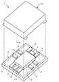
図1は、本発明の第1の実施形態に係る電子部品装置を説明するための分解斜視図であり、図2は、該電子部品装置の要部を示す模式的平面図である。 FIG. 1 is an exploded perspective view for explaining an electronic component device according to a first embodiment of the present invention, and FIG. 2 is a schematic plan view showing a main part of the electronic component device.
図1に示すように、本実施形態の電子部品装置1は、矩形板状の基板2を有する。基板2上には、比較的大きな電子部品3と、複数のチップ型電子部品4〜13が表面実装されている。
As shown in FIG. 1, the
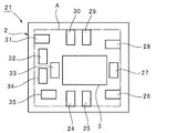
ここでは、チップ型電子部品4〜13が実装されている領域の外周縁が一点鎖線Aで示されている。ここでは、電子部品3は、例えばICや弾性表面波装置などの比較的大きな実装面積を有する電子部品である。これに対して、チップ型電子部品4〜13は、チップ型積層コンデンサなどの比較的小型の電子部品であり、本実施形態では、チップ型電子部品4〜13は0.5mm2以下の矩形の実装面積を有する。ここで、実装面積とは、チップ型電子部品が基板2上に実装された際に、基板2上に占める領域をいうものとする。言い換えれば、実装された電子部品を下方の基板2上に投影した場合該投影された領域が実装面である。チップ型電子部品4〜13の実装面は、本実施形態では、長方形とされている。もっとも、長方形のコーナー部分が丸められた略長方形であってもよい。
Here, the outer peripheral edge of the area where the chip-type
複数のチップ型電子部品4〜13は様々な機能及び寸法を有するチップ型電子部品であるが、これらのうち、チップ型電子部品4〜6,8〜13は、実装領域の外周縁Aに接するように実装されている。ここで、実装領域とは、複数のチップ型電子部品4〜13が基板2上に実装される領域をいうものとする。本実施形態では、実装領域は、複数のチップ型電子部品4〜13が実装されている領域であって、かつ対向し合う一対の第1の辺と、対向し合う他の一対の第2の辺とを有する矩形の領域とされている。該矩形の領域内に、複数のチップ型電子部品4〜13が実装されている。
The plurality of chip-type
チップ型電子部品4を例にとると、チップ型電子部品4の実装面は長方形の形状を有し、その一方の短辺が実装領域の外周縁Aに接するように、長辺が上記短辺が接している外周縁部分と略直交する方向に延びるようにチップ型電子部品4が配置されている。
Taking the chip-type
このような長方形の実装面を有するチップ型電子部品4に、基板2の面方向に沿う外力が加わった場合、外力が大きいとチップ型電子部品4が基板2から外れるおそれがある。ところが、実装面が長方形の場合には、該実装面である長方形の長辺方向に外力が加わった場合には、短辺方向に沿う外力が加わった場合に比べて、チップ型電子部品4は基板2から外れ難い。言い換えれば、短辺方向に沿う実装強度に比べて、長辺方向に沿う実装強度は相対的に高い。
When an external force along the surface direction of the
チップ型電子部品4だけでなく、チップ型電子部品5,6、8〜13も同様に、長方形の実装面のうち一方の短辺が外周縁Aに接するように、かつ該短辺が接している外周縁部分に上記長方形の長辺が略直交する方向となるように、基板2上に実装されている。
Similarly, not only the chip-type
他方、基板2上には、図1に上方に示すケース材14が搭載される。ケース材14は、下方に開いた開口14aを有する。本実施形態では、ケース材14は金属からなるが、金属以外のセラミックスなどによりケース材14が構成されてもよい。ケース材14の開口14aの周縁部が基板2の上面に接合される。この接合に際しては、はんだや絶縁性接着剤などが用いられる。
On the other hand, a
ところで、前述したように、電子部品装置では小型化が進んでおり、上記実装領域内には多数のチップ型電子部品4〜13が高密度に実装されている。しかも、実装領域の外側近傍において、上記ケース材14の下方の開口周縁部が基板2に接合される。この場合、ケース材14の搭載位置が若干ずれた場合、ケース材14の開口周縁部がチップ型電子部品4〜6,8〜13に接触するおそれがある。
By the way, as described above, the electronic component device has been reduced in size, and a large number of chip-type
前述したように、従来の複合電子部品101では、このような接触が生じた場合、衝撃によりチップ型電子部品107〜109が基板102から離脱するおそれがあった。
As described above, in the conventional composite
これに対して、本実施形態の電子部品装置1では、外周縁Aに接触するように実装されているチップ型電子部品4〜6,8〜13は、上記実装面である長方形の一方の短辺が外周縁Aに接するように実装されている。従って、ケース材14の開口周縁部が接触し、チップ型電子部品4〜6,8〜13のいずれかに衝撃が加わったとしても、チップ型電子部品4〜6,8〜13には上記長方形のその長辺方向に加わることとなる。従ってチップ型電子部品4〜6,8〜13は、基板2上から脱離し難い。よって、実装不良が生じ難い電子部品装置1を提供することができる。
On the other hand, in the
なお、本実施形態では、外周縁Aに接触しないように配置されている第2のチップ型電子部品7がさらに備えられているが、チップ型電子部品7は必ずしも設けられずともよい。また、外周縁Aに接触しないように配置される第2のチップ型電子部品は複数であってもよい。 In the present embodiment, the second chip type electronic component 7 arranged so as not to contact the outer peripheral edge A is further provided, but the chip type electronic component 7 may not necessarily be provided. In addition, a plurality of second chip-type electronic components may be arranged so as not to contact the outer peripheral edge A.
さらに、大型の電子部品3が実装領域内に実装されていたが、大型の電子部品3は実装領域内に実装されておらずともよい。
Furthermore, although the large
チップ型電子部品4〜6,8〜13の基板2上に接合される態様についても特に限定されず、例えば長方形の実装面において、長辺方向と平行な方向において隔てられた複数の接合部分によりチップ型電子部品4〜6,8〜13が基板2上の電極ランド(図示せず)に接合されてもよく、1箇所の接合部分により基板2上の電極ランドに接合されていてもよい。いずれにしても、略長方形の実装面を有するチップ型電子部品は、通常、その長方形の長辺方向に力が加わった場合、短辺方向に力が加わった場合に比べて外れ難いように実装されている。従って、チップ型電子部品4〜6,8〜13の具体的な実装構造の如何に関わらず、上記のように、長辺方向に力が加わった場合には、短辺方向に沿う力が加わった場合に比べて基板2から脱離し難い。
The aspect of the chip-type
図3及び図4は、本発明の電子部品装置の変形例を示す各模式的平面図である。 3 and 4 are each a schematic plan view showing a modification of the electronic component device of the present invention.
図3に示す変形例の電子部品装置21では、基板2上に、実装面積が0.5mm2よりも大きな大型の電子部品3と、実装面積が0.5mm2以下である長方形の実装面積を有する複数のチップ型電子部品24〜35とが表面実装されている。これらのうち、チップ型電子部品24〜26,28〜31が、実装領域の外周縁Aに長方形の実装面の一方の短辺が接するように実装されているチップ型電子部品である。他方、チップ型電子部品27,32〜35は、実装領域内において実装されている第2のチップ型電子部品である。
In the
また、図4に示す変形例の電子部品装置41では、基板2上において、実装面積が0.5mm2よりも大きな大型の電子部品3と、実装面積が0.5mm2以下の略長方形のチップ型電子部品44〜54が実装されている。ここでは、実装領域Aに外周縁が接するように実装されている電子部品は、チップ型電子部品44,45,47,48,50,51,53,54である。そして、チップ型電子部品45,46,49,52は、実装領域内において表面実装されている。
Further, in the
図4において、電子部品3は、比較的大きい電子部品であり、その実装面の面積は0.5mm2よりも大きい。該電子部品3の実装面の長辺は外周縁Aに接触するように配置されている。しかしながら、電子部品3の実装面を構成している長方形の短辺方向に応力が加わったとしても、実装面積が大きいため、電子部品3は基板2から脱離し難い。
In FIG. 4, the
図3及び図4に示した電子部品装置21,41に示すように、本発明においては、基板上に複数のチップ型電子部品が搭載される態様は様々に変形することができ、いずれの場合においても、長方形の実装面を有するチップ型電子部品であって、実装領域の外周縁Aに接するように実装されるチップ型電子部品は、その実装面を構成している一方の短辺が外周縁Aに接触し、かつ長辺が該短辺が接触している外周縁部分に直交する方向に延びるように実装されておればよい。
As shown in the
このことを明らかにするために、本発明に含まれない電子部品装置の例を図5(a)及び(b)にそれぞれ示す。 In order to clarify this, examples of electronic component devices not included in the present invention are shown in FIGS. 5 (a) and 5 (b), respectively.
図5(a)に示す電子部品装置121では、実装領域の外周縁が一点鎖線Aで示されている。ここでは、基板122上に、実装面積が0.5mm2よりも大きな大型の電子部品123と、実装面積が0.5mm2以下の長方形の複数のチップ型電子部品124〜134とが実装されている。しかしながら、チップ型電子部品127は、実装面が長方形のチップ型電子部品であるが、その実装面の長辺が実装領域の外周縁Aに接触するように、かつ短辺が長辺が接触している外周縁部分に直交する方向に延びるように実装されている。従って、ケース材を搭載した際の位置ずれにより、チップ型電子部品127にケース材の一部が接触した場合には、その応力は上記短辺方向に伝わることとなる。従って、チップ型電子部品127の基板2からの脱離が生じ易い。
In the
また、図5(b)に示すチップ型電子部品141では、基板142上に、実装面積が0.5mm2よりも大きな大型の電子部品143と、実装面積が0.5mm2以下の長方形である複数のチップ型電子部品144〜154とが実装されている。チップ型電子部品154は、その実装面である長方形の長辺方向だけでなく、短辺も外周縁Aに接触するように配置されている。従って、チップ型電子部品154は、ケース材を搭載する際にケース材の一部が接触すると、該実装面の短辺方向に応力が加わり易く、基板2から脱離し易い。
5B is a large
1…電子部品装置
2…基板
3…電子部品
4〜13…チップ型電子部品
14…ケース材
14a…開口
21…電子部品装置
23…電子部品
24〜35…チップ型電子部品
41…電子部品装置
43…電子部品
44〜54…チップ型電子部品
DESCRIPTION OF
Claims (2)
前記基板の一方主面の実装領域上に表面実装された複数のチップ型電子部品とを備え、
前記複数のチップ型電子部品のうち、前記実装領域の外周縁に接するように実装されており、かつ0.5mm2以下の略長方形の実装面を有している全てのチップ型電子部品が、前記略長方形の一方の短辺が当該電子部品が接している前記実装領域の外周縁に沿うように、かつ該長方形の長辺は前記外周縁に沿わないように前記外周縁と略直交する方向に延びるように配置されており、前記実装領域に搭載されており、該実装領域の外周縁に接しないように配置された少なくとも1個の第2のチップ型電子部品をさらに備えることを特徴とする、電子部品装置。 On the other hand, a substrate having a mounting area on the main surface;
A plurality of chip-type electronic components surface-mounted on a mounting region of one main surface of the substrate;
Among the plurality of chip-type electronic components, all the chip-type electronic components mounted so as to be in contact with the outer peripheral edge of the mounting region and having a substantially rectangular mounting surface of 0.5 mm 2 or less, A direction substantially perpendicular to the outer peripheral edge so that one short side of the substantially rectangular shape is along the outer peripheral edge of the mounting region in contact with the electronic component, and the long side of the rectangular is not along the outer peripheral edge. is arranged to extend, is mounted on the mounting region, further comprising wherein Rukoto at least one of the second chip-type electronic component disposed so as not to contact the outer peripheral edge of the mounting area An electronic component device.
Priority Applications (1)
| Application Number | Priority Date | Filing Date | Title |
|---|---|---|---|
| JP2004350055A JP4720162B2 (en) | 2004-12-02 | 2004-12-02 | Electronic component equipment |
Applications Claiming Priority (1)
| Application Number | Priority Date | Filing Date | Title |
|---|---|---|---|
| JP2004350055A JP4720162B2 (en) | 2004-12-02 | 2004-12-02 | Electronic component equipment |
Publications (2)
| Publication Number | Publication Date |
|---|---|
| JP2006165049A JP2006165049A (en) | 2006-06-22 |
| JP4720162B2 true JP4720162B2 (en) | 2011-07-13 |
Family
ID=36666746
Family Applications (1)
| Application Number | Title | Priority Date | Filing Date |
|---|---|---|---|
| JP2004350055A Expired - Fee Related JP4720162B2 (en) | 2004-12-02 | 2004-12-02 | Electronic component equipment |
Country Status (1)
| Country | Link |
|---|---|
| JP (1) | JP4720162B2 (en) |
Citations (4)
| Publication number | Priority date | Publication date | Assignee | Title |
|---|---|---|---|---|
| JP2000195996A (en) * | 1998-12-24 | 2000-07-14 | Kyocera Corp | Electronic circuit module |
| JP2001068615A (en) * | 1999-08-26 | 2001-03-16 | Tdk Corp | Power amplifier module |
| WO2004001963A1 (en) * | 2002-06-25 | 2003-12-31 | Epcos Ag | Electronic component comprising a multilayer substrate and corresponding method of production |
| JP2004071977A (en) * | 2002-08-08 | 2004-03-04 | Mitsubishi Electric Corp | Semiconductor device |
-
2004
- 2004-12-02 JP JP2004350055A patent/JP4720162B2/en not_active Expired - Fee Related
Patent Citations (4)
| Publication number | Priority date | Publication date | Assignee | Title |
|---|---|---|---|---|
| JP2000195996A (en) * | 1998-12-24 | 2000-07-14 | Kyocera Corp | Electronic circuit module |
| JP2001068615A (en) * | 1999-08-26 | 2001-03-16 | Tdk Corp | Power amplifier module |
| WO2004001963A1 (en) * | 2002-06-25 | 2003-12-31 | Epcos Ag | Electronic component comprising a multilayer substrate and corresponding method of production |
| JP2004071977A (en) * | 2002-08-08 | 2004-03-04 | Mitsubishi Electric Corp | Semiconductor device |
Also Published As
| Publication number | Publication date |
|---|---|
| JP2006165049A (en) | 2006-06-22 |
Similar Documents
| Publication | Publication Date | Title |
|---|---|---|
| US10531559B2 (en) | Electronic device | |
| JP2006210852A (en) | Circuit board with surface-mounting circuit component, and its manufacture | |
| JP2006074736A (en) | Piezoelectric oscillator and method of manufacturing the same | |
| JP2010278133A (en) | Circuit board | |
| JP4527035B2 (en) | Shield structure | |
| JP5962746B2 (en) | Piezoelectric transformer device | |
| JP2008113894A (en) | Semiconductor device and electronic equipment | |
| JP4720162B2 (en) | Electronic component equipment | |
| JP2007243536A (en) | Piezoelectric device and its manufacturing method | |
| JP2007294649A (en) | Surface-mounting electronic device | |
| JP4086657B2 (en) | Multilayer semiconductor device | |
| JP6323622B2 (en) | Component mounting board | |
| JPH09186042A (en) | Laminated electronic component | |
| JP2009164560A (en) | Mounting structure, electrooptical device, and electronic apparatus | |
| JP7182712B2 (en) | Electronic component storage packages, electronic devices, and electronic modules | |
| JP2008112832A (en) | High-frequency unit, and manufacturing method of high-frequency unit | |
| JP2001326428A (en) | Printed circuit board | |
| JP6236367B2 (en) | Sensor module and method of manufacturing sensor module | |
| JP5776373B2 (en) | Electronic equipment | |
| JP2006229447A (en) | Television reception tuner | |
| JP2007189580A (en) | Piezoelectric device and housing container therefor | |
| JP4636827B2 (en) | Circuit module | |
| JP5437670B2 (en) | Electronic circuit unit | |
| JP3110725U (en) | Semiconductor device | |
| JP2010010212A (en) | Printed circuit board, electronic instrument and semiconductor package |
Legal Events
| Date | Code | Title | Description |
|---|---|---|---|
| A621 | Written request for application examination |
Free format text: JAPANESE INTERMEDIATE CODE: A621 Effective date: 20070926 |
|
| A977 | Report on retrieval |
Free format text: JAPANESE INTERMEDIATE CODE: A971007 Effective date: 20080229 |
|
| A131 | Notification of reasons for refusal |
Free format text: JAPANESE INTERMEDIATE CODE: A131 Effective date: 20100629 |
|
| A521 | Written amendment |
Free format text: JAPANESE INTERMEDIATE CODE: A523 Effective date: 20100825 |
|
| A131 | Notification of reasons for refusal |
Free format text: JAPANESE INTERMEDIATE CODE: A131 Effective date: 20101221 |
|
| A521 | Written amendment |
Free format text: JAPANESE INTERMEDIATE CODE: A523 Effective date: 20110215 |
|
| A01 | Written decision to grant a patent or to grant a registration (utility model) |
Free format text: JAPANESE INTERMEDIATE CODE: A01 Effective date: 20110308 |
|
| A61 | First payment of annual fees (during grant procedure) |
Free format text: JAPANESE INTERMEDIATE CODE: A61 Effective date: 20110321 |
|
| FPAY | Renewal fee payment (event date is renewal date of database) |
Free format text: PAYMENT UNTIL: 20140415 Year of fee payment: 3 |
|
| R150 | Certificate of patent or registration of utility model |
Free format text: JAPANESE INTERMEDIATE CODE: R150 |
|
| LAPS | Cancellation because of no payment of annual fees |