JP4704529B2 - SRAM device and manufacturing method thereof - Google Patents
SRAM device and manufacturing method thereof Download PDFInfo
- Publication number
- JP4704529B2 JP4704529B2 JP25484898A JP25484898A JP4704529B2 JP 4704529 B2 JP4704529 B2 JP 4704529B2 JP 25484898 A JP25484898 A JP 25484898A JP 25484898 A JP25484898 A JP 25484898A JP 4704529 B2 JP4704529 B2 JP 4704529B2
- Authority
- JP
- Japan
- Prior art keywords
- interlayer insulating
- insulating film
- forming
- conductive film
- transistors
- Prior art date
- Legal status (The legal status is an assumption and is not a legal conclusion. Google has not performed a legal analysis and makes no representation as to the accuracy of the status listed.)
- Expired - Fee Related
Links
Images


Classifications
-
- H—ELECTRICITY
- H10—SEMICONDUCTOR DEVICES; ELECTRIC SOLID-STATE DEVICES NOT OTHERWISE PROVIDED FOR
- H10B—ELECTRONIC MEMORY DEVICES
- H10B10/00—Static random access memory [SRAM] devices
-
- H—ELECTRICITY
- H10—SEMICONDUCTOR DEVICES; ELECTRIC SOLID-STATE DEVICES NOT OTHERWISE PROVIDED FOR
- H10B—ELECTRONIC MEMORY DEVICES
- H10B10/00—Static random access memory [SRAM] devices
- H10B10/12—Static random access memory [SRAM] devices comprising a MOSFET load element
-
- H—ELECTRICITY
- H10—SEMICONDUCTOR DEVICES; ELECTRIC SOLID-STATE DEVICES NOT OTHERWISE PROVIDED FOR
- H10B—ELECTRONIC MEMORY DEVICES
- H10B10/00—Static random access memory [SRAM] devices
- H10B10/12—Static random access memory [SRAM] devices comprising a MOSFET load element
- H10B10/125—Static random access memory [SRAM] devices comprising a MOSFET load element the MOSFET being a thin film transistor [TFT]
-
- H—ELECTRICITY
- H10—SEMICONDUCTOR DEVICES; ELECTRIC SOLID-STATE DEVICES NOT OTHERWISE PROVIDED FOR
- H10B—ELECTRONIC MEMORY DEVICES
- H10B99/00—Subject matter not provided for in other groups of this subclass
Landscapes
- Semiconductor Memories (AREA)
Description
【0001】
【発明の属する技術分野】
本発明は、SRAM(Static Random Access Memory)装置およびその製造方法に関する。
【0002】
【従来の技術】
一般に、SRAMはDRAMに比べ集積度は劣るが、高速に動作するため中型または小型コンピュータの分野で広く使われている。SRAMのメモリセルは通常2個の伝送トランジスタと2個の駆動トランジスタ、そして2個の負荷素子から構成されるフリップフロップ回路から構成されている。記憶情報はフリップフロップの入力、出力端子間の電圧差、すなわちセルのNODEに蓄積された電荷として保存される。この電荷は電源Vccから負荷素子であるPMOS(P-Metal-Oxide-Semiconductor)トランジスタや負荷抵抗を通じて常に補充されているので、SRAMではDRAMのようにリフレッシュ機能が要求されない。
SRAMの高速動作特性を維持し向上させるためにはチップの構造、メモリセルを構成する回路の構成または配線構成を最適化する必要がある。特に配線をどのように配列するかによって配線抵抗と配線間の寄生容量が決定する。
【0003】
図1は、従来のSRAMにおいてワードラインに発生する寄生容量をPMOSTFTを使用するCMOS型SRAMチップから隣接した二つのSRAMセルをワードライン方向を追って切断した断面図である。
半導体基板10上に形成された素子分離膜12により活性領域と非活性領域が区別されており、ゲート絶縁膜13を介在し伝送トランジスタのゲート14と駆動トランジスタのゲート16が形成されている。ゲート14、16上に第1層間絶縁膜18とワードライン20が順序通り積層されている。ワードライン20は第1層間絶縁膜18内に形成されたコンタクトホールを通じ伝送トランジスタのゲート14と連結されている。ワードライン20上に第2層間絶縁膜22およびPMOS TFTのゲート絶縁膜24が順序通り積層されている。ゲート絶縁膜24の上部にはPMOS TFTのソース領域と一体で形成される電源線26がワードライン20と平行に形成されている。電源線26の上部に第3層間絶縁膜28が積層されており、第3層間絶縁膜28の上部にワードライン20と垂直になるように配置された複数本のビットライン30が形成されている。
【0004】
【発明が解決しようとする課題】
ところが、図1に示されているものと同じ構造のSRAMセルにおいてはワードライン20と電源線26間C1、ワードライン20と基板10間C2、ワードライン20と駆動トランジスタのゲート電極16間C3に寄生容量が発生するようになる。
【0005】
各ワードラインは横方向に隣接した全てのセルに共通で連結されるという点を考慮する時、ワードライン20と電源線26の全面に渡り形成される寄生容量C1およびワードライン20と基板10間、そしてワードライン20と駆動トランジスタのゲート電極16間で発生する寄生容量C2、C3はワードラインの抵抗係数(以下、RC)遅延を起こすに十分に大きな値になる。また、従方向に隣接した全てのセルごとにそれぞれ2本のワードラインが配置されるということを考慮する時、ワードラインの寄生容量はチップの動作速度を顕著に減少させチップ性能を劣化させる。
【0006】
本発明の目的は、ワードラインに発生する寄生容量を最小化することができるSRAM装置を提供することにある。
本発明の別の目的は、SRAM装置を製造することに適合する製造方法を提供することにある。
【0007】
【課題を解決するための手段】
本発明のSRAM装置によると、SRAMを構成するメモリセルは2個の伝送トランジスタ、2個の駆動トランジスタ、2本の電源線および2本のワードラインから構成される。2個の伝送トランジスタと2個の駆動トランジスタは半導体基板上に形成され第1導電膜からなる。2本の電源線は4個のトランジスタ上に4個のトランジスタとそれぞれ絶縁されて形成され第2導電膜からなる。2本のワードラインは2本の電源線上に2本の電源線とそれぞれ絶縁されて形成され、2個の伝送トランジスタのゲートとそれぞれ接続され、第3導電膜からなる。
【0008】
本発明において、2本の電源線と2本のワードラインはそれぞれ長手方向に平行に形成されている。
メモリセルは2個の負荷素子をさらに備えている。2個の負荷素子はPMOS型薄膜トランジスタであり、2本の電源線はそれぞれ2個のPMOS型薄膜トランジスタの活性領域と連結されて形成される。また、2個の負荷素子は2個の高抵抗の多結晶シリコン負荷であり、2本の電源線はそれぞれ2個の高抵抗の多結晶シリコン負荷と連結され形成される場合もある。
【0009】
また、メモリセルはワードラインを構成する第3導電膜と同一な導電膜からなり、半導体基板上の活性領域と接続する接地線をさらに備えている。
2本のワードラインと絶縁され2本のワードラインと垂直に形成される2本のビットラインをさらに備えることができ、2本のビットラインはそれぞれ半導体基板、電源線およびワードラインをそれぞれ絶縁させるために形成された第1および第2層間絶縁膜内に形成されたコンタクトプラグとワードラインとビットラインを絶縁させるため形成された第3層間絶縁膜内に形成され、コンタクトプラグを露出させるコンタクトホール内に蒸着された第4導電膜パターンからなることが望ましい。
【0010】
また、SRAMを構成するメモリセルは2個の伝送トランジスタ、2個の駆動トランジスタ、電源線およびワードラインから構成されている。2個の伝送トランジスタと2個の駆動トランジスタは半導体基板上に形成され第1導電膜からなる。電源線は4個のトランジスタ上に4個のトランジスタとそれぞれ絶縁されて形成され第2導電膜からる。ワードラインは電源線上に電源線とそれぞれ絶縁されて形成され、2個の伝送トランジスタのゲートとそれぞれ接続され、第3導電膜からる。
【0011】
本発明のSRAM装置の製造方法によれば、まず半導体基板上に第1導電膜パターンを形成する。次に第1導電膜パターンが形成された結果物全面に不純物を注入し第1導電膜パターンをそれぞれゲート電極として備える2個の伝送トランジスタと2個の駆動トランジスタを形成する。続いて、4個のトランジスタが形成された結果物上に第1層間絶縁膜を形成した後、第1層間絶縁膜上に第2導電膜パターンからなる2本の電源線を形成する。2本の電源線上に第2層間絶縁膜を形成した後、第2層間絶縁膜および第1層間絶縁膜を蝕刻し2個の伝送トランジスタのゲートをそれぞれ露出させる2個のコンタクトホールを形成する。最後に2個のコンタクトホールを埋め立てる第3導電膜パターンを形成し2個の伝送トランジスタのゲートと接続する2本のワードラインを形成する。
【0012】
本発明において、電源線を構成する第2導電膜パターンとワードラインを構成する第3導電膜パターンはそれぞれ長さ方向に平行に形成される。
第1層間絶縁膜を形成する段階以後は、次のような段階を進行することが望ましい。すなわち、第1層間絶縁膜上に2個の薄膜トランジスタのゲート電極2個を形成した後、2個の薄膜トランジスタのゲート電極が形成された結果物上にゲート絶縁膜を形成する。そして、ゲート絶縁膜上に第2導電膜パターンを形成した後、第2導電膜パターンの中薄膜トランジスタのチャンネルとして形成される領域を除いた領域に不純物を注入し2個の薄膜トランジスタからなる負荷素子と2本の電源線を形成する。
【0013】
2本の電源線を形成する他の方法によれば、第1層間絶縁膜上に多結晶シリコンからなる第2導電膜パターンを形成した後、第2導電膜パターンの高抵抗負荷として形成される領域を除いた領域に不純物を注入し2個の高抵抗負荷および2本の電源線を形成する段階を含むことが望ましい。
【0014】
そして、上記の製造方法において第2層間絶縁膜を形成する段階以後は、次のような段階を進行することが望ましい。まず、第2層間絶縁膜を形成した後、第2層間絶縁膜を平坦化した後、ダマシン(damascene)工程で平坦化された第2層間絶縁膜を部分的に蝕刻し、2本のワードラインが形成される2個のダマシン領域を形成する。そして、ダマシン領域が形成された第2層間絶縁膜および第1層間絶縁膜を蝕刻し2個の伝送トランジスタのゲートをそれぞれ露出させる2個のコンタクトホールを形成する。次に2個のコンタクトホールおよび2個のダマシン領域を埋め立てる第3導電膜を形成した後、第2層間絶縁膜表面が露出されるまで第3導電膜を平坦化し、2個の伝送トランジスタのゲートと接続する2本のワードラインを形成する。
【0015】
また、上記の製造方法において第2層間絶縁膜を形成する段階以後は、次のような段階を進行する場合もある。まず第2層間絶縁膜を平坦化した後、ダマシン工程で平坦化した第2層間絶縁膜を部分的に蝕刻しワードラインが形成される2個のダマシン領域および接地線が形成されるダマシン領域を形成する。次に、ダマシン領域が形成された第2層間絶縁膜および第1層間絶縁膜を蝕刻し、2個の伝送トランジスタのゲートをそれぞれ露出させる2個のコンタクトホールおよび2個の駆動トランジスタの活性領域を露出させる2個のコンタクトホールを形成する。引続き、コンタクトホールおよびダマシン領域を埋め立てる第3導電膜を形成した後、第2層間絶縁膜表面が露出するまで第3導電膜を平坦化し、2個の伝送トランジスタのゲートと接続する2本のワードラインおよび2個の駆動トランジスタの活性領域と接続する接地線を形成する。
【0016】
本発明はまた、2本のワードラインを形成する段階以後は、次のような段階をさらに遂行することが望ましい。まず、第3層間絶縁膜を形成した後、第3、第2および第1層間絶縁膜を蝕刻し、半導体基板の活性領域を露出させるコンタクトホールを形成する。次にコンタクトホールを埋め立て第3層間絶縁膜上に形成され、2本のワードラインとそれぞれ垂直な第4導電膜パターンを形成し2本のビットラインを形成する。
【0017】
また、第2層間絶縁膜を形成する段階以後の工程は、次の通り進行する場合もある。まず第2層間絶縁膜を平坦化した後、ワードラインが形成されるダマシン領域が形成された第2層間絶縁膜および第1層間絶縁膜を蝕刻し、2個の伝送トランジスタのゲートをそれぞれ露出させる2個のコンタクトホールおよび半導体基板の活性領域を露出させる2個のコンタクトホールを形成する。続いて、コンタクトホールおよび2個のダマシン領域を埋め立てる第3導電膜を形成した後、第2層間絶縁膜表面が露出するまで第3導電膜を平坦化し、2個の伝送トランジスタのゲートと接続する2本のワードラインおよび基板上の活性領域と接続するコンタクトプラグを形成する。次に、2本のワードラインおよび2個のコンタクトプラグが形成された結果物全面に第3層間絶縁膜を形成する。続いて、第3層間絶縁膜を蝕刻し、2個のコンタクトプラグを露出させる2個のコンタクトホールを形成した後、2個のコンタクトプラグを露出させる2個のコンタクトホールを埋め立てる2個の第4導電膜パターンを形成し、2本のビットラインを形成する。
【0018】
また、本発明のSRAM装置の製造方法によれば、まず半導体基板上に第1導電膜パターンを形成する。次に第1導電膜パターンが形成された結果物全面に不純物を注入し第1導電膜パターンをそれぞれゲート電極として備える2個の伝送トランジスタと2個の駆動トランジスタを形成する。続いて、4個のトランジスタが形成された結果物上に第1層間絶縁膜を形成した後、第1層間絶縁膜上に第2導電膜パターンからなる電源線を形成する。電源線上に第2層間絶縁膜を形成した後、第2層間絶縁膜および第1層間絶縁膜を蝕刻し2個の伝送トラジスタのゲートをそれぞれ露出させる2個のコンタクトホールを形成する。最後に2個のコンタクトホールを埋め立てる第3導電膜パターンを形成し2個の伝送トランジスタのゲートと接続するワードラインを形成する。
本発明のSRAM装置によると、ワードラインの寄生容量が減少するためにSRAM装置の動作時ワードラインで発生するRC遅延問題を解決でき、SRAM装置の動作特性を向上させることができる。
【0019】
【発明の実施の形態】
以下添付した図面を参照して本発明の望ましい実施例を説明することによって本発明を詳細に説明する。しかし本発明は以下に開示される実施例に限らず相異なる多様な形態で具現されることであり、単に本実施例は本発明の開示が完全なるようにし、通常の知識を有する者に発明の範疇を完全に知らせるために提供されることである。添付された図面における多様な膜と領域の厚さは明瞭性のため強調された。また、ある一膜が他の膜または基板上に存在することと指称される時、他の膜または基板の真上にあることもあり、層間膜が存在する場合もある。図面で同一参照符号は同一部材を示す。
【0020】
<SRAMセル>
(第1実施例)
本発明の第1実施例にともなうSRAMチップにおいてワードライン方向を追って隣接した二つのセルを切断した断面図が図2に示されている。第1実施例はPMOS型TFTを負荷素子として使用するSRAMセルを具現する。
図2を参照すれば、素子分離膜102により半導体基板100が活性領域と非活性領域に区別されており、同一導電膜からなる伝送トランジスタのゲート104と駆動トランジスタのゲート106が半導体基板100上に形成されている。ゲート104、106上に第1層間絶縁膜107とPMOS TFTのゲート絶縁膜111が順序通り積層されている。ゲート絶縁膜111上面にPMOS TFTの活性領域および電源線として使われる導電膜パターン114が形成されており、導電膜パターン114が形成された結果物全面に第2層間絶縁膜115が積層されている。第2層間絶縁膜115、ゲート絶縁膜111および第1層間絶縁膜107を貫通し伝送トランジスタのゲート104を露出させるコンタクトホールを通じ伝送トランジスタのゲート104と接続するワードライン122が第2層間絶縁膜115上に形成されている。最後に第3層間絶縁膜125によりワードライン122と絶縁され、ワードライン122と垂直に配列された複数本のビットライン128が形成されている。
【0021】
図2に示されているように本発明の第1実施例にともなうPMOS TFTを負荷抵抗として使用するCMOSSRAMではワードライン122が電源線114により下部導電領域、例えばゲートから遮られるシールディング効果があるためワードライン122と半導体基板100間の寄生容量(図1のC2参考)およびワードライン122と駆動トランジスタのゲート電極106間の寄生容量(図1のC3)が発生しない。すなわち、従来のSRAMセルに比べワードライン122の寄生容量が減少するので動作速度もさらに速くなり高速動作特性を要求するSRAMの性能を向上させることができる。
【0022】
また、電源線114とワードライン122間の寄生容量C1も電源線114からワードライン122を絶縁させる第2層間絶縁膜115の厚さを増やすことによって従来の寄生容量(図1のC1参考)より効果的に減少させることができる。その理由は段差に多くの影響を受けるPMOS TFTが既に電源線114下に形成されているため第2層間絶縁膜115の厚さを増やしてもワードライン122とビットライン128のみ段差による影響を受けるためである。
【0023】
ただし、本発明の構造にしたがう場合従来のSRAMにはなかったワードライン122とビットライン128間の寄生容量C4が形成されることがあるが、このような寄生容量C4は第3層間絶縁膜125の厚さを増やすことによって十分に減らすことができる。第3層間絶縁膜125の厚さを増やす場合段差が増えることはあるが、段差による影響を受けることはビットライン128のみである。そして第3層間絶縁膜125の増加により発生する段差問題は半導体基板100上の活性領域とビットライン128を接触させるためのコンタクトホールをコンタクトプラグ(図11Bの120P参考)を用いて形成すれば減らすことができる。
【0024】
反面、図1に示されている従来のSRAM構造においては寄生容量C2およびC3を減らすため第1層間絶縁膜18および第2層間絶縁膜22の厚さを増やす場合ワードライン20形成時段差が増えてワードライン20上に形成されるPMOS TFTの活性領域用導電膜形成時には段差がさらに加重される。したがって寄生容量を減らすため層間絶縁膜の厚さを増やすことには限界が伴うようになる。
【0025】
(第2実施例)
図3には本発明の第2実施例によるSRAMチップからワードライン方向を追って隣接した二つのセルを切断した断面図が示されている。第2実施例が第1実施例と異なる点は負荷素子としてPMOS TFTを使用することでなく高抵抗の多結晶シリコンからなる高抵抗負荷を使用するということである。
それゆえにその他構成要素および構造は図2とほとんど同一であり、ただしPMOS TFTゲート(図示せず)および絶縁膜111が要らなく、第1層間絶縁膜107上にPMOS TFT活性領域と連結された電源線114が形成される代わりに高抵抗の負荷と連結された電源線114Rが形成されるという点に差がある。
【0026】
第2実施例においても第1実施例と同じく、ワードライン122が電源線114R上に形成されるためワードライン122と駆動トランジスタのゲート106およびワードライン122と基板100間に寄生容量が発生しないのでSRAMセルの動作速度を向上させることができる。
図面には示しなかったが本発明にともなう構造を負荷素子としてPMOSトランジスタを使用する完全CMOS型SRAMに適用できることはもちろんである。
【0027】
<SRAMセルの製造方法>
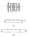
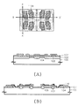
図4ないし図13には本発明の第1実施例によるSRAMセルを製造するための工程に必要であるマスクパターンのレイアウト図を示した。各レイアウト図において、斜線影を付けた部分はそれぞれフォトマスク上に形成されたマスクパターンを意味する。説明の便宜のため隣接した4個のSRAMセルを基準としてレイアウト図を示した。また、図4Aないし図13Aおよび図4Bないし図13Bはそれぞれ、前記図4ないし図13のAA’線およびBB’線を切って見た断面図であり、各レイアウト図に描いたマスクパターンを用いてSRAMセルを製造する工程の中間段階構造物の断面図を示す。
【0028】
図4、図4Aおよび図4Bは活性領域を限定するマスクパターン102Mを用いて半導体基板100上にフィールド酸化膜102を形成する段階を示す。フィールド酸化膜102は通常の方式、例えば局部的酸化方式(LOCOS)によって形成する。この時、一つのメモリセルのフィールド酸化膜102は隣接するメモリセルのフィールド酸化膜と鏡上対称である。
図5、図5Aおよび図5Bは伝送トランジスタのゲートと駆動トランジスタのゲートを限定するマスクパターン104Mおよび106Mを用いて、伝送トランジスタおよび駆動トランジスタを形成する段階を示す。
【0029】
フィールド酸化膜102が形成された半導体基板100全面に、ゲート絶縁膜(図示せず)を形成した次に、ゲート絶縁膜上に導電物質、例えば多結晶シリコンをデポジットしたりあるいは多結晶シリコンとシリサイドを積層し導電層を形成する。続いて、マスクパターン104Mおよび106Mを用いた写真蝕刻工程で導電層をパターニングする。その結果一つのメモリセルには2個の伝送トランジスタのゲート104および2個の駆動トランジスタのゲート106がそれぞれ形成される。
【0030】
次に、トランジスタのゲート104、106が形成された結果物全面に不純物、例えば燐または砒素をイオン注入し伝送トランジスタおよび駆動トランジスタの活性領域すなわち、ソースおよびドレーン領域をそれぞれ形成することによって各トランジスタを完成する。
図6、図6Aおよび図6Bはセルをラッチ形態で連結するためのセルノード用コンタクトホールを限定するマスクパターン108Mを用いてコンタクトホール108を形成する段階を示す。
【0031】
まず伝送トランジスタおよび駆動トランジスタが形成された結果物全面に第1層間絶縁膜107を形成する。次に、図6に示されたようなマスクパターン108Mを用いた写真蝕刻工程で第1層間絶縁膜107を部分的に取り除くことによって、駆動トランジスタのゲート106の一部および伝送トランジスタのソース領域を露出させるセルノード用コンタクトホール108を形成する。
図7、図7Aおよび図7BはPMOS TFTのゲートを限定するマスクパターン110Mを用いてPMOS TFTのゲート110を形成する段階を示す。
【0032】
セルノード用コンタクトホール108が形成された結果物全面に導電膜を蒸着した後、図7に示されているマスクパターン110Mを用いた写真蝕刻工程で導電膜をパターニングしPMOS TFTのゲート110を形成する。各メモリセル別に2個のPMOS TFTのゲート110が形成される。PMOS TFTのゲート110はセルノード用コンタクトホール108を通じ駆動トランジスタのゲート106の一部および伝送トランジスタのソース領域と接触するようになる。
【0033】
図8、図8Aおよび図8Bはノードコンタクトホールを限定するマスクパターン112Mを用いてPMOS TFTのドレーンをセルのノードに連結するコンタクトホール112を形成する段階を示す。
PMOS TFTのゲート110が形成された結果物全面にゲート絶縁膜111を形成した後ゲート絶縁膜を図8に示されているマスクパターン112Mを用いて写真蝕刻工程で蝕刻し駆動トランジスタのドレーン領域と接触しているPMOS TFTのゲート110一部を露出させるコンタクトホール112を形成する。
【0034】
図9、図9Aおよび図9BはPMOS TFTの活性領域と電源線を限定するマスクパターン114Mを用いてPMOS TFTの活性領域と電源線114を形成する段階を示す。
PMOS TFTのゲート110一部を露出させるコンタクトホール112が形成された結果物全面に非晶質シリコン膜のような導電膜を蒸着した後、図9に示されているマスクパターン114Mを用いて写真蝕刻工程で導電膜をパターニングする。その結果、各メモリセル別に2個のPMOS TFTの活性領域と2本の電源線114が形成される。
次に図面には示されていないが、PMOS TFTのソースおよびドレーン領域を限定するマスクパターンを用いてPMOS TFTのチャンネル領域になる領域を除いた領域に不純物、例えばボロンをイオン注入しPMOS TFTのソース、ドレーン領域を形成する。
【0035】
図10、図10Aおよび図10Bは接地線およびワードラインを限定するマスクパターン116M、118Mを用いて接地線が形成されるダマシン領域116およびワードラインが形成されるダマシン領域118を形成する段階を示す。
PMOS TFTの活性領域と電源線114が形成された結果物全面に第2層間絶縁膜115を蒸着する。第2層間絶縁膜115はPMOS TFTの活性領域および電源線を後続工程で形成されるワードラインおよび接地線と絶縁させるため形成することである。第2層間絶縁膜115は高温酸化膜のような酸化膜を単一層でデポジットして形成する事もでき、高温酸化膜上にBPSGまたはPSGのような流動性絶縁膜を形成した後、化学機械的平坦化(CMP)方法などを用いて平坦化することによって形成することもできる。
【0036】
次に図10に示されているマスクパターン116M、118Mを用いたダマシン方法により第2層間絶縁膜115を部分的に蝕刻し接地線が形成されるダマシン領域116およびワードラインが形成されるダマシン領域118を形成する。
図11、図11Aおよび図11Bは複数個のコンタクトホールマスクパターン120M、121M、122Mを用いて後続工程で形成されるビットラインと活性領域を連結させるためのコンタクトホール120C、後続工程で形成される接地線と活性領域を連結させるためのコンタクトホール(図示せず)および後続工程で形成されるワードラインと伝送トランジスタのゲート104を連結させるためのコンタクトホール122Cを形成した後、ビットライン用コンタクトプラグ120P、ワードライン122および接地線124を形成する段階を示す。
【0037】
接地線が形成されるダマシン領域116およびワードラインが形成されるダマシン領域118を形成した後、図11に示されているコンタクトホールマスクパターン120M、121M、122Mを用いて第2層間絶縁膜115を写真蝕刻工程で取り除いてワードラインと伝送トランジスタのゲート104を連結させるためのコンタクトホール122C、ビットラインと活性領域を連結するためのコンタクトホール120Cおよび接地線と活性層を連結するためのコンタクトホール(図示せず)を形成する。
【0038】
続いて結果物全面に金属膜例えばタングステン膜を形成した後、第2層間絶縁膜115の表面が露出される時まで金属膜をCMP等により平坦化する。平坦化結果、ワードラインと伝送トランジスタのゲート104を連結させるためのコンタクトホール122Cおよびワードラインが形成されるダマシン領域118に金属膜が埋込められワードライン122が形成され、接地線が形成されるダマシン領域116に金属膜が埋込められ接地線124が形成されるのみならず、後続工程で形成されるビットライン用コンタクトプラグ120Pがビットラインと活性領域を連結するためのコンタクトホール120Cに形成される。その結果、各メモリセル別に2本のワードライン122と1個の接地線124および2本のビットライン用コンタクトプラグ120Pが形成される。
【0039】
図11Aに示されているようにワードライン122は第2層間絶縁膜115を間に介在し電源線114上に電源線114と平行に形成される。したがってワードライン122と基板100そしてワードライン122と駆動トランジスタのゲート106間に寄生容量(図1のC2、C3参考)が形成されない。
そしてワードライン122と電源線114間に発生する寄生容量C1は第2層間絶縁膜115の厚さを増やすことによってSRAMセルの動作特性を劣化させない範囲まで減らすことができる。このように第2層間絶縁膜115の厚さを増やしてもビットラインを除いた下部構造物が既に形成されているため第2層間絶縁膜115の厚さ増加による段差増加は後続工程進行に特別な影響を及ぼさない。
【0040】
図12、図12Aおよび図12Bにはビットライン用コンタクトプラグ120Pを露出させるコンタクトホールを限定するマスクパターン126Mを用いてビットライン用コンタクトホール126を形成する段階を示す。
ビットライン用コンタクトプラグ120P、ワードライン122および接地線124が形成された結果物全面に第3層間絶縁膜125を形成する。第3層間絶縁膜125はワードライン122および接地線124を後続工程で形成されるビットラインと絶縁させるため形成する。
【0041】
続いて、図12に示されているマスクパターン126Mを用いて第3層間絶縁膜125を写真蝕刻工程で蝕刻しビットライン用コンタクトプラグ120Pを露出させるコンタクトホール126を形成する。
図13、図13Aおよび図13Bはビットラインを限定するマスクパターン128Mを用いてビットライン128を形成する段階を示す。
【0042】
ビットライン用コンタクトプラグ120Pを露出させるビットライン用コンタクトホール126が形成された結果物全面に金属膜、例えばアルミニウム膜を蒸着した後図13に示されているようなマスクパターン128Mを用いて金属膜をパターニングすることによってビットライン用コンタクトホール126を充填しビットライン用コンタクトプラグ120Pを通じ基板上の活性領域と接触するビットライン128が各メモリセル別に2個ずつ形成される。
図13Aに示されているように、ワードライン122とビットライン128間に寄生容量C4が発生するが、これは第3層間絶縁膜125の厚さを増やすことによって減らすことができる。第2層間絶縁膜115および第3層間絶縁膜125の厚さ増加にともなう段差増加によってビットラインを活性領域と接触させるためのコンタクトホール形成時横縦比が増えることによって発生する問題点は図11Bと図12Bに示されている工程により解決される。すなわち、ビットラインを基板上の活性領域と接触させるためのコンタクトホールを第2層間絶縁膜115と第3層間絶縁膜125内に同時に形成することでなく第2層間絶縁膜115内にまずコンタクトプラグ120Pを形成した後、第3層間絶縁膜125のみ蝕刻しコンタクトプラグ120Pを露出させるコンタクトホール126を形成することによって完成するため、段差増加による問題点を容易に解決できる。
【0043】
また、本発明の製造方法において、図9に示されている電源線を限定するマスクパターンまたは図10に示されているワードラインを限定するマスクパターンを変形し各セル別に電源線またはワードラインがそれぞれ一つずつのみ形成されるようにし、図2に示されている本発明にともなうSRAMの単位メモリセルがそれぞれ一本の電源線または一本のワードラインを備えるようにすることもできる。
【0044】
そして、図3に示されている本発明の第2実施例による高抵抗負荷型SRAMセルの製造工程は単に図7ないし図8Bに示されているPMOS TFTのゲートおよびゲート絶縁膜形成工程が要らなく、図9、図9Aおよび図9Bに示されているPMOS TFTの活性領域および電源線形成工程が高抵抗負荷領域および電源線形成工程に置き換えるという点のみ差があり、その他工程は図4ないし図13Bに示されている工程と同一な工程により進行される。
【0045】
【発明の効果】
本発明にともなうSRAM装置においてはワードラインが電源線によりゲートのような導電領域または下部不純物領域から遮られる効果がある。したがってワードラインと半導体基板の不純物領域との間の寄生容量およびワードラインと駆動トランジスタのゲートとの間の寄生容量が発生しない。また、電源線とワードライン間の寄生容量も効果的に省くことができる。したがって、従来のSRAMセルに比べワードラインの寄生容量が減少するので動作速度もさらに速くなり高速動作特性を要求するSRAM装置の性能を向上させることができる。
【図面の簡単な説明】
【図1】従来のPMOSトランジスタを負荷素子として使用するSRAMチップから隣接した2個のセルをワードライン方向に切断した断面図である。
【図2】本発明の第1実施例にともなうPMOSトランジスタを負荷素子として使用するSRAMチップから隣接した2個のセルをワードライン方向に切断した断面図である。
【図3】本発明の第2実施例にともなう高抵抗多結晶シリコンを負荷素子として使用するSRAMチップから隣接した2個のセルをワードライン方向に切断した断面図である。
【図4】本発明の第1実施例によるSRAMチップを製造するための工程に必要とするマスクパターンのレイアウト図であり、(A)はAA’線、(B)はBB’線で切断した断面図である。
【図5】本発明の第1実施例によるSRAMチップを製造するための工程に必要とするマスクパターンのレイアウト図であり、(A)はAA’線、(B)はBB’線で切断した断面図である。
【図6】本発明の第1実施例によるSRAMチップを製造するための工程に必要とするマスクパターンのレイアウト図であり、(A)はAA’線、(B)はBB’線で切断した断面図である。
【図7】本発明の第1実施例によるSRAMチップを製造するための工程に必要とするマスクパターンのレイアウト図であり、(A)はAA’線、(B)はBB’線で切断した断面図である。
【図8】本発明の第1実施例によるSRAMチップを製造するための工程に必要とするマスクパターンのレイアウト図であり、(A)はAA’線、(B)はBB’線で切断した断面図である。
【図9】本発明の第1実施例によるSRAMチップを製造するための工程に必要とするマスクパターンのレイアウト図であり、(A)はAA’線、(B)はBB’線で切断した断面図である。
【図10】本発明の第1実施例によるSRAMチップを製造するための工程に必要とするマスクパターンのレイアウト図であり、(A)はAA’線、(B)はBB’線で切断した断面図である。
【図11】本発明の第1実施例によるSRAMチップを製造するための工程に必要とするマスクパターンのレイアウト図であり、(A)はAA’線、(B)はBB’線で切断した断面図である。
【図12】本発明の第1実施例によるSRAMチップを製造するための工程に必要とするマスクパターンのレイアウト図であり、(A)はAA’線、(B)はBB’線で切断した断面図である。
【図13】本発明の第1実施例によるSRAMチップを製造するための工程に必要とするマスクパターンのレイアウト図であり、(A)はAA’線、(B)はBB’線で切断した断面図である。
【符号の説明】
100 半導体基板
102 素子分離膜
104 ゲート
106 ゲート
107 第1層間絶縁膜
111 ゲート絶縁膜
114 電源線として使われる導電膜パターン
115 第2層間絶縁膜
122 ワードライン
125 第3層間絶縁膜
128 ビットライン[0001]
BACKGROUND OF THE INVENTION
The present invention relates to an SRAM (Static Random Access Memory) device and a manufacturing method thereof.
[0002]
[Prior art]
In general, SRAM is less integrated than DRAM, but is widely used in the field of medium-sized or small computers because it operates at high speed. An SRAM memory cell is usually composed of a flip-flop circuit composed of two transmission transistors, two drive transistors, and two load elements. The stored information is stored as the voltage difference between the input and output terminals of the flip-flop, that is, the charge accumulated in the NODE of the cell. Since this electric charge is always replenished from the power supply Vcc through a PMOS (P-Metal-Oxide-Semiconductor) transistor as a load element and a load resistor, the SRAM does not require a refresh function like the DRAM.
In order to maintain and improve the high-speed operation characteristics of the SRAM, it is necessary to optimize the chip structure, the circuit structure constituting the memory cell, or the wiring structure. In particular, the wiring resistance and the parasitic capacitance between the wirings are determined depending on how the wirings are arranged.
[0003]
FIG. 1 is a cross-sectional view of two SRAM cells adjacent to each other along a word line direction from a CMOS type SRAM chip using a PMOS TFT for parasitic capacitance generated in a word line in a conventional SRAM.
An active region and an inactive region are distinguished by an
[0004]
[Problems to be solved by the invention]
However, in the SRAM cell having the same structure as that shown in FIG. 1, C1 between the word line 20 and the power supply line 26, C2 between the word line 20 and the
[0005]
Considering that each word line is commonly connected to all laterally adjacent cells, parasitic capacitance C1 formed over the entire surface of the word line 20 and the power supply line 26 and between the word line 20 and the
[0006]
An object of the present invention is to provide an SRAM device capable of minimizing a parasitic capacitance generated in a word line.
Another object of the present invention is to provide a manufacturing method adapted to manufacture SRAM devices.
[0007]
[Means for Solving the Problems]
According to the SRAM device of the present invention, the memory cell constituting the SRAM is composed of two transmission transistors, two drive transistors, two power supply lines, and two word lines. The two transmission transistors and the two drive transistors are formed on the semiconductor substrate and are made of the first conductive film. The two power supply lines are formed on the four transistors so as to be insulated from the four transistors, and are made of the second conductive film. The two word lines are formed on the two power supply lines so as to be insulated from the two power supply lines, respectively, connected to the gates of the two transmission transistors, and made of a third conductive film.
[0008]
In the present invention, the two power supply lines and the two word lines are formed in parallel with each other in the longitudinal direction.
The memory cell further includes two load elements. The two load elements are PMOS thin film transistors, and the two power supply lines are connected to the active regions of the two PMOS thin film transistors, respectively. In addition, the two load elements are two high-resistance polycrystalline silicon loads, and the two power supply lines may be connected to two high-resistance polycrystalline silicon loads, respectively.
[0009]
The memory cell is made of the same conductive film as the third conductive film constituting the word line, and further includes a ground line connected to the active region on the semiconductor substrate.
Two bit lines that are insulated from the two word lines and formed perpendicular to the two word lines can be further provided, and the two bit lines insulate the semiconductor substrate, the power supply line, and the word line, respectively. A contact plug formed in the first and second interlayer insulating films formed in order to insulate the word line and the bit line, and a contact hole formed in the third interlayer insulating film formed to insulate the word line and the bit line. It is desirable to consist of the 4th electrically conductive film pattern vapor-deposited in the inside.
[0010]
A memory cell constituting the SRAM is composed of two transmission transistors, two drive transistors, a power supply line, and a word line. The two transmission transistors and the two drive transistors are formed on the semiconductor substrate and are made of the first conductive film. The power line is formed on the four transistors so as to be insulated from the four transistors, and is made of the second conductive film. The word line is formed on the power supply line so as to be insulated from the power supply line, is connected to the gates of the two transmission transistors, and is made of the third conductive film.
[0011]
According to the method of manufacturing an SRAM device of the present invention, first, a first conductive film pattern is formed on a semiconductor substrate. Next, impurities are implanted into the entire surface of the resultant structure on which the first conductive film pattern is formed to form two transmission transistors and two drive transistors each having the first conductive film pattern as a gate electrode. Subsequently, a first interlayer insulating film is formed on the resultant structure on which the four transistors are formed, and then two power lines made of the second conductive film pattern are formed on the first interlayer insulating film. After the second interlayer insulating film is formed on the two power supply lines, the second interlayer insulating film and the first interlayer insulating film are etched to form two contact holes that expose the gates of the two transmission transistors. Finally, a third conductive film pattern is formed to fill the two contact holes, and two word lines connected to the gates of the two transmission transistors are formed.
[0012]
In the present invention, the second conductive film pattern constituting the power supply line and the third conductive film pattern constituting the word line are respectively formed in parallel to the length direction.
After the step of forming the first interlayer insulating film, the following steps are preferably performed. That is, after two gate electrodes of two thin film transistors are formed on the first interlayer insulating film, a gate insulating film is formed on the resultant structure on which the gate electrodes of the two thin film transistors are formed. Then, after a second conductive film pattern is formed on the gate insulating film, impurities are implanted into a region of the second conductive film pattern excluding a region formed as a thin film transistor channel, and a load element including two thin film transistors is formed. Two power supply lines are formed.
[0013]
According to another method of forming two power supply lines, a second conductive film pattern made of polycrystalline silicon is formed on the first interlayer insulating film and then formed as a high resistance load of the second conductive film pattern. It is desirable to include a step of implanting impurities into the region excluding the region to form two high resistance loads and two power supply lines.
[0014]
Then, after the step of forming the second interlayer insulating film in the above manufacturing method, it is desirable to proceed with the following steps. First, after forming a second interlayer insulating film, the second interlayer insulating film is planarized, and then the second interlayer insulating film planarized by a damascene process is partially etched to form two word lines. Two damascene regions are formed. Then, the second interlayer insulating film and the first interlayer insulating film in which the damascene region is formed are etched to form two contact holes that expose the gates of the two transmission transistors. Next, after forming a third conductive film filling two contact holes and two damascene regions, the third conductive film is planarized until the surface of the second interlayer insulating film is exposed, and the gates of the two transmission transistors Two word lines connected to are formed.
[0015]
Further, after the step of forming the second interlayer insulating film in the above manufacturing method, the following steps may be performed. First, after planarizing the second interlayer insulating film, the second interlayer insulating film planarized in the damascene process is partially etched to form two damascene areas where word lines are formed and a damascene area where ground lines are formed. Form. Next, the second interlayer insulating film and the first interlayer insulating film in which the damascene region is formed are etched to form two contact holes exposing the gates of the two transmission transistors and the active regions of the two driving transistors. Two contact holes to be exposed are formed. Subsequently, after forming the third conductive film filling the contact hole and the damascene region, the third conductive film is flattened until the surface of the second interlayer insulating film is exposed, and two words connected to the gates of the two transmission transistors A ground line connected to the line and the active region of the two drive transistors is formed.
[0016]
The present invention preferably further performs the following steps after the step of forming two word lines. First, after forming a third interlayer insulating film, the third, second and first interlayer insulating films are etched to form contact holes exposing the active region of the semiconductor substrate. Next, a contact hole is buried and formed on the third interlayer insulating film, and a fourth conductive film pattern perpendicular to the two word lines is formed to form two bit lines.
[0017]
Further, the steps after the step of forming the second interlayer insulating film may proceed as follows. First, after planarizing the second interlayer insulating film, the second interlayer insulating film and the first interlayer insulating film in which the damascene region where the word lines are formed are etched to expose the gates of the two transmission transistors. Two contact holes and two contact holes exposing the active region of the semiconductor substrate are formed. Subsequently, after forming a third conductive film filling the contact hole and the two damascene regions, the third conductive film is flattened until the surface of the second interlayer insulating film is exposed and connected to the gates of the two transmission transistors. Contact plugs connected to the two word lines and the active region on the substrate are formed. Next, a third interlayer insulating film is formed on the entire surface of the resultant structure in which two word lines and two contact plugs are formed. Subsequently, the third interlayer insulating film is etched to form two contact holes that expose the two contact plugs, and then the two fourth holes that fill the two contact holes that expose the two contact plugs. A conductive film pattern is formed to form two bit lines.
[0018]
In addition, according to the method for manufacturing an SRAM device of the present invention, first, a first conductive film pattern is formed on a semiconductor substrate. Next, impurities are implanted into the entire surface of the resultant structure on which the first conductive film pattern is formed to form two transmission transistors and two drive transistors each having the first conductive film pattern as a gate electrode. Subsequently, a first interlayer insulating film is formed on the resultant structure on which the four transistors are formed, and then a power supply line including a second conductive film pattern is formed on the first interlayer insulating film. After the second interlayer insulating film is formed on the power supply line, the second interlayer insulating film and the first interlayer insulating film are etched to form two contact holes that expose the gates of the two transmission transistors. Finally, a third conductive film pattern filling the two contact holes is formed, and a word line connected to the gates of the two transmission transistors is formed.
According to the SRAM device of the present invention, since the parasitic capacitance of the word line is reduced, the RC delay problem occurring in the word line during the operation of the SRAM device can be solved, and the operating characteristics of the SRAM device can be improved.
[0019]
DETAILED DESCRIPTION OF THE INVENTION
Hereinafter, exemplary embodiments of the present invention will be described in detail with reference to the accompanying drawings. However, the present invention is not limited to the embodiments disclosed below, but can be embodied in various different forms. The present embodiments merely provide a complete disclosure of the present invention and can be used by those having ordinary knowledge. It is provided to fully inform you of the category. Various film and region thicknesses in the accompanying drawings have been highlighted for clarity. In addition, when a film is referred to as being present on another film or substrate, the film may be directly on the other film or substrate, or an interlayer film may be present. In the drawings, the same reference numerals denote the same members.
[0020]
<SRAM cell>
(First embodiment)
FIG. 2 shows a cross-sectional view of two cells adjacent to each other in the word line direction in the SRAM chip according to the first embodiment of the present invention. The first embodiment embodies an SRAM cell using a PMOS TFT as a load element.
Referring to FIG. 2, the
[0021]
As shown in FIG. 2, in the CMOS SRAM using the PMOS TFT according to the first embodiment of the present invention as a load resistor, the
[0022]
Further, the parasitic capacitance C1 between the
[0023]
However, according to the structure of the present invention, a parasitic capacitance C4 between the
[0024]
On the other hand, in the conventional SRAM structure shown in FIG. 1, when the thickness of the first
[0025]
(Second embodiment)
FIG. 3 is a cross-sectional view of two cells adjacent to each other in the word line direction from the SRAM chip according to the second embodiment of the present invention. The second embodiment is different from the first embodiment in that not a PMOS TFT is used as a load element, but a high resistance load made of high resistance polycrystalline silicon is used.
Therefore, the other components and structure are almost the same as in FIG. 2, except that the PMOS TFT gate (not shown) and the insulating
[0026]
Also in the second embodiment, as in the first embodiment, since the
Although not shown in the drawings, the structure according to the present invention can of course be applied to a full CMOS SRAM using a PMOS transistor as a load element.
[0027]
<SRAM cell manufacturing method>
4 to 13 show layout diagrams of mask patterns necessary for the process for manufacturing the SRAM cell according to the first embodiment of the present invention. In each layout drawing, shaded portions mean mask patterns formed on the photomask. For convenience of description, the layout diagram is shown based on four adjacent SRAM cells. 4A to 13A and 4B toFIG.FIGS. 14A and 14B are cross-sectional views taken along lines AA ′ and BB ′ of FIGS. 4 to 13, respectively, showing an intermediate stage structure of a process of manufacturing an SRAM cell using a mask pattern drawn in each layout drawing. A cross-sectional view is shown.
[0028]
4, 4A, and 4B show a step of forming a
5, 5A and 5B illustrate the steps of forming the transfer and drive transistors using
[0029]
A gate insulating film (not shown) is formed on the entire surface of the
[0030]
Next, impurities such as phosphorus or arsenic are ion-implanted into the entire surface of the resultant structure where the
6, 6A and 6B show the step of forming the
[0031]
First, the first
7, 7A, and 7B show the steps of forming the
[0032]
After depositing a conductive film on the entire surface of the resultant structure in which the cell
[0033]
8, 8A and 8B show the step of forming a
A
[0034]
9, FIG. 9A and FIG. 9B show a step of forming the active region of the PMOS TFT and the
After a conductive film such as an amorphous silicon film is deposited on the entire surface of the resultant structure in which the
Next, although not shown in the drawing, an impurity such as boron is ion-implanted into a region other than the region that becomes the channel region of the PMOS TFT by using a mask pattern that limits the source and drain regions of the PMOS TFT, so that the PMOS TFT is formed. Source and drain regions are formed.
[0035]
10, 10A and 10B show the steps of forming the
A second
[0036]
Next, the second
11, FIG. 11A and FIG. 11B are formed in a subsequent process using a plurality of contact
[0037]
After forming the
[0038]
Subsequently, after a metal film such as a tungsten film is formed on the entire surface of the resultant product, the metal film is planarized by CMP or the like until the surface of the second
[0039]
As shown in FIG. 11A, the
The parasitic capacitance C1 generated between the
[0040]
FIGS. 12, 12A, and 12B show a step of forming the bit
A third
[0041]
Subsequently, the third
FIGS. 13, 13A and 13B illustrate the step of forming the
[0042]
After depositing a metal film, for example, an aluminum film, on the entire surface of the resulting bit
As shown in FIG. 13A, a parasitic capacitance C4 is generated between the
[0043]
Further, in the manufacturing method of the present invention, the mask pattern for limiting the power supply line shown in FIG. 9 or the mask pattern for limiting the word line shown in FIG. Only one of each may be formed, and each unit memory cell of the SRAM according to the present invention shown in FIG. 2 may have one power supply line or one word line.
[0044]
The manufacturing process of the high resistance load type SRAM cell according to the second embodiment of the present invention shown in FIG. 3 simply requires the gate and gate insulating film forming process of the PMOS TFT shown in FIGS. 9A, 9A and 9B, except that the PMOS TFT active region and the power supply line forming step are replaced with the high resistance load region and the power supply line forming step. The process proceeds by the same process as shown in FIG. 13B.
[0045]
【The invention's effect】
In the SRAM device according to the present invention, the word line is effectively shielded from the conductive region such as the gate or the lower impurity region by the power line. Therefore, parasitic capacitance between the word line and the impurity region of the semiconductor substrate and parasitic capacitance between the word line and the gate of the driving transistor are not generated. Further, the parasitic capacitance between the power supply line and the word line can be effectively eliminated. Therefore, since the parasitic capacitance of the word line is reduced as compared with the conventional SRAM cell, the operation speed is further increased and the performance of the SRAM device requiring high speed operation characteristics can be improved.
[Brief description of the drawings]
FIG. 1 is a cross-sectional view of two adjacent cells cut in a word line direction from an SRAM chip using a conventional PMOS transistor as a load element.
FIG. 2 is a cross-sectional view of two adjacent cells cut in the word line direction from an SRAM chip using a PMOS transistor as a load element according to the first embodiment of the present invention;
FIG. 3 is a cross-sectional view of two adjacent cells cut in the word line direction from an SRAM chip using high resistance polycrystalline silicon as a load element according to a second embodiment of the present invention.
FIGS. 4A and 4B are layout diagrams of a mask pattern necessary for a process for manufacturing an SRAM chip according to the first embodiment of the present invention, wherein FIG. 4A is cut along line AA ′ and FIG. 4B is cut along line BB ′. It is sectional drawing.
FIGS. 5A and 5B are layout diagrams of a mask pattern necessary for a process for manufacturing an SRAM chip according to the first embodiment of the present invention, where FIG. 5A is cut along line AA ′ and FIG. 5B is cut along line BB ′. It is sectional drawing.
FIGS. 6A and 6B are layout diagrams of a mask pattern necessary for a process for manufacturing an SRAM chip according to the first embodiment of the present invention, where FIG. 6A is cut along line AA ′ and FIG. 6B is cut along line BB ′. It is sectional drawing.
FIGS. 7A and 7B are layout diagrams of a mask pattern necessary for a process for manufacturing an SRAM chip according to the first embodiment of the present invention, where FIG. 7A is cut along line AA ′ and FIG. 7B is cut along line BB ′. It is sectional drawing.
FIGS. 8A and 8B are layout diagrams of a mask pattern necessary for a process for manufacturing an SRAM chip according to the first embodiment of the present invention, wherein FIG. 8A is cut along line AA ′ and FIG. 8B is cut along line BB ′. It is sectional drawing.
FIGS. 9A and 9B are layout diagrams of mask patterns necessary for the process for manufacturing the SRAM chip according to the first embodiment of the present invention, wherein FIG. 9A is cut along line AA ′ and FIG. 9B is cut along line BB ′. It is sectional drawing.
FIGS. 10A and 10B are layout diagrams of mask patterns necessary for the process for manufacturing the SRAM chip according to the first embodiment of the present invention, wherein FIG. 10A is cut along line AA ′ and FIG. 10B is cut along line BB ′. It is sectional drawing.
FIGS. 11A and 11B are layout diagrams of mask patterns necessary for the process for manufacturing the SRAM chip according to the first embodiment of the present invention, wherein FIG. 11A is cut along line AA ′ and FIG. 11B is cut along line BB ′. It is sectional drawing.
FIGS. 12A and 12B are layout diagrams of mask patterns necessary for the process for manufacturing the SRAM chip according to the first embodiment of the present invention, wherein FIG. 12A is cut along line AA ′ and FIG. 12B is cut along line BB ′; It is sectional drawing.
FIGS. 13A and 13B are layout diagrams of mask patterns necessary for the process for manufacturing the SRAM chip according to the first embodiment of the present invention, wherein FIG. 13A is cut along line AA ′ and FIG. 13B is cut along line BB ′. It is sectional drawing.
[Explanation of symbols]
100 Semiconductor substrate
102 element isolation membrane
104 gate
106 Gate
107 first interlayer insulating film
111 Gate insulation film
114 Conductive film pattern used as power line
115 Second interlayer insulating film
122 word lines
125 Third interlayer insulating film
128 bit line
Claims (18)
前記半導体基板上に形成され、第1導電膜からなるゲートを有する2個の伝送トランジスタおよび2個の駆動トランジスタと、
前記2個の伝送トランジスタおよび前記2個の駆動トランジスタの上に形成され、前記2個の伝送トランジスタおよび前記2個の駆動トランジスタと絶縁される第2導電膜からなる2本の電源線と、
前記2本の電源線の上に前記2本の電源線と絶縁して形成され、前記2個の伝送トランジスタのゲートと接続され、第3導電膜からなる2本のワードラインと、
を含むメモリセルを備え、
前記2本のワードラインは、前記2本のワードラインに対して膜の積層方向の基板側に形成された導電領域から前記2本の電源線によってシールドされることを特徴とするSRAM装置。A semiconductor substrate;
Two transmission transistors and two driving transistors formed on the semiconductor substrate and having a gate made of a first conductive film;
Two power lines made of a second conductive film formed on the two transmission transistors and the two driving transistors and insulated from the two transmission transistors and the two driving transistors;
Two word lines formed on the two power lines, insulated from the two power lines, connected to the gates of the two transmission transistors, and made of a third conductive film;
Including a memory cell ,
The SRAM device , wherein the two word lines are shielded by the two power lines from a conductive region formed on the substrate side in the film stacking direction with respect to the two word lines .
前記半導体基板、前記電源線および前記ワードラインをそれぞれ絶縁させるために第1および第2層間絶縁膜内に形成されるコンタクトプラグと、
前記ワードラインと前記ビットラインとを絶縁させるために第3層間絶縁膜内に形成され、前記コンタクトプラグを露出させるコンタクトホール内に蒸着された第4導電膜パターンと、
から構成されることを特徴とする請求項7記載のSRAM装置。The two bit lines of the memory cell are
Contact plugs formed in first and second interlayer insulating films to insulate the semiconductor substrate, the power supply line and the word line, respectively;
A fourth conductive film pattern formed in a third interlayer insulating film to insulate the word line and the bit line, and deposited in a contact hole exposing the contact plug;
8. The SRAM device according to claim 7, comprising:
前記半導体基板上に形成され第1導電膜からなるゲートを有する2個の伝送トランジスタおよび2個の駆動トランジスタと、
前記2個の伝送トランジスタおよび前記2個の駆動トランジスタの上に形成され、前記2個の伝送トランジスタおよび前記2個の駆動トランジスタと絶縁される第2導電膜からなる電源線と、
前記電源線の上にそれぞれ前記電源線と絶縁して形成され、前記2個の伝送トランジスタのゲートとそれぞれ接続され、第3導電膜からなるワードラインと、
を含むメモリセルを備え、
前記ワードラインは、前記ワードラインに対して膜の積層方向の基板側に形成された導電領域から前記電源線によってシールドされることを特徴とするSRAM装置。A semiconductor substrate;
Two transmission transistors and two driving transistors formed on the semiconductor substrate and having a gate made of a first conductive film;
A power line comprising a second conductive film formed on the two transmission transistors and the two driving transistors and insulated from the two transmission transistors and the two driving transistors;
A word line formed on the power supply line, insulated from the power supply line, connected to the gates of the two transmission transistors, and made of a third conductive film;
Including a memory cell ,
3. The SRAM device according to claim 1, wherein the word line is shielded by the power line from a conductive region formed on the substrate side in the film stacking direction with respect to the word line .
前記第1導電膜パターンが形成された結果物全面に不純物を注入し、前記第1導電膜パターンをそれぞれゲート電極とする2個の伝送トランジスタおよび2個の駆動トランジスタを形成する段階と、
前記2個の伝送トランジスタおよび前記2個の駆動トランジスタが形成された結果物上に第1層間絶縁膜を形成する段階と、
前記第1層間絶縁膜上に第2導電膜パターンからなる2本の電源線を形成する段階と、
前記2本の電源線の上に第2層間絶縁膜を形成する段階と、
前記第2層間絶縁膜および前記第1層間絶縁膜を蝕刻し、前記2個の伝送トランジスタのゲートをそれぞれ露出させる2個のコンタクトホールを形成する段階と、
前記2個のコンタクトホールを埋め立てる第3導電膜パターンを形成し、前記2個の伝送トランジスタのゲートと接続する2本のワードラインを前記2本の電源線に対して膜の積層方向の反基板側に前記第2層間絶縁膜を間に介在させて前記2本の電源線と平行に形成する段階と、
を含むことを特徴とするSRAM装置の製造方法。Forming a first conductive film pattern on a semiconductor substrate;
Impurities are implanted into the entire surface of the resultant structure on which the first conductive film pattern is formed, thereby forming two transmission transistors and two drive transistors each having the first conductive film pattern as a gate electrode;
Forming a first interlayer insulating film on the resultant structure in which the two transmission transistors and the two driving transistors are formed;
Forming two power lines comprising a second conductive film pattern on the first interlayer insulating film;
Forming a second interlayer insulating film on the two power lines;
Etching the second interlayer insulating film and the first interlayer insulating film to form two contact holes exposing the gates of the two transmission transistors;
A third conductive film pattern is formed to fill the two contact holes, and two word lines connected to the gates of the two transmission transistors are connected to the two power supply lines in an anti-substrate in the film stacking direction. Forming the second interlayer insulating film on the side in parallel with the two power lines; and
A method for manufacturing an SRAM device, comprising:
前記第1層間絶縁膜上に2個の薄膜トランジスタのゲート電極2個を形成する段階と、
前記2個の薄膜トランジスタのゲート電極が形成された結果物上にゲート絶縁膜を形成する段階とをさらに含み、
前記2本の電源線を形成する段階は
前記ゲート絶縁膜上に第2導電膜パターンを形成する段階と、
前記第2導電膜パターンの薄膜トランジスタのチャンネルとして形成される領域を除いた領域に不純物を注入し2個の薄膜トランジスタからなる負荷素子と2本の電源線を形成する段階とからなることを特徴とする請求項10に記載のSRAM装置の製造方法。After the step of forming the first interlayer insulating film,
Forming two gate electrodes of two thin film transistors on the first interlayer insulating film;
Forming a gate insulating layer on the resultant structure on which the gate electrodes of the two thin film transistors are formed,
Forming the two power lines includes forming a second conductive film pattern on the gate insulating film;
The method includes a step of injecting impurities into a region excluding a region formed as a channel of the thin film transistor of the second conductive film pattern to form a load element composed of two thin film transistors and two power supply lines. A method for manufacturing the SRAM device according to claim 10.
前記第1層間絶縁膜上に多結晶シリコンからなる第2導電膜パターンを形成する段階と、
前記第2導電膜パターンの中高抵抗負荷として形成される領域を除いた領域に不純物を注入し、2個の高抵抗負荷および2本の電源線を形成する段階とからなることを特徴とする請求項10に記載のSRAM装置の製造方法。The step of forming the two power lines includes
Forming a second conductive film pattern made of polycrystalline silicon on the first interlayer insulating film;
The method includes a step of implanting impurities into a region excluding a region formed as a middle high resistance load of the second conductive film pattern to form two high resistance loads and two power supply lines. Item 11. A method for manufacturing an SRAM device according to Item 10.
前記第2層間絶縁膜を平坦化する段階と、
ダマシン工程で平坦化された前記第2層間絶縁膜を部分的に蝕刻し、2本のワードラインが形成される2個のダマシン領域を形成する段階とをさらに含み、
前記蝕刻段階は、
前記ダマシン領域が形成された第2層間絶縁膜および前記第1層間絶縁膜を蝕刻し、前記2個の伝送トランジスタのゲートをそれぞれ露出させる2個のコンタクトホールを形成する段階を含み、
前記第3導電膜パターンを形成する段階は、
前記2個のコンタクトホールおよび前記2個のダマシン領域を埋め立てる第3導電膜を形成する段階と、
前記第2層間絶縁膜表面が露出するまで前記第3導電膜を平坦化し、前記2個の伝送トランジスタのゲートと接続する2本のワードラインを形成する段階とを含むことを特徴とする請求項10に記載のSRAM装置の製造方法。After forming the second interlayer insulating layer,
Planarizing the second interlayer insulating film;
A step of partially etching the second interlayer insulating film planarized by a damascene process to form two damascene regions in which two word lines are formed;
The etching step includes
Etching the second interlayer insulating film formed with the damascene region and the first interlayer insulating film to form two contact holes exposing the gates of the two transmission transistors, respectively;
Forming the third conductive film pattern comprises:
Forming a third conductive film filling the two contact holes and the two damascene regions;
And planarizing the third conductive film until the surface of the second interlayer insulating film is exposed, and forming two word lines connected to the gates of the two transmission transistors. A method for manufacturing the SRAM device according to claim 10.
前記第2層間絶縁膜を平坦化する段階と、
ダマシン工程で平坦化された前記第2層間絶縁膜を部分的に蝕刻し2本のワードラインが形成される2個のダマシン領域および接地線が形成されるダマシン領域を形成する段階とをさらに含み、
前記蝕刻段階は、
前記ダマシン領域が形成された第2層間絶縁膜および前記第1層間絶縁膜を蝕刻し、前記2個の伝送トランジスタのゲートをそれぞれ露出させる2個のコンタクトホールおよび前記2個の駆動トランジスタの活性領域を露出させる2個のコンタクトホールを形成する段階を含み、
前記第3導電膜パターンを形成する段階は、
前記コンタクトホールおよび前記ダマシン領域を埋め立てる第3導電膜を形成する段階と、
前記第2層間絶縁膜表面が露出するまで前記第3導電膜を平坦化し前記2個の伝送トランジスタのゲートと接続する2本のワードラインおよび前記2個の駆動トランジスタの活性領域と接続する接地線を形成する段階とを含むことを特徴とする請求項10に記載のSRAM装置の製造方法。After forming the second interlayer insulating layer,
Planarizing the second interlayer insulating film;
A step of partially etching the second interlayer insulating film planarized in a damascene process to form two damascene areas in which two word lines are formed and a damascene area in which a ground line is formed. ,
The etching step includes
Etching the second interlayer insulating film in which the damascene region is formed and the first interlayer insulating film, two contact holes exposing the gates of the two transmission transistors, respectively, and active regions of the two driving transistors Forming two contact holes to expose
Forming the third conductive film pattern comprises:
Forming a third conductive film filling the contact hole and the damascene region;
The third conductive film is flattened until the surface of the second interlayer insulating film is exposed, two word lines connected to the gates of the two transmission transistors, and a ground line connected to the active regions of the two drive transistors The method of manufacturing an SRAM device according to claim 10, further comprising:
第3層間絶縁膜を形成する段階と、
前記第3、第2および第1層間絶縁膜を蝕刻し前記半導体基板の活性領域を露出させるコンタクトホールを形成する段階と、
前記コンタクトホールを埋め立て前記第3層間絶縁膜上に形成され、前記2本のワードラインとそれぞれ垂直な第4導電膜パターンを形成し2本のビットラインを形成する段階とを備えることを特徴とする請求項10に記載のSRAM装置の製造方法。After forming the two word lines,
Forming a third interlayer insulating film;
Etching the third, second and first interlayer insulating layers to form contact holes exposing the active region of the semiconductor substrate;
And filling the contact hole on the third interlayer insulating film, forming a fourth conductive film pattern perpendicular to each of the two word lines and forming two bit lines. A method for manufacturing an SRAM device according to claim 10.
前記ダマシン領域が形成された第2層間絶縁膜および前記第1層間絶縁膜を蝕刻し前記2個の伝送トランジスタのゲートをそれぞれ露出させる2個のコンタクトホールおよび前記半導体基板の活性領域を露出させる2個のコンタクトホールを形成する段階を含み、
前記第3導電膜パターンを形成する段階は、
前記コンタクトホールおよび前記2個のダマシン領域を埋め立てる第3導電膜を形成する段階と、
前記第2層間絶縁膜表面が露出するまで前記第3導電膜を平坦化し、前記2個の伝送トランジスタのゲートと接続する2本のワードラインおよび前記半導体基板上の活性領域と接続する2個のコンタクトプラグを形成する段階を含み、
前記第3導電膜パターンを形成する段階後に、
前記2本のワードラインおよび前記2個のコンタクトプラグが形成された結果物全面に第3層間絶縁膜を形成する段階と、
前記第3層間絶縁膜を蝕刻し、前記2個のコンタクトプラグを露出させる2個のコンタクトホールを形成する段階と、
前記2個のコンタクトプラグを露出させる2個のコンタクトホールを埋め立てる第4導電膜パターンを形成し2本のビットラインを形成する段階とを含むことを特徴とする請求項14に記載のSRAM装置の製造方法。The etching step includes
Etching the second interlayer insulating film in which the damascene region is formed and the first interlayer insulating film to expose two contact holes exposing the gates of the two transmission transistors, respectively, and exposing the active region of the semiconductor substrate 2 Forming a plurality of contact holes,
Forming the third conductive film pattern comprises:
Forming a third conductive film filling the contact hole and the two damascene regions;
The third conductive film is flattened until the surface of the second interlayer insulating film is exposed, and two word lines connected to the gates of the two transmission transistors and two active areas on the semiconductor substrate are connected. Forming a contact plug,
After forming the third conductive film pattern,
Forming a third interlayer insulating film on the entire surface of the resultant structure in which the two word lines and the two contact plugs are formed;
Etching the third interlayer insulating film to form two contact holes exposing the two contact plugs;
15. The SRAM device according to claim 14, further comprising: forming a fourth conductive film pattern filling two contact holes exposing the two contact plugs to form two bit lines. Production method.
前記第1導電膜パターンが形成された結果物全面に不純物を注入し前記第1導電膜パターンをそれぞれゲート電極として有する2個の伝送トランジスタと2個の駆動トランジスタを形成する段階と、
前記2個の伝送トランジスタおよび前記2個の駆動トランジスタが形成された結果物上に第1層間絶縁膜を形成する段階と、
前記第1層間絶縁膜上に第2導電膜パターンからなる電源線を形成する段階と、
前記電源線上に第2層間絶縁膜を形成する段階と、
前記第2層間絶縁膜および前記第1層間絶縁膜を蝕刻し、前記2個の伝送トランジスタのゲートをそれぞれ露出させる2個のコンタクトホールを形成する段階と、
前記2個のコンタクトホールを埋め立てる第3導電膜パターンを形成し、前記2個の伝送トランジスタのゲートと接続するワードラインを前記電源線に対して膜の積層方向の反基板側に前記第2層間絶縁膜を間に介在させて前記電源線と平行に形成する段階とを含むことを特徴とするSRAM装置の製造方法。Forming a first conductive film pattern on a semiconductor substrate;
Implanting impurities into the entire surface of the resultant structure where the first conductive film pattern is formed to form two transmission transistors and two driving transistors each having the first conductive film pattern as a gate electrode;
Forming a first interlayer insulating film on the resultant structure in which the two transmission transistors and the two driving transistors are formed;
Forming a power line comprising a second conductive film pattern on the first interlayer insulating film;
Forming a second interlayer insulating film on the power line;
Etching the second interlayer insulating film and the first interlayer insulating film to form two contact holes exposing the gates of the two transmission transistors;
A third conductive film pattern is formed to fill the two contact holes, and a word line connected to the gates of the two transmission transistors is connected to the second interlayer on the side opposite to the substrate in the film stacking direction with respect to the power line. And a step of forming the insulating film in parallel with the power supply line with an insulating film interposed therebetween .
Applications Claiming Priority (2)
| Application Number | Priority Date | Filing Date | Title |
|---|---|---|---|
| KR1019970082095A KR100265763B1 (en) | 1997-12-31 | 1997-12-31 | Static random access memory device and manufacturing method thereof |
| KR1997P82095 | 1997-12-31 |
Publications (2)
| Publication Number | Publication Date |
|---|---|
| JPH11204662A JPH11204662A (en) | 1999-07-30 |
| JP4704529B2 true JP4704529B2 (en) | 2011-06-15 |
Family
ID=19530744
Family Applications (1)
| Application Number | Title | Priority Date | Filing Date |
|---|---|---|---|
| JP25484898A Expired - Fee Related JP4704529B2 (en) | 1997-12-31 | 1998-09-09 | SRAM device and manufacturing method thereof |
Country Status (3)
| Country | Link |
|---|---|
| US (1) | US6091628A (en) |
| JP (1) | JP4704529B2 (en) |
| KR (1) | KR100265763B1 (en) |
Families Citing this family (13)
| Publication number | Priority date | Publication date | Assignee | Title |
|---|---|---|---|---|
| JPH11297856A (en) * | 1998-04-16 | 1999-10-29 | Mitsubishi Electric Corp | Static semiconductor memory device |
| KR100346832B1 (en) * | 2000-01-12 | 2002-08-03 | 삼성전자 주식회사 | Static random access memory device and manufacturing method thereof |
| US6366493B1 (en) | 2000-10-24 | 2002-04-02 | United Microelectronics Corp. | Four transistors static-random-access-memory cell |
| US6900513B2 (en) | 2001-01-22 | 2005-05-31 | Nec Electronics Corporation | Semiconductor memory device and manufacturing method thereof |
| US7863746B2 (en) * | 2001-02-20 | 2011-01-04 | Mosaid Technologies Incorporated | Semiconductor device having metal lines with slits |
| US6649935B2 (en) | 2001-02-28 | 2003-11-18 | International Business Machines Corporation | Self-aligned, planarized thin-film transistors, devices employing the same |
| KR100470390B1 (en) * | 2002-06-29 | 2005-02-07 | 주식회사 하이닉스반도체 | Method for minimizing space of local interconnection using damascene in fabricating SRAM device |
| US6967875B2 (en) * | 2003-04-21 | 2005-11-22 | United Microelectronics Corp. | Static random access memory system with compensating-circuit for bitline leakage |
| CN1315189C (en) * | 2003-05-06 | 2007-05-09 | 旺宏电子股份有限公司 | Character Line Junction Layout Structure |
| KR100724312B1 (en) * | 2004-12-20 | 2007-06-04 | 재단법인서울대학교산학협력재단 | Full swing organic semiconductor circuit |
| JP2007287959A (en) * | 2006-04-18 | 2007-11-01 | Matsushita Electric Ind Co Ltd | Semiconductor memory device |
| KR101583717B1 (en) * | 2009-01-13 | 2016-01-11 | 삼성전자주식회사 | Methods for fabricating resistive random access memory devices |
| JP2017069420A (en) * | 2015-09-30 | 2017-04-06 | ルネサスエレクトロニクス株式会社 | Semiconductor device and manufacturing method of semiconductor device |
Family Cites Families (3)
| Publication number | Priority date | Publication date | Assignee | Title |
|---|---|---|---|---|
| JPH07142608A (en) * | 1993-11-22 | 1995-06-02 | Hitachi Ltd | Semiconductor integrated circuit device |
| JP2596359B2 (en) * | 1993-12-17 | 1997-04-02 | 日本電気株式会社 | Semiconductor integrated circuit device |
| KR0168355B1 (en) * | 1995-11-02 | 1999-02-01 | 김광호 | Interconnection forming method of semiconductor device |
-
1997
- 1997-12-31 KR KR1019970082095A patent/KR100265763B1/en not_active Expired - Fee Related
-
1998
- 1998-09-09 JP JP25484898A patent/JP4704529B2/en not_active Expired - Fee Related
- 1998-12-04 US US09/204,366 patent/US6091628A/en not_active Expired - Lifetime
Also Published As
| Publication number | Publication date |
|---|---|
| JPH11204662A (en) | 1999-07-30 |
| US6091628A (en) | 2000-07-18 |
| KR100265763B1 (en) | 2000-09-15 |
| KR19990061805A (en) | 1999-07-26 |
Similar Documents
| Publication | Publication Date | Title |
|---|---|---|
| KR100268419B1 (en) | A high integrated semiconductor memory device and method fabricating the same | |
| US6417549B1 (en) | Static random access memory device and method for manufacturing the same | |
| JP4375598B2 (en) | Full CMOS SRAM cell | |
| US6118158A (en) | Static random access memory device having a memory cell array region in which a unit cell is arranged in a matrix | |
| US9299827B2 (en) | Semiconductor integrated circuit devices including gates having connection lines thereon | |
| US5818090A (en) | Semiconductor devices with load elements | |
| KR20020075297A (en) | A semiconductor device and method for manufacturing the same | |
| US5600167A (en) | Semiconductor device having low contact resistance | |
| JP4704529B2 (en) | SRAM device and manufacturing method thereof | |
| JP2002289703A (en) | Semiconductor memory and its manufacturing method | |
| JP3623806B2 (en) | Semiconductor memory device and manufacturing method thereof | |
| US6900513B2 (en) | Semiconductor memory device and manufacturing method thereof | |
| US6534864B1 (en) | Semiconductor memory device and method of fabricating the same | |
| US7919767B2 (en) | Semiconductor memory device and fabrication method thereof | |
| KR20000006141A (en) | Semiconductor memory and manufacturing method thereof | |
| JP3854749B2 (en) | Static cell for SRAM | |
| US5610856A (en) | Semiconductor integrated circuit device | |
| US20040092124A1 (en) | Method of manufacturing a semiconductor integrated circuit device having a plurality of wiring layers and mask-pattern generation method | |
| JPH1126604A (en) | Semiconductor device and manufacture thereof | |
| US20050186743A1 (en) | Method for manufacturing semiconductor device | |
| US6350645B1 (en) | Strapping via for interconnecting integrated circuit structures | |
| JPH1117027A (en) | Semiconductor memory device and method of manufacturing the same | |
| KR19990082793A (en) | Semiconductor memory cell | |
| KR100244403B1 (en) | SRAM and its manufacturing method | |
| KR20050024099A (en) | method of fabricating SRAM device and SRAM device fabricated thereby |
Legal Events
| Date | Code | Title | Description |
|---|---|---|---|
| A621 | Written request for application examination |
Free format text: JAPANESE INTERMEDIATE CODE: A621 Effective date: 20040415 |
|
| A977 | Report on retrieval |
Free format text: JAPANESE INTERMEDIATE CODE: A971007 Effective date: 20060309 |
|
| A131 | Notification of reasons for refusal |
Free format text: JAPANESE INTERMEDIATE CODE: A131 Effective date: 20071019 |
|
| A521 | Request for written amendment filed |
Free format text: JAPANESE INTERMEDIATE CODE: A523 Effective date: 20080121 |
|
| A02 | Decision of refusal |
Free format text: JAPANESE INTERMEDIATE CODE: A02 Effective date: 20080318 |
|
| A521 | Request for written amendment filed |
Free format text: JAPANESE INTERMEDIATE CODE: A523 Effective date: 20080701 |
|
| A911 | Transfer to examiner for re-examination before appeal (zenchi) |
Free format text: JAPANESE INTERMEDIATE CODE: A911 Effective date: 20080724 |
|
| A912 | Re-examination (zenchi) completed and case transferred to appeal board |
Free format text: JAPANESE INTERMEDIATE CODE: A912 Effective date: 20080912 |
|
| A61 | First payment of annual fees (during grant procedure) |
Free format text: JAPANESE INTERMEDIATE CODE: A61 Effective date: 20110310 |
|
| R250 | Receipt of annual fees |
Free format text: JAPANESE INTERMEDIATE CODE: R250 |
|
| R250 | Receipt of annual fees |
Free format text: JAPANESE INTERMEDIATE CODE: R250 |
|
| R250 | Receipt of annual fees |
Free format text: JAPANESE INTERMEDIATE CODE: R250 |
|
| R250 | Receipt of annual fees |
Free format text: JAPANESE INTERMEDIATE CODE: R250 |
|
| LAPS | Cancellation because of no payment of annual fees |