JP4697384B2 - Semiconductor device - Google Patents
Semiconductor device Download PDFInfo
- Publication number
- JP4697384B2 JP4697384B2 JP2004010063A JP2004010063A JP4697384B2 JP 4697384 B2 JP4697384 B2 JP 4697384B2 JP 2004010063 A JP2004010063 A JP 2004010063A JP 2004010063 A JP2004010063 A JP 2004010063A JP 4697384 B2 JP4697384 B2 JP 4697384B2
- Authority
- JP
- Japan
- Prior art keywords
- region
- electrode
- semiconductor
- semiconductor region
- insulating film
- Prior art date
- Legal status (The legal status is an assumption and is not a legal conclusion. Google has not performed a legal analysis and makes no representation as to the accuracy of the status listed.)
- Expired - Fee Related
Links
Images
Landscapes
- Electrodes Of Semiconductors (AREA)
- Semiconductor Integrated Circuits (AREA)
Description
本発明は抵抗素子を内蔵する半導体装置、特に小面積で能動素子及び抵抗素子等を構成する半導体領域全周の耐圧を向上できる半導体装置に関する。 The present invention relates to a semiconductor device incorporating a resistance element, and more particularly to a semiconductor device capable of improving the breakdown voltage of the entire circumference of a semiconductor region that constitutes an active element, a resistance element, etc. in a small area.
ダイオード又はトランジスタ等の能動素子及びこの能動素子と電気的に接続された抵抗素子を一体的に集積化した半導体装置は公知である。例えば、下記の特許文献1は多数の半導体層を形成した半導体基板の上面に絶縁膜を介して多結晶シリコン(ポリシリコン)から成る膜抵抗素子を設けた半導体装置を示す。多結晶シリコンから成る抵抗素子を形成するには、イオン注入や複雑で微細な加工技術を必要とし且つ所要の抵抗値を得るために比較的大きな面積で形成しなければならないため、半導体装置の大型化を招来する。特に、集積度の低い半導体装置では抵抗素子による半導体装置の大型化が大きな問題となる。また、下記の特許文献2に開示されるように半導体基板内に形成された拡散層によって抵抗素子を形成した半導体装置が提案されている。
A semiconductor device in which an active element such as a diode or a transistor and a resistance element electrically connected to the active element are integrated is known. For example,
しかしながら、拡散層によって抵抗素子を形成した半導体装置においても、一般的に高い抵抗値を有する電流経路の長い拡散抵抗素子は形状が大型化するため、半導体装置の小型化が困難である。このため、本願出願人は、能動素子を構成する半導体領域の一部を拡散抵抗素子として使用する新規な半導体構造を開発し、特願2003−87467号として特許出願を行った。この半導体構造では、半導体構造の深さ方向に能動素子を形成し、半導体構造の主面と並行な横方向に抵抗素子を形成するため、半導体素子を大型化せずに、能動素子と抵抗素子とを併有する半導体素子を形成できる。 However, even in a semiconductor device in which a resistance element is formed by a diffusion layer, a diffusion resistance element having a high resistance value and a long current path is generally increased in size, so that it is difficult to reduce the size of the semiconductor device. For this reason, the applicant of the present application has developed a novel semiconductor structure in which a part of a semiconductor region constituting an active element is used as a diffusion resistance element, and has filed a patent application as Japanese Patent Application No. 2003-87467. In this semiconductor structure, the active element is formed in the depth direction of the semiconductor structure, and the resistance element is formed in the lateral direction parallel to the main surface of the semiconductor structure. Therefore, the active element and the resistance element are not increased in size. Can be formed.
ところで、上記の半導体素子では能動素子を構成する半導体領域で抵抗素子を形成するため、能動素子を高耐圧化するためには抵抗素子の耐圧を向上する必要がある。例えば下記の特許文献3に開示される半導体装置に示されるフィールドプレート構造及び下記の特許文献4に開示される半導体装置に示されるFLR(フィールド・リミッティング・リング[Field Limiting Ring])構造を設けて半導体装置の耐圧を向上することが知られている。
By the way, in the semiconductor element described above, since the resistance element is formed in the semiconductor region constituting the active element, it is necessary to improve the breakdown voltage of the resistance element in order to increase the breakdown voltage of the active element. For example, a field plate structure shown in a semiconductor device disclosed in
この場合、半導体領域に形成される抵抗素子の両端子間を電気的に分離するため、その全周に亘ってフィールドプレートを形成できず、抵抗素子を構成する半導体領域の耐圧をフィールドプレートにより向上することは不可能である。一方、半導体領域の全周に亘って形成されるFLR構造により、半導体領域全周の耐圧を向上することは可能であるが、半導体領域が大型化する問題点がある。即ち、FLR構造を備えた抵抗素子内に小さな曲率を有する屈曲形状や、緻密に配置された渦巻形状等に抵抗素子を形成することが困難となり、高い抵抗値を有する抵抗素子を小面積の半導体領域内に形成することができない。 In this case, since both terminals of the resistance element formed in the semiconductor region are electrically separated, the field plate cannot be formed over the entire circumference, and the breakdown voltage of the semiconductor region constituting the resistance element is improved by the field plate. It is impossible to do. On the other hand, the FLR structure formed over the entire periphery of the semiconductor region can improve the breakdown voltage of the entire periphery of the semiconductor region, but there is a problem that the semiconductor region becomes large. That is, it becomes difficult to form a resistive element in a bent shape having a small curvature or a spiral shape densely arranged in a resistive element having an FLR structure, and a resistive element having a high resistance value is reduced to a small area semiconductor. It cannot be formed in the region.
そこで、本発明の目的は、耐圧の高い小占有面積の半導体領域を設けた半導体装置を提供することにある。 SUMMARY OF THE INVENTION Accordingly, an object of the present invention is to provide a semiconductor device provided with a semiconductor region having a high withstand voltage and a small occupation area.
本発明による半導体装置は、第1の半導体領域(1)及び第1の半導体領域(1)とは異なる導電型により第1の半導体領域(1)の表面の一部に形成される第2の半導体領域(2)を有する半導体層(20)と、第1及び第2の開口部(4b,4c)をもって半導体層(20)の主面(20a)を被覆する絶縁膜(4)と、絶縁膜(4)を介して半導体層(20)の主面(20a)上に互いに離間して形成される第1の電極(5)及び第2の電極(6)とを備える。第2の半導体領域(2)は、第1の開口部(4b)内の第1の電極(5)に電気的に接続される第1の領域(10)と、第2の開口部(4c)内の第2の電極(6)に電気的に接続される第2の領域(11)と、第1の領域(10)と第2の領域(11)との間に形成される抵抗領域(13)とを有する。第1の電極(5)は、絶縁膜(4)の第1の開口部(4b)内に配置されて第2の半導体領域(2)の主面(2a)に接触する主電極部(5a)と、主電極部(5a)に接続され且つ絶縁膜(4)を介して第2の半導体領域(2)の抵抗領域(13)を被覆する延長部(5b)とを有する。第2の電極(6)は、絶縁膜(4)の第2の開口部(4c)内に配置されて第2の半導体領域(2)の主面(2a)に接触する主電極部(6a)を有する。第2の半導体領域(2)と同一の導電型の半導体領域から成る電界緩和領域(31)を第2の半導体領域(2)から離間して且つ第1の電極(5)の延長部(5b)と第2の電極(6)との間に形成し、電界緩和領域(31)により、空乏層を連続的に形成して、第1の半導体領域(1)と第2の半導体領域(2)との界面に形成されるPN接合(41)の電界集中を緩和する。第1の電極(5)の延長部(5b)と第2の電極(6)との間に第2の半導体領域(2)から離間して電界緩和領域(31)を形成するとは、第1の電極(5)の延長部(5b)の端部に接する接線と第2の電極(6)の端部に接する接線との間に、第2の半導体領域(2)から離間して電界緩和領域(31)を形成することを意味する。 The semiconductor device according to the present invention includes a first semiconductor region (1) and a second semiconductor layer formed on a part of the surface of the first semiconductor region (1) with a conductivity type different from that of the first semiconductor region (1). A semiconductor layer (20) having a semiconductor region (2), an insulating film (4) covering the main surface (20a) of the semiconductor layer (20) with the first and second openings (4b, 4c), and insulation A first electrode (5) and a second electrode (6) are provided on the main surface (20a) of the semiconductor layer (20) with a film (4) interposed therebetween. The second semiconductor region (2) includes a first region (10) electrically connected to the first electrode (5) in the first opening (4b), and a second opening (4c). ), A second region (11) electrically connected to the second electrode (6), and a resistance region formed between the first region (10) and the second region (11) (13) The first electrode (5) is disposed in the first opening (4b) of the insulating film (4) and is in contact with the main surface (2a) of the second semiconductor region (2). And an extension portion (5b) connected to the main electrode portion (5a) and covering the resistance region (13) of the second semiconductor region (2) via the insulating film (4). The second electrode (6) is disposed in the second opening (4c) of the insulating film (4) and is in contact with the main surface (2a) of the second semiconductor region (2). ). An electric field relaxation region (31) made of a semiconductor region of the same conductivity type as the second semiconductor region (2) is separated from the second semiconductor region (2) and is an extension (5b) of the first electrode (5). ) And the second electrode (6), a depletion layer is continuously formed by the electric field relaxation region (31), and the first semiconductor region (1) and the second semiconductor region (2) ) Reduces the electric field concentration of the PN junction (41) formed at the interface. Forming the electric field relaxation region (31) apart from the second semiconductor region (2) between the extension (5b) of the first electrode (5) and the second electrode (6) Between the tangent line in contact with the end of the extended portion (5b) of the electrode (5) and the tangent line in contact with the end of the second electrode (6), and away from the second semiconductor region (2). It means forming a region (31).
互いに離間して形成される第1の電極(5)と第2の電極(6)との間に介在する第2の半導体領域(2)は、抵抗素子となり、第1の電極(5)の延長部(5b)は、第1の半導体領域(1)と第2の半導体領域(2)との界面に形成される第1のPN接合から広がる空乏層(41)のカーバチャを緩和し、第1のPN接合(41)の曲部近傍に起こる電界集中を抑制するフィールドプレートを形成する。また、フィールドプレートによる電界緩和効果が得られない第1の電極(5)の延長部(5b)と第2の電極(6)との間の第2の半導体領域(2)にFLRとして作用する電界緩和領域(31)を設けることにより、第1の電極(5)の及ばない部分にも空乏層を連続的に形成して、フィールドプレートによる電界緩和効果を補完することができる。このため、第1の半導体領域(1)と第2の半導体領域(2)との界面に形成される第1のPN接合(41)に逆方向電圧が印加されたときに、第1の電極(5)の延長部(5b)と電界緩和領域(31)とにより、電界集中を良好に緩和できる空乏層を形成でき、PN接合の安定な高耐圧化を図ることができるので、小さな占有面積で半導体領域全周の耐圧の向上が可能となる。 The second semiconductor region (2) interposed between the first electrode (5) and the second electrode (6) formed apart from each other serves as a resistance element, and the first electrode (5) The extension (5b) relaxes the curvature of the depletion layer (41) extending from the first PN junction formed at the interface between the first semiconductor region (1) and the second semiconductor region (2). A field plate is formed to suppress electric field concentration occurring in the vicinity of the curved portion of one PN junction (41). Further, it acts as an FLR on the second semiconductor region (2) between the extension (5b) of the first electrode (5) and the second electrode (6) where the electric field relaxation effect by the field plate cannot be obtained. By providing the electric field relaxation region (31), a depletion layer can be continuously formed in a portion that does not reach the first electrode (5), and the electric field relaxation effect by the field plate can be complemented. Therefore, when a reverse voltage is applied to the first PN junction (41) formed at the interface between the first semiconductor region (1) and the second semiconductor region (2), the first electrode The extension part (5b) of (5) and the electric field relaxation region (31) can form a depletion layer that can alleviate electric field concentration satisfactorily, and a stable high breakdown voltage of the PN junction can be achieved. Thus, the breakdown voltage of the entire circumference of the semiconductor region can be improved.
第1の電極(5)によるフィールドプレートと、電界緩和領域(31)によるFLRを併用して、半導体領域(2)の全周に連続的に曲率の大きな空乏層を形成することができる。このため、小さな占有面積で半導体領域のPN接合の曲部に起こる電界集中を緩和して半導体領域全周の耐圧を向上できるので、抵抗素子を内蔵する高耐圧の半導体装置の小型化を実現できる。 By using the field plate by the first electrode (5) and the FLR by the electric field relaxation region (31) in combination, a depletion layer having a large curvature can be continuously formed on the entire circumference of the semiconductor region (2). For this reason, the electric field concentration occurring in the curved portion of the PN junction of the semiconductor region can be reduced with a small occupied area, and the breakdown voltage of the entire periphery of the semiconductor region can be improved. .
以下、双方向ダイオードを含む本発明による半導体装置の実施の形態を図1〜図8について説明する。
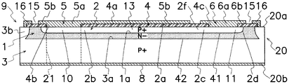
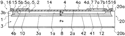
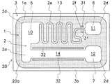
本実施の形態の半導体装置は、図1〜図3に示すように、N−型半導体領域を構成する第1の半導体領域(1)と、第1の半導体領域(1)とは異なる導電型により第1の半導体領域(1)の主面(1a)上に隣接して形成されたP+型半導体領域を構成する第2の半導体領域(2)と、第1の半導体領域(1)とは異なる導電型により第1の半導体領域(1)の主面(1a)とは反対側の他面に隣接して形成されたP+型半導体領域の第3の半導体領域(3)とを有する半導体層(20)を備え、半導体層(20)の主面(20a)とは反対側の底面(20b)には、接地電極(8)が形成される。従って、第2の半導体領域(2)と第3の半導体領域(3)とは互いに同一の導電型であり、第2の半導体領域(2)及び第3の半導体領域(3)と第1の半導体領域(1)とは異なる導電型である。図4及び図5に示すように、互いに離間して形成された第1〜第3の開口部(4b〜4d)を有する絶縁膜(4)は、半導体層(20)の主面(20a)を被覆する。
Hereinafter, an embodiment of a semiconductor device including a bidirectional diode according to the present invention will be described with reference to FIGS.
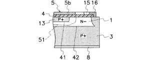
As shown in FIGS. 1 to 3, the semiconductor device of the present embodiment includes a first semiconductor region (1) constituting an N − type semiconductor region and a conductivity type different from that of the first semiconductor region (1). The second semiconductor region (2) constituting the P + type semiconductor region formed adjacent to the main surface (1a) of the first semiconductor region (1) by the first and second semiconductor regions (1) A semiconductor layer having a third semiconductor region (3) of a P + type semiconductor region formed adjacent to the other surface opposite to the main surface (1a) of the first semiconductor region (1) due to different conductivity types The ground electrode (8) is formed on the bottom surface (20b) of the semiconductor layer (20) opposite to the main surface (20a). Therefore, the second semiconductor region (2) and the third semiconductor region (3) have the same conductivity type, and the second semiconductor region (2), the third semiconductor region (3) and the first semiconductor region (3) are the same. The conductivity type is different from that of the semiconductor region (1). As shown in FIGS. 4 and 5, the insulating film (4) having the first to third openings (4b to 4d) formed to be separated from each other is formed on the main surface (20a) of the semiconductor layer (20). Coating.
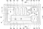
図4に示すように、第1〜第3の電極(5〜7)は縁部導体(16)から間隙部(15)を介して離間した位置に配置される。第2の半導体領域(2)には第1の領域(10)、第2の領域(11)及び第3の領域(12)が互いに離間して形成され、第1〜第3の領域(10〜12)の各曲部には電界集中を緩和する湾曲接合部(2d)が設けられる。第1の電極(5)は、絶縁膜(4)の第1の開口部(4b)を通じて第2の半導体領域(2)の第1の領域(10)に電気的に接続され、第2の電極(6)は、絶縁膜(4)の第2の開口部(4c)を通じて第2の半導体領域(2)の第2の領域(11)に電気的に接続される。同様に、第3の電極(7)は、絶縁膜(4)の第3の開口部(4d)を通じて第2の半導体領域(2)の第3の領域(12)に電気的に接続される。第1の領域(10)と第2の領域(11)は、第2の半導体領域(2)によって形成された第1の抵抗領域(13)を通じて電気的に接続され、第1の領域(10)と第3の領域(12)は、第2の半導体領域(2)によって形成された第2の抵抗領域(14)により電気的に接続される。 As shown in FIG. 4, the first to third electrodes (5 to 7) are arranged at positions spaced from the edge conductor (16) via the gap (15). In the second semiconductor region (2), a first region (10), a second region (11), and a third region (12) are formed to be separated from each other, and the first to third regions (10 The curved joints (2d) that alleviate the electric field concentration are provided in each of the curved parts (12) to (12). The first electrode (5) is electrically connected to the first region (10) of the second semiconductor region (2) through the first opening (4b) of the insulating film (4), and the second electrode The electrode (6) is electrically connected to the second region (11) of the second semiconductor region (2) through the second opening (4c) of the insulating film (4). Similarly, the third electrode (7) is electrically connected to the third region (12) of the second semiconductor region (2) through the third opening (4d) of the insulating film (4). . The first region (10) and the second region (11) are electrically connected through the first resistance region (13) formed by the second semiconductor region (2), and the first region (10 ) And the third region (12) are electrically connected by the second resistance region (14) formed by the second semiconductor region (2).
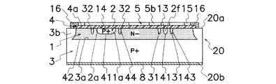
図5に示すように、第2の半導体領域(2)の第1の領域(10)と第2の領域(11)との間を接続する第1の抵抗領域(13)は、第1の領域(10)に接続された蛇行部(2e)と、蛇行部(2e)と第2の領域(11)との間に接続された直線状部(2f)とを有する。第1の抵抗領域(13)が幅狭の帯状の蛇行部(2e)を有することで、第1の領域(10)と第2の領域(11)との間に所望の長さを有する第1の抵抗領域(13)を比較的小さな占有面積で形成できる。このため、比較的小さな占有面積で第1の抵抗領域(13)に所要の高い抵抗値を付与することができる。また、第1の領域(10)と第3の領域(12)との間を接続する第2の抵抗領域(14)は、第1の抵抗領域(13)より幅が広く且つ直線的に延伸する帯状に形成される。このため、第2の抵抗領域(14)は、第1の抵抗領域(13)より低い抵抗値を有する。
As shown in FIG. 5, the first resistance region (13) connecting the first region (10) and the second region (11) of the second semiconductor region (2) is the first region. The meandering portion (2e) connected to the region (10) and the linear portion (2f) connected between the meandering portion (2e) and the second region (11). Since the first resistance region (13) has the narrow belt-like meandering portion (2e), the first resistance region (13) has a desired length between the first region (10) and the second region (11). One
本実施の形態では、複数回屈曲する幅狭の帯状に形成される第1の抵抗領域(13)は相対的に高い抵抗値、例えば5kΩに設定され、直線的な幅広の帯状に形成される第2の抵抗領域(14)は相対的に低い抵抗値、例えば240Ωに設定される。
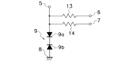
通常の動作時には第1及び第2の領域(10,11)間と第1及び第3の領域(10,12)間の抵抗素子が動作し、過電圧が印加された時は図6に示す双方向ダイオード(9)がオンしてバックメタルとしての接地電極(8)を通じて電流を流すことができる。第1の抵抗領域(13)及び第2の抵抗領域(14)の抵抗値は、第1及び第2の抵抗領域(13,14)を構成する第2の半導体領域(2)の幅、長さ及び深さ並びに不純物濃度により適宜設定し又は調整することができる。
In the present embodiment, the
During normal operation, the resistance elements operate between the first and second regions (10, 11) and between the first and third regions (10, 12). When an overvoltage is applied, both elements shown in FIG. The direction diode (9) is turned on, and a current can flow through the ground electrode (8) as a back metal. The resistance values of the first resistance region (13) and the second resistance region (14) are the width and length of the second semiconductor region (2) constituting the first and second resistance regions (13, 14). It can be set or adjusted as appropriate according to the depth, depth, and impurity concentration.
絶縁膜(4)は、例えば半導体層(20)の主面(20a)を熱酸化して形成されたシリコン酸化膜(SiO2)から成り、第1〜第3の領域(10〜12)と第1〜第3の電極(5〜7)とを電気的に接続する3つの開口部(4b〜4d)が形成される。開口部(4b〜4d) が形成された絶縁膜(4)は、第1の半導体領域(1)、第2の半導体領域(2)及び第3の半導体領域(3)が露出する半導体層(20)の主面(20a)を被覆し、絶縁膜(4)を介して互いに離間して配置される第1の電極(5)、第2の電極(6)及び第3の電極(7)は、各開口部(4b)を通じて第2の半導体領域(2)の第1の領域(10)、第2の領域(11)及び第3の領域(12)にそれぞれ電気的に接続される。 The insulating film (4) is made of, for example, a silicon oxide film (SiO 2 ) formed by thermally oxidizing the main surface (20a) of the semiconductor layer (20), and the first to third regions (10 to 12) and Three openings (4b to 4d) for electrically connecting the first to third electrodes (5 to 7) are formed. The insulating film (4) in which the openings (4b to 4d) are formed is a semiconductor layer (1) in which the first semiconductor region (1), the second semiconductor region (2) and the third semiconductor region (3) are exposed. The first electrode (5), the second electrode (6) and the third electrode (7) which cover the main surface (20a) of 20) and are spaced apart from each other via the insulating film (4) Are electrically connected to the first region (10), the second region (11) and the third region (12) of the second semiconductor region (2) through each opening (4b).
図1及び図2に示すように、第1〜第3の電極(5〜7)は、絶縁膜(4)の開口部(4b)を通じて第2の半導体領域(2)の第1〜第3の領域(10〜12)にそれぞれ接触する主電極部(5a〜7a)と、主電極部(5a〜7a)から第2の半導体領域(2)と並行に延伸し且つ絶縁膜(4)を介して第1の半導体領域(1)の主面(1a)を被覆する延長部(5b〜7b)とを備える。第1〜第3の電極(5〜7)は例えば周知のアルミニウム(Al)蒸着等の方法により形成される。第1の電極(5)は一方のダイオード(9a)のアノード電極、第1の抵抗領域(13)の一端の電極及び第2の抵抗領域(14)の一端の電極を構成する。また、第2の電極(6)は第1の抵抗領域(13)の他端の電極を構成し、第3の電極(7)は第2の抵抗領域(14)の他端の電極を構成する。図4に示すように、第2の半導体領域(2)に形成された第1の抵抗領域(13)の蛇行部(2e)は、絶縁膜(4)を介して第1の電極(5)の延長部(5b)により被覆される。このため、第1の電極(5)の延長部(5b)が放熱体として良好に機能し、第1の抵抗領域(13)で発生した熱を延長部(5b)を通じて外部へ放出することができる。この結果、抵抗値の変動や半導体素子の特性変動を良好に防止することができる。 As shown in FIGS. 1 and 2, the first to third electrodes (5 to 7) are connected to the first to third electrodes of the second semiconductor region (2) through the opening (4b) of the insulating film (4). Main electrode portions (5a to 7a) that respectively contact the regions (10 to 12), and the main electrode portions (5a to 7a) extending in parallel with the second semiconductor region (2) and the insulating film (4) And an extension (5b-7b) covering the main surface (1a) of the first semiconductor region (1). The first to third electrodes (5 to 7) are formed by a known method such as aluminum (Al) deposition. The first electrode (5) constitutes an anode electrode of one diode (9a), an electrode at one end of the first resistance region (13), and an electrode at one end of the second resistance region (14). The second electrode (6) constitutes an electrode at the other end of the first resistance region (13), and the third electrode (7) constitutes an electrode at the other end of the second resistance region (14). To do. As shown in FIG. 4, the meandering portion (2e) of the first resistance region (13) formed in the second semiconductor region (2) is connected to the first electrode (5) via the insulating film (4). It is covered with an extension (5b). For this reason, the extension part (5b) of the first electrode (5) functions well as a radiator, and the heat generated in the first resistance region (13) can be released to the outside through the extension part (5b). it can. As a result, resistance value fluctuations and semiconductor element characteristic fluctuations can be satisfactorily prevented.
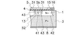
また、図3〜図5に示すように、第1の電極(5)の延長部(5b)と第2の電極(6)との間に介在する第1の抵抗領域(13)の直線状部(2f)の外側には、直線状部(2f)から離間して第1の電界緩和領域(31)が形成されている。更に、図3〜図5に示すように、第1の電極(5)と第3の電極(7)との間に介在する第2の抵抗領域(14)の外側には、第2の抵抗領域(14)から離間して第2の電界緩和領域(32)が形成されている。第1の電界緩和領域(31)及び第2の電界緩和領域(32)は、第2の半導体領域(2)と同一の導電型のP+型半導体領域から成る。 As shown in FIGS. 3 to 5, the first resistance region (13) linearly interposed between the extension (5b) of the first electrode (5) and the second electrode (6). A first electric field relaxation region (31) is formed outside the portion (2f) and spaced from the linear portion (2f). Further, as shown in FIGS. 3 to 5, a second resistor is provided outside the second resistor region (14) interposed between the first electrode (5) and the third electrode (7). A second electric field relaxation region (32) is formed apart from the region (14). The first electric field relaxation region (31) and the second electric field relaxation region (32) are composed of a P + type semiconductor region having the same conductivity type as the second semiconductor region (2).
図1〜図3に示すように、第3の半導体領域(3)は、第1の半導体領域(1)に隣接して、半導体層(20)の主面(20a)に向けて下面から上方に広がる傾斜縁部(3b)を有する。第3の半導体領域(3)の傾斜縁部(3b)は、図5に示すように、第1の半導体領域(1)の外周縁を包囲して枠状に形成される。傾斜縁部(3b)の上面には、縁部導体(16)が接続されている。図1〜図3に示すように、第2の半導体領域(2)と第3の半導体領域(3)との間に第1の半導体領域(1)が形成されるので、第1の半導体領域(1)の主面(1a)に第2の半導体領域(2)が接触し、第1の半導体領域(1)の主面(1a)とは反対側の他面及び外周部に第3の半導体領域(3)の主面(3a)及びその傾斜縁部(3b)が接触する。第3の半導体領域(3)の主面(3a)とは反対側の他面は、半導体層(20)の他面(20b)として接地電極(8)に電気的に接続される。接地電極(8)は、例えばアルミニウム(Al)等から成る金属膜を半導体層(20)の他面(20b)にスパッタリング又は真空蒸着することにより形成することができる。 As shown in FIGS. 1 to 3, the third semiconductor region (3) is adjacent to the first semiconductor region (1) and upward from the lower surface toward the main surface (20 a) of the semiconductor layer (20). And an inclined edge (3b) extending in the direction. As shown in FIG. 5, the inclined edge portion (3b) of the third semiconductor region (3) is formed in a frame shape so as to surround the outer peripheral edge of the first semiconductor region (1). An edge conductor (16) is connected to the upper surface of the inclined edge (3b). As shown in FIGS. 1 to 3, since the first semiconductor region (1) is formed between the second semiconductor region (2) and the third semiconductor region (3), the first semiconductor region The second semiconductor region (2) is in contact with the main surface (1a) of (1), and the third surface is formed on the other surface and the outer periphery of the first semiconductor region (1) opposite to the main surface (1a). The main surface (3a) of the semiconductor region (3) and its inclined edge (3b) are in contact. The other surface of the third semiconductor region (3) opposite to the main surface (3a) is electrically connected to the ground electrode (8) as the other surface (20b) of the semiconductor layer (20). The ground electrode (8) can be formed, for example, by sputtering or vacuum depositing a metal film made of aluminum (Al) or the like on the other surface (20b) of the semiconductor layer (20).
図1に示すように、第1の半導体領域(1)と第2の半導体領域(2)との界面には第1のPN接合(41)が形成され、第1の半導体領域(1)と第3の半導体領域(3)との界面には第2のPN接合(42)が形成されるため、主として破線部(21)で示す領域に第1の電極(5)から接地電極(8)に向かう半導体層(20)の深さ方向に能動素子としての双方向ダイオード(9)のPNP構造が形成される。即ち、双方向ダイオード(9)は、図6に示すように互いに逆極性に接続された一方のダイオード(9a)と他方のダイオード(9b)とを有し、一方のダイオード(9a)はアノード領域を形成する第2の半導体領域(2)とカソード領域を形成する第1の半導体領域(1)とにより構成され、他方のダイオード(9b)はアノード領域を形成する第3の半導体領域(3)とカソード領域を形成する第1の半導体領域(1)とにより構成される。
図3に示すように、第1の半導体領域(1)と第1の電界緩和領域(31)との界面には第3のPN接合(43)が形成され、第1の半導体領域(1)と第2の電界緩和領域(32)との界面には第4のPN接合(44)が形成される。
As shown in FIG. 1, a first PN junction (41) is formed at the interface between the first semiconductor region (1) and the second semiconductor region (2), and the first semiconductor region (1) and Since the second PN junction (42) is formed at the interface with the third semiconductor region (3), the first electrode (5) to the ground electrode (8) mainly in the region indicated by the broken line portion (21). A PNP structure of a bidirectional diode (9) as an active element is formed in the depth direction of the semiconductor layer (20) toward the surface. That is, as shown in FIG. 6, the bidirectional diode (9) has one diode (9a) and the other diode (9b) connected in opposite polarities, and the one diode (9a) is an anode region. The second semiconductor region (2) forming the cathode region and the first semiconductor region (1) forming the cathode region, and the other diode (9b) is the third semiconductor region (3) forming the anode region. And a first semiconductor region (1) forming a cathode region.
As shown in FIG. 3, a third PN junction (43) is formed at the interface between the first semiconductor region (1) and the first electric field relaxation region (31), and the first semiconductor region (1). A fourth PN junction (44) is formed at the interface between the first electric field relaxation region (32) and the second electric field relaxation region (32).
第1の半導体領域(1)と第2の半導体領域(2)との界面に形成された第1のPN接合(41)に逆方向電圧が印加されたとき、第1のPN接合(41)から空乏層が広がる。この空乏層は、第1〜第3の電極(5〜7)の延長部(5b〜7b)によって構成されるフィールドプレートによって、第1の半導体領域(1)内に良好に広げられる。即ち、図1に示すように、第2の電極(6)は、主電極部(6a)から第2の半導体領域(2)と並行に延伸し且つ絶縁膜(4)を介して第1の半導体領域(1)の主面(1a)を被覆する延長部(6b)を有し、延長部(6b)は、第1の電極(5)の延長部(5b)と同様にフィールドプレートを形成する。同様に、第3の電極(7)は、主電極部(7a)から第2の半導体領域(2)と並行に延伸し且つ絶縁膜(4)を介して第1の半導体領域(1)の主面(1a)を被覆する延長部(6b)を有し、延長部(6b)は、第1の電極(5)の延長部(5b)と同様にフィールドプレートを形成する。 When a reverse voltage is applied to the first PN junction (41) formed at the interface between the first semiconductor region (1) and the second semiconductor region (2), the first PN junction (41) The depletion layer spreads out. This depletion layer is satisfactorily spread in the first semiconductor region (1) by the field plate constituted by the extensions (5b to 7b) of the first to third electrodes (5 to 7). That is, as shown in FIG. 1, the second electrode (6) extends in parallel with the second semiconductor region (2) from the main electrode portion (6a) and passes through the insulating film (4). The extension portion (6b) covers the main surface (1a) of the semiconductor region (1), and the extension portion (6b) forms a field plate similarly to the extension portion (5b) of the first electrode (5). To do. Similarly, the third electrode (7) extends in parallel with the second semiconductor region (2) from the main electrode portion (7a) and extends through the insulating film (4) to the first semiconductor region (1). The extension portion (6b) covers the main surface (1a), and the extension portion (6b) forms a field plate in the same manner as the extension portion (5b) of the first electrode (5).
また、第1〜第3の電極(5〜7)の延長部(5b〜7b)によって構成されるフィールドプレートの効果が及ばない領域には、FLRとして機能する第1の電界緩和領域(31)と第2の電界緩和領域(32)が形成されており、フィールドプレートによる電界集中緩和効果が補完されている。即ち、第1の電極(5)の延長部(5b)と第2の電極(6)の延長部(6b)との間には第1の電界緩和領域(31)が形成されており、第1の電極(5)の延長部(5b)及び第3の電極(7)の延長部(7b)との間には第2の電界緩和領域(32)が形成されている。このため、第1のPN接合(41)から広がる空乏層が、第1の半導体領域(1)と第1の電界緩和領域(31)との界面に形成された第3のPN接合(43)及び第1の半導体領域(1)と第2の電界緩和領域(32)との界面に形成された第4のPN接合(44)に到達すると、第3のPN接合(43)及び第4のPN接合(44)からも空乏層が広がり、空乏層のカーバチャ(曲率)を緩和することができる。この結果、第1のPN接合(41)の全周にわたって、電界集中を良好に緩和できる連続した空乏層を形成することができる。 The first electric field relaxation region (31) functioning as an FLR is provided in a region where the effect of the field plate constituted by the extension portions (5b to 7b) of the first to third electrodes (5 to 7) does not reach. And a second electric field relaxation region (32) are formed to complement the electric field concentration relaxation effect of the field plate. That is, a first electric field relaxation region (31) is formed between the extension (5b) of the first electrode (5) and the extension (6b) of the second electrode (6). A second electric field relaxation region (32) is formed between the extension (5b) of the first electrode (5) and the extension (7b) of the third electrode (7). Therefore, the third PN junction (43) in which a depletion layer extending from the first PN junction (41) is formed at the interface between the first semiconductor region (1) and the first electric field relaxation region (31). When the fourth PN junction (44) formed at the interface between the first semiconductor region (1) and the second electric field relaxation region (32) is reached, the third PN junction (43) and the fourth PN junction (43) A depletion layer also extends from the PN junction (44), and the curvature (curvature) of the depletion layer can be relaxed. As a result, a continuous depletion layer capable of satisfactorily relieving electric field concentration can be formed over the entire circumference of the first PN junction (41).
半導体層(20)は、第3の半導体領域(3)を構成する厚さ200〜300μm程度のP+型シリコン基板を出発母材として形成され、この基板の上面に、例えば厚さ40μm程度の第1の半導体領域(1)をエピタキシャル成長で形成させる。次に、図示しないが周知のフォトリソグラフィ技術により所定の形状を有する拡散マスクを基板の主面に被覆する。拡散マスクに形成された開口には、第1〜第3の領域(10〜12)、第1及び第2の抵抗領域(13,14)及び第1及び第2の電界緩和領域(31,32)を形成する部分の第1の半導体領域(1)の上面が露出する。続いて、拡散マスクの開口を通じて第1の半導体領域(1)の主面(1a)にP型不純物を拡散して15μm程度の厚さで第2の半導体領域(2)と第1及び第2の電界緩和領域(31,32)を形成する。また、第3の半導体領域(3)のうち半導体層(20)の主面(20a)に露出する部分は、N型不純物を拡散して形成する。このように、エピタキシャル成長層により第1の半導体領域(1)を形成すれば、図6に示す双方向ダイオード(9)を構成する2つのダイオード(9a,9b)の耐圧をほぼ等しくすることができる。 The semiconductor layer (20) is formed using a P + type silicon substrate having a thickness of about 200 to 300 μm constituting the third semiconductor region (3) as a starting base material, and a first layer having a thickness of about 40 μm, for example, is formed on the upper surface of the substrate. One semiconductor region (1) is formed by epitaxial growth. Next, although not shown, a main surface of the substrate is covered with a diffusion mask having a predetermined shape by a well-known photolithography technique. The opening formed in the diffusion mask has first to third regions (10 to 12), first and second resistance regions (13, 14), and first and second electric field relaxation regions (31, 32). The upper surface of the portion of the first semiconductor region (1) where the) is to be formed is exposed. Subsequently, P-type impurities are diffused into the main surface (1a) of the first semiconductor region (1) through the opening of the diffusion mask, and the second semiconductor region (2) and the first and second layers are formed to a thickness of about 15 μm. The electric field relaxation regions (31, 32) are formed. Further, the portion of the third semiconductor region (3) exposed to the main surface (20a) of the semiconductor layer (20) is formed by diffusing N-type impurities. Thus, if the first semiconductor region (1) is formed by the epitaxial growth layer, the withstand voltages of the two diodes (9a, 9b) constituting the bidirectional diode (9) shown in FIG. 6 can be made substantially equal. .
本実施の形態の半導体装置では、下記の作用効果が得られる。
[1] 互いに離間して形成される第1の電極(5)と第2の電極(6)との間及び第1の電極(5)と第3の電極(7)との間にそれぞれ介在する第2の半導体領域(2)を異なる抵抗値を有する抵抗素子として使用することができる。
[2] FLRとして機能する第1の電界緩和領域(31)と第2の電界緩和領域(32)によって、フィールドプレートによる電界集中緩和効果が補完され、PN接合(41)の全周にわたって、電界集中を良好に緩和できる曲率の大きい連続的な空乏層を形成することができる。このため、PN接合の高耐圧化を安定して図ることができる。また、フィールドプレート効果が及ばない領域をFLRで補完する構造としたため、高耐圧化構造を比較的小さな占有面積で構築することができる。
[3] 第1及び第2の領域(10,11)間で連続する複数の蛇行部(2e)及び直線状部(2f)を有する第1の抵抗領域(13)に大きな抵抗値を付与することができる。また、第1の抵抗領域(13)の直線状部(2f)から離間して第1の電界緩和領域(31)を形成するので、複数の蛇行部(2e)を互いに隣接して配置でき、半導体層(20)に対する第2の半導体領域(2)の占有面積を比較的小さくすることができる。
[4] 第1の電極(5)の延長部(5b)が蛇行部(2e)の曲部に起こる電界集中を良好に緩和するフィールドプレートとして作用するので、第2の半導体領域(2)を相対的に幅狭に且つ小さな曲率で形成することができ、高い抵抗値を有し且つ高耐圧の第1の抵抗領域(13)を比較的小さな占有面積で形成できる。
[5] 半導体層(20)の深さ方向に能動素子を形成し、半導体層(20)の主面(20a)と並行な方向に抵抗素子を形成するので、半導体装置を大型化せずに、高耐圧の半導体装置を形成できる。
[6] 一方のダイオード(9a)のアノード領域の一部として第1及び第2の抵抗領域(13,14)を作用させて、双方向ダイオードの電流容量を増大させることができる。
[7] 相対的に抵抗値の高い第1の抵抗領域(13)を屈曲形状で形成したので、1つの半導体層(20)内に抵抗値の高い第1の抵抗領域(13)と抵抗値の低い第2の抵抗領域(14)とを集積できると共に、その占有面積を十分に小さくすることができる。
In the semiconductor device of the present embodiment, the following operational effects can be obtained.
[1] Intervene between the first electrode (5) and the second electrode (6) formed apart from each other and between the first electrode (5) and the third electrode (7), respectively. The second semiconductor region (2) to be used can be used as a resistance element having a different resistance value.
[2] The electric field concentration relaxation effect by the field plate is complemented by the first electric field relaxation region (31) and the second electric field relaxation region (32) functioning as the FLR, and the electric field is spread over the entire circumference of the PN junction (41) It is possible to form a continuous depletion layer having a large curvature that can relax the concentration well. For this reason, the high breakdown voltage of the PN junction can be stably achieved. In addition, since the region where the field plate effect does not reach is structured to be complemented by FLR, a high breakdown voltage structure can be constructed with a relatively small occupied area.
[3] Giving a large resistance value to the first resistance region (13) having a plurality of meandering portions (2e) and linear portions (2f) continuous between the first and second regions (10, 11). be able to. Further, since the first electric field relaxation region (31) is formed apart from the linear portion (2f) of the first resistance region (13), a plurality of meandering portions (2e) can be arranged adjacent to each other, The area occupied by the second semiconductor region (2) with respect to the semiconductor layer (20) can be made relatively small.
[4] Since the extension part (5b) of the first electrode (5) acts as a field plate that satisfactorily relaxes the electric field concentration occurring at the curved part of the meandering part (2e), the second semiconductor region (2) is formed. The first resistance region (13) having a relatively narrow width and a small curvature and having a high resistance value and a high breakdown voltage can be formed with a relatively small occupation area.
[5] Since the active element is formed in the depth direction of the semiconductor layer (20) and the resistance element is formed in a direction parallel to the main surface (20a) of the semiconductor layer (20), the semiconductor device is not enlarged. A high breakdown voltage semiconductor device can be formed.
[6] The current capacity of the bidirectional diode can be increased by causing the first and second resistance regions (13, 14) to act as part of the anode region of one diode (9a).
[7] Since the first resistance region (13) having a relatively high resistance value is formed in a bent shape, the first resistance region (13) having a high resistance value and the resistance value are formed in one semiconductor layer (20). The second resistance region (14) having a low level can be integrated, and the occupied area can be sufficiently reduced.
本発明の実施態様は前記の実施の形態に限定されず、種々の変更が可能である。例えば、3つ以上の抵抗領域(13,14)を第2の半導体領域(2)に設けてもよい。また、図示の波形パターンに限らず、半導体基板の形状又は抵抗値の設定等の諸条件により渦巻状等の様々な形状に第1の抵抗領域(13)を形成することが可能である。また、図示の一重の第1及び第2の電界緩和領域(31,32)に限定されず、二重以上の電界緩和領域を設けてもよい。更に、図6に示す抵抗値の異なる2つの抵抗領域(13,14)を備えた双方向ダイオードについて上記の実施の形態を説明したが、単方向ダイオード、サイリスタ、トランジスタ又はパワーIC等の異なる形態のPN接合を有する半導体素子を備えた半導体装置にも本発明を適用することができる。また、第1の電界緩和領域(31)を第1の電極(5)の延長部(5b)の側面側まで延伸させても良い。 Embodiments of the present invention are not limited to the above-described embodiments, and various modifications can be made. For example, three or more resistance regions (13, 14) may be provided in the second semiconductor region (2). In addition, the first resistance region (13) can be formed in various shapes such as a spiral shape depending on various conditions such as the shape of the semiconductor substrate or the setting of the resistance value, without being limited to the illustrated waveform pattern. Further, the electric field relaxation regions are not limited to the single first and second electric field relaxation regions (31, 32) shown in the drawing, and double or more electric field relaxation regions may be provided. Furthermore, although the above embodiment has been described for the bidirectional diode having two resistance regions (13, 14) having different resistance values shown in FIG. 6, different forms such as a unidirectional diode, a thyristor, a transistor, or a power IC are described. The present invention can also be applied to a semiconductor device including a semiconductor element having a PN junction. Moreover, you may extend the 1st electric field relaxation area | region (31) to the side surface side of the extension part (5b) of a 1st electrode (5).
本発明は、抵抗値の高い拡散抵抗を比較的小さい占有面積で集積でき、且つ素子の耐圧向上に効果が顕著である。 The present invention can integrate diffused resistors having a high resistance value with a relatively small occupied area, and is remarkable in improving the breakdown voltage of the element.
(1)・・第1の半導体領域(N−型半導体領域)、 (1a)・・主面、 (2)・・第2の半導体領域(P+型半導体領域)、 (2a)・・主面、 (2b)・・一端、 (2c)・・他端、 (2d)・・湾曲接合部、 (2e)・・蛇行部、 (2f)・・直線状部、 (3)・・第3の半導体領域(P+型半導体領域)、 (3a)・・主面、 (3b)・・傾斜縁部、 (4)・・絶縁膜、 (4a)・・主面、 (4b〜4d)・・開口部、 (5〜7)・・第1〜第3の電極、 (5a〜7a)・・主電極部、 (5b〜7b)・・延長部、 (8)・・接地電極、 (9)・・双方向ダイオード、 (9a)・・一方のダイオード、 (9b)・・他方のダイオード、 (10〜12)・・第1〜第3の領域、 (13)・・第1の抵抗領域、 (14)・・第2の抵抗領域、 (15)・・間隙部、 (16)・・縁部導体、 (20)・・半導体層、 (20a)・・主面、 (20b)・・他面、 (21)・・破線部、 (31)・・第1の電界緩和領域、 (32)・・第2の電界緩和領域、 (41〜44)・・第1〜第4のPN接合、 (51,52)・・空乏層 (1) ・ ・ First semiconductor region (N− type semiconductor region), (1a) ・ ・ Main surface, (2) ・ ・ Second semiconductor region (P + type semiconductor region), (2a) ・ ・ Main surface・ (2b) ・ ・ One end, (2c) ・ ・ Other end, (2d) ・ ・ Curved joint, (2e) ・ ・ Meandering part, (2f) ・ ・ Linear part, (3) ・ ・ Third Semiconductor region (P + type semiconductor region), (3a) ·· Main surface, (3b) · · Inclined edge, (4) · · Insulating film, (4a) · · Main surface, (4b to 4d) · · Opening Part, (5-7) .. First to third electrodes, (5a-7a) .. Main electrode part, (5b-7b) .. Extension part, (8) .. Ground electrode, (9). -Bidirectional diode (9a)-One diode (9b)-Other diode (10-12)-First to third regions (13)-First resistance region ( 14) ・ ・ Second resistance region, (15) ・ ・ Gap, (16) ・ ・ Edge conductor, (20) ・ ・ Semiconductor layer, (20a) ・ ・ Main surface, (20b) ・ ・ Other surface , (21) ... ··· First electric field relaxation region, (32) · · Second electric field relaxation region, (41 to 44) · · First to fourth PN junctions, (51,52) · · Depletion layer
Claims (5)
第1及び第2の開口部をもって前記半導体層の主面を被覆する絶縁膜と、
該絶縁膜を介して前記半導体層の主面上に互いに離間して形成される第1の電極及び第2の電極とを備え、
前記第2の半導体領域は、前記第1の開口部内の前記第1の電極に電気的に接続される第1の領域と、前記第2の開口部内の前記第2の電極に電気的に接続される第2の領域と、前記第1の領域と前記第2の領域との間に形成される抵抗領域とを有し、
前記第1の電極は、前記絶縁膜の第1の開口部内に配置されて前記第2の半導体領域の主面に接触する主電極部と、該主電極部に接続され且つ前記絶縁膜を介して前記第2の半導体領域の抵抗領域を被覆する延長部とを有し、
前記第2の電極は、前記絶縁膜の第2の開口部内に配置されて前記第2の半導体領域の主面に接触する主電極部を有し、
前記第2の半導体領域と同一の導電型の半導体領域から成る電界緩和領域を前記第2の半導体領域から離間して且つ前記第1の電極の延長部と前記第2の電極との間に形成し、前記電界緩和領域により、空乏層を連続的に形成して、前記第1の半導体領域と前記第2の半導体領域との界面に形成されるPN接合の電界集中を緩和することを特徴とする半導体装置。 A semiconductor layer having a first semiconductor region and a second semiconductor region formed on a part of the surface of the first semiconductor region with a conductivity type different from that of the first semiconductor region;
An insulating film covering the main surface of the semiconductor layer with the first and second openings;
A first electrode and a second electrode formed on the main surface of the semiconductor layer via the insulating film and spaced apart from each other;
The second semiconductor region is electrically connected to the first region electrically connected to the first electrode in the first opening and to the second electrode in the second opening. A second region, and a resistance region formed between the first region and the second region,
The first electrode is disposed in the first opening of the insulating film and is in contact with the main surface of the second semiconductor region, and is connected to the main electrode and via the insulating film Extending the resistance region of the second semiconductor region,
The second electrode has a main electrode portion disposed in the second opening of the insulating film and in contact with the main surface of the second semiconductor region,
An electric field relaxation region composed of a semiconductor region of the same conductivity type as the second semiconductor region is formed apart from the second semiconductor region and between the extension of the first electrode and the second electrode. A depletion layer is continuously formed by the electric field relaxation region to reduce electric field concentration of a PN junction formed at an interface between the first semiconductor region and the second semiconductor region. Semiconductor device.
該延長部は、前記絶縁膜を介して前記第1の半導体領域の主面を被覆する請求項1に記載の半導体装置。 The second electrode has an extension extending from the main electrode portion in parallel with the second semiconductor region,
The semiconductor device according to claim 1, wherein the extension part covers a main surface of the first semiconductor region via the insulating film.
前記半導体層は、前記第1の半導体領域とは異なる導電型により形成される第3の半導体領域を有し、
前記第2の半導体領域は、前記絶縁膜に形成される第3の開口部内の前記第3の電極に電気的に接続される第3の領域を有し、
前記第1の半導体領域と前記第2の半導体領域との界面に第1のPN接合を形成し、
前記第3の半導体領域内に形成される前記第1の半導体領域と前記第3の半導体領域との界面に第2のPN接合を形成し、
前記第1の電極から前記接地電極に向かう前記半導体層の深さ方向に双方向ダイオードを形成した請求項1又は2に記載の半導体装置。 A third electrode formed on the main surface of the semiconductor layer via the insulating film and spaced from the first electrode and the second electrode; and the semiconductor on the opposite side of the main surface of the semiconductor layer A ground electrode formed on the bottom surface of the layer,
The semiconductor layer has a third semiconductor region formed with a conductivity type different from that of the first semiconductor region;
The second semiconductor region has a third region electrically connected to the third electrode in a third opening formed in the insulating film,
Forming a first PN junction at an interface between the first semiconductor region and the second semiconductor region;
Forming a second PN junction at an interface between the first semiconductor region and the third semiconductor region formed in the third semiconductor region;
The semiconductor device according to claim 1, wherein a bidirectional diode is formed in a depth direction of the semiconductor layer from the first electrode toward the ground electrode.
前記第1の電極と第2の電極とは、前記蛇行部及び直線状部を通じて互いに電気的に接続され、
前記蛇行部は、前記絶縁膜を介して前記第1の電極の延長部により被覆され、
前記電界緩和領域は、前記直線状部の両側に且つ該直線状部から離間して前記第1の半導体領域内に形成される請求項3に記載の半導体装置。 The second semiconductor region has a meandering portion serving as the resistance region connected to the first region, and a linear portion connected between the meandering portion and the second region,
The first electrode and the second electrode are electrically connected to each other through the meandering portion and the linear portion,
The meandering portion is covered with an extension of the first electrode through the insulating film,
The semiconductor device according to claim 3, wherein the electric field relaxation region is formed in the first semiconductor region on both sides of the linear portion and apart from the linear portion.
前記電界緩和領域は、フィールド・リミッティング・リングを構成する請求項1〜4の何れか1項に記載の半導体装置。 The extension of the first electrode constitutes a field plate,
The semiconductor device according to claim 1, wherein the electric field relaxation region constitutes a field limiting ring.
Priority Applications (1)
| Application Number | Priority Date | Filing Date | Title |
|---|---|---|---|
| JP2004010063A JP4697384B2 (en) | 2004-01-19 | 2004-01-19 | Semiconductor device |
Applications Claiming Priority (1)
| Application Number | Priority Date | Filing Date | Title |
|---|---|---|---|
| JP2004010063A JP4697384B2 (en) | 2004-01-19 | 2004-01-19 | Semiconductor device |
Publications (2)
| Publication Number | Publication Date |
|---|---|
| JP2005203658A JP2005203658A (en) | 2005-07-28 |
| JP4697384B2 true JP4697384B2 (en) | 2011-06-08 |
Family
ID=34822893
Family Applications (1)
| Application Number | Title | Priority Date | Filing Date |
|---|---|---|---|
| JP2004010063A Expired - Fee Related JP4697384B2 (en) | 2004-01-19 | 2004-01-19 | Semiconductor device |
Country Status (1)
| Country | Link |
|---|---|
| JP (1) | JP4697384B2 (en) |
Families Citing this family (3)
| Publication number | Priority date | Publication date | Assignee | Title |
|---|---|---|---|---|
| JP4797484B2 (en) * | 2005-07-21 | 2011-10-19 | サンケン電気株式会社 | Semiconductor device having FLR region |
| CN110518061B (en) * | 2019-09-25 | 2024-12-27 | 天津华慧芯科技集团有限公司 | High voltage resistant component and manufacturing process based on planar S-type junction |
| JP7613965B2 (en) * | 2021-03-19 | 2025-01-15 | 新電元工業株式会社 | Semiconductor Device |
Family Cites Families (4)
| Publication number | Priority date | Publication date | Assignee | Title |
|---|---|---|---|---|
| JPS5864059A (en) * | 1981-10-14 | 1983-04-16 | Hitachi Ltd | High withstand resistance element |
| JPH05291241A (en) * | 1992-04-10 | 1993-11-05 | Honda Motor Co Ltd | Semiconductor device |
| JP3732908B2 (en) * | 1996-12-27 | 2006-01-11 | 三洋電機株式会社 | Semiconductor integrated circuit |
| JP2004296803A (en) * | 2003-03-27 | 2004-10-21 | Sanken Electric Co Ltd | Semiconductor device |
-
2004
- 2004-01-19 JP JP2004010063A patent/JP4697384B2/en not_active Expired - Fee Related
Also Published As
| Publication number | Publication date |
|---|---|
| JP2005203658A (en) | 2005-07-28 |
Similar Documents
| Publication | Publication Date | Title |
|---|---|---|
| US4399449A (en) | Composite metal and polysilicon field plate structure for high voltage semiconductor devices | |
| US4412242A (en) | Planar structure for high voltage semiconductor devices with gaps in glassy layer over high field regions | |
| JP4894097B2 (en) | Semiconductor device | |
| CN113161418A (en) | Semiconductor device with a plurality of semiconductor chips | |
| JP2020043241A (en) | Semiconductor device | |
| US5691555A (en) | Integrated structure current sensing resistor for power devices particularly for overload self-protected power MOS devices | |
| JP2004119870A (en) | diode | |
| JP4631268B2 (en) | Semiconductor device | |
| US6703665B1 (en) | Transistor | |
| JP4432332B2 (en) | Semiconductor device and manufacturing method thereof | |
| JP4416288B2 (en) | Reverse conduction thyristor | |
| JP7113386B2 (en) | semiconductor equipment | |
| JP4697384B2 (en) | Semiconductor device | |
| CN114388611B (en) | Semiconductor devices for power | |
| EP0064614B1 (en) | Improved emitter structure for semiconductor devices | |
| JP4576805B2 (en) | Insulated gate semiconductor device and manufacturing method thereof | |
| JP4642767B2 (en) | Surge protection semiconductor device | |
| JP3551154B2 (en) | Semiconductor element | |
| JP4029549B2 (en) | Semiconductor device | |
| JP4797484B2 (en) | Semiconductor device having FLR region | |
| JPH08130317A (en) | Semiconductor device provided with resistive field plate | |
| JP7613965B2 (en) | Semiconductor Device | |
| JP5245280B2 (en) | Semiconductor device | |
| JP2004296803A (en) | Semiconductor device | |
| JPS6327865B2 (en) |
Legal Events
| Date | Code | Title | Description |
|---|---|---|---|
| A621 | Written request for application examination |
Free format text: JAPANESE INTERMEDIATE CODE: A621 Effective date: 20061006 |
|
| A131 | Notification of reasons for refusal |
Free format text: JAPANESE INTERMEDIATE CODE: A131 Effective date: 20101116 |
|
| A521 | Request for written amendment filed |
Free format text: JAPANESE INTERMEDIATE CODE: A523 Effective date: 20110114 |
|
| TRDD | Decision of grant or rejection written | ||
| A01 | Written decision to grant a patent or to grant a registration (utility model) |
Free format text: JAPANESE INTERMEDIATE CODE: A01 Effective date: 20110202 |
|
| A61 | First payment of annual fees (during grant procedure) |
Free format text: JAPANESE INTERMEDIATE CODE: A61 Effective date: 20110215 |
|
| R150 | Certificate of patent or registration of utility model |
Ref document number: 4697384 Country of ref document: JP Free format text: JAPANESE INTERMEDIATE CODE: R150 |
|
| R250 | Receipt of annual fees |
Free format text: JAPANESE INTERMEDIATE CODE: R250 |
|
| R250 | Receipt of annual fees |
Free format text: JAPANESE INTERMEDIATE CODE: R250 |
|
| R250 | Receipt of annual fees |
Free format text: JAPANESE INTERMEDIATE CODE: R250 |
|
| R250 | Receipt of annual fees |
Free format text: JAPANESE INTERMEDIATE CODE: R250 |
|
| R250 | Receipt of annual fees |
Free format text: JAPANESE INTERMEDIATE CODE: R250 |
|
| R250 | Receipt of annual fees |
Free format text: JAPANESE INTERMEDIATE CODE: R250 |
|
| LAPS | Cancellation because of no payment of annual fees |