JP4652829B2 - 電子線露光装置およびデバイス製造方法 - Google Patents
電子線露光装置およびデバイス製造方法 Download PDFInfo
- Publication number
- JP4652829B2 JP4652829B2 JP2005017700A JP2005017700A JP4652829B2 JP 4652829 B2 JP4652829 B2 JP 4652829B2 JP 2005017700 A JP2005017700 A JP 2005017700A JP 2005017700 A JP2005017700 A JP 2005017700A JP 4652829 B2 JP4652829 B2 JP 4652829B2
- Authority
- JP
- Japan
- Prior art keywords
- optical
- photoelectric conversion
- electron beam
- signal
- exposure apparatus
- Prior art date
- Legal status (The legal status is an assumption and is not a legal conclusion. Google has not performed a legal analysis and makes no representation as to the accuracy of the status listed.)
- Expired - Fee Related
Links
Images

Landscapes
- Electron Beam Exposure (AREA)
- Exposure And Positioning Against Photoresist Photosensitive Materials (AREA)
Description
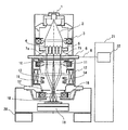
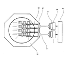
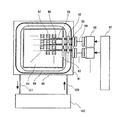
2:電子ビーム
3:コンデンサーレンズ
4:要素電子光学系
5:成形系
6:ブランキングモジュール
7a,7b:中間像
8: 伝送路
10:ブランキングアパーチャ
11:補正レンズ群
12,16:磁気対称ダブレットレンズ(磁界レンズ)
13:磁界偏向器
14:静電偏向器
15:ダイナミックフォーカスコイル
17:制限開口
18:試料
19:XYZステージ
20:マウント
21:制御系
22:ビーム制御部
30:ブランカー基板
31:真空シール
32:ビーム開口
33:ブランキング電極
34:光導波路
35:第2の光電変換部
36:相互接続配線パターン
37:第1の光電変換部
38:配線パターン
39:入力コネクタ
40:駆動信号ケーブル
41:ドライバ
42:データ処理部
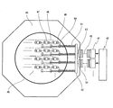
45:信号中継基板
46:真空シール
47:貫通口
48:相互接続配線パターン
49:接合電極
50:第2の光電変換部
51:光導波路
52:第1の光電変換部
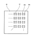
56:ブランカーデバイス基板
57:ビーム開口
58a,58b:ブランキング電極
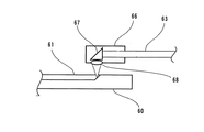
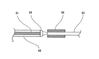
60:ブランカー基板
61:光導波路
62:光カプラー
63:光ファイバーケーブル
64:第1の光電変換部
65:ドライバ
66:ハウジング
67:反射器
68,69:集光レンズ
Claims (6)
- 複数の電子線の照射を個別に制御する複数のブランキング電極と、前記複数のブランキング電極を駆動するための駆動信号を伝送する伝送線路とを有し、前記複数の電子線によって試料にパターンを描画する電子線露光装置において、
前記伝送線路は、第1の基板に形成された光伝送路と、前記光伝送路の始点側で前記駆動信号を電気信号から光信号に変換する第1の光電変換部と、前記第1の光電変換部で変換された光信号を前記光伝送路の終点側で電気信号に変換する複数の第2の光電変換部とを有し、前記複数の第2の光電変換部で変換された電気信号によって前記複数のブランキング電極が制御され、
前記第1の基板には、環状の真空シールが配置され、前記真空シールの内側が真空となり、前記真空シールの外側が大気圧となるように真空隔壁が形成され、前記光伝送路の始点側である前記真空シールの外側に前記第1の光電変換部が配置され、前記光伝送路の終点側である前記真空シールの内側に前記複数の第2の光電変換部が配置されている、
ことを特徴とする電子線露光装置。 - 前記光伝送路は前記第1の基板に形成された光導波路を含む、
ことを特徴とする請求項1に記載の電子線露光装置。 - 前記複数のブランキング電極は、前記第1の基板によって支持された第2の基板に形成され、前記複数のブランキング電極と前記複数の第2の光電変換部とが接合電極を介して接続されている、
ことを特徴とする請求項1または請求項2に記載の電子線露光装置。 - 前記第2の光電変換部は発電素子である、
ことを特徴とする請求項1乃至3の何れか一項に記載の電子線露光装置。 - 前記第1の光電変換部にて変換された光信号を伝送する光ファイバと、前記光導波路の始点に載置され前記光ファイバと結合するための集光レンズを備える光結合器とを有し、前記駆動信号は前記光ファイバを通り、前記光結合器において光ファイバの出力光のスポット径が前記光導波路の大きさに合うように前記集光レンズで集光されて前記光導波路に導入され、前記複数のブランキング電極を駆動する、
ことを特徴とする請求項2乃至4の何れか一項に記載の電子線露光装置。 - 請求項1乃至5の何れか一項に記載の電子線露光装置を用いて、前記試料に露光を行う工程と、露光された前記試料を現像する工程と、を具備することを特徴とするデバイス製造方法。
Priority Applications (1)
| Application Number | Priority Date | Filing Date | Title |
|---|---|---|---|
| JP2005017700A JP4652829B2 (ja) | 2005-01-26 | 2005-01-26 | 電子線露光装置およびデバイス製造方法 |
Applications Claiming Priority (1)
| Application Number | Priority Date | Filing Date | Title |
|---|---|---|---|
| JP2005017700A JP4652829B2 (ja) | 2005-01-26 | 2005-01-26 | 電子線露光装置およびデバイス製造方法 |
Publications (3)
| Publication Number | Publication Date |
|---|---|
| JP2006210460A JP2006210460A (ja) | 2006-08-10 |
| JP2006210460A5 JP2006210460A5 (ja) | 2008-03-06 |
| JP4652829B2 true JP4652829B2 (ja) | 2011-03-16 |
Family
ID=36966989
Family Applications (1)
| Application Number | Title | Priority Date | Filing Date |
|---|---|---|---|
| JP2005017700A Expired - Fee Related JP4652829B2 (ja) | 2005-01-26 | 2005-01-26 | 電子線露光装置およびデバイス製造方法 |
Country Status (1)
| Country | Link |
|---|---|
| JP (1) | JP4652829B2 (ja) |
Families Citing this family (12)
| Publication number | Priority date | Publication date | Assignee | Title |
|---|---|---|---|---|
| TWI300308B (en) * | 2002-10-25 | 2008-08-21 | Mapper Lithography Ip Bv | Lithography system |
| NL2005583C2 (en) | 2009-10-26 | 2014-09-04 | Mapper Lithography Ip Bv | Modulation device and charged particle multi-beamlet lithography system using the same. |
| JP2012023316A (ja) * | 2010-07-16 | 2012-02-02 | Canon Inc | 荷電粒子線描画装置および物品の製造方法 |
| US8921758B2 (en) * | 2010-10-26 | 2014-12-30 | Mapper Lithography Ip B.V. | Modulation device and charged particle multi-beamlet lithography system using the same |
| US8558196B2 (en) * | 2010-11-13 | 2013-10-15 | Mapper Lithography Ip B.V. | Charged particle lithography system with aperture array cooling |
| JP5253532B2 (ja) * | 2011-03-01 | 2013-07-31 | キヤノン株式会社 | 偏向器アレイ、偏向器アレイの製造方法、描画装置、および物品の製造方法 |
| JP6038882B2 (ja) * | 2011-04-20 | 2016-12-07 | マッパー・リソグラフィー・アイピー・ビー.ブイ. | 光ファイバの構成体及びこのような構成体を形成する方法 |
| JP2013008878A (ja) * | 2011-06-24 | 2013-01-10 | Canon Inc | 描画装置、物品の製造方法、及び処理装置 |
| JP5963139B2 (ja) * | 2011-10-03 | 2016-08-03 | 株式会社Param | 電子ビーム描画方法および描画装置 |
| JP6847886B2 (ja) * | 2018-03-20 | 2021-03-24 | 株式会社東芝 | 荷電粒子ビーム偏向デバイス |
| JP7186739B2 (ja) * | 2020-03-11 | 2022-12-09 | 株式会社東芝 | 荷電粒子ビーム偏向デバイス |
| CN116413856B (zh) * | 2023-06-12 | 2024-01-09 | 之江实验室 | 端面耦合器及其制备方法 |
Family Cites Families (7)
| Publication number | Priority date | Publication date | Assignee | Title |
|---|---|---|---|---|
| JPS57204131A (en) * | 1981-06-10 | 1982-12-14 | Toshiba Mach Co Ltd | Electron-ray drawing device |
| JPH0582069A (ja) * | 1991-09-25 | 1993-04-02 | Hitachi Ltd | 電子線描画装置 |
| JP3191998B2 (ja) * | 1992-09-01 | 2001-07-23 | 富士ゼロックス株式会社 | 光通信用波長多重送受信器 |
| JP2001126972A (ja) * | 1999-10-25 | 2001-05-11 | Hitachi Ltd | 電子ビーム描画装置および電子ビームを用いた描画方法 |
| US20020145113A1 (en) * | 2001-04-09 | 2002-10-10 | Applied Materials, Inc. | Optical signal transmission for electron beam imaging apparatus |
| TWI300308B (en) * | 2002-10-25 | 2008-08-21 | Mapper Lithography Ip Bv | Lithography system |
| CN1829945B (zh) * | 2003-07-30 | 2010-05-05 | 迈普尔平版印刷Ip有限公司 | 调制器电路 |
-
2005
- 2005-01-26 JP JP2005017700A patent/JP4652829B2/ja not_active Expired - Fee Related
Also Published As
| Publication number | Publication date |
|---|---|
| JP2006210460A (ja) | 2006-08-10 |
Similar Documents
| Publication | Publication Date | Title |
|---|---|---|
| JP6861683B2 (ja) | 変調装置およびそれを使用する荷電粒子マルチ小ビームリソグラフィシステム | |
| JP4652829B2 (ja) | 電子線露光装置およびデバイス製造方法 | |
| EP2302457B1 (en) | Lithography system | |
| US8841636B2 (en) | Modulation device and charged particle multi-beamlet lithography system using the same | |
| JP6038882B2 (ja) | 光ファイバの構成体及びこのような構成体を形成する方法 | |
| TWI870640B (zh) | 用於操縱電子小射束之透鏡總成 | |
| JP4405867B2 (ja) | 電子線露光装置、および、デバイス製造方法 | |
| KR20010007211A (ko) | 하전 입자 빔 결상 방법, 하전 입자 빔 결상 장치 및 하전입자 빔 노광 장치 | |
| KR101028063B1 (ko) | 마스크리스 리소그래피 시스템 | |
| JP2015070213A (ja) | 描画装置、および物品の製造方法 | |
| TWI506324B (zh) | 光纖的配置及形成此種配置的方法 | |
| JP2008210897A (ja) | 露光装置、及びデバイス製造方法 | |
| KR101293823B1 (ko) | 리소그라피 장치 및 투영 방법 | |
| CN116802764A (zh) | 电子透镜 | |
| JP2013182945A (ja) | 描画装置および物品製造方法 | |
| JP2013143451A (ja) | 描画装置、物品の製造方法及び処理装置 |
Legal Events
| Date | Code | Title | Description |
|---|---|---|---|
| A521 | Request for written amendment filed |
Free format text: JAPANESE INTERMEDIATE CODE: A523 Effective date: 20080121 |
|
| A621 | Written request for application examination |
Free format text: JAPANESE INTERMEDIATE CODE: A621 Effective date: 20080121 |
|
| RD03 | Notification of appointment of power of attorney |
Free format text: JAPANESE INTERMEDIATE CODE: A7423 Effective date: 20090413 |
|
| RD03 | Notification of appointment of power of attorney |
Free format text: JAPANESE INTERMEDIATE CODE: A7423 Effective date: 20090709 |
|
| A977 | Report on retrieval |
Free format text: JAPANESE INTERMEDIATE CODE: A971007 Effective date: 20100909 |
|
| A131 | Notification of reasons for refusal |
Free format text: JAPANESE INTERMEDIATE CODE: A131 Effective date: 20100913 |
|
| A521 | Request for written amendment filed |
Free format text: JAPANESE INTERMEDIATE CODE: A523 Effective date: 20101112 |
|
| TRDD | Decision of grant or rejection written | ||
| A01 | Written decision to grant a patent or to grant a registration (utility model) |
Free format text: JAPANESE INTERMEDIATE CODE: A01 Effective date: 20101203 |
|
| A01 | Written decision to grant a patent or to grant a registration (utility model) |
Free format text: JAPANESE INTERMEDIATE CODE: A01 |
|
| A61 | First payment of annual fees (during grant procedure) |
Free format text: JAPANESE INTERMEDIATE CODE: A61 Effective date: 20101216 |
|
| R150 | Certificate of patent or registration of utility model |
Free format text: JAPANESE INTERMEDIATE CODE: R150 |
|
| FPAY | Renewal fee payment (event date is renewal date of database) |
Free format text: PAYMENT UNTIL: 20131224 Year of fee payment: 3 |
|
| R250 | Receipt of annual fees |
Free format text: JAPANESE INTERMEDIATE CODE: R250 |
|
| LAPS | Cancellation because of no payment of annual fees |