JP4647159B2 - Formation method of electroless plating film - Google Patents
Formation method of electroless plating film Download PDFInfo
- Publication number
- JP4647159B2 JP4647159B2 JP2001288395A JP2001288395A JP4647159B2 JP 4647159 B2 JP4647159 B2 JP 4647159B2 JP 2001288395 A JP2001288395 A JP 2001288395A JP 2001288395 A JP2001288395 A JP 2001288395A JP 4647159 B2 JP4647159 B2 JP 4647159B2
- Authority
- JP
- Japan
- Prior art keywords
- semiconductor substrate
- electroless plating
- film
- electrode
- plating
- Prior art date
- Legal status (The legal status is an assumption and is not a legal conclusion. Google has not performed a legal analysis and makes no representation as to the accuracy of the status listed.)
- Expired - Fee Related
Links
Images
Classifications
-
- H—ELECTRICITY
- H01—ELECTRIC ELEMENTS
- H01L—SEMICONDUCTOR DEVICES NOT COVERED BY CLASS H10
- H01L2224/00—Indexing scheme for arrangements for connecting or disconnecting semiconductor or solid-state bodies and methods related thereto as covered by H01L24/00
- H01L2224/01—Means for bonding being attached to, or being formed on, the surface to be connected, e.g. chip-to-package, die-attach, "first-level" interconnects; Manufacturing methods related thereto
- H01L2224/10—Bump connectors; Manufacturing methods related thereto
- H01L2224/11—Manufacturing methods
Landscapes
- Electrodes Of Semiconductors (AREA)
- Chemically Coating (AREA)
Description
【0001】
【発明の属する技術分野】
本発明は、半導体基板のパッド電極上に選択的、且つ均一にめっき金属を析出させるための無電解めっき皮膜の形成方法に関するものである。
【0002】
【従来の技術】
半導体基板の能動素子面に形成されたアルミニウムを主成分としたパッド電極上に無電解めっきによってバリアメタル、或いは突起電極を形成しようとする場合、該パッド電極上に選択的に、且つ半導体基板上の複数個のパッド電極に対して均一に無電解めっき反応が開始、継続することが要求される。
【0003】
そこで前記パッド電極上に選択的、且つ均一に無電解めっき皮膜を形成するために、そのパッド電極上のみに亜鉛置換処理やパラジウム等の触媒を付与して活性化させる方法が用いられるが、以下に亜鉛置換法を用いた突起電極の形成方法について、図3を参照しながら説明する。
【0004】
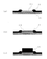
図3(a)〜(e)は、従来の半導体基板の電極形成方法を示した工程断面図である。この工程図は半導体基板上の1個の電極の製造方法について示しているが、この工程において、多数の電極を一度に形成できることを理解されたい。まず、図3(a)に示すように半導体基板15のアルミニウムを主成分とするパッド電極21と、該パッド電極上に開口部を有するパッシベーション膜22が形成される。前記開口部は、大気にさらされると直ぐに自然酸化皮膜が形成されるので、該自然酸化皮膜を酸性液あるいはアルカリ性液に浸漬してエッチング除去する。次に、図3(b)に示すように、半導体基板15の裏面及び側面にめっきレジスト31をスピンコート法で塗布する。これは半導体基板裏面及び側面でのめっき反応を防止するためである。
【0005】
次に、前記めっきレジストが塗布された半導体基板15をアルカリ性あるいは弱酸性の亜鉛酸塩水溶液に浸漬して、図3(c)に示すように、自然酸化皮膜が除去されたパッド電極21表面上に亜鉛置換皮膜23を置換析出させる。必要に応じて希硝酸等に浸漬して一度析出した亜鉛置換皮膜23をエッチング除去した後、再度前記亜鉛酸塩水溶液に浸漬してあらためて2度目の亜鉛置換皮膜を形成させることもある。これは、より均一かつ緻密な亜鉛置換被膜23を得るための手法であり、必要に応じて亜鉛置換皮膜のエッチング工程と亜鉛置換工程がさらに繰り返される場合もある。
【0006】
次いで、半導体基板15を酸化還元型の無電解めっき液に浸漬して、めっき金属によるバリアメタルあるいは突起電極の形成を行うわけであるが、ここでは無電解ニッケルめっきを用いる場合について説明する。図3(d)に示すように、亜鉛置換法の場合、半導体基板15を無電解ニッケルめっき液に浸漬すると、前記亜鉛置換皮膜23が溶解し、パッド電極21表面近傍でニッケルの置換析出が起こり、その後はニッケルの自己触媒作用によって無電解めっき反応が継続し、一定時間浸漬しておくことにより図3(d)のように突起電極16を形成することができる。
【0007】
最後に前記半導体基板15をレジスト剥離液に浸漬して、図3(e)に示すように、半導体基板15の裏面及び側面に塗布しためっきレジスト31を剥離する。
【0008】
【発明が解決しようとする課題】
従来の方法において、半導体基板15の裏面及び側面にめっきレジストを塗布しないで該半導体基板15を無電解めっき液に浸漬した場合、無電解めっき液に対して活性化されていないシリコン等からなる半導体基板15の裏面及び側面では、本来無電解めっき反応は発生しないはずであるが、前記亜鉛置換処理後の水洗が不十分だった場合の亜鉛の残査や無電解めっき液中の浮遊物等が核になって、半導体基板15の裏面及び側面でも無電解めっき反応が発生することがある。しかし、この半導体基板15裏面及び側面は活性化されていないため、均一なめっき皮膜は形成できず、めっきが析出する部位とめっき未着の部位とが生じてしまう。
【0009】
前記、半導体基板15の裏面及び側面で無電解めっき反応が発生した部位では、無電解めっきの酸化還元反応によって部分的な電位の低下が起こり、結果として半導体基板15全体に電位のばらつきを生じさせることとなる。この電位のバラツキは半導体基板15の複数個のパッド電極21にも影響して、これら複数個のパッド電極21上の無電解めっき皮膜の膜厚の不均一、一部のパッド電極21へのめっき不着等の不良が発生し、パッド電極21上への選択性を損なう要因となっていた。
【0010】
たとえ、半導体基板15裏面及び側面へのめっきレジストが塗布された半導体基板15であっても、その半導体基板15の能動素子面のパシベーション膜22下に形成されている内部配線(図示しない)を経由してパッド電極21で発生した電子が移動して、他のパッド電極との間に電位の差を生じさせることがある。この影響により、パッド電極21が負電荷を帯びてしまうのであるが、このパッド電極上へは金属めっきは形成されないので、これもパッド電極21上の無電解めっき皮膜の膜厚の不均一、一部のパッド電極21へのめっき不着等の不良の原因となってしまう。
【0011】
さらに、無電解めっき皮膜が半導体基板15の裏面で成長すると、半導体基板15裏面から側面を経由して半導体基板15の能動素子面のパッシベーション膜22上にもめっき反応が伝搬してしまうので、これもパッド電極21上への選択性を損なう要因となっていた。
【0012】
前記の理由により、従来の方法では半導体基板15裏面及び側面へのめっきレジスト31の塗布は必須であって、その上、このめっきレジスト31はめっき処理後に剥離工程を必要としていた。
【0013】
そこで本発明の目的は、上記従来技術の課題を改良し、半導体基板裏面及び側面にめっきレジストを塗布することなく、該半導体基板の複数個のパッド電極上に均一な無電解めっき皮膜を形成する新規の方法を提供するものである。
【0014】
【課題を解決するための手段】
上記課題を解決するため、本発明においては下記記載の無電解めっき皮膜の形成方法を採用する。
【0015】
すなわち、本発明において上記課題を解決するための第1の手段は、半導体基板のパッド電極上に無電解めっき皮膜を形成する方法であって、半導体基板上にパッド電極と、該パッド電極上に開口部を有するパッシベーション膜を形成し、前記パッド電極上に無電解めっき皮膜を形成する方法であって、そのパッド電極を選択的に活性化する工程と、前記半導体基板と対極とを無電解めっき液に浸漬すると同時に、外部電源により前記半導体基板の裏面側と対極との間に一定の電位を印加しながら無電解めっき皮膜を析出させる工程とを有する。
さらに、第1の手段における、前記活性化する工程が、触媒付与法と亜鉛置換法のいずれかであることが望ましい。また、第1または2の手段における、前記半導体基板に電位を印加しながら無電解めっき皮膜を析出させる工程において、その印加する電位が、めっき金属イオンの酸化還元電位と電解めっき液に使用される還元剤の酸化還元電位との差の値未満の正電位であることが望ましい。
【0016】
(作用)
本発明の無電解めっき皮膜の形成方法は、めっき反応を部分的に抑制したい半導体基板に対して、外部電源から正電位を印加することによって部分的に無電解めっき皮膜の形成を抑制しながら、必要な部分にのみ選択的に無電解めっき皮膜を形成させる方法である。
【0017】
例として次亜燐酸塩を還元剤とした酸化還元型の無電解ニッケルめっきについて説明する。この無電解ニッケルめっきは、次亜燐酸イオンの酸化還元電位である−0.80V(pH5.0、25℃、 NHE基準)とニッケルイオン(Ni2+)の酸化還元電位である−0.25V(pH5.0、25℃、 NHE基準)との差が起電力となり無電解めっき反応が開始、継続される。この起電力を損なわない範囲の微小電位であれば、半導体基板を正電極として外部電源からめっき反応とは逆の電位を印加したとしても無電解めっき反応を継続させることができる。
【0018】
さらに、前記半導体基板内部に形成されている内部配線によって複数個のパッド電極表面に電位差を生じることがあるが、該半導体基板全体に外部電源から微少な電位を印加することにより複数個のパッド電極表面の電位を均一化することができ、均一な膜厚の無電解めっき皮膜を得ることができる。
【0019】
【発明の実施の形態】
本発明による無電解めっき皮膜の形成方法は、半導体基板とその対極となる不溶性電極を無電解めっき液に浸漬して、該半導体基板と該不溶性電極との間に外部電源から一定の電位差を一定時間印加しながら無電解めっき皮膜を形成させる方法である。
【0020】
以下、本発明の無電解めっき皮膜の形成方法による半導体基板の電極形成方法について、図面を用いて説明する。
【0021】
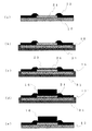
図2(a)に示すように、従来の製造方法と同様に半導体基板15上のアルミニウムを主成分とするパッド電極21と、該パッド電極21上に開口部を有するパッシベーション膜22を形成する。さらにパッド電極21上に形成されている自然酸化皮膜を、酸溶液あるいはアルカリ溶液によってエッチング除去する。そのエッチング液としては、水酸化ナトリウムの希薄溶液や希硫酸を用いることが出来る。酸化皮膜を除去するとともに薄い不働態皮膜を形成させるためには硝酸を用いるのがよい。
【0022】
次に、図2(b)に示すように、酸化皮膜が除去されたパッド電極21上に亜鉛置換法により亜鉛置換皮膜23を置換析出させる。この亜鉛置換法は、イオン化傾向によってアルミニウムが溶出した部位にのみ亜鉛が析出するため、アルミニウムを主成分とするパッド電極21上に選択的に亜鉛置換皮膜を形成させることができる。具体的には、市販のジンケート処理液を用いて室温で30秒から60秒浸漬する。次いで純水洗浄した後、さらに必要に応じて希硝酸等に浸漬して一度析出した亜鉛置換皮膜23をエッチング除去した後、再度前記ジンケート処理液に浸漬して2度目の亜鉛置換皮膜を析出させてもよい。
【0023】
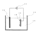
次いで純水で洗浄した後、図1に示すように半導体基板15の裏面側に外部電源11から直流電位を印加しながら、酸化還元型の無電解ニッケルめっき液14に浸漬するわけであるが、本実施例では対極12にステンレスの棒材にニッケルめっきを施したものを用い、対極12を負電極として被めっき基板である半導体基板15に+0.1から0.2Vの正電位を印加しながら無電解ニッケルめっき液14に浸漬することにより、図2(c)に示すような無電解ニッケルめっきによる突起電極16の形成を行った。
【0024】
めっき皮膜の形成速度は従来の方法に比べて遅くなるが、本発明の方法によれば、複数個のパッド電極上に均一なめっき皮膜を形成することができる。尚、対極12にニッケルめっきが析出することとなるが、その反応によりパッド電極21上への無電解ニッケルめっきに影響を与えるものではない。
【0025】
本実施例では、次亜燐酸塩を還元剤とする市販の酸化還元型無電解ニッケルーリン合金めっき液を用い、pH5.0±0.1、90℃、30分の浸漬処理によって、半導体基板15の裏面及び側面にはめっき皮膜を析出させることなく、該半導体基板15の全てのパッド電極21上に均一な5〜6μmのニッケル突起電極を形成させることが出来た。本発明の方法によれば、半導体基板15を無電解めっき液14に浸漬する時間をさらに延長することによって、めっき皮膜がより厚い突起電極16を形成することが可能である。
【0026】
また本実施例では、被メッキ基板である半導体基板15に、対極12に対して正電位を印加して無電解めっきによる突起電極16の形成を行ったが、従来の方法のように半導体基板15の裏面及び側面にめっきレジストを塗布する必要はあるが、半導体基板15の複数個のパッド電極21表面の電位を均一化することのみを目的として、被メッキ基板である半導体基板15に微小の負電位を印加することもできる。
【0027】
また、本発明の手段によれば、無電解めっき液の還元剤の酸化還元電位とめっき金属イオンの酸化還元電位の差の値未満の電位差で、外部電源から半導体基板15へ印加する電位差を選択することにより、パッド電極21上に銅、コバルト、及びその合金等のめっき皮膜も同様に形成することが可能である。
【0028】
さらに、活性化処理として亜鉛以外の他の活性金属を置換させる方法やパラジウム等の触媒を付与する活性化方法を用いても同様に、半導体基板15のパッド電極21上に均一なめっき皮膜を形成することができることは云うまでもない。
【0029】
【発明の効果】
以上のように、本発明によれば半導体基板裏面及び側面へのめっきレジスト塗布、及び後工程での該レジスト剥離工程を不要とし、半導体基板裏面及び側面にめっき皮膜を析出させることなく簡単な操作で半導体基板の複数個のパッド電極上に、均一な膜厚のバリアメタル、或いは突起電極を形成することができる。
【図面の簡単な説明】
【図1】 本発明の無電解めっき皮膜の形成方法を示す模式図である。
【図2】 本発明の半導体基板への電極形成方法を示す工程断面図である。
【図3】 従来の半導体基板への電極形成方法を示す工程断面図である。
【符号の説明】
11 外部電源
12 対極
13 めっき槽
14 無電解めっき液
15 半導体基板
16 突起電極
21 パッド電極
22 パッシベーション膜
23 亜鉛置換皮膜
31 めっきレジスト[0001]
BACKGROUND OF THE INVENTION
The present invention relates to a method for forming an electroless plating film for selectively and uniformly depositing a plating metal on a pad electrode of a semiconductor substrate.
[0002]
[Prior art]
When a barrier metal or a protruding electrode is to be formed by electroless plating on a pad electrode mainly composed of aluminum formed on the active element surface of a semiconductor substrate, selectively on the pad electrode and on the semiconductor substrate It is required that the electroless plating reaction be uniformly started and continued for the plurality of pad electrodes.
[0003]
Therefore, in order to selectively and uniformly form an electroless plating film on the pad electrode, a method of activating by applying a catalyst such as zinc substitution treatment or palladium only on the pad electrode is used. Next, a method for forming a protruding electrode using a zinc substitution method will be described with reference to FIG.
[0004]
3A to 3E are process sectional views showing a conventional method for forming an electrode of a semiconductor substrate. Although this process diagram shows a method for manufacturing one electrode on a semiconductor substrate, it should be understood that a number of electrodes can be formed at one time in this process. First, as shown in FIG. 3A, a
[0005]
Next, the semiconductor substrate 15 coated with the plating resist is immersed in an alkaline or weakly acidic zincate aqueous solution, and the surface of the
[0006]
Next, the semiconductor substrate 15 is immersed in an oxidation-reduction type electroless plating solution to form a barrier metal or protruding electrode using a plating metal. Here, a case where electroless nickel plating is used will be described. As shown in FIG. 3D, in the case of the zinc substitution method, when the semiconductor substrate 15 is immersed in an electroless nickel plating solution, the zinc substitution film 23 is dissolved and nickel substitution deposition occurs near the surface of the
[0007]
Finally, the semiconductor substrate 15 is immersed in a resist stripping solution, and the plating resist 31 applied to the back and side surfaces of the semiconductor substrate 15 is stripped as shown in FIG.
[0008]
[Problems to be solved by the invention]
In a conventional method, when the semiconductor substrate 15 is immersed in an electroless plating solution without applying a plating resist to the back and side surfaces of the semiconductor substrate 15, a semiconductor made of silicon or the like that is not activated with respect to the electroless plating solution The electroless plating reaction should not occur on the back surface and side surface of the substrate 15, but there may be zinc residue or suspended matter in the electroless plating solution when washing with water after the zinc replacement treatment is insufficient. The electroless plating reaction may occur on the back and side surfaces of the semiconductor substrate 15 as a core. However, since the back and side surfaces of the semiconductor substrate 15 are not activated, a uniform plating film cannot be formed, and a portion where plating is deposited and a portion where plating is not deposited are generated.
[0009]
In the portion where the electroless plating reaction has occurred on the back surface and the side surface of the semiconductor substrate 15, a partial potential drop occurs due to the oxidation-reduction reaction of the electroless plating, resulting in potential variations throughout the semiconductor substrate 15. It will be. This variation in potential also affects the plurality of
[0010]
Even if the semiconductor substrate 15 is coated with a plating resist on the back and side surfaces of the semiconductor substrate 15, it passes through internal wiring (not shown) formed under the
[0011]
Further, when the electroless plating film grows on the back surface of the semiconductor substrate 15, the plating reaction is propagated from the back surface of the semiconductor substrate 15 to the
[0012]
For the above reason, in the conventional method, it is essential to apply the plating resist 31 to the back surface and the side surface of the semiconductor substrate 15, and the plating resist 31 requires a peeling process after the plating process.
[0013]
Accordingly, an object of the present invention is to improve the above-described problems of the prior art and form a uniform electroless plating film on a plurality of pad electrodes of the semiconductor substrate without applying a plating resist on the back and side surfaces of the semiconductor substrate. It provides a new method.
[0014]
[Means for Solving the Problems]
In order to solve the above problems, the present invention employs the following electroless plating film forming method.
[0015]
That is, the first means for solving the above-described problems in the present invention is a method of forming an electroless plating film on a pad electrode of a semiconductor substrate, the pad electrode on the semiconductor substrate, and the pad electrode on the pad electrode. A method of forming a passivation film having an opening and forming an electroless plating film on the pad electrode, the step of selectively activating the pad electrode, and the electroless plating of the semiconductor substrate and the counter electrode And a step of depositing an electroless plating film while applying a constant potential between the back surface side of the semiconductor substrate and the counter electrode by an external power source simultaneously with the immersion in the liquid.
Furthermore, it is desirable that the activating step in the first means is either a catalyst applying method or a zinc substitution method. Further, in the step of depositing an electroless plating film while applying a potential to the semiconductor substrate in the first or second means, the applied potential is used for the oxidation-reduction potential of the plating metal ion and the electrolytic plating solution. A positive potential less than the value of the difference from the redox potential of the reducing agent is desirable.
[0016]
(Function)
The method for forming an electroless plating film of the present invention is to partially suppress the formation of an electroless plating film by applying a positive potential from an external power source to a semiconductor substrate where the plating reaction is to be partially suppressed. In this method, an electroless plating film is selectively formed only on necessary portions.
[0017]
As an example, an oxidation-reduction type electroless nickel plating using hypophosphite as a reducing agent will be described. This electroless nickel plating is performed at −0.80 V (pH 5.0, 25 ° C., NHE standard) which is a redox potential of hypophosphite ion and −0.25 V (pH 5) which is a redox potential of nickel ion (Ni2 +). 0.0, 25 ° C., NHE standard) becomes an electromotive force, and the electroless plating reaction is started and continued. If the potential is within a range that does not impair this electromotive force, the electroless plating reaction can be continued even if a potential opposite to the plating reaction is applied from an external power source using the semiconductor substrate as a positive electrode.
[0018]
Further, the internal wiring formed inside the semiconductor substrate may cause a potential difference on the surface of the plurality of pad electrodes. By applying a small potential from an external power source to the entire semiconductor substrate, the plurality of pad electrodes The surface potential can be made uniform, and an electroless plating film having a uniform film thickness can be obtained.
[0019]
DETAILED DESCRIPTION OF THE INVENTION
In the method of forming an electroless plating film according to the present invention, a semiconductor substrate and an insoluble electrode serving as a counter electrode thereof are immersed in an electroless plating solution, and a constant potential difference is constant between an external power source between the semiconductor substrate and the insoluble electrode. This is a method of forming an electroless plating film while applying time.
[0020]
Hereinafter, a method for forming an electrode of a semiconductor substrate by a method for forming an electroless plating film of the present invention will be described with reference to the drawings.
[0021]
As shown in FIG. 2A, a
[0022]
Next, as shown in FIG. 2B, a zinc replacement film 23 is deposited on the
[0023]
Next, after cleaning with pure water, as shown in FIG. 1, the substrate is immersed in the redox electroless nickel plating solution 14 while applying a DC potential from the external power supply 11 to the back surface side of the semiconductor substrate 15. In this embodiment, the counter electrode 12 is made of a stainless steel bar plated with nickel, and a positive potential of +0.1 to 0.2 V is applied to the semiconductor substrate 15 as the substrate to be plated using the counter electrode 12 as a negative electrode. By dipping in the electroless nickel plating solution 14, the bump electrode 16 was formed by electroless nickel plating as shown in FIG.
[0024]
Although the formation rate of the plating film is slower than the conventional method, according to the method of the present invention, a uniform plating film can be formed on a plurality of pad electrodes. Although nickel plating is deposited on the counter electrode 12, the reaction does not affect the electroless nickel plating on the
[0025]
In this example, a commercially available redox electroless nickel-phosphorous alloy plating solution using hypophosphite as a reducing agent was used, and the semiconductor substrate 15 was subjected to immersion treatment at pH 5.0 ± 0.1, 90 ° C. for 30 minutes. A uniform 5-6 μm nickel protrusion electrode could be formed on all the
[0026]
In the present embodiment, the bump electrode 16 is formed by electroless plating by applying a positive potential to the counter electrode 12 on the semiconductor substrate 15 which is a substrate to be plated. However, as in the conventional method, the semiconductor substrate 15 Although it is necessary to apply a plating resist to the back surface and side surfaces of the semiconductor substrate 15, a minute negative is applied to the semiconductor substrate 15, which is the substrate to be plated, only for the purpose of equalizing the potential of the surface of the plurality of
[0027]
Further, according to the means of the present invention, the potential difference applied from the external power source to the semiconductor substrate 15 is selected with a potential difference less than the difference between the oxidation-reduction potential of the reducing agent of the electroless plating solution and the oxidation-reduction potential of the plating metal ion. By doing so, a plating film of copper, cobalt, and an alloy thereof can be formed on the
[0028]
Further, a uniform plating film is similarly formed on the
[0029]
【The invention's effect】
As described above, according to the present invention, it is not necessary to apply the plating resist on the back surface and side surface of the semiconductor substrate and to remove the resist in the subsequent process, and the simple operation without depositing the plating film on the back surface and side surface of the semiconductor substrate. Thus, a barrier metal or protruding electrode having a uniform film thickness can be formed on the plurality of pad electrodes of the semiconductor substrate.
[Brief description of the drawings]
FIG. 1 is a schematic view showing a method for forming an electroless plating film of the present invention.
FIG. 2 is a process cross-sectional view illustrating a method of forming an electrode on a semiconductor substrate according to the present invention.
FIG. 3 is a process sectional view showing a conventional electrode forming method on a semiconductor substrate.
[Explanation of symbols]
DESCRIPTION OF SYMBOLS 11 External power supply 12 Counter electrode 13 Plating tank 14 Electroless plating solution 15 Semiconductor substrate 16
Claims (2)
Priority Applications (1)
| Application Number | Priority Date | Filing Date | Title |
|---|---|---|---|
| JP2001288395A JP4647159B2 (en) | 2001-09-21 | 2001-09-21 | Formation method of electroless plating film |
Applications Claiming Priority (1)
| Application Number | Priority Date | Filing Date | Title |
|---|---|---|---|
| JP2001288395A JP4647159B2 (en) | 2001-09-21 | 2001-09-21 | Formation method of electroless plating film |
Publications (3)
| Publication Number | Publication Date |
|---|---|
| JP2003096573A JP2003096573A (en) | 2003-04-03 |
| JP2003096573A5 JP2003096573A5 (en) | 2008-07-10 |
| JP4647159B2 true JP4647159B2 (en) | 2011-03-09 |
Family
ID=19111055
Family Applications (1)
| Application Number | Title | Priority Date | Filing Date |
|---|---|---|---|
| JP2001288395A Expired - Fee Related JP4647159B2 (en) | 2001-09-21 | 2001-09-21 | Formation method of electroless plating film |
Country Status (1)
| Country | Link |
|---|---|
| JP (1) | JP4647159B2 (en) |
Families Citing this family (7)
| Publication number | Priority date | Publication date | Assignee | Title |
|---|---|---|---|---|
| JP5707709B2 (en) | 2009-03-23 | 2015-04-30 | 富士電機株式会社 | Manufacturing method of semiconductor device |
| JP5678698B2 (en) * | 2011-02-01 | 2015-03-04 | トヨタ自動車株式会社 | Method for producing catalyst fine particles |
| JP5664370B2 (en) * | 2011-03-16 | 2015-02-04 | トヨタ自動車株式会社 | Method for producing catalyst fine particles |
| JP5736945B2 (en) * | 2011-05-12 | 2015-06-17 | トヨタ自動車株式会社 | Partial plating method |
| JP5733150B2 (en) * | 2011-10-13 | 2015-06-10 | 株式会社デンソー | Manufacturing method of semiconductor device |
| JP6273971B2 (en) * | 2014-03-31 | 2018-02-07 | 三菱マテリアル株式会社 | Manufacturing method of power module substrate with heat sink |
| JP6390481B2 (en) * | 2015-03-19 | 2018-09-19 | 三菱マテリアル株式会社 | Manufacturing method of plated power module substrate |
Citations (6)
| Publication number | Priority date | Publication date | Assignee | Title |
|---|---|---|---|---|
| JPS62250178A (en) * | 1986-04-22 | 1987-10-31 | Oki Electric Ind Co Ltd | Initial deposition method for electroless plating |
| JPH03215676A (en) * | 1990-01-20 | 1991-09-20 | Tokin Corp | Electroless plating agent and method for electroless plating using the same |
| JPH11103171A (en) * | 1997-07-28 | 1999-04-13 | Hitachi Ltd | Wiring board and its manufacture as well as electroless plating method |
| JPH11214421A (en) * | 1997-10-13 | 1999-08-06 | Matsushita Electric Ind Co Ltd | Method for forming electrode of semiconductor element |
| JP2000038682A (en) * | 1998-07-24 | 2000-02-08 | Fujitsu Ltd | Nickel plating method and semiconductor device |
| JP2001240976A (en) * | 2000-02-29 | 2001-09-04 | Toshiba Tec Corp | Electroless plating method, method for manufacturing ink jet head and electrode substrate |
-
2001
- 2001-09-21 JP JP2001288395A patent/JP4647159B2/en not_active Expired - Fee Related
Patent Citations (6)
| Publication number | Priority date | Publication date | Assignee | Title |
|---|---|---|---|---|
| JPS62250178A (en) * | 1986-04-22 | 1987-10-31 | Oki Electric Ind Co Ltd | Initial deposition method for electroless plating |
| JPH03215676A (en) * | 1990-01-20 | 1991-09-20 | Tokin Corp | Electroless plating agent and method for electroless plating using the same |
| JPH11103171A (en) * | 1997-07-28 | 1999-04-13 | Hitachi Ltd | Wiring board and its manufacture as well as electroless plating method |
| JPH11214421A (en) * | 1997-10-13 | 1999-08-06 | Matsushita Electric Ind Co Ltd | Method for forming electrode of semiconductor element |
| JP2000038682A (en) * | 1998-07-24 | 2000-02-08 | Fujitsu Ltd | Nickel plating method and semiconductor device |
| JP2001240976A (en) * | 2000-02-29 | 2001-09-04 | Toshiba Tec Corp | Electroless plating method, method for manufacturing ink jet head and electrode substrate |
Also Published As
| Publication number | Publication date |
|---|---|
| JP2003096573A (en) | 2003-04-03 |
Similar Documents
| Publication | Publication Date | Title |
|---|---|---|
| EP0884934A2 (en) | Substrate and method for producing it | |
| JP2005029810A (en) | Method for forming cap coating film by electroless plating, and apparatus used therefor | |
| JP4559818B2 (en) | Electroless plating method for silicon substrate and metal layer forming method on silicon substrate | |
| JP4647159B2 (en) | Formation method of electroless plating film | |
| JP2004019003A (en) | Printed circuit board and plating method thereon | |
| TWI535890B (en) | Method of forming nickel layer on surface of aluminum material, method of forming nickel layer on surface of aluminum electrode of semiconductor wafer by using the same and semiconductor wafer manufactured thereby | |
| JP3728572B2 (en) | Wiring board manufacturing method | |
| JP3093219B2 (en) | Nickel electroless plating method | |
| JPS6283646A (en) | Method of determining activity of chemical metal plating bath | |
| US6524645B1 (en) | Process for the electroless deposition of metal on a substrate | |
| JP2000038682A (en) | Nickel plating method and semiconductor device | |
| JP3274381B2 (en) | Method for forming bump electrode of semiconductor device | |
| JP5135617B2 (en) | Electroless plating method | |
| JP2003253454A (en) | Method for plating electronic parts, and electronic parts | |
| JP2002237497A (en) | Electrode forming method of semiconductor element | |
| JP2003293143A (en) | Cleaning agent for palladium catalyst, method for cleaning palladium catalyst, method for plating electronic parts using the agent, and electronic parts | |
| JP4975344B2 (en) | Plating method | |
| JP2004107734A (en) | Electronic component and its plating process | |
| JP4252549B2 (en) | Semiconductor device manufacturing method and semiconductor manufacturing apparatus | |
| JPS63293895A (en) | Plating | |
| CN104716089A (en) | Method for conducting non-electric metal deposition on metal layer and application | |
| JP2003313672A (en) | Method for plating electronic parts, and electronic parts | |
| JPS58190025A (en) | Electroless plating of diffused silicon wafer | |
| JPS63891B2 (en) | ||
| JPH10265961A (en) | Method for electroless-plating aluminum or aluminum alloy |
Legal Events
| Date | Code | Title | Description |
|---|---|---|---|
| RD04 | Notification of resignation of power of attorney |
Free format text: JAPANESE INTERMEDIATE CODE: A7424 Effective date: 20060327 |
|
| A521 | Written amendment |
Free format text: JAPANESE INTERMEDIATE CODE: A523 Effective date: 20080521 |
|
| A621 | Written request for application examination |
Free format text: JAPANESE INTERMEDIATE CODE: A621 Effective date: 20080521 |
|
| RD03 | Notification of appointment of power of attorney |
Free format text: JAPANESE INTERMEDIATE CODE: A7423 Effective date: 20080521 |
|
| A977 | Report on retrieval |
Free format text: JAPANESE INTERMEDIATE CODE: A971007 Effective date: 20100922 |
|
| A131 | Notification of reasons for refusal |
Free format text: JAPANESE INTERMEDIATE CODE: A131 Effective date: 20100928 |
|
| A521 | Written amendment |
Free format text: JAPANESE INTERMEDIATE CODE: A523 Effective date: 20101110 |
|
| TRDD | Decision of grant or rejection written | ||
| A01 | Written decision to grant a patent or to grant a registration (utility model) |
Free format text: JAPANESE INTERMEDIATE CODE: A01 Effective date: 20101130 |
|
| A01 | Written decision to grant a patent or to grant a registration (utility model) |
Free format text: JAPANESE INTERMEDIATE CODE: A01 |
|
| A61 | First payment of annual fees (during grant procedure) |
Free format text: JAPANESE INTERMEDIATE CODE: A61 Effective date: 20101208 |
|
| FPAY | Renewal fee payment (event date is renewal date of database) |
Free format text: PAYMENT UNTIL: 20131217 Year of fee payment: 3 |
|
| R150 | Certificate of patent or registration of utility model |
Ref document number: 4647159 Country of ref document: JP Free format text: JAPANESE INTERMEDIATE CODE: R150 Free format text: JAPANESE INTERMEDIATE CODE: R150 |
|
| S533 | Written request for registration of change of name |
Free format text: JAPANESE INTERMEDIATE CODE: R313533 |
|
| R350 | Written notification of registration of transfer |
Free format text: JAPANESE INTERMEDIATE CODE: R350 |
|
| LAPS | Cancellation because of no payment of annual fees |