JP4643582B2 - Megasonic cleaning using supersaturated cleaning solution - Google Patents
Megasonic cleaning using supersaturated cleaning solution Download PDFInfo
- Publication number
- JP4643582B2 JP4643582B2 JP2006533684A JP2006533684A JP4643582B2 JP 4643582 B2 JP4643582 B2 JP 4643582B2 JP 2006533684 A JP2006533684 A JP 2006533684A JP 2006533684 A JP2006533684 A JP 2006533684A JP 4643582 B2 JP4643582 B2 JP 4643582B2
- Authority
- JP
- Japan
- Prior art keywords
- gas
- solution
- cleaning
- substrate
- wafer
- Prior art date
- Legal status (The legal status is an assumption and is not a legal conclusion. Google has not performed a legal analysis and makes no representation as to the accuracy of the status listed.)
- Expired - Fee Related
Links
Images


Classifications
-
- H—ELECTRICITY
- H01—ELECTRIC ELEMENTS
- H01L—SEMICONDUCTOR DEVICES NOT COVERED BY CLASS H10
- H01L21/00—Processes or apparatus adapted for the manufacture or treatment of semiconductor or solid state devices or of parts thereof
- H01L21/02—Manufacture or treatment of semiconductor devices or of parts thereof
- H01L21/04—Manufacture or treatment of semiconductor devices or of parts thereof the devices having at least one potential-jump barrier or surface barrier, e.g. PN junction, depletion layer or carrier concentration layer
- H01L21/18—Manufacture or treatment of semiconductor devices or of parts thereof the devices having at least one potential-jump barrier or surface barrier, e.g. PN junction, depletion layer or carrier concentration layer the devices having semiconductor bodies comprising elements of Group IV of the Periodic System or AIIIBV compounds with or without impurities, e.g. doping materials
- H01L21/30—Treatment of semiconductor bodies using processes or apparatus not provided for in groups H01L21/20 - H01L21/26
- H01L21/302—Treatment of semiconductor bodies using processes or apparatus not provided for in groups H01L21/20 - H01L21/26 to change their surface-physical characteristics or shape, e.g. etching, polishing, cutting
- H01L21/304—Mechanical treatment, e.g. grinding, polishing, cutting
-
- B—PERFORMING OPERATIONS; TRANSPORTING
- B08—CLEANING
- B08B—CLEANING IN GENERAL; PREVENTION OF FOULING IN GENERAL
- B08B3/00—Cleaning by methods involving the use or presence of liquid or steam
- B08B3/04—Cleaning involving contact with liquid
- B08B3/10—Cleaning involving contact with liquid with additional treatment of the liquid or of the object being cleaned, e.g. by heat, by electricity or by vibration
- B08B3/12—Cleaning involving contact with liquid with additional treatment of the liquid or of the object being cleaned, e.g. by heat, by electricity or by vibration by sonic or ultrasonic vibrations
-
- H—ELECTRICITY
- H01—ELECTRIC ELEMENTS
- H01L—SEMICONDUCTOR DEVICES NOT COVERED BY CLASS H10
- H01L21/00—Processes or apparatus adapted for the manufacture or treatment of semiconductor or solid state devices or of parts thereof
- H01L21/67—Apparatus specially adapted for handling semiconductor or electric solid state devices during manufacture or treatment thereof; Apparatus specially adapted for handling wafers during manufacture or treatment of semiconductor or electric solid state devices or components ; Apparatus not specifically provided for elsewhere
- H01L21/67005—Apparatus not specifically provided for elsewhere
- H01L21/67011—Apparatus for manufacture or treatment
- H01L21/67017—Apparatus for fluid treatment
- H01L21/67028—Apparatus for fluid treatment for cleaning followed by drying, rinsing, stripping, blasting or the like
- H01L21/6704—Apparatus for fluid treatment for cleaning followed by drying, rinsing, stripping, blasting or the like for wet cleaning or washing
- H01L21/67051—Apparatus for fluid treatment for cleaning followed by drying, rinsing, stripping, blasting or the like for wet cleaning or washing using mainly spraying means, e.g. nozzles
Description
本願は、2003年6月11日に出願された米国仮出願60/477,602をそっくりそのまま言及して盛り込むことによって、その利益を主張している。
This application claims its benefit by including and incorporating US
本発明は、一般には、基板の処理/製造のための方法、装置及びシステムに関し、具体的には、加えられたメガソニック・エネルギーを使用して半導体ウエハーを洗浄するための方法、装置及びシステムに関する。 The present invention relates generally to methods, apparatus and systems for substrate processing / manufacturing, and in particular, methods, apparatus and systems for cleaning semiconductor wafers using applied megasonic energy. About.
半導体の製造においては、半導体装置は、ウエハーと呼ばれる薄い円盤状の物体に形成される。一般に、一つ一つのウエハーは多数の半導体装置を含む。製造中にこれらのウエハーの表面での不純物をできるだけ少なくすることの重要性は、その産業の初期から認識されてきている。さらに、最終完成品のニーズのため、半導体装置がより小型化及び複雑化されるにつれ、洗浄への要求がより厳しくなっている。このことは2つの理由による。 In semiconductor manufacturing, a semiconductor device is formed into a thin disk-like object called a wafer. In general, each wafer includes a large number of semiconductor devices. The importance of minimizing impurities on the surface of these wafers during manufacture has been recognized since the early days of the industry. Furthermore, due to the need for final finished products, the demand for cleaning has become more stringent as semiconductor devices have become smaller and more complex. This is due to two reasons.
第1は、装置が小型化されてきているので、ウエハー上の不純物パーティクルは、装置の表面積に対してより大きなパーセンテージを占めるようになる。このことは、装置が不合格となる確率を増加させる。したがって、適切に機能する装置の仕上がりの生産レベルをウエハーごとに維持するために、増大する洗浄への要求が実行され、達成されなければならない。 First, as the device is miniaturized, the impurity particles on the wafer will occupy a larger percentage of the surface area of the device. This increases the probability that the device will fail. Thus, in order to maintain the production level of a properly functioning device from wafer to wafer, increasing cleaning demands must be implemented and achieved.
第2は、装置がより複雑になってきているので、これらの装置を製造するのに必要な原料、時間、設備及び処理方法もまた、より複雑でより高価になっている。結果として、一つ一つのウエハーを製造するために必要なコストが増える。収益性のレベルを容認できる程度に維持するため、製造業者達にとって、ウエハー毎の適切に機能する装置の数を増加することは必須となる。この生産量を増加させるための一つの方法は、不純物のために不合格となる装置の数を少なくすることである。従って、増大する洗浄への要求が求められる。 Second, as the devices are becoming more complex, the raw materials, time, equipment and processing methods required to manufacture these devices are also becoming more complex and more expensive. As a result, the cost required to manufacture every single wafer is increased. In order to maintain an acceptable level of profitability, it is essential for manufacturers to increase the number of properly functioning devices per wafer. One way to increase this output is to reduce the number of devices that fail due to impurities. Therefore, there is a demand for increased cleaning.
その業界が製造中にウエハーの清浄度を増加させる1つの方法は、洗浄ステップの間、ウエハーの表面にメガソニック・エネルギーを当てることである。メガソニック・エネルギーの供給は洗浄工程の間に半導体装置からのパーティクルの除去を促進することができる。しかしながら、与えられたメガソニック・エネルギーは洗浄される半導体装置にダメージをも与えることが発見されている。メガソニック洗浄工程にて使用される洗浄溶液の組成(洗浄溶液に溶けているガスの量や組成を含む)が、洗浄効率や、ウエハーに与えられるダメージの量に影響を与える。先行技術は、過飽和のレベルのガスを含む洗浄溶液がウエハー洗浄工程にとって好ましくないことを教えている。 One way that the industry increases wafer cleanliness during manufacturing is to apply megasonic energy to the wafer surface during the cleaning step. The supply of megasonic energy can facilitate the removal of particles from the semiconductor device during the cleaning process. However, it has been discovered that the applied megasonic energy can also damage the semiconductor device being cleaned. The composition of the cleaning solution used in the megasonic cleaning process (including the amount and composition of the gas dissolved in the cleaning solution) affects the cleaning efficiency and the amount of damage given to the wafer. The prior art teaches that cleaning solutions containing supersaturated levels of gas are undesirable for wafer cleaning processes.
例えば、米国特許第5,800,626号(“’626特許”)は、最も良い洗浄結果を得るには、洗浄溶液がガスで、ある程度、例えば60−98%、飽和されているべきであることを教えている。その’626特許は、良い洗浄能力を維持するためには、60%という低い飽和限界が必要であることを教えている。さらに、その’626特許は、溶液中における過剰な量のガスはシリコン表面に欠陥を形成することを教えている。従って、洗浄溶液は98%以上の飽和になるべきではない。 For example, US Pat. No. 5,800,626 (“the '626 patent”) requires that the cleaning solution should be saturated to some extent, for example 60-98%, with gas for best cleaning results. I teach you. The '626 patent teaches that a saturation limit as low as 60% is required to maintain good cleaning performance. Further, the '626 patent teaches that an excessive amount of gas in solution forms defects on the silicon surface. Therefore, the cleaning solution should not be saturated more than 98%.
米国特許第6,167,891号(“’891特許”)は、100%の飽和溶液が最良の洗浄効果を与えることを教示している。その’891特許によれば、飽和していない溶液や過飽和の溶液は著しく減少された洗浄効率を与える。その’891特許は、過飽和状態での溶液中における過剰の気泡の形成が、ウエハー表面に到達する前のメガソニック・エネルギーを吸収し、洗浄効率を悪くすると考えている。さらに、その’891特許は、暖められた洗浄溶液のためには、その溶液は、高い温度における過飽和を回避するために加熱される前に低温にてある程度は脱気されなければならないことを教示している。 US Pat. No. 6,167,891 (“the '891 patent”) teaches that a 100% saturated solution gives the best cleaning effect. According to the '891 patent, unsaturated and supersaturated solutions provide significantly reduced cleaning efficiency. The '891 patent believes that the formation of excess bubbles in a supersaturated solution absorbs megasonic energy before reaching the wafer surface and degrades cleaning efficiency. Furthermore, the '891 patent teaches that for a warmed cleaning solution, the solution must be degassed to some extent at low temperatures before it is heated to avoid supersaturation at high temperatures. is doing.
米国特許第5,849,091号(“’091特許”)は、洗浄を強化するにはウエハー表面の全域での気液界面が絶対不可欠であることを教示している。しかしながら、その’091特許の発明者は、その気液界面を形成する最良の方法はウエハー表面全域にわたって洗浄溶液の中にガスを直接注入することであると教示している。 US Pat. No. 5,849,091 (“the“ '091 patent ”) teaches that a gas-liquid interface across the wafer surface is absolutely essential to enhance cleaning. However, the inventor of the '091 patent teaches that the best way to form the gas-liquid interface is to inject gas directly into the cleaning solution across the wafer surface.
米国特許第6,039,814(“’814特許”)は、洗浄溶液内の微小な泡が音波の伝播を中断させ、洗浄効率を減少させる結果となることを教えている。その’814特許はまた、泡がウエハー表面に欠陥(flaw)を形成することを教えている。その泡の発生源は洗浄溶液に溶かされているガスである。したがって、その’814特許は、洗浄溶液中に溶解されたガスの濃度が少なくとも5ppm未満、好ましくは3ppm未満にすべきことを教えている。 US Pat. No. 6,039,814 (“the '814 patent”) teaches that microbubbles in the cleaning solution can interrupt the propagation of sound waves and reduce cleaning efficiency. The '814 patent also teaches that bubbles form defects on the wafer surface. The source of the bubbles is a gas dissolved in the cleaning solution. Thus, the '814 patent teaches that the concentration of gas dissolved in the cleaning solution should be at least less than 5 ppm, preferably less than 3 ppm.
したがって、本発明の目的は、基板を洗浄するための方法とシステムとを提供することである。 Accordingly, it is an object of the present invention to provide a method and system for cleaning a substrate.
本発明の他の目的は、音響エネルギーによるダメージを低減及び/又は排除する基板の洗浄方法及びシステムを提供することである。 It is another object of the present invention to provide a substrate cleaning method and system that reduces and / or eliminates damage due to acoustic energy.
さらにもう一つの目的は、ポリシリコンや金属や誘電体を含む材料の繊細なラインやトレンチ構造のために使用されるメガソニック・エネルギーを使用した基板の洗浄方法及びシステムを提供することである。 Yet another object is to provide a method and system for cleaning a substrate using megasonic energy used for delicate lines and trench structures of materials including polysilicon, metals and dielectrics.
本発明のもう一つの他の目的は、ウエハー毎の使用できる半導体装置の歩留まりを増加する、基板の洗浄方法及びシステムを提供することである。 Another object of the present invention is to provide a substrate cleaning method and system that increases the yield of usable semiconductor devices per wafer.
これらの、及び他の目的は、1つの形態において、
(a) 第1のガスのための第1の温度及び第1の分圧のガス環境を有する処理チャンバー内に基板を配置し、
(b) その基板に接触するように、洗浄液と、前記第1の温度及び前記第1の分圧で過飽和濃度となるように前記洗浄液に溶かされた第1のガスとを含む溶液を前記処理チャンバーに供給し、
(c) 前記基板が前記溶液と接触している間に該基板を洗浄すべく該基板に音響エネルギーを供給する、
ことからなる、少なくとも1枚の基板を洗浄する方法である発明によって達成される。
These and other purposes are in one form:
(a) placing a substrate in a processing chamber having a gas environment of a first temperature and a first partial pressure for a first gas;
(b) treating the solution with a cleaning liquid and a first gas dissolved in the cleaning liquid so as to reach a supersaturated concentration at the first temperature and the first partial pressure so as to contact the substrate; To the chamber,
(c) supplying acoustic energy to the substrate to clean the substrate while the substrate is in contact with the solution;
This is achieved by the invention which is a method for cleaning at least one substrate.
前記第1のガスは好ましくは、二酸化炭素のような、音響エネルギーに起因するダメージから基板を保護するガスである。洗浄液は、脱イオン水や、RCA溶液や、希酸や、希塩基や、半水溶性の溶剤のような半導体溶液を一般に使用することができる。さらに好ましくは、該溶液は、さらに、窒素(N2)や酸素やヘリウムやアルゴンのような、基板からのパーティクルの除去を促進する、洗浄液に溶解された第2のガスを有する。前記第2のガスは、前記処理チャンバー内に、第2のガスの温度及び分圧にて過飽和となる量で前記洗浄液に溶かされても、溶かされなくても良い。 The first gas is preferably a gas that protects the substrate from damage caused by acoustic energy, such as carbon dioxide. As the cleaning liquid, a semiconductor solution such as deionized water, an RCA solution, a diluted acid, a diluted base, or a semi-water-soluble solvent can be generally used. More preferably, the solution further includes a second gas dissolved in a cleaning solution that facilitates the removal of particles from the substrate, such as nitrogen (N 2 ), oxygen, helium, or argon. The second gas may or may not be dissolved in the cleaning liquid in an amount that becomes supersaturated at the temperature and partial pressure of the second gas in the processing chamber.
好ましい実施の形態においては、前記第1のガスは二酸化炭素で、液体はDI水である。該溶液は、膜接触器のような、処理チャンバー以外の環境にて、DI水に二酸化炭素を溶解することによって作り出すことが出来る。この実施の形態においては、DI水に二酸化炭素が溶解されている間、膜接触器内部のガス環境は好ましくは、該膜接触器内部においてDI水に溶けている二酸化炭素の量が、該膜接触器での温度及び分圧にて飽和濃度か、それよりも下の濃度となる二酸化炭素の温度及び分圧に維持される。前記液体に溶解されている二酸化炭素の量は、100万分の50から100万分の2000の範囲にすることができ、最も好ましくは、大体100万分の1000である。 In a preferred embodiment, the first gas is carbon dioxide and the liquid is DI water. The solution can be created by dissolving carbon dioxide in DI water in an environment other than the processing chamber, such as a membrane contactor. In this embodiment, while carbon dioxide is dissolved in DI water, the gas environment inside the membrane contactor is preferably such that the amount of carbon dioxide dissolved in DI water inside the membrane contactor is the membrane contactor. The temperature and partial pressure of the carbon dioxide is maintained at a saturation concentration or lower than that at the temperature and partial pressure in the contactor. The amount of carbon dioxide dissolved in the liquid can range from 50 / 1,000,000 to 2,000 / 1,000,000, and most preferably is approximately 1,000 / 1,000,000.
DI水中に溶かされた二酸化炭素が、前記膜接触器内部にて二酸化炭素の分圧及び温度で飽和濃度か、それよりも下の濃度であるにもかかわらず、このDI水中の二酸化炭素の量は、前記処理チャンバー内にて二酸化炭素の分圧及び温度で過飽和濃度となる。 The amount of carbon dioxide in the DI water, even though the carbon dioxide dissolved in the DI water is at or below the saturation concentration at the partial pressure and temperature of carbon dioxide inside the membrane contactor. Becomes supersaturated at the partial pressure and temperature of carbon dioxide in the processing chamber.
前記膜接触器内において所望の濃度が形成されると、その溶液は、洗浄すべき基板と接触するように、前記処理チャンバーに供給される。前記処理チャンバー内のガス環境の分圧及び温度にて前記溶液中の二酸化炭素の量が過飽和濃度であるので、二酸化炭素は、が溶液から前記処理チャンバーのガス雰囲気の中に逃散する傾向となる。したがって、相当量の二酸化炭素が前記溶液から逃散し、DI水に溶けている二酸化炭素の濃度が、前記処理チャンバー内の二酸化炭素の温度及び分圧での飽和濃度に下がる前に、前記基板への音響エネルギーの供給のステップが完了することが好ましい。 When the desired concentration is formed in the membrane contactor, the solution is supplied to the processing chamber so that it contacts the substrate to be cleaned. Since the amount of carbon dioxide in the solution is supersaturated at the partial pressure and temperature of the gas environment in the processing chamber, carbon dioxide tends to escape from the solution into the gas atmosphere of the processing chamber. . Therefore, a substantial amount of carbon dioxide escapes from the solution and the concentration of carbon dioxide dissolved in DI water is reduced to the substrate before the carbon dioxide concentration in the processing chamber drops to the saturation concentration at the temperature and partial pressure. Preferably, the step of supplying acoustic energy is completed.
処理チャンバーの中の環境は、好ましくは、空気又は窒素を含むガス環境であり、室温で大気圧である。さらに、基板に供給される音響エネルギーはメガソニック・エネルギーであることが好ましく、基板は半導体ウエハーであることが好ましい。 The environment in the processing chamber is preferably a gas environment containing air or nitrogen and is at atmospheric pressure at room temperature. Furthermore, the acoustic energy supplied to the substrate is preferably megasonic energy, and the substrate is preferably a semiconductor wafer.
また、前記音響エネルギーは前記溶液を通って前記基板に伝達されることが好ましい。二酸化炭素の保護効果の結果として、本発明の方法は、半導体ウエハーの洗浄ステップの間、ポリシリコンや金属や誘電体を含む材料の繊細なライン及びトレンチ構造を含むウエハーへのダメージを最小にしてメガソニック・エネルギーを供給するために使用されることができる。 The acoustic energy is preferably transmitted to the substrate through the solution. As a result of the protective effect of carbon dioxide, the method of the present invention minimizes damage to wafers containing delicate lines and trench structures of materials including polysilicon, metals and dielectrics during the semiconductor wafer cleaning step. Can be used to supply megasonic energy.
本発明の方法は、また、非浸漬式及び浸漬式の両方のタイプの処理チャンバーの基板洗浄に使用することができ、枚葉及びバッチ式の基板処理に使用することができる。非浸漬タイプの処理チャンバーにて実施される場合、基板は、大体水平に支持されることができる。この実施の形態においては、溶液は、好ましくは、前記基板の少なくとも1つの面に溶液の層を形成するように前記処理チャンバー内に供給される。そして、好ましくは、該溶液を通って前記基板に音響エネルギーが伝達される。浸漬タイプの処理チャンバーを使用した場合は前記基板は溶液中に沈められる。 The method of the present invention can also be used for substrate cleaning of both non-immersive and immersion type processing chambers and can be used for single wafer and batch substrate processing. When implemented in a non-immersion type processing chamber, the substrate can be supported approximately horizontally. In this embodiment, the solution is preferably fed into the processing chamber so as to form a layer of solution on at least one side of the substrate. Preferably, acoustic energy is transmitted to the substrate through the solution. When an immersion type processing chamber is used, the substrate is submerged in the solution.
他の態様においては、本発明は、
(a) 処理チャンバー内に半導体ウエハーを配置し、
(b) 洗浄液、該洗浄液に溶解されると共に前記ウエハーからのパーティクルの除去を促進する第1のガス、及び該洗浄液に溶解されると共に音響エネルギーに起因するダメージから前記ウエハーを保護する第2のガスを含む溶液を前記基板に接触するように前記処理チャンバーに供給し、
(c) 前記ウエハーを洗浄すべく、前記溶液を介して前記ウエハーに音響エネルギーを供給する、
少なくとも1枚の半導体ウエハーを洗浄する方法である。
In another aspect, the invention provides:
(a) A semiconductor wafer is placed in the processing chamber,
(b) a cleaning gas, a first gas that dissolves in the cleaning liquid and promotes removal of particles from the wafer, and a second gas that dissolves in the cleaning liquid and protects the wafer from damage caused by acoustic energy. Supplying a solution containing a gas to the processing chamber so as to contact the substrate;
(c) supplying acoustic energy to the wafer through the solution to clean the wafer;
This is a method of cleaning at least one semiconductor wafer.
さらに他の態様においては、本発明は、
第1のガスの第1の温度及び第1の分圧のガス環境を有する処理チャンバー;
該処理チャンバー内に少なくとも1枚の基板を支持するための支持体;
前記第1のガスを洗浄液に溶解することによって、前記第1の温度及び前記第1の分圧にて過飽和濃度となるように溶液を形成する装置;
前記支持体により支持された基板に接触するように前記処理チャンバーに前記溶液を供給するための装置;
前記支持体に支持された基板に音響エネルギーを伝達させるための音響エネルギー源;
基板が前記支持体に配置され、溶液が前記処理チャンバーに供給されて前記基板に接触したときに音響エネルギーの発生源を作動させ、相当量の第1のガスが前記溶液から逃散して、前記液体に溶解されている前記第1のガスの濃度が前記第1の温度及び第1の分圧にて飽和濃度にまで下がる前に前記溶液を介して前記基板に音響エネルギーを到達させるようにするコントローラ;
を備えた、少なくとも1枚の基板を洗浄するシステムである。
In yet another aspect, the invention provides:
A processing chamber having a gas environment of a first temperature of a first gas and a first partial pressure;
A support for supporting at least one substrate in the processing chamber;
An apparatus for forming a solution so as to have a supersaturated concentration at the first temperature and the first partial pressure by dissolving the first gas in a cleaning liquid;
An apparatus for supplying the solution to the processing chamber in contact with a substrate supported by the support;
An acoustic energy source for transmitting acoustic energy to a substrate supported by the support;
A substrate is disposed on the support and a source of acoustic energy is activated when a solution is supplied to the processing chamber and contacts the substrate, and a substantial amount of the first gas escapes from the solution, Before the concentration of the first gas dissolved in the liquid decreases to the saturated concentration at the first temperature and the first partial pressure, acoustic energy reaches the substrate through the solution. controller;
A system for cleaning at least one substrate.
本発明に係るメガソニック洗浄方法の実施形態は幾つかの特徴を有するが、その何れも、単独でその望ましい特性を得ることはできない。特許請求の範囲により表現された本方法の範囲に制限されること無しに、そのより顕著な特徴が以下に説明される。 Embodiments of the megasonic cleaning method according to the present invention have several features, none of which can achieve the desired properties alone. Without limiting the scope of the method as expressed by the claims, its more prominent features are described below.
加えられるメガソニック・エネルギーを用いての半導体ウエハーの効果的な洗浄は、洗浄溶液中に適切な濃度で溶解されたガスを必要とする。しかしながら、先行技術の教えに反し、ウエハー・ダメージの無い最適な洗浄は、ガスが過飽和に溶解された洗浄溶液を使用することでもたらされる。ここで説明される本発明の方法は、浸漬式洗浄技術を使用したウエハーの洗浄、及び非浸漬式洗浄技術を使用したウエハーの洗浄の両方に効果的である。洗浄すべき1枚又は複数枚のウエハーは洗浄溶液の中に浸漬され、或いは代わりに、スプレイのような方法により、薄いフィルムとしてウエハー表面に洗浄溶液が供給されるかもしれない。 Effective cleaning of semiconductor wafers using added megasonic energy requires gas dissolved at the appropriate concentration in the cleaning solution. However, contrary to the teachings of the prior art, optimal cleaning without wafer damage is provided by using a cleaning solution in which the gas is supersaturated. The inventive method described herein is effective for both cleaning a wafer using an immersion cleaning technique and cleaning a wafer using a non-immersion cleaning technique. The wafer or wafers to be cleaned may be dipped into the cleaning solution, or alternatively, the cleaning solution may be applied to the wafer surface as a thin film by a method such as spraying.
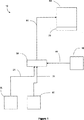
図1を参照すると、本発明の一実施の形態に従ったメガソニック洗浄システム10が示されている。メガソニック洗浄システム10は、二酸化炭素(CO2)ガス発生源20と、窒素(N2)ガス発生源30と、洗浄液供給源40と、膜接触器(membrane contactor)50と、処理チャンバー60と、メガソニック・エネルギー発生源70とを備えている。メガソニック・エネルギー発生源70は処理チャンバー60の底部に連結されるように示されているけれども、処理チャンバー60内に支持された半導体ウエハー(不図示)にメガソニック・エネルギー発生源70がメガソニック・エネルギーを供給する間における、処理チャンバー60に対するメガソニック・エネルギー発生源70の特定の配置位置を本発明が限定するものではない。
Referring to FIG. 1, a
本発明の一実施の形態に従って半導体ウエハーを洗浄するためのメガソニック洗浄システム10を使用するに際し、洗浄液(脱イオン水やRCA溶液や希酸や希塩基や半水溶性の溶剤などの半導体溶液が通常使用される)が、まず、洗浄液供給源40から膜接触器50へ流路41を通って供給される。他の洗浄液が本発明で使用されることができる。他のRCA洗浄液も含まれるがこれに限定されるものではない。同時に、二酸化炭素ガスが二酸化炭素ガス発生源20から膜接触器50に流路21を通って供給され、窒素ガスが窒素ガス発生源30から膜接触器50に流路31を通って供給される。膜接触器50は二酸化炭素ガスや窒素ガスを洗浄液(cleaning liquid)中に溶解させて洗浄溶液(cleaning solution)を形成するように作用する。本発明は、洗浄液に二酸化炭素ガスと窒素ガスとを溶解させることについて詳細に説明されているけれども、本発明はそれに限定されないことに注意すべきである。ガスの1つは、好ましくは、窒素(N2)や酸素(O2)やヘリウム(He)やアルゴン(Ar)や他のもののような、良好なパーティクル除去を促進するタイプである。ガスのもう一方は、好ましくは、メガソニック・エネルギーの照射の影響に伴うダメージから半導体ウエハーを保護するタイプのものである。そのようなガスの好ましい例は二酸化炭素である。さらに、それらのガスは膜接触器を使って洗浄液中に溶解されるけれども、液中にガスを溶解する他の公知の方法や装置が使用されることができる。
When using the
二酸化炭素ガスや窒素ガスが洗浄液に溶解される間、前記膜接触器50においては、制御された温度や圧力のガス環境が維持される。その膜接触器50のガス環境における、二酸化炭素ガスや窒素ガスの温度や分圧は制御されるので、処理チャンバー60内のガス環境における他の方法よりも、前記膜接触器50において、さらに多くの二酸化炭素ガスや窒素ガスが前記洗浄液に溶けるだろう。したがって、前記洗浄液に溶けている二酸化炭素や窒素ガスの量は、前記膜接触器50におけるガス環境の温度及び分圧にとって飽和濃度か、それよりも下であるけれども、該洗浄液における二酸化炭素や窒素ガスの溶解量は処理チャンバー60内のガス環境の温度や分圧においては過飽和濃度よりも上になるだろう。
While the carbon dioxide gas or nitrogen gas is dissolved in the cleaning liquid, the
例えば、体積比が1:1の窒素と二酸化炭素のみを含む、膜接触器50のガス環境、並びに、空気だけを含む処理チャンバー60のガス環境を考察する。両方のガス環境が大気圧で室温にあると仮定すれば、膜接触器50のガス環境における二酸化炭素の分圧は、前記処理チャンバー60のガス環境における二酸化炭素の分圧よりも大きくなるだろう。したがって、平衡状態で、膜接触器50のガス環境に曝されている洗浄液中の二酸化炭素の濃度は、処理チャンバー60のガス環境に曝されている洗浄液中の二酸化炭素の濃度よりも高いだろう。同じことは、溶解されている窒素ガスについても言える。
For example, consider the gas environment of the
所望の洗浄溶液を形成すべく所望量の二酸化炭素ガスや窒素ガスが洗浄液中に溶解された後、その洗浄溶液は流体路51を通って処理チャンバー60の中に導入される。処理チャンバー60に入れば、その洗浄溶液は、そこに支持されている1枚(又は複数枚)のウエハーと接触する。処理チャンバー60は好ましくは、大気圧及び室温にて空気を含む。したがって、その洗浄溶液が処理チャンバー60に到達したとき、洗浄溶液に溶解されている1又はそれ以上のガス(例えば、二酸化炭素ガスや窒素ガス)が飽和濃度を軽く超えるだろう。したがって、処理チャンバー60のガス環境の温度や分圧で飽和濃度よりも上になっている溶解ガスは、洗浄溶液から逃散する傾向となる。しかしながら、相当量のガスが洗浄溶液から逃散して、該洗浄溶液におけるガスの量が飽和濃度に戻るまでに、なるべくなら、(後述するような)処理/洗浄を完了させる。
After a desired amount of carbon dioxide gas or nitrogen gas is dissolved in the cleaning liquid to form a desired cleaning solution, the cleaning solution is introduced into the
好ましい実施の形態においては、洗浄溶液における二酸化炭素濃度は1000ppmであり、大気圧及び室温の空気中における二酸化炭素飽和濃度の1000倍以上である。二酸化炭素のこの濃度は、与えられたメガソニック・エネルギーと併せて使用された時、ウエハー・ダメージの無い、非常に効率的な洗浄を実現することが実験により明らかにされている。 In a preferred embodiment, the carbon dioxide concentration in the cleaning solution is 1000 ppm, which is at least 1000 times the carbon dioxide saturation concentration in air at atmospheric pressure and room temperature. Experiments have shown that this concentration of carbon dioxide provides very efficient cleaning without wafer damage when used in conjunction with a given megasonic energy.
前記洗浄溶液が処理チャンバー60に供給されて、該処理チャンバー60中の半導体ウエハー(1枚又は複数枚)と接触するとすぐに、メガソニック・エネルギー発生源70が作動される。使用される処理チャンバーのタイプに応じ、半導体ウエハーは洗浄溶液中に浸漬されるか、或いは、枚葉式処理チャンバーの場合には、前記洗浄溶液の層が前記ウエハーの表面に1層又はそれ以上供給されるかも知れない。本発明は処理チャンバーの特定のタイプに限定されるものではない。加えて、メガソニック・エネルギー発生源も、如何なる特有の形状、及び/又は位置付けに限定されない。例えば、メガソニック・エネルギー発生源はプレート状としても、細長いロッド状としても、三角形状としても、他の形状としても良い。本発明は、さらに、超音波の適用や、他の形式の音響エネルギーの適用と併せて使用されることができる。
As soon as the cleaning solution is supplied to the
駆動されると、メガソニック・エネルギー発生源70は、メガソニック・音響エネルギーを作り出す。該エネルギーは、前記洗浄溶液を通って、洗浄されるべき半導体ウエハー(1枚又は複数枚)にまで伝達される。洗浄溶液中に溶解された二酸化炭素(及び又は窒素)は、ウエハー表面に伝達されるメガソニック・エネルギーによるダメージから、洗浄されるウエハーを保護するように機能する。結果として、ポリシリコンや金属や誘電体を含む材料のラインやトレンチをエッチングした後に、繊細な特許請求の範囲のウエハーに、洗浄工程においてメガソニック・エネルギーを半導体ウエハーに供給することができる。
When driven, the
図4Aの図4Bとの比較が、洗浄溶液に溶解されるガスの1つである二酸化炭素の過飽和量の使用の有利さを示している。図4A及び図4Bは、顕微鏡を使用した、感度の良いビット線の構造のダメージの評価を示している。図中の暗い点はウエハーのダメージを示している。図4Aは、空気が飽和濃度である洗浄溶液を使用したことに伴うウエハー・ダメージを示している。洗浄効果は約99%であったが、ウエハーは深刻なダメージを受けた。図4Bは、本発明の一実施の形態に従ったもので、二酸化炭素が過飽和濃度である洗浄溶液を使用したことに伴うウエハー・ダメージを示している。洗浄効果はこの場合も約99%であったが、ウエハーはほとんどダメージを受けなかった。図4A及び図4Bに示されるようにウエハーを洗浄するために使用されるプロセスにおいて、メガソニック状態は等しく、溶解されたガスを除いて、洗浄溶液は等しかった。 Comparison of FIG. 4A with FIG. 4B shows the advantage of using a supersaturated amount of carbon dioxide, one of the gases dissolved in the cleaning solution. 4A and 4B show an evaluation of the damage of the sensitive bit line structure using a microscope. The dark dots in the figure indicate wafer damage. FIG. 4A shows the wafer damage associated with using a cleaning solution with a saturated concentration of air. Although the cleaning effect was about 99%, the wafer was severely damaged. FIG. 4B illustrates the wafer damage associated with using a supersaturated cleaning solution in accordance with one embodiment of the present invention. The cleaning effect was again about 99% in this case, but the wafer was hardly damaged. In the process used to clean the wafer as shown in FIGS. 4A and 4B, the megasonic state was equal and the cleaning solution was equal except for dissolved gas.
上述したように、本発明は、枚葉式処理チャンバーやバッチ処理チャンバー、或いは/及び浸漬又は非浸漬処理チャンバーを含む様々なタイプの処理チャンバーと共に実施されることができる。バッチタイプで浸漬式の処理タンクにも発明の本質が適用し得るという理解の下で、例として、枚葉式非浸漬タイプの処理チャンバーが検討される。 As mentioned above, the present invention can be implemented with various types of processing chambers, including single wafer processing chambers, batch processing chambers, and / or immersion or non-immersion processing chambers. With the understanding that the essence of the invention can also be applied to batch-type immersion processing tanks, a single wafer non-immersion processing chamber is considered as an example.
図2は、本発明に従って作成された枚葉非浸漬式のメガソニック・エネルギー洗浄装置101を示す。ウエハーの表面に薄い層を形成するため、図1との関係で説明したように、生成された洗浄溶液が、放出口214からウエハー106に供給される。もう一つの方法として、洗浄溶液は、ウエハー106の底面に供給されることもできる。放出口214は流体路51(図1参照)に連結されることもできる。該メガソニック・エネルギー洗浄装置101は、処理タンクの壁100に挿入された細長いプローブ104を有している。該処理タンクは、ウエハー106が本発明に従って処理される処理チャンバーを形成している。明示されるように、プローブ104は、一端がタンク101の外側に支持されている。プローブ104とタンク壁100との間に挟まれた、適切なOリング102が、処理タンク101の適切なシールを提供している。
FIG. 2 shows a single wafer non-immersion type megasonic energy cleaning apparatus 101 made in accordance with the present invention. In order to form a thin layer on the surface of the wafer, the generated cleaning solution is supplied to the
ハウジング120内に保持された熱伝導部材134は、プローブ104に音響的に且つ機械的に結合されている。また、ハウジング120内には、熱伝導部材134に音響的に結合された圧電変換器140が保持されている。分離片141及び電気コネクタ142、154、126が変換器140と音響エネルギー源(不図示)との間に接続されている。ハウジング120は、冷却剤のための注入導管124及び注出導管122を支持しており、電気コネクタ154及び126のための開口152を有している。該ハウジング120は、プローブ104のための開口132が形成された環状プレート118により閉塞されている。該プレート118は処理タンクに取り付けられている。該処理タンクの内部には、支持体又は受容器108がプローブ104に対して平行で近接するように配置されている。受容器108は、色々な形態をとることができる。図示した配置は、複数のスポーク108bによって支持された外縁部108aを有している。スポークは、軸110上に支持されたハブ108cに接続されており、該軸110は、処理タンクの底部壁を貫通して伸びている。タンク101の外部にて、軸110は、モータ112に接続されている。
A heat conducting member 134 held in the
細長いプローブ104は、音響エネルギーを効率的に伝える、石英のような比較的不活性な非汚染性材料で出来たものであることが好ましい。石英プローブを使用することは、殆どの洗浄溶液にとって満足し得るものであるが、フッ化水素酸を含む溶液は石英を食刻する可能性がある。このため、サファイア、炭化ケイ素、窒化ホウ素、ガラス質炭素、ガラス様炭素被覆黒鉛、又はその他の適宜な材料で出来たプローブを石英に代えて採用しても良い。また、炭化ケイ素又はガラス質炭素のような、HFに対して不活性な材料で石英を被覆してもよい。
The
プローブ104は、中実で細長くスピンドルやプローブのような洗浄部104aと、基部又は後ろ部104bとを有している。プローブ104の断面は円形であり、好ましくは、該洗浄部104aの直径は前記後ろ部104bの直径よりも小さい。好ましい実施の形態においては、後ろ部104bの後ろ面の面積は、洗浄部104aの先端面の面積の25倍である。もちろん、円形以外の断面形状を採用しても良い。小径の円柱状ロッド又は洗浄部104aは、プローブ104aに沿ってメガソニック・エネルギーを集中させる上で望ましい。しかしながら、プローブ104aの直径は、該プローブの伝えるメガソニック・エネルギーにより作り出される機械的振動に十分耐えるべきである。望ましくは、プローブ104aの直径は、加えられるエネルギーの周波数の波長に等しいか、該波長よりも小さくすべきである。この構造は、プローブに接触する液体の中にエネルギーを半径方向に導く、所望の定常表面波を生じさせる。要するに、ロッドの直径は、ロッドの長さに沿った、隔たった位置にて僅かに拡張し且つ、収縮する。好ましい実施の形態においては、ロッド104aの半径は、約0.2インチであり、約0.28インチの波長で発生させる。この形態はプローブの長さに沿ってインチ当たり3から4の波長を発生させる。
The
プローブの洗浄部104aは、ウェハの洗浄中、ウェハ106の全表面積がプローブ104に対して露呈されるように十分に長くすることが好ましい。1つの好ましい実施の形態において、ウェハ106は、プローブ104の下方にて回転するため、洗浄部104aは、少なくともウェハ106の中心に達するように十分に長いことが好ましい。その結果、ウェハ106がプローブ104の下方にて回転されるとき、ウェハ106の全表面積は、プローブ104の下方を通過することになる。プローブ先端からのメガソニック振動は、ウェハの中心に向けて多少の撹拌をもたらすであろうから、プローブ104は、ウェハ106の中心に達しない場合でさえ、多分、満足し得るように機能することができよう。プローブ104の長さは、所望の波長によっても決まる。通常、プローブの長さは、プローブ104に印加されるエネルギーの半波長の増分量にて変化する。好ましくは、プローブの洗浄部104aは、供給されるエネルギーのインチ当たり3から4の波長を含む。この実施の形態において、プローブの洗浄部104aのインチでの長さは、所望の波長を3から4の数で割ったものに等しい。変換器内の変数を要因として、変換器がその最も効果的な点にて機能するように、所望の波長が得られるように変換器140を調整することが必要である。
It is preferable that the probe cleaning unit 104 a is sufficiently long so that the entire surface area of the
タンク101の外部に配置されたプローブの後側部分104bは、洗浄部104aの直径よりも大きい直径となるように拡がっている。図2から図3に示した実施の形態において、プローブの後側部分の直径は、漸進的に、円筒状部分104dまで増大する。後側部分104dの端面の大きい表面積は、多量のメガソニック・エネルギーを伝導し、その後に、そのエネルギーが小径の洗浄部104a内に集中されるようにするために好ましい。 The rear portion 104b of the probe arranged outside the tank 101 is expanded so as to have a diameter larger than the diameter of the cleaning unit 104a. In the embodiment shown in FIGS. 2 to 3, the diameter of the rear portion of the probe gradually increases to the cylindrical portion 104d. The large surface area of the end face of the rear portion 104d is preferable for conducting a large amount of megasonic energy and then concentrating the energy in the small diameter cleaning section 104a.
使用時、プローブ104が音響的に作動している間、ノズル214からウエハの上面に洗浄溶液(図1に関して、上記で説明したように作られたもの)が噴霧される。洗浄溶液をノズルからウェハ106に噴霧することに代わるものとして、タンク101が洗浄溶液にて充填されるようにしても良い。その噴霧式の方法の場合、液体はプローブ104の下側部分と回転するウェハ106の隣接する上面との間にメニスカス216を形成する。そのメニスカス216はプローブの断面の下側部分を湿らせる。断面の湿った部分により画成される円弧の寸法は、洗浄溶液中で使用される液体の性質、プローブ104を製造するために使用される材料、ウェハ106とプローブ104の下縁部との間の垂直距離に伴って変化する。
In use, while the
前記洗浄溶液は、パーティクルを遊離させるために前記プローブ104内のメガソニック・エネルギーを前記ウエハー表面に伝導せしめる媒質となっている。これらの遊離されたパーティクルは、連続的に流れる噴霧液及び回転するウェハ106によって洗い流される。液体の流れが中断されるとき、洗浄溶液がウエハ106から放り出される遠心力によってある程度の乾燥作用が得られる。もう一つの方法として、メガソニック・エネルギー発生源が配置される側とはウエハーの反対側に、本発明の洗浄溶液、或いは他の洗浄媒質を供給することができる。本実施の形態では、ウエハーの反対側をも洗浄する十分なパワーでメガソニック・エネルギーを供給することが好ましい。
The cleaning solution is a medium that conducts megasonic energy in the
上述したように、二酸化炭素ガスや窒素ガスの相当量が洗浄溶液から逃散して、該洗浄溶液中のこれらのガスの量が飽和濃度に戻るまでに、メガソニック・エネルギーを与えることによるウエハーの処理/洗浄が完了される。該洗浄溶液中に飽和濃度で溶解された二酸化炭素(及び又は窒素)は、洗浄されるウエハーを、該ウエハーの表面に伝達されるメガソニック・エネルギーに伴うダメージから保護するために機能する。全ての機能は、完全にプログラムされたプロセッサ或いはコントローラにより達成される。 As noted above, wafers by applying megasonic energy before a significant amount of carbon dioxide gas or nitrogen gas escapes from the cleaning solution and the amount of these gases in the cleaning solution returns to saturation. Processing / cleaning is completed. Carbon dioxide (and / or nitrogen) dissolved at a saturating concentration in the cleaning solution serves to protect the wafer being cleaned from damage associated with megasonic energy transferred to the surface of the wafer. All functions are accomplished by a fully programmed processor or controller.
本発明は、当業者が簡単にそれを製造できると共に使用できるように、十分に詳しく説明され図示されているけれども、様々な代案や修正や改良が本発明の精神及び範囲から逸脱すること無しに容易に明白にされるべきである。具体的には、本発明は、洗浄液への2つのガスの導入に限定されるものではなく、処理チャンバーの環境にて過飽和濃度となるように、洗浄液にたった1つのガスが溶かされている場合も包含する。さらには、付加したガスが洗浄液に存在し、及び/又は、洗浄液が液体の混合物であることも可能である。 Although the present invention has been described and illustrated in sufficient detail to enable those skilled in the art to easily make and use it, various alternatives, modifications, and improvements may be made without departing from the spirit and scope of the invention. Should be easily clarified. Specifically, the present invention is not limited to the introduction of two gases into the cleaning liquid, but when only one gas is dissolved in the cleaning liquid so as to have a supersaturated concentration in the environment of the processing chamber. Is also included. Furthermore, it is possible that the added gas is present in the cleaning liquid and / or the cleaning liquid is a liquid mixture.
Claims (20)
(b) 音響エネルギー源を配置し、
(c) その基板の表面に溶液のフィルムを形成するように、洗浄液と、前記第1の温度及び前記第1の分圧で過飽和濃度となるように前記洗浄液に溶かされた第1のガスとを含む溶液を前記基板の表面に供給すると共に、該フィルムに前記音響エネルギー源を接触させ
(d) 前記基板が前記溶液と接触している間に該基板を洗浄すべく、前記音響エネルギー源によって前記溶液を介して該基板に音響エネルギーを供給する、
ことからなる、少なくとも1枚の基板を洗浄する方法。(a) placing a substrate in a processing chamber having a gas environment of a first temperature and a first partial pressure for a first gas;
(b) arrange an acoustic energy source;
( c ) a cleaning solution so as to form a film of the solution on the surface of the substrate, and a first gas dissolved in the cleaning solution so as to have a supersaturated concentration at the first temperature and the first partial pressure. the solution with the supplies to the surface of the substrate including contacting said acoustic energy source in the film
( d ) supplying acoustic energy to the substrate through the solution by the acoustic energy source to clean the substrate while the substrate is in contact with the solution;
A method for cleaning at least one substrate comprising:
は、前記ウエハーが、ポリシリコンや金属や誘電体を含む材料のラインやトレンチのエッチングを受けた後に実行される、請求項1の方法。The substrate is a semiconductor wafer, and steps (b)-( d )
The method of claim 1, wherein the wafer is performed after the wafer has undergone etching of lines or trenches of material comprising polysilicon, metal or dielectric.
前記溶液は、前記第1のガスの第2の温度及び第2の分圧を有するガス環境の中に前記洗浄液を供給し、前記第2の温度及び前記第2の分圧にて前記第1のガスが、飽和濃度か、それよりも下の濃度になるような量に、前記第1のガスを前記洗浄液に溶かすことによってステップ(c) の前に作り出され;
前記第1のガスは二酸化炭素であり;
前記溶液は、前記基板からパーティクルを除去することとなる、前記洗浄液に溶かされた第2のガスをさらに含み;
前記ステップ(b) ―(d) は、基板が金属ラインのエッチステップを受けた後に実行され、
前記処理チャンバーのガス環境は空気を含み;
該処理チャンバー内のガス環境の圧力は大気圧かそれに近い、
請求項1の方法。Step ( d ) is completed before the concentration of the first gas in the solution drops to a saturation concentration at the first temperature and the first partial pressure;
The solution supplies the cleaning liquid into a gas environment having a second temperature and a second partial pressure of the first gas, and the first solution at the second temperature and the second partial pressure. Is produced prior to step (c) by dissolving the first gas in the cleaning solution in an amount such that the gas is at a saturation concentration or below.
The first gas is carbon dioxide;
The solution further includes a second gas dissolved in the cleaning liquid that will remove particles from the substrate;
Steps (b)-( d ) are performed after the substrate has undergone a metal line etch step,
The gas environment of the processing chamber includes air;
The pressure of the gas environment in the processing chamber is at or near atmospheric pressure,
The method of claim 1.
前記ステップ(b) では、前記基板にごく接近するように前記プローブを配置し、In step (b), the probe is placed in close proximity to the substrate,
前記ステップ(c) では、前記溶液のフィルムが前記プローブと接触する、In step (c), the solution film contacts the probe;
請求項1の方法。The method of claim 1.
請求項18の方法。 In step (b), the probe is placed in close proximity to and parallel to the surface of the substrate;
The method of claim 18.
Applications Claiming Priority (2)
| Application Number | Priority Date | Filing Date | Title |
|---|---|---|---|
| US47760203P | 2003-06-11 | 2003-06-11 | |
| PCT/US2004/018464 WO2005006396A2 (en) | 2003-06-11 | 2004-06-10 | Megasonic cleaning using supersaturated cleaning solution |
Publications (3)
| Publication Number | Publication Date |
|---|---|
| JP2007502032A JP2007502032A (en) | 2007-02-01 |
| JP2007502032A5 JP2007502032A5 (en) | 2007-08-02 |
| JP4643582B2 true JP4643582B2 (en) | 2011-03-02 |
Family
ID=34061915
Family Applications (1)
| Application Number | Title | Priority Date | Filing Date |
|---|---|---|---|
| JP2006533684A Expired - Fee Related JP4643582B2 (en) | 2003-06-11 | 2004-06-10 | Megasonic cleaning using supersaturated cleaning solution |
Country Status (6)
| Country | Link |
|---|---|
| EP (1) | EP1631396A4 (en) |
| JP (1) | JP4643582B2 (en) |
| KR (1) | KR101110905B1 (en) |
| CN (1) | CN1849182A (en) |
| TW (1) | TWI330552B (en) |
| WO (1) | WO2005006396A2 (en) |
Families Citing this family (12)
| Publication number | Priority date | Publication date | Assignee | Title |
|---|---|---|---|---|
| KR20010108641A (en) * | 2000-05-30 | 2001-12-08 | 강병근 | Healthy beverage with radish and manufacturing method thereof |
| KR20020037177A (en) * | 2000-11-13 | 2002-05-18 | 김용현 | Honey drink added radish |
| KR100827618B1 (en) * | 2006-05-11 | 2008-05-07 | 한국기계연구원 | Ultrasonic device for cleaning and ultrasonic cleaning system using the same |
| US7969548B2 (en) * | 2006-05-22 | 2011-06-28 | Asml Netherlands B.V. | Lithographic apparatus and lithographic apparatus cleaning method |
| WO2008050832A1 (en) * | 2006-10-27 | 2008-05-02 | Tokyo Electron Limited | Substrate cleaning apparatus, substrate cleaning method, program and recording medium |
| KR100748480B1 (en) * | 2007-06-27 | 2007-08-10 | 한국기계연구원 | Ultrasonic device for cleaning and ultrasonic cleaning system using the same |
| JP4532580B2 (en) * | 2008-08-20 | 2010-08-25 | 株式会社カイジョー | Ultrasonic cleaning equipment |
| JP4915455B2 (en) * | 2010-02-25 | 2012-04-11 | トヨタ自動車株式会社 | Degreasing system using microbubbles for large products such as vehicles |
| JP2014130881A (en) * | 2012-12-28 | 2014-07-10 | Ebara Corp | Polishing device |
| JP6678448B2 (en) * | 2015-12-22 | 2020-04-08 | 株式会社Screenホールディングス | Substrate cleaning method and substrate cleaning apparatus |
| WO2020095091A1 (en) * | 2018-11-06 | 2020-05-14 | Arcelormittal | Equipment improving the ultrasound cleaning |
| JP7233691B2 (en) * | 2019-03-28 | 2023-03-07 | 株式会社エアレックス | Decontamination method for low-temperature goods and pass box used for this |
Family Cites Families (10)
| Publication number | Priority date | Publication date | Assignee | Title |
|---|---|---|---|---|
| US5368054A (en) | 1993-12-17 | 1994-11-29 | International Business Machines Corporation | Ultrasonic jet semiconductor wafer cleaning apparatus |
| JPH1022246A (en) | 1996-07-04 | 1998-01-23 | Tadahiro Omi | Cleaning method |
| WO1998008248A1 (en) * | 1996-08-20 | 1998-02-26 | Organo Corporation | Method and device for washing electronic parts member, or the like |
| US5800626A (en) | 1997-02-18 | 1998-09-01 | International Business Machines Corporation | Control of gas content in process liquids for improved megasonic cleaning of semiconductor wafers and microelectronics substrates |
| US5849091A (en) * | 1997-06-02 | 1998-12-15 | Micron Technology, Inc. | Megasonic cleaning methods and apparatus |
| US6167891B1 (en) | 1999-05-25 | 2001-01-02 | Infineon Technologies North America Corp. | Temperature controlled degassification of deionized water for megasonic cleaning of semiconductor wafers |
| JP3322853B2 (en) | 1999-08-10 | 2002-09-09 | 株式会社プレテック | Substrate drying device and cleaning device, and drying method and cleaning method |
| US6743301B2 (en) | 1999-12-24 | 2004-06-01 | mFSI Ltd. | Substrate treatment process and apparatus |
| US6684890B2 (en) * | 2001-07-16 | 2004-02-03 | Verteq, Inc. | Megasonic cleaner probe system with gasified fluid |
| US20030084916A1 (en) * | 2001-10-18 | 2003-05-08 | Sonia Gaaloul | Ultrasonic cleaning products comprising cleaning composition having dissolved gas |
-
2004
- 2004-06-10 JP JP2006533684A patent/JP4643582B2/en not_active Expired - Fee Related
- 2004-06-10 KR KR1020057023902A patent/KR101110905B1/en active IP Right Grant
- 2004-06-10 EP EP04776442.8A patent/EP1631396A4/en not_active Withdrawn
- 2004-06-10 WO PCT/US2004/018464 patent/WO2005006396A2/en not_active Application Discontinuation
- 2004-06-10 CN CNA2004800205237A patent/CN1849182A/en active Pending
- 2004-06-11 TW TW093116958A patent/TWI330552B/en active
Also Published As
| Publication number | Publication date |
|---|---|
| TWI330552B (en) | 2010-09-21 |
| EP1631396A4 (en) | 2013-08-14 |
| KR20060037270A (en) | 2006-05-03 |
| CN1849182A (en) | 2006-10-18 |
| WO2005006396A2 (en) | 2005-01-20 |
| EP1631396A2 (en) | 2006-03-08 |
| JP2007502032A (en) | 2007-02-01 |
| WO2005006396A3 (en) | 2005-09-15 |
| TW200507954A (en) | 2005-03-01 |
| KR101110905B1 (en) | 2012-02-20 |
Similar Documents
| Publication | Publication Date | Title |
|---|---|---|
| US7578302B2 (en) | Megasonic cleaning using supersaturated solution | |
| US7021319B2 (en) | Assisted rinsing in a single wafer cleaning process | |
| JP4643582B2 (en) | Megasonic cleaning using supersaturated cleaning solution | |
| KR100385255B1 (en) | Method of cleaning porous body, and process for producing porous body, non-porous film or bonded substrate | |
| US8960208B2 (en) | Ultrasonic cleaning device | |
| US20010032657A1 (en) | Megasonic treatment apparatus | |
| WO2008008921A2 (en) | Tranducer assembly incorporating a transmitter having through holes, and method of cleaning | |
| US7682457B2 (en) | Frontside structure damage protected megasonics clean | |
| JP2004515053A (en) | Wafer cleaning method and apparatus | |
| KR100473475B1 (en) | Apparatus for cleaning a substrate | |
| US20090235952A1 (en) | Device and method for wet treating plate-like substrates | |
| JPH11260778A (en) | Sheet style surface cleaning method and equipment | |
| KR20040102588A (en) | Apparatus and Method For Cleaning Wafer | |
| JP2007502032A5 (en) | ||
| JP2003031548A (en) | Method for treating surface of substrate | |
| JP2010082621A (en) | Ultrasonic cleaning apparatus | |
| US20210233782A1 (en) | Methods and apparatus for cleaning semiconductor wafers | |
| KR100694798B1 (en) | Method for cleaning the subsrtrate | |
| TWI528436B (en) | Acoustic energy system, method and apparatus for processing flat articles | |
| KR100954566B1 (en) | Transmitter and wafer cleaning apparatus compring the same | |
| KR20090125484A (en) | Apparatus and method for cleaning substrate | |
| KR20090093627A (en) | Apparatus and method for cleaning substrate |
Legal Events
| Date | Code | Title | Description |
|---|---|---|---|
| A711 | Notification of change in applicant |
Free format text: JAPANESE INTERMEDIATE CODE: A711 Effective date: 20061211 |
|
| A521 | Written amendment |
Free format text: JAPANESE INTERMEDIATE CODE: A821 Effective date: 20061211 |
|
| A521 | Written amendment |
Free format text: JAPANESE INTERMEDIATE CODE: A523 Effective date: 20070601 |
|
| A621 | Written request for application examination |
Free format text: JAPANESE INTERMEDIATE CODE: A621 Effective date: 20070601 |
|
| A131 | Notification of reasons for refusal |
Free format text: JAPANESE INTERMEDIATE CODE: A131 Effective date: 20090929 |
|
| A601 | Written request for extension of time |
Free format text: JAPANESE INTERMEDIATE CODE: A601 Effective date: 20091224 |
|
| A602 | Written permission of extension of time |
Free format text: JAPANESE INTERMEDIATE CODE: A602 Effective date: 20100106 |
|
| A601 | Written request for extension of time |
Free format text: JAPANESE INTERMEDIATE CODE: A601 Effective date: 20100203 |
|
| A521 | Written amendment |
Free format text: JAPANESE INTERMEDIATE CODE: A523 Effective date: 20100205 |
|
| A072 | Dismissal of procedure [no reply to invitation to correct request for examination] |
Free format text: JAPANESE INTERMEDIATE CODE: A072 Effective date: 20100615 |
|
| A131 | Notification of reasons for refusal |
Free format text: JAPANESE INTERMEDIATE CODE: A131 Effective date: 20100706 |
|
| A521 | Written amendment |
Free format text: JAPANESE INTERMEDIATE CODE: A523 Effective date: 20101005 |
|
| TRDD | Decision of grant or rejection written | ||
| A01 | Written decision to grant a patent or to grant a registration (utility model) |
Free format text: JAPANESE INTERMEDIATE CODE: A01 Effective date: 20101102 |
|
| A01 | Written decision to grant a patent or to grant a registration (utility model) |
Free format text: JAPANESE INTERMEDIATE CODE: A01 |
|
| A61 | First payment of annual fees (during grant procedure) |
Free format text: JAPANESE INTERMEDIATE CODE: A61 Effective date: 20101202 |
|
| R150 | Certificate of patent or registration of utility model |
Ref document number: 4643582 Country of ref document: JP Free format text: JAPANESE INTERMEDIATE CODE: R150 Free format text: JAPANESE INTERMEDIATE CODE: R150 |
|
| FPAY | Renewal fee payment (event date is renewal date of database) |
Free format text: PAYMENT UNTIL: 20131210 Year of fee payment: 3 |
|
| R250 | Receipt of annual fees |
Free format text: JAPANESE INTERMEDIATE CODE: R250 |
|
| R250 | Receipt of annual fees |
Free format text: JAPANESE INTERMEDIATE CODE: R250 |
|
| R250 | Receipt of annual fees |
Free format text: JAPANESE INTERMEDIATE CODE: R250 |
|
| R250 | Receipt of annual fees |
Free format text: JAPANESE INTERMEDIATE CODE: R250 |
|
| R250 | Receipt of annual fees |
Free format text: JAPANESE INTERMEDIATE CODE: R250 |
|
| S111 | Request for change of ownership or part of ownership |
Free format text: JAPANESE INTERMEDIATE CODE: R313113 |
|
| R350 | Written notification of registration of transfer |
Free format text: JAPANESE INTERMEDIATE CODE: R350 |
|
| R250 | Receipt of annual fees |
Free format text: JAPANESE INTERMEDIATE CODE: R250 |
|
| R250 | Receipt of annual fees |
Free format text: JAPANESE INTERMEDIATE CODE: R250 |
|
| LAPS | Cancellation because of no payment of annual fees |