JP4641124B2 - Multiple coupled inverter device - Google Patents
Multiple coupled inverter device Download PDFInfo
- Publication number
- JP4641124B2 JP4641124B2 JP2001235384A JP2001235384A JP4641124B2 JP 4641124 B2 JP4641124 B2 JP 4641124B2 JP 2001235384 A JP2001235384 A JP 2001235384A JP 2001235384 A JP2001235384 A JP 2001235384A JP 4641124 B2 JP4641124 B2 JP 4641124B2
- Authority
- JP
- Japan
- Prior art keywords
- output
- inverter
- pwm
- carrier signal
- master
- Prior art date
- Legal status (The legal status is an assumption and is not a legal conclusion. Google has not performed a legal analysis and makes no representation as to the accuracy of the status listed.)
- Expired - Fee Related
Links
Images


Classifications
-
- H—ELECTRICITY
- H02—GENERATION; CONVERSION OR DISTRIBUTION OF ELECTRIC POWER
- H02M—APPARATUS FOR CONVERSION BETWEEN AC AND AC, BETWEEN AC AND DC, OR BETWEEN DC AND DC, AND FOR USE WITH MAINS OR SIMILAR POWER SUPPLY SYSTEMS; CONVERSION OF DC OR AC INPUT POWER INTO SURGE OUTPUT POWER; CONTROL OR REGULATION THEREOF
- H02M7/00—Conversion of ac power input into dc power output; Conversion of dc power input into ac power output
- H02M7/42—Conversion of dc power input into ac power output without possibility of reversal
- H02M7/44—Conversion of dc power input into ac power output without possibility of reversal by static converters
- H02M7/48—Conversion of dc power input into ac power output without possibility of reversal by static converters using discharge tubes with control electrode or semiconductor devices with control electrode
- H02M7/483—Converters with outputs that each can have more than two voltages levels
- H02M7/49—Combination of the output voltage waveforms of a plurality of converters
-
- H—ELECTRICITY
- H02—GENERATION; CONVERSION OR DISTRIBUTION OF ELECTRIC POWER
- H02M—APPARATUS FOR CONVERSION BETWEEN AC AND AC, BETWEEN AC AND DC, OR BETWEEN DC AND DC, AND FOR USE WITH MAINS OR SIMILAR POWER SUPPLY SYSTEMS; CONVERSION OF DC OR AC INPUT POWER INTO SURGE OUTPUT POWER; CONTROL OR REGULATION THEREOF
- H02M7/00—Conversion of ac power input into dc power output; Conversion of dc power input into ac power output
- H02M7/42—Conversion of dc power input into ac power output without possibility of reversal
- H02M7/44—Conversion of dc power input into ac power output without possibility of reversal by static converters
- H02M7/48—Conversion of dc power input into ac power output without possibility of reversal by static converters using discharge tubes with control electrode or semiconductor devices with control electrode
- H02M7/493—Conversion of dc power input into ac power output without possibility of reversal by static converters using discharge tubes with control electrode or semiconductor devices with control electrode the static converters being arranged for operation in parallel
-
- H—ELECTRICITY
- H02—GENERATION; CONVERSION OR DISTRIBUTION OF ELECTRIC POWER
- H02M—APPARATUS FOR CONVERSION BETWEEN AC AND AC, BETWEEN AC AND DC, OR BETWEEN DC AND DC, AND FOR USE WITH MAINS OR SIMILAR POWER SUPPLY SYSTEMS; CONVERSION OF DC OR AC INPUT POWER INTO SURGE OUTPUT POWER; CONTROL OR REGULATION THEREOF
- H02M1/00—Details of apparatus for conversion
- H02M1/0067—Converter structures employing plural converter units, other than for parallel operation of the units on a single load
- H02M1/0077—Plural converter units whose outputs are connected in series
Landscapes
- Engineering & Computer Science (AREA)
- Power Engineering (AREA)
- Inverter Devices (AREA)
- Supply And Distribution Of Alternating Current (AREA)
Description
【0001】
【発明の属する技術分野】
本発明は、複数のPWMインバータを多重化して構成される多重結合インバータ装置に係り、特に、各交流出力に含まれるキャリア信号が同相で重畳されることにより生じる電流リップルを低減させた多重結合インバータ装置に関する。
【0002】
【従来の技術】
PWMインバータ装置は、交流発電機や交流電源からの交流電力を直流電力に変換するコンバータ部と、このコンバータ部からの直流電力を任意の周波数を有する交流電力に再変換するインバータ部とから構成されている。インバータ部は、電圧指令や周波数指令等の波形指令とキャリア信号とに基づいて生成されるPWM信号によって、インバータ部を構成するスイッチング素子(例えばパワートランジスタ)をPWM制御することにより、任意の周波数を有する交流電力を出力する。このようなPWMインバータを多重結合することで高電圧出力を得る技術が、例えば特開昭60−98875号公報に開示されている。
【0003】
【発明が解決しようとする課題】
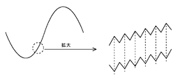
PWM信号で制御されるPWMインバータの交流出力には、図8に示したように、前記PWM信号の生成に用いられたキャリア信号成分が含まれる。したがって、各交流出力を、そのキャリア信号成分が同相となるように重畳してしまうと、図9に示したように、前記キャリア信号成分が実質的に増幅されてしまい、交流出力の電圧リップルが大きくなってしまうという技術課題があった。
【0004】
本発明の目的は、上記した従来技術の課題を解決し、多重化されたPWMインバータから出力される各交流出力に含まれるキャリア信号成分が同相で重畳されることにより生じる電流リップルを低減させることにある。
【0005】
【課題を解決するための手段】
要求出力の波形指令とキャリア信号とに基づいて生成されるPWM信号で制御される2系統のPWMインバータを多重化し、各PWMインバータの交流出力を相互に重畳する多重結合インバータ装置において、各PWMインバータの交流出力を、この交流出力に含まれるキャリア信号成分が相互に逆位相となるように重畳したことを特徴とする。
【0006】
上記した特徴によれば、各PWMインバータの交流出力を相互に重畳すると、そのキャリア信号成分が相互に相殺されるので、電流リップルを低減させることができる。
【0007】
【発明の実施の形態】
以下、図面を参照して本発明を詳細に説明する。図1は、本発明の一実施形態であるエンジン発電機の多重化インバータ装置の主要部の構成を示したブロック図である。
【0008】
発電機2は、2系統の3相メイン巻線2A,2Bを備え、エンジン1により駆動される。エンジン1の出力は、ステップモータ5により開度調整されるスロットル(図示せず)によって制御される。メイン巻線2A,2Bの出力段には、インバータ回路3a(マスタ),3b(スレーブ)がそれぞれ接続されている。マスタ3aおよびスレーブ3bの出力段は直列・並列切換部4に接続されている。前記直列・並列切換部4は、マスタ3aおよびスレーブ3bの各交流出力を、直列または並列に接続して両者を重畳する。
【0009】
前記3相メイン巻線2Bの出力段にはトランス7の一次コイル71が接続されている。トランス7の二次側には3つのサブコイル72(72a,72b,72c)が二次コイルとして結合されている。
【0010】
サブコイル72a,72bはインバータ電源コイルであり、それぞれマスタ3aの制御電源34aおよびスレーブ3bの制御電源34bへ駆動電力を供給する。サブコイル72cは、内部バッテリ(図示せず)へ充電電流を供給するための充電コイル、または直流電圧を外部ソケット(図示せず)へ供給するための外部直流電源コイルである。
【0011】
このように、本実施形態では発電機2の出力の一部をトランス7を介して取り出し、インバータ電源やバッテリ充電電源等の内部電源として利用するので、内部電源として必要な電力に応じてトランス7の一次コイル71と二次コイル72との巻数比を設定すれば、発電機2のメイン出力から必要な電力のみを取り出すことができ、発電効率を向上させることができる。
【0012】
さらに、本実施形態ではトランス7の二次側を複数のサブコイル72a,72b,72cで構成したので、内部電源で駆動される複数の電気負荷における消費電力に応じて各サブコイルの巻数を設定すれば、交流発電機のメイン出力から内部電源として必要な電力を正確に取り出せるようになる。
【0013】
マスタ3aにおいて、3相メイン巻線2Aの出力は、整流平滑回路31a、インバータ回路32aおよびフィルタ回路33aを経由して前記直列・並列切換部4へ供給される。前記整流平滑回路31aは、サイリスタブリッジ回路311aおよび平滑回路312aから構成される。前記インバータ回路32aは、電界効果トランジスタ(FET)ブリッジ321aおよび平滑回路322aから構成される。
【0014】
SCRドライバ37aは、サイリスタブリッジ回路311aを構成するサイリスタの導通角を制御する。回転検出部35aは、前記制御電極34aの交流出力に基づいてエンジン回転数を検知する。ガバナ制御部36aは、前記検知されたエンジン回転数に基づいて、前記ステップモータ5を制御する。インバータ制御部38aは、要求出力に応じたPWM信号をインバータ回路32aへ供給する。
【0015】
なお、スレーブ3bの構成は、前記回転検出部35aおよびガバナ制御部36aを搭載していない点を除いて前記マスタ3aと同等なので、その説明は省略する。また、各インバータ回路3a,3b間は通信線8で接続されており、互いを同期運転するための制御信号および同期信号が、この通信線8を介して送受される。
【0016】
図2は、前記マスタ3aおよびスレーブ3bに搭載されるインバータ制御部38a、38bの構成を示したブロック図である。
【0017】
インバータ制御部38aにおいて、キャリア信号発生部381aは、キャリア信号としての三角波を出力する。正弦波発生部382aは、電圧指令、周波数指令および位相指令等の波形指令に基づいて正弦波を出力する。比較部383aは、前記キャリア信号および正弦波の比較結果に基づいてPWM信号を生成し、これを出力する。このPWM信号は、FETブリッジ321aを構成する各EFTのゲートに印加される。
【0018】
なお、インバータ制御部38bの構成は、上記したインバータ制御部38aの構成と同等なので、その説明は省略する。但し、各インバータ回路3a,3b間は前記通信線8を介して同期信号を送受し、それぞれの正弦波発生部382a、382bに供給される位相指令は、出力正弦波が逆相すなわち位相が180°ずれるように調整されている。
【0019】
上記した構成によれば、マスタ3aおよびスレーブ3bの各インバータ回路3a,3bから出力される交流電圧Va、Vbは、位相が相互に逆相であって、これに含まれるキャリア信号成分が同相となる。
【0020】
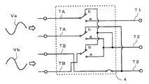
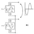
続いて、前記2つのインバータ回路の直列・並列接続切り換えについて説明する。図3は、前記直列・並列切換部4の詳細を示した回路図であり、図4,5は、その機能を模式的に表現した図である。
【0021】
本実施形態では、マスタ3aおよびスレーブ3bの交流出力Va、Vbを直列接続する際は、図4に示したように、スレーブ3bの交流出力Vbを反転したうえでマスタ3aの交流出力Vaに対して直列的に重畳する。各交流出力Va、Vbを並列接続する際は、図5に示したように、スレーブ3bの交流出力Vbを反転したうえでマスタ3aの交流出力Vaに対して並列的に重畳する。
【0022】
これにより、交流電圧Va、Vbは同位相で重畳されるのに対して、そのキャリア信号成分は、図6に示したように逆位相で重畳されて相殺される。この結果、直列・並列切換部4からは、図7に示したように、電圧リップルが低減された交流出力を得られるようになる。
【0023】
前記直列・並列切換部4はトグルスイッチで構成することができ、スイッチが接点a側に切り換えられているときは、出力端子T1およびT2間には、マスタ3aの出力電圧Vaが出力され、出力端子T2およびT3間にはスレーブ3bの出力電圧Vbが逆相が出力され、結果的に出力端子T1およびT3間ではマスタ3aおよびスレーブ3bの出力電圧の2倍の出力電圧が得られる。すなわち、マスタ3aとスレーブ3bとは直列に接続されたことになる。
【0024】
また、スイッチが接点b側に切り換えられているときは、出力端子T1およびT2間には電圧が出力されず、出力端子T2およびT3間にのみ、マスタ3aおよびスレーブ3bによる出力電圧が出力される。結果的に出力端子T2およびT3間には、マスタ3a,スレーブ3bのそれぞれの出力電圧が変化されずに、その出力が2倍になって現れる。すなわち、マスタ3aとスレーブ3bとは並列に接続されたことになる。
【0025】
このように、本実施形態によれば、マスタ3aおよびスレーブ3bの各交流出力Va、Vbは同位相で重畳されるのに対して、そのキャリア信号成分は逆相で重畳されるので相殺される。したがって、電圧リップルの少ない交流出力を得られるようになる。
【0026】
【発明の効果】
本発明によれば、2つの系統から出力される交流出力同士を、そのキャリア信号成分が相互に相殺されるように重畳されるので、電圧リップルの小さい交流出力を得られるようになる。
【図面の簡単な説明】
【図1】 本発明の一実施形態であるエンジン発電機の多重化インバータ装置の構成を示したブロック図である。
【図2】 インバータ制御部の構成を示したブロック図である。
【図3】 直列・並列切換部の回路図である。
【図4】 直列・並列切換部の直列接続機能を模式的に示した図である。
【図5】 直列・並列切換部の並列接続機能を模式的に示した図である。
【図6】 キャリア信号成分の相殺方法を示した図である。
【図7】 本発明の効果を説明するための図である。
【図8】 従来技術の問題点を示した図である。
【図9】 従来技術の問題点を示した図である。
【符号の説明】
1…エンジン、2…エンジン発電機、3a(マスタ)…インバータ回路、3b(スレーブ)…インバータ回路、4…直列・並列切換部、5…ステップモータ、7…トランス、31a,31b…整流平滑回路、32a,32b…インバータ回路、33a,33b…フィルタ回路、34a,34b…制御電源34a,34b…、35a…回転検出部、36a…ガバナ制御部、37a,37b…SCRドライバ、38…インバータ制御部、71…一次コイル、72(72a,72b,72c)…サブコイル[0001]
BACKGROUND OF THE INVENTION
The present invention relates to a multi-coupled inverter device configured by multiplexing a plurality of PWM inverters, and in particular, a multi-coupled inverter that reduces current ripple caused by superposition of carrier signals included in each AC output in the same phase. Relates to the device.
[0002]
[Prior art]
The PWM inverter device is composed of a converter unit that converts AC power from an AC generator or AC power source into DC power, and an inverter unit that reconverts DC power from the converter unit into AC power having an arbitrary frequency. ing. The inverter unit controls the switching element (for example, a power transistor) constituting the inverter unit by PWM control using a PWM signal generated based on a waveform command such as a voltage command or a frequency command and a carrier signal. The alternating current power which has is output. A technique for obtaining a high voltage output by multiple coupling of such PWM inverters is disclosed in, for example, Japanese Patent Laid-Open No. 60-98875.
[0003]
[Problems to be solved by the invention]
The AC output of the PWM inverter controlled by the PWM signal includes a carrier signal component used for generating the PWM signal, as shown in FIG. Therefore, if each AC output is superimposed so that the carrier signal component is in phase, the carrier signal component is substantially amplified as shown in FIG. 9, and the voltage ripple of the AC output is reduced. There was a technical problem of becoming larger.
[0004]
An object of the present invention is to solve the above-described problems of the prior art and reduce current ripple caused by superposition of carrier signal components included in each AC output output from a multiplexed PWM inverter in the same phase. It is in.
[0005]
[Means for Solving the Problems]
Each PWM inverter is a multi-coupled inverter that multiplexes two systems of PWM inverters controlled by PWM signals generated based on the required output waveform command and carrier signal, and superimposes the AC outputs of the PWM inverters. The AC output is superimposed so that carrier signal components contained in the AC output are in opposite phases.
[0006]
According to the above feature, when the AC outputs of the PWM inverters are superposed on each other, the carrier signal components cancel each other, so that the current ripple can be reduced.
[0007]
DETAILED DESCRIPTION OF THE INVENTION
Hereinafter, the present invention will be described in detail with reference to the drawings. FIG. 1 is a block diagram showing a configuration of a main part of a multiplex inverter device for an engine generator according to an embodiment of the present invention.
[0008]
The
[0009]
A
[0010]
The subcoils 72a and 72b are inverter power supply coils, and supply driving power to the control power supply 34a of the
[0011]
In this way, in this embodiment, a part of the output of the
[0012]
Furthermore, in the present embodiment, the secondary side of the
[0013]
In the
[0014]
The
[0015]
The configuration of the
[0016]
FIG. 2 is a block diagram showing a configuration of
[0017]
In the
[0018]
Note that the configuration of the
[0019]
According to the configuration described above, the AC voltages Va and Vb output from the
[0020]
Subsequently, switching between the series and parallel connection of the two inverter circuits will be described. FIG. 3 is a circuit diagram showing details of the series /
[0021]
In this embodiment, when the AC outputs Va and Vb of the
[0022]
As a result, the AC voltages Va and Vb are superimposed with the same phase, whereas the carrier signal components are superimposed with the opposite phase and canceled as shown in FIG. As a result, the AC output with reduced voltage ripple can be obtained from the series /
[0023]
The series /
[0024]
When the switch is switched to the contact b side, no voltage is output between the output terminals T1 and T2, and output voltages from the
[0025]
As described above, according to the present embodiment, the AC outputs Va and Vb of the
[0026]
【The invention's effect】
According to the present invention, the AC outputs output from the two systems are superimposed so that their carrier signal components cancel each other, so that an AC output with a small voltage ripple can be obtained.
[Brief description of the drawings]
FIG. 1 is a block diagram showing a configuration of a multiplexed inverter device for an engine generator according to an embodiment of the present invention.
FIG. 2 is a block diagram showing a configuration of an inverter control unit.
FIG. 3 is a circuit diagram of a series / parallel switching unit.
FIG. 4 is a diagram schematically illustrating a series connection function of a series / parallel switching unit.
FIG. 5 is a diagram schematically illustrating a parallel connection function of a series / parallel switching unit.
FIG. 6 is a diagram illustrating a carrier signal component canceling method.
FIG. 7 is a diagram for explaining the effect of the present invention.
FIG. 8 is a diagram showing a problem of a conventional technique.
FIG. 9 is a diagram showing a problem of the prior art.
[Explanation of symbols]
DESCRIPTION OF SYMBOLS 1 ... Engine, 2 ... Engine generator, 3a (master) ... Inverter circuit, 3b (slave) ... Inverter circuit, 4 ... Series / parallel switching part, 5 ... Step motor, 7 ... Transformer, 31a, 31b ...
Claims (1)
前記各PWMインバータの交流出力は相互に逆位相であって、そのキャリア信号成分は相互に同相であり、
前記各PWMインバータの交流出力を、そのキャリア信号成分が相互に逆位相となるように重畳する切換手段を具備し、
前記切換手段は、
一方のPWMインバータの正極と他方のPWMインバータの負極とを接続して出力端子の一方とし、一方のPWMインバータの負極と他方のPWMインバータの正極とを接続して出力端子の他方とする第1ポジションと、
各PWMインバータの負極同士を接続し、各正極を出力端子とする第2ポジションとを備えることを特徴とする多重結合インバータ装置。In a multiple coupled inverter device that multiplexes two systems of PWM inverters controlled by a PWM signal generated based on a waveform command of a required output and a carrier signal, and superimposes the AC outputs of the PWM inverters,
The AC outputs of the PWM inverters are opposite in phase to each other, and their carrier signal components are in phase with each other.
The AC output of each PWM inverter comprises switching means for superimposing so that the carrier signal components are in opposite phases to each other ,
The switching means is
The first positive terminal of one PWM inverter and the negative terminal of the other PWM inverter are connected as one of the output terminals, and the negative terminal of one PWM inverter and the positive terminal of the other PWM inverter are connected as the other output terminal. Position,
A multi-coupled inverter device comprising: a second position in which the negative electrodes of each PWM inverter are connected to each other and each positive electrode is used as an output terminal .
Priority Applications (2)
| Application Number | Priority Date | Filing Date | Title |
|---|---|---|---|
| JP2001235384A JP4641124B2 (en) | 2001-08-02 | 2001-08-02 | Multiple coupled inverter device |
| US10/161,594 US6813167B2 (en) | 2001-08-02 | 2002-06-05 | Multiplex connection inverter apparatus |
Applications Claiming Priority (1)
| Application Number | Priority Date | Filing Date | Title |
|---|---|---|---|
| JP2001235384A JP4641124B2 (en) | 2001-08-02 | 2001-08-02 | Multiple coupled inverter device |
Publications (2)
| Publication Number | Publication Date |
|---|---|
| JP2003047253A JP2003047253A (en) | 2003-02-14 |
| JP4641124B2 true JP4641124B2 (en) | 2011-03-02 |
Family
ID=19066840
Family Applications (1)
| Application Number | Title | Priority Date | Filing Date |
|---|---|---|---|
| JP2001235384A Expired - Fee Related JP4641124B2 (en) | 2001-08-02 | 2001-08-02 | Multiple coupled inverter device |
Country Status (2)
| Country | Link |
|---|---|
| US (1) | US6813167B2 (en) |
| JP (1) | JP4641124B2 (en) |
Families Citing this family (15)
| Publication number | Priority date | Publication date | Assignee | Title |
|---|---|---|---|---|
| JP4019979B2 (en) * | 2003-03-04 | 2007-12-12 | 富士電機ホールディングス株式会社 | AC-AC power converter |
| JP2005086918A (en) * | 2003-09-09 | 2005-03-31 | Fanuc Ltd | Motor driving device |
| US7425806B2 (en) * | 2004-04-12 | 2008-09-16 | York International Corporation | System and method for controlling a variable speed drive |
| JP4679891B2 (en) * | 2004-11-30 | 2011-05-11 | トヨタ自動車株式会社 | AC voltage generator and power output device |
| US7224147B2 (en) * | 2005-07-20 | 2007-05-29 | Hamilton Sundstrand Corporation | Buck/boost method of voltage regulation for a permanent magnet generator (PMG) |
| JP5395394B2 (en) * | 2008-10-09 | 2014-01-22 | 本田技研工業株式会社 | Generator series connection device |
| KR101094002B1 (en) * | 2009-12-16 | 2011-12-15 | 삼성에스디아이 주식회사 | Power converting device |
| KR101159023B1 (en) * | 2011-01-17 | 2012-06-21 | 엘에스산전 주식회사 | Method for sharing input and output port |
| CN103312187B (en) * | 2012-03-09 | 2016-02-03 | 台达电子工业股份有限公司 | A kind of converter system |
| EP2919382A4 (en) * | 2012-11-09 | 2016-09-14 | Honda Motor Co Ltd | Power source device |
| JP6809960B2 (en) * | 2017-03-30 | 2021-01-06 | 本田技研工業株式会社 | Generator system |
| JP6836445B2 (en) * | 2017-03-30 | 2021-03-03 | 本田技研工業株式会社 | Generator system |
| US10822116B2 (en) * | 2017-05-17 | 2020-11-03 | Ge Aviation Systems Llc | Power distribution network |
| CN109713911A (en) * | 2019-03-06 | 2019-05-03 | 重庆瑜欣平瑞电子股份有限公司 | The high-power twin voltage inverter circuit structure of general gasoline generator |
| CN116545282B (en) * | 2023-04-06 | 2024-03-19 | 山东艾诺智能仪器有限公司 | High-low gear switching method of high-frequency isolation alternating-current power supply and alternating-current power supply |
Citations (2)
| Publication number | Priority date | Publication date | Assignee | Title |
|---|---|---|---|---|
| JPH05137341A (en) * | 1991-11-15 | 1993-06-01 | Toshiba Corp | Method of reducing noise of electromagnetic equipment, and power converter |
| JPH08205535A (en) * | 1995-01-20 | 1996-08-09 | Takasago Seisakusho:Kk | Control method for voltage resonance dc to dc converter |
Family Cites Families (8)
| Publication number | Priority date | Publication date | Assignee | Title |
|---|---|---|---|---|
| JPH0815394B2 (en) | 1983-10-31 | 1996-02-14 | 株式会社安川電機 | Connection / control method of multiple coupling inverter device |
| JPS645358A (en) * | 1987-06-25 | 1989-01-10 | Mitsubishi Electric Corp | Elevator apparatus driven by inverter |
| US4814965A (en) * | 1987-09-30 | 1989-03-21 | Spectra Physics | High power flyback, variable output voltage, variable input voltage, decoupled power supply |
| JP2685586B2 (en) * | 1989-06-30 | 1997-12-03 | 株式会社日立製作所 | Multiple inverter device |
| JPH0678548A (en) | 1992-08-20 | 1994-03-18 | Nippon Electric Ind Co Ltd | Suppressing method for unbalanced direct current in multiple pwm inverter using interphase reactor |
| DE69521370T2 (en) * | 1994-03-02 | 2001-10-11 | Yaskawa Denki Kitakyushu Kk | MULTIPLE COUPLED POWER CONVERTER AND ITS CONTROL METHOD |
| US6281664B1 (en) * | 1999-01-13 | 2001-08-28 | Honda Giken Kogyo Kabushiki Kaisha | Generator and generator apparatus |
| US6411530B2 (en) * | 2000-04-06 | 2002-06-25 | Robicon Corporation | Drive and power supply with phase shifted carriers |
-
2001
- 2001-08-02 JP JP2001235384A patent/JP4641124B2/en not_active Expired - Fee Related
-
2002
- 2002-06-05 US US10/161,594 patent/US6813167B2/en not_active Expired - Lifetime
Patent Citations (2)
| Publication number | Priority date | Publication date | Assignee | Title |
|---|---|---|---|---|
| JPH05137341A (en) * | 1991-11-15 | 1993-06-01 | Toshiba Corp | Method of reducing noise of electromagnetic equipment, and power converter |
| JPH08205535A (en) * | 1995-01-20 | 1996-08-09 | Takasago Seisakusho:Kk | Control method for voltage resonance dc to dc converter |
Also Published As
| Publication number | Publication date |
|---|---|
| US6813167B2 (en) | 2004-11-02 |
| US20030025398A1 (en) | 2003-02-06 |
| JP2003047253A (en) | 2003-02-14 |
Similar Documents
| Publication | Publication Date | Title |
|---|---|---|
| JP4641124B2 (en) | Multiple coupled inverter device | |
| KR100437932B1 (en) | Multi-output power conversion circuit | |
| JP3578930B2 (en) | Generators and generator equipment | |
| JP2004282828A (en) | Bidirectional dc-dc converter | |
| JP2004080931A (en) | Starter generator for internal combustion engine | |
| EP2031749B1 (en) | On-vehicle rotary electric machine operating on two modes of rectification | |
| JP2004282826A (en) | Engine driven generator | |
| CN111095767B (en) | Driving power supply device | |
| US20170194887A1 (en) | Excitation device of ac exciter | |
| WO2007069314A1 (en) | Power converting apparatus | |
| JPH08256497A (en) | Motor drive method | |
| US5930134A (en) | Starting system for a prime mover | |
| JP4059083B2 (en) | Power converter | |
| JP2000358305A (en) | Power device for hybrid electric vehicle | |
| JP3584686B2 (en) | Voltage source power conversion circuit | |
| JP2014176164A (en) | Onboard charger | |
| JP5395394B2 (en) | Generator series connection device | |
| JPS6055900A (en) | Dc generating apparatus | |
| EP3562028B1 (en) | Externally modulated independent speed variable frequency generator | |
| JPH0315273A (en) | Inverter | |
| JP2009120154A (en) | Hybrid vehicle | |
| JP3246584B2 (en) | AC / DC converter | |
| KR20200008398A (en) | Apparatus for electric power take-off and methdo for taking power off using the same | |
| JP3203965B2 (en) | Inverter shared charge device | |
| JP3873203B2 (en) | Speed control apparatus and method for wound induction machine |
Legal Events
| Date | Code | Title | Description |
|---|---|---|---|
| A621 | Written request for application examination |
Free format text: JAPANESE INTERMEDIATE CODE: A621 Effective date: 20071126 |
|
| A977 | Report on retrieval |
Free format text: JAPANESE INTERMEDIATE CODE: A971007 Effective date: 20100726 |
|
| A131 | Notification of reasons for refusal |
Free format text: JAPANESE INTERMEDIATE CODE: A131 Effective date: 20100811 |
|
| A521 | Request for written amendment filed |
Free format text: JAPANESE INTERMEDIATE CODE: A523 Effective date: 20100929 |
|
| TRDD | Decision of grant or rejection written | ||
| A01 | Written decision to grant a patent or to grant a registration (utility model) |
Free format text: JAPANESE INTERMEDIATE CODE: A01 Effective date: 20101124 |
|
| A01 | Written decision to grant a patent or to grant a registration (utility model) |
Free format text: JAPANESE INTERMEDIATE CODE: A01 |
|
| A61 | First payment of annual fees (during grant procedure) |
Free format text: JAPANESE INTERMEDIATE CODE: A61 Effective date: 20101126 |
|
| R150 | Certificate of patent or registration of utility model |
Ref document number: 4641124 Country of ref document: JP Free format text: JAPANESE INTERMEDIATE CODE: R150 Free format text: JAPANESE INTERMEDIATE CODE: R150 |
|
| FPAY | Renewal fee payment (event date is renewal date of database) |
Free format text: PAYMENT UNTIL: 20131210 Year of fee payment: 3 |
|
| LAPS | Cancellation because of no payment of annual fees |