JP4640514B2 - 発光モジュール - Google Patents
発光モジュール Download PDFInfo
- Publication number
- JP4640514B2 JP4640514B2 JP2009046739A JP2009046739A JP4640514B2 JP 4640514 B2 JP4640514 B2 JP 4640514B2 JP 2009046739 A JP2009046739 A JP 2009046739A JP 2009046739 A JP2009046739 A JP 2009046739A JP 4640514 B2 JP4640514 B2 JP 4640514B2
- Authority
- JP
- Japan
- Prior art keywords
- light
- light emitting
- diffusion layer
- heat
- led
- Prior art date
- Legal status (The legal status is an assumption and is not a legal conclusion. Google has not performed a legal analysis and makes no representation as to the accuracy of the status listed.)
- Expired - Fee Related
Links
Images


Classifications
-
- H—ELECTRICITY
- H01—ELECTRIC ELEMENTS
- H01L—SEMICONDUCTOR DEVICES NOT COVERED BY CLASS H10
- H01L2224/00—Indexing scheme for arrangements for connecting or disconnecting semiconductor or solid-state bodies and methods related thereto as covered by H01L24/00
- H01L2224/01—Means for bonding being attached to, or being formed on, the surface to be connected, e.g. chip-to-package, die-attach, "first-level" interconnects; Manufacturing methods related thereto
- H01L2224/42—Wire connectors; Manufacturing methods related thereto
- H01L2224/47—Structure, shape, material or disposition of the wire connectors after the connecting process
- H01L2224/48—Structure, shape, material or disposition of the wire connectors after the connecting process of an individual wire connector
- H01L2224/4805—Shape
- H01L2224/4809—Loop shape
- H01L2224/48091—Arched
-
- H—ELECTRICITY
- H01—ELECTRIC ELEMENTS
- H01L—SEMICONDUCTOR DEVICES NOT COVERED BY CLASS H10
- H01L2224/00—Indexing scheme for arrangements for connecting or disconnecting semiconductor or solid-state bodies and methods related thereto as covered by H01L24/00
- H01L2224/01—Means for bonding being attached to, or being formed on, the surface to be connected, e.g. chip-to-package, die-attach, "first-level" interconnects; Manufacturing methods related thereto
- H01L2224/42—Wire connectors; Manufacturing methods related thereto
- H01L2224/47—Structure, shape, material or disposition of the wire connectors after the connecting process
- H01L2224/48—Structure, shape, material or disposition of the wire connectors after the connecting process of an individual wire connector
- H01L2224/481—Disposition
- H01L2224/48135—Connecting between different semiconductor or solid-state bodies, i.e. chip-to-chip
- H01L2224/48137—Connecting between different semiconductor or solid-state bodies, i.e. chip-to-chip the bodies being arranged next to each other, e.g. on a common substrate
-
- H—ELECTRICITY
- H01—ELECTRIC ELEMENTS
- H01L—SEMICONDUCTOR DEVICES NOT COVERED BY CLASS H10
- H01L2224/00—Indexing scheme for arrangements for connecting or disconnecting semiconductor or solid-state bodies and methods related thereto as covered by H01L24/00
- H01L2224/73—Means for bonding being of different types provided for in two or more of groups H01L2224/10, H01L2224/18, H01L2224/26, H01L2224/34, H01L2224/42, H01L2224/50, H01L2224/63, H01L2224/71
- H01L2224/732—Location after the connecting process
- H01L2224/73251—Location after the connecting process on different surfaces
- H01L2224/73265—Layer and wire connectors
Description
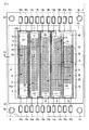
更に、各LEDが発した熱の一部が封止樹脂に伝えられるとともに、封止樹脂内で励起される蛍光体は発熱するが、この封止樹脂の熱の一部を、発光グループに対する熱拡散層の食み出した部位で受けて速やかにモジュール基板に伝導させることができるため、封止樹脂に熱が篭ることが抑制されてLEDの温度上昇を更に抑制できる。
しかも、熱拡散層の発光グループから食み出した部位が蛍光体入りの封止樹脂で覆われているため、前記部位上の封止樹脂に入射された光により励起された蛍光体の放射光の一部を、前記部位で光の利用方向に反射させて光の取出し効率を向上できる。
又、配線導体と熱拡散層が同種の金属製であるので、これら配線導体と熱拡散層を同時に製造できる。
Claims (1)
- モジュール基板と;
前記モジュール基板の表面に設けられて、前記モジュール基板の表面に凹凸を形成するとともに光を反射する複数の配線導体と;
前記複数の配線導体間であって、これら配線導体に隣接して前記モジュール基板の表面の一部に設けられて、前記配線導体とともに前記モジュール基板の表面に凹凸を形成し、かつ、隣接した前記配線導体との間に前記凹凸の凹部を形成するとともに前記配線導体と同種の金属からなり光を反射する熱拡散層と;
前記配線導体を通じて給電されるとともに前記熱拡散層の全長より短い発光グループを形成し、この発光グループから前記熱拡散層が食み出すように前記熱拡散層上に実装された複数個のLEDと;
前記熱拡散層、配線導体、及びLEDを埋めるとともに前記凹部を満たしかつ一部が前記熱拡散層の前記発光グループから食み出した部位に接着して前記モュール基板に被着された蛍光体入りの透光性封止樹脂と;
を具備したことを特徴とする発光モジュール。
Priority Applications (6)
| Application Number | Priority Date | Filing Date | Title |
|---|---|---|---|
| JP2009046739A JP4640514B2 (ja) | 2009-02-27 | 2009-02-27 | 発光モジュール |
| KR1020117019555A KR101267545B1 (ko) | 2009-02-27 | 2010-02-26 | 발광모듈 및 조명장치 |
| CN201080009903.6A CN102334202B (zh) | 2009-02-27 | 2010-02-26 | 发光模块及照明装置 |
| US13/202,689 US8773612B2 (en) | 2009-02-27 | 2010-02-26 | Light emitting module and illumination apparatus |
| EP10746336.6A EP2403017A4 (en) | 2009-02-27 | 2010-02-26 | LIGHT-EMITTING MODULE AND LIGHTING DEVICE |
| PCT/JP2010/053136 WO2010098457A1 (ja) | 2009-02-27 | 2010-02-26 | 発光モジュールおよび照明装置 |
Applications Claiming Priority (1)
| Application Number | Priority Date | Filing Date | Title |
|---|---|---|---|
| JP2009046739A JP4640514B2 (ja) | 2009-02-27 | 2009-02-27 | 発光モジュール |
Related Child Applications (1)
| Application Number | Title | Priority Date | Filing Date |
|---|---|---|---|
| JP2010255672A Division JP5126632B2 (ja) | 2010-11-16 | 2010-11-16 | 発光モジュール |
Publications (3)
| Publication Number | Publication Date |
|---|---|
| JP2010205776A JP2010205776A (ja) | 2010-09-16 |
| JP2010205776A5 JP2010205776A5 (ja) | 2010-10-28 |
| JP4640514B2 true JP4640514B2 (ja) | 2011-03-02 |
Family
ID=42967027
Family Applications (1)
| Application Number | Title | Priority Date | Filing Date |
|---|---|---|---|
| JP2009046739A Expired - Fee Related JP4640514B2 (ja) | 2009-02-27 | 2009-02-27 | 発光モジュール |
Country Status (1)
| Country | Link |
|---|---|
| JP (1) | JP4640514B2 (ja) |
Families Citing this family (12)
| Publication number | Priority date | Publication date | Assignee | Title |
|---|---|---|---|---|
| US8598602B2 (en) | 2009-01-12 | 2013-12-03 | Cree, Inc. | Light emitting device packages with improved heat transfer |
| US7923739B2 (en) | 2009-06-05 | 2011-04-12 | Cree, Inc. | Solid state lighting device |
| US9111778B2 (en) | 2009-06-05 | 2015-08-18 | Cree, Inc. | Light emitting diode (LED) devices, systems, and methods |
| US8860043B2 (en) | 2009-06-05 | 2014-10-14 | Cree, Inc. | Light emitting device packages, systems and methods |
| US8648359B2 (en) * | 2010-06-28 | 2014-02-11 | Cree, Inc. | Light emitting devices and methods |
| US8269244B2 (en) | 2010-06-28 | 2012-09-18 | Cree, Inc. | LED package with efficient, isolated thermal path |
| JP5612991B2 (ja) | 2010-09-30 | 2014-10-22 | シャープ株式会社 | 発光装置及びこれを備えた照明装置 |
| US8610140B2 (en) | 2010-12-15 | 2013-12-17 | Cree, Inc. | Light emitting diode (LED) packages, systems, devices and related methods |
| TW201251140A (en) | 2011-01-31 | 2012-12-16 | Cree Inc | High brightness light emitting diode (LED) packages, systems and methods with improved resin filling and high adhesion |
| WO2012109225A1 (en) | 2011-02-07 | 2012-08-16 | Cree, Inc. | Components and methods for light emitting diode (led) lighting |
| JP5836780B2 (ja) * | 2011-12-02 | 2015-12-24 | 日立アプライアンス株式会社 | 発光ダイオードモジュール及びそれを利用した照明器具 |
| JP2014187392A (ja) * | 2014-06-23 | 2014-10-02 | Sharp Corp | 発光装置及びこれを備えた照明装置 |
Citations (6)
| Publication number | Priority date | Publication date | Assignee | Title |
|---|---|---|---|---|
| JP2006054336A (ja) * | 2004-08-12 | 2006-02-23 | Sanyo Electric Co Ltd | 発光素子 |
| JP2007324275A (ja) * | 2006-05-31 | 2007-12-13 | Toyoda Gosei Co Ltd | 発光装置 |
| JP2008085302A (ja) * | 2006-08-29 | 2008-04-10 | Toshiba Lighting & Technology Corp | 照明装置 |
| JP2008186914A (ja) * | 2007-01-29 | 2008-08-14 | Hitachi Ltd | 線状光源装置、及びバックライト装置 |
| JP2008300210A (ja) * | 2007-05-31 | 2008-12-11 | Toshiba Lighting & Technology Corp | 照明装置 |
| JP2009037796A (ja) * | 2007-07-31 | 2009-02-19 | Toshiba Lighting & Technology Corp | 光源および照明装置 |
-
2009
- 2009-02-27 JP JP2009046739A patent/JP4640514B2/ja not_active Expired - Fee Related
Patent Citations (6)
| Publication number | Priority date | Publication date | Assignee | Title |
|---|---|---|---|---|
| JP2006054336A (ja) * | 2004-08-12 | 2006-02-23 | Sanyo Electric Co Ltd | 発光素子 |
| JP2007324275A (ja) * | 2006-05-31 | 2007-12-13 | Toyoda Gosei Co Ltd | 発光装置 |
| JP2008085302A (ja) * | 2006-08-29 | 2008-04-10 | Toshiba Lighting & Technology Corp | 照明装置 |
| JP2008186914A (ja) * | 2007-01-29 | 2008-08-14 | Hitachi Ltd | 線状光源装置、及びバックライト装置 |
| JP2008300210A (ja) * | 2007-05-31 | 2008-12-11 | Toshiba Lighting & Technology Corp | 照明装置 |
| JP2009037796A (ja) * | 2007-07-31 | 2009-02-19 | Toshiba Lighting & Technology Corp | 光源および照明装置 |
Also Published As
| Publication number | Publication date |
|---|---|
| JP2010205776A (ja) | 2010-09-16 |
Similar Documents
| Publication | Publication Date | Title |
|---|---|---|
| JP4640514B2 (ja) | 発光モジュール | |
| JP5846408B2 (ja) | 発光装置および照明装置 | |
| JP5522462B2 (ja) | 発光装置及び照明装置 | |
| JP5320560B2 (ja) | 光源ユニット及び照明装置 | |
| JP4675906B2 (ja) | 発光素子搭載用基板、発光素子収納用パッケージ、発光装置および照明装置 | |
| TW201424064A (zh) | 發光裝置及照明裝置 | |
| JP2008244165A (ja) | 照明装置 | |
| JP2012134305A (ja) | 発光装置及びそれを用いた照明装置 | |
| US20110309381A1 (en) | Light-emitting device and lighting apparatus | |
| US20110309379A1 (en) | Light-emitting device and luminare | |
| JP2011192703A (ja) | 発光装置及び照明装置 | |
| JP2008166081A (ja) | 照明装置及びこの照明装置を備えた照明器具 | |
| JP5515822B2 (ja) | 発光装置及び照明装置 | |
| JP5447686B2 (ja) | 発光モジュール、および照明器具 | |
| JP5333771B2 (ja) | 発光装置及び照明装置 | |
| WO2012057163A1 (ja) | 発光装置及び照明装置 | |
| JP2010251796A (ja) | 発光モジュール | |
| JP5067631B2 (ja) | 照明装置 | |
| JP2009231397A (ja) | 照明装置 | |
| JP4890576B2 (ja) | 発光モジュール | |
| JP2010080796A (ja) | 照明装置 | |
| JP5769129B2 (ja) | 発光装置及び照明装置 | |
| JP5656051B2 (ja) | 発光装置及び照明装置 | |
| JP2009212126A (ja) | 照明装置 | |
| JP5212178B2 (ja) | 発光モジュール |
Legal Events
| Date | Code | Title | Description |
|---|---|---|---|
| A521 | Request for written amendment filed |
Free format text: JAPANESE INTERMEDIATE CODE: A523 Effective date: 20100707 |
|
| A871 | Explanation of circumstances concerning accelerated examination |
Free format text: JAPANESE INTERMEDIATE CODE: A871 Effective date: 20100707 |
|
| A975 | Report on accelerated examination |
Free format text: JAPANESE INTERMEDIATE CODE: A971005 Effective date: 20100723 |
|
| A131 | Notification of reasons for refusal |
Free format text: JAPANESE INTERMEDIATE CODE: A131 Effective date: 20100727 |
|
| A521 | Request for written amendment filed |
Free format text: JAPANESE INTERMEDIATE CODE: A523 Effective date: 20100924 |
|
| TRDD | Decision of grant or rejection written | ||
| A01 | Written decision to grant a patent or to grant a registration (utility model) |
Free format text: JAPANESE INTERMEDIATE CODE: A01 Effective date: 20101102 |
|
| A01 | Written decision to grant a patent or to grant a registration (utility model) |
Free format text: JAPANESE INTERMEDIATE CODE: A01 |
|
| A61 | First payment of annual fees (during grant procedure) |
Free format text: JAPANESE INTERMEDIATE CODE: A61 Effective date: 20101115 |
|
| R151 | Written notification of patent or utility model registration |
Ref document number: 4640514 Country of ref document: JP Free format text: JAPANESE INTERMEDIATE CODE: R151 |
|
| FPAY | Renewal fee payment (event date is renewal date of database) |
Free format text: PAYMENT UNTIL: 20131210 Year of fee payment: 3 |
|
| LAPS | Cancellation because of no payment of annual fees |