JP4635354B2 - Exposure method, splice error measurement method, and device manufacturing method - Google Patents
Exposure method, splice error measurement method, and device manufacturing method Download PDFInfo
- Publication number
- JP4635354B2 JP4635354B2 JP2001063024A JP2001063024A JP4635354B2 JP 4635354 B2 JP4635354 B2 JP 4635354B2 JP 2001063024 A JP2001063024 A JP 2001063024A JP 2001063024 A JP2001063024 A JP 2001063024A JP 4635354 B2 JP4635354 B2 JP 4635354B2
- Authority
- JP
- Japan
- Prior art keywords
- pattern
- mark
- exposure
- exposure method
- substrate
- Prior art date
- Legal status (The legal status is an assumption and is not a legal conclusion. Google has not performed a legal analysis and makes no representation as to the accuracy of the status listed.)
- Expired - Fee Related
Links
Images


Classifications
-
- G—PHYSICS
- G03—PHOTOGRAPHY; CINEMATOGRAPHY; ANALOGOUS TECHNIQUES USING WAVES OTHER THAN OPTICAL WAVES; ELECTROGRAPHY; HOLOGRAPHY
- G03F—PHOTOMECHANICAL PRODUCTION OF TEXTURED OR PATTERNED SURFACES, e.g. FOR PRINTING, FOR PROCESSING OF SEMICONDUCTOR DEVICES; MATERIALS THEREFOR; ORIGINALS THEREFOR; APPARATUS SPECIALLY ADAPTED THEREFOR
- G03F7/00—Photomechanical, e.g. photolithographic, production of textured or patterned surfaces, e.g. printing surfaces; Materials therefor, e.g. comprising photoresists; Apparatus specially adapted therefor
- G03F7/70—Microphotolithographic exposure; Apparatus therefor
- G03F7/70483—Information management; Active and passive control; Testing; Wafer monitoring, e.g. pattern monitoring
- G03F7/70605—Workpiece metrology
- G03F7/70616—Monitoring the printed patterns
- G03F7/70633—Overlay, i.e. relative alignment between patterns printed by separate exposures in different layers, or in the same layer in multiple exposures or stitching
-
- G—PHYSICS
- G03—PHOTOGRAPHY; CINEMATOGRAPHY; ANALOGOUS TECHNIQUES USING WAVES OTHER THAN OPTICAL WAVES; ELECTROGRAPHY; HOLOGRAPHY
- G03F—PHOTOMECHANICAL PRODUCTION OF TEXTURED OR PATTERNED SURFACES, e.g. FOR PRINTING, FOR PROCESSING OF SEMICONDUCTOR DEVICES; MATERIALS THEREFOR; ORIGINALS THEREFOR; APPARATUS SPECIALLY ADAPTED THEREFOR
- G03F7/00—Photomechanical, e.g. photolithographic, production of textured or patterned surfaces, e.g. printing surfaces; Materials therefor, e.g. comprising photoresists; Apparatus specially adapted therefor
- G03F7/70—Microphotolithographic exposure; Apparatus therefor
- G03F7/70483—Information management; Active and passive control; Testing; Wafer monitoring, e.g. pattern monitoring
- G03F7/70605—Workpiece metrology
- G03F7/70681—Metrology strategies
- G03F7/70683—Mark designs
-
- G—PHYSICS
- G03—PHOTOGRAPHY; CINEMATOGRAPHY; ANALOGOUS TECHNIQUES USING WAVES OTHER THAN OPTICAL WAVES; ELECTROGRAPHY; HOLOGRAPHY
- G03F—PHOTOMECHANICAL PRODUCTION OF TEXTURED OR PATTERNED SURFACES, e.g. FOR PRINTING, FOR PROCESSING OF SEMICONDUCTOR DEVICES; MATERIALS THEREFOR; ORIGINALS THEREFOR; APPARATUS SPECIALLY ADAPTED THEREFOR
- G03F9/00—Registration or positioning of originals, masks, frames, photographic sheets or textured or patterned surfaces, e.g. automatically
- G03F9/70—Registration or positioning of originals, masks, frames, photographic sheets or textured or patterned surfaces, e.g. automatically for microlithography
- G03F9/7003—Alignment type or strategy, e.g. leveling, global alignment
- G03F9/7019—Calibration
-
- G—PHYSICS
- G03—PHOTOGRAPHY; CINEMATOGRAPHY; ANALOGOUS TECHNIQUES USING WAVES OTHER THAN OPTICAL WAVES; ELECTROGRAPHY; HOLOGRAPHY
- G03F—PHOTOMECHANICAL PRODUCTION OF TEXTURED OR PATTERNED SURFACES, e.g. FOR PRINTING, FOR PROCESSING OF SEMICONDUCTOR DEVICES; MATERIALS THEREFOR; ORIGINALS THEREFOR; APPARATUS SPECIALLY ADAPTED THEREFOR
- G03F9/00—Registration or positioning of originals, masks, frames, photographic sheets or textured or patterned surfaces, e.g. automatically
- G03F9/70—Registration or positioning of originals, masks, frames, photographic sheets or textured or patterned surfaces, e.g. automatically for microlithography
- G03F9/7073—Alignment marks and their environment
- G03F9/708—Mark formation
-
- G—PHYSICS
- G03—PHOTOGRAPHY; CINEMATOGRAPHY; ANALOGOUS TECHNIQUES USING WAVES OTHER THAN OPTICAL WAVES; ELECTROGRAPHY; HOLOGRAPHY
- G03F—PHOTOMECHANICAL PRODUCTION OF TEXTURED OR PATTERNED SURFACES, e.g. FOR PRINTING, FOR PROCESSING OF SEMICONDUCTOR DEVICES; MATERIALS THEREFOR; ORIGINALS THEREFOR; APPARATUS SPECIALLY ADAPTED THEREFOR
- G03F9/00—Registration or positioning of originals, masks, frames, photographic sheets or textured or patterned surfaces, e.g. automatically
- G03F9/70—Registration or positioning of originals, masks, frames, photographic sheets or textured or patterned surfaces, e.g. automatically for microlithography
- G03F9/7073—Alignment marks and their environment
- G03F9/7084—Position of mark on substrate, i.e. position in (x, y, z) of mark, e.g. buried or resist covered mark, mark on rearside, at the substrate edge, in the circuit area, latent image mark, marks in plural levels
-
- H—ELECTRICITY
- H10—SEMICONDUCTOR DEVICES; ELECTRIC SOLID-STATE DEVICES NOT OTHERWISE PROVIDED FOR
- H10W—GENERIC PACKAGES, INTERCONNECTIONS, CONNECTORS OR OTHER CONSTRUCTIONAL DETAILS OF DEVICES COVERED BY CLASS H10
- H10W46/00—Marks applied to devices, e.g. for alignment or identification
-
- H—ELECTRICITY
- H10—SEMICONDUCTOR DEVICES; ELECTRIC SOLID-STATE DEVICES NOT OTHERWISE PROVIDED FOR
- H10W—GENERIC PACKAGES, INTERCONNECTIONS, CONNECTORS OR OTHER CONSTRUCTIONAL DETAILS OF DEVICES COVERED BY CLASS H10
- H10W46/00—Marks applied to devices, e.g. for alignment or identification
- H10W46/301—Marks applied to devices, e.g. for alignment or identification for alignment
Landscapes
- Physics & Mathematics (AREA)
- General Physics & Mathematics (AREA)
- Exposure And Positioning Against Photoresist Photosensitive Materials (AREA)
- Preparing Plates And Mask In Photomechanical Process (AREA)
- Exposure Of Semiconductors, Excluding Electron Or Ion Beam Exposure (AREA)
Description
【0001】
【発明の属する技術分野】
本発明は、半導体デバイスや液晶表示デバイス等の製造工程でマスクのパターンを基板上に露光する露光方法及び継ぎ誤差計測方法並びにデバイス製造方法に関し、特に複数の分割パターンの一部同士を基板上で互いにつなぎ合わせることによって大面積のパターンを露光する、いわゆる画面合成を行う際に用いて好適な露光方法及び継ぎ誤差計測方法並びにデバイス製造方法に関するものである。
【0002】
【従来の技術】
従来、この種の露光装置では、露光対象となる感光性基板の大型化に対応するために、感光性基板の露光領域を複数の単位領域(ショット)に分割し、各単位露光領域に対する露光を複数回に亙って繰り返し、最終的に所望の大面積を有するパターンを合成する手法、いわゆる画面合成の手法が用いられている。画面合成を行う場合、パターン投影用のレチクルの描画誤差、投影光学系のディストーション、感光性基板を位置決めするステージの位置決め誤差等に起因して、各単位露光領域の境界位置において継ぎ合わされるパターンに切れ目が発生する事がある。そこで、パターンの切れ目の発生を防止するために、各単位露光領域の境界を微少量だけ重ね合わせることによって、すなわち、各単位露光領域を部分的に重複させることによって画面合成を行う場合もある。
【0003】
このような画面合成を行う際に最も注意しなければならない点は、レチクルの製造誤差や投影光学系のレンズ収差、感光性基板等の試料を位置決めするステージの位置決め精度・走り精度などに起因した画面合成部分のパターン間のずれを極力小さくして画面継ぎ精度を確保することである。すなわち、上記のような画面合成では、隣接する二つのパターンの間の相対位置ずれによってパターンの継ぎ目部分に段差が発生し、製造デバイスの特性が損なわれることがある。さらに、半導体デバイスや液晶表示用デバイス製造では、画面合成された単層のパターンを複数の層(通常、液晶パネル製造では5〜8層)に重ね合わせているため、各層における単位露光領域の重ね合わせ誤差がパターンの継ぎ目部分で不連続に変化することになる。この場合、特にアクティブマトリックス液晶デバイスでは、パターン継ぎ目部分でコントラストが不連続に変化して、デバイスの品質が低下することになる。
【0004】
一般に、第2層以降の露光レイヤーにおける画面継ぎ精度は、ショットとショットとの重ね合わせ精度の差が重要であることが知られているため、例えば第1層に形成されたアライメントマークを計測し、その計測結果から第2層以降のレイヤーにおけるレチクルおよび感光性基板のオフセットを求めて補正すればよい。つまり、第2層(例えば、ソース・ドレイン層)で継ぎ合わせ露光を行う際には、前レイヤーである第1層(例えば、ゲート層)に形成されたアライメントマークという基準が存在するため、このアライメントマークをオフアクシス等のセンサで計測して、継ぎ合わされるソース・ドレイン層のパターンをそれぞれ対応するゲート層のパターンと高精度に重ね合わせるように追い込むことで、結果として第2層でのパターンの継ぎ合わせが高精度に行われる。
【0005】
このように、第2層以降のパターンの継ぎ合わせ精度は、第1層におけるパターンの継ぎ合わせ精度に依存しているが、通常の露光処理では、第1層で画面を継ぎ合わせる際に下地に基準がなく、機械精度やパターンの製造精度に依存して露光が行われるため、継ぎ合わせ精度を高精度に追い込むことが困難である。これに対して従来では、例えば以下の2つの方法により第1層における継ぎ精度を確保していた。
【0006】
(1)プロセス中
レチクル製造誤差や投影光学系のレンズ収差については、図10に示すように、それぞれが2辺で継ぎ合わされるパターンA〜Dにより所望のパネルパターンが画面合成される場合、図11に示すように、レチクル内のパターンA近傍に複数の特殊パターン、具体的には複数の2次元マークを継ぎ合わされる辺に沿って配置し、被露光物である感光性基板が搭載されるステージ側からこれらのマークの位置を測定し、各マークの設計位置と測定結果との位置ずれ誤差を統計処理することで、そのレチクル上のパターンをステージ上で最も理想的な格子状に露光できるように補正パラメータ(シフト、回転、倍率等)を求めていた。なお、このステージ側からマークの位置を計測する方法としては、ステージにスリットマークを有する基準マーク部材を設け、基準マーク部材の下方から露光波長と同一波長の検知光を照射し、ステージを走査移動しながらスリットマーク、投影光学系、レチクル上のマークを介して入射する検知光を光量検出器でモニタすることで、ステージ座標系に対するマークの位置を計測する、いわゆるISS(Image Slit Sensor)計測等を用いることができる。
【0007】
そして、パターンB〜Dについても、パターンAと同様に継ぎ合わされる辺に沿ってマークを配置し、これらのマークの位置を計測することで、各パターンB〜Dを理想格子状に露光できるように補正パラメータを求めていた。また、感光性基板を位置決めするステージの位置決め精度や走り精度については、調整時に誤差を可能な限り小さく追い込むことで画面継ぎ精度を維持していた。
【0008】
(2)テスト露光
プロセス露光を実施する前にパターンA〜Dを画面合成して所望パターンの継ぎ合わせ露光を実施し、その継ぎ合わせ部分を測定器で計測することで、図12に示すように位置ずれ量Zを求め、この位置ずれ量Zを設計値からのずれとして、プロセス露光における露光制御データのレチクル部分にオフセットとして入力する方法があった。
【0009】
【発明が解決しようとする課題】
しかしながら、上述したような従来の露光方法および露光装置には、以下のような問題が存在する。
上記(1)の技術では、実際に転写されるパターンA〜Dを測定していないこと、実際に露光後のパターンを計測していないこと、ISS計測等の光学的原理で計測していること等の理由により、補正パラメータに基づいて露光しても、実際に露光したパターンには設計値からのずれが生じることがあった。これには、幾つかの原因が考えられるが、例えば計測原理に基づく誤差や再現性の限界、プロセス条件に依存した感光性基板の変形、実パターンと計測用マークとの製造誤差などが挙げられる。
【0010】
また、上記(2)の技術では、上述したように第1層で画面合成を行う場合、下地に基準がないため継ぎ合わせ精度を厳しく追い込むことが困難であることに加えて、例えば第1層に露光されたパターンの1つの位置を計測するセンサを別途設け、計測したパターンの位置に基づいて他のパターンを露光する方法を採ったとしても、通常のパターン形状は層毎に、例えばX方向またはY方向の一方向にのみ延在することが多いため、上記パターンの1つの位置をX、Yの両方向で検出することは困難である。そのため、計測できない側の方向(Y方向またはX方向)に関しては、継ぎ合わせ精度を充分に追い込むことが難しい。
【0011】
このような理由により、上記(1)、(2)の技術は、継ぎ合わせ精度の追い込み方法としては必ずしも充分なものではなかった。
【0012】
本発明は、以上のような点を考慮してなされたもので、基板上にパターンを継ぎ合わせて画面合成を行う際に、継ぎ合わせ精度を正確に追い込むことができる露光方法および露光装置を提供することを目的とする。
【0013】
【課題を解決するための手段】
上記の目的を達成するために本発明は、以下の構成を採用している。
本発明の露光方法は、基板上にパターンを露光する露光方法において、第1の基板に第1パターンと第2パターンとを継ぎ合わせて露光する第1露光工程と、所定間隔で配列された複数のマークを含むマーク列を、前記第1露光工程によって継ぎ合わせて露光される前記第1パターンと前記第2パターンとの分割ラインを跨ぐように前記第1の基板に露光する第2露光工程と、前記複数のマークのうち前記第1パターン側に露光されたマークと前記第1パターンとの第1の相対位置関係、及び前記複数のマークのうち前記第2パターン側に露光されたマークと前記第2パターンとの第2の相対位置関係を計測し、該第1及び第2の相対位置関係に基づいて、前記第1パターンと前記第2パターンとの継ぎ誤差を算出する計測工程と、前記計測工程によって算出された前記継ぎ誤差に基づいて前記パターンの露光に関するパラメータを補正し、前記第1パターンと前記第2パターンとを継ぎ合わせて第2の基板に露光する第3露光工程と、を含むことを特徴とするものである。
また、本発明の継ぎ誤差計測方法は、基板上に継ぎ合わせて露光される第1パターンと第2パターンとの継ぎ誤差を計測する継ぎ誤差計測方法であって、所定の間隔で設けられた複数のマークを含むマーク列を、前記基板上における前記第1パターンと前記第2パターンとの分割ラインを跨ぐように前記基板に露光する工程と、前記複数のマークのうち前記第1パターン側に露光されたマークと前記第1パターンとの第1の相対位置関係、及び前記複数のマークのうち前記第2パターン側に露光されたマークと前記第2パターンとの第2の相対位置関係を計測し、該第1及び第2の相対位置関係に基づいて、前記継ぎ誤差を算出する工程とを備えることを特徴とするものである。
そして、本発明のデバイス製造方法は、基板を処理してデバイスを製造するデバイス製造方法であって、本発明に係る態様の露光方法を用いて、前記基板にパターンを転写することと、前記パターンが転写された前記基板を該パターンに基づいて加工することと、を含むものである。
【0014】
また、本発明の露光装置は、基板(P)上にパターン(A〜D)を継ぎ合わせて所望のパターンを露光する露光装置において、基板(P)に露光された、パターン(A〜D)とは異なる第1マーク(MK)と継ぎ合わされるパターン(A〜D)との相対位置関係に基づいて、継ぎ合わされるパターン(A〜D)を露光する際の補正量を記憶する記憶装置(33)と、記憶装置(33)に記憶された補正量に基づいて、パターンを基板(P)上で継ぎ合わせる補正装置(23)とを備えることを特徴とするものである。
【0015】
従って、本発明の露光方法および露光装置では、例えば第1マーク(MK)をX方向およびY方向に延在する二次元マークとして、パターン(A〜D)とともに基板(P)に露光し、露光したパターン(A〜D)および第1マーク(MK)を計測することにより、パターン(A〜D)の継ぎ合わせずれを二次元的に補正量として求めることができる。そのため、実露光において、この補正量で補正した状態でパターンを継ぎ合わせることで、継ぎ合わせ精度を充分に追い込むことができる。しかも、本発明では、補正量を求める際に実際に転写されるパターンを用いているので、実露光時に必要な補正量を直接求めることができる。
【0016】
【発明の実施の形態】
以下、本発明の露光方法および露光装置の実施の形態を、図1ないし図9を参照して説明する。
ここでは、ステッパ方式の露光装置により、感光性基板である液晶表示デバイス製造用のガラスプレート(以下、単にプレートと称する)に複数のレチクルのパターンを正立等倍で画面合成する場合の例を用いて説明する。これらの図において、従来例として示した図10乃至図12と同一の構成要素には同一符号を付し、その説明を省略する。
【0017】
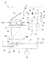
図1は、液晶表示デバイス用露光装置9の概略構成図である。この露光装置9は、レチクル(マスク)Rに形成された液晶表示デバイスのパターンを感光剤(レジスト)が塗布されたプレート(基板)P上に投影露光するものであって、光源10、照明光学系11、投影光学系12、レチクルステージ(マスクステージ)13およびプレートステージ(基板ステージ)14から概略構成されている。ここで、投影光学系12の光軸に平行にZ軸が、光軸に垂直な面内において、図1の紙面に平行にX軸が、光軸に垂直な面内において図1の紙面に垂直にY軸がそれぞれ設定されているものとする。
【0018】
光源10は、露光光としてのビームBを発するものであり、超高圧水銀ランプ等で構成されている。光源10から射出されたビームBは、照明光学系11に入射する。
【0019】
照明光学系11は、ビームBの光路を開閉するシャッタ15と、反射ミラー16、17と、波長選択フィルター18と、ビームBを均一化するためのオプティカルインテグレータ(フライアイレンズ等)19と、可変視野絞り20と、コンデンサ光学系21とから構成されている。シャッタ15は、シャッタ駆動部22を介して制御装置(補正装置)23により制御されることでビームBの光路を開閉するように駆動される。そして、シャッタ15の開動作に応じて照明光学系11に入射したビームBは、波長選択フィルター18において露光に必要な波長(g線やh線、i線)が通過し、オプティカルインテグレータ19で照度が均一化される。照度が均一化されたビームBは、ビームスプリッタ24を透過した後、コンデンサ光学系21で集光され、可変視野絞り20の開口によって規定されるレチクルR上の照明領域を重畳的に照明する。可変視野絞り20の開口の位置および大きさは、不図示のブラインド駆動部を介して制御装置23により制御される。
【0020】
レチクルステージ13は、レチクルRを保持するものであって、レチクルステージ駆動系25によってXY座標系上で二次元に移動可能になっている。また、レチクルステージ13の上方には、光電センサーであるレチクルアライメント系26a、26bが配置されている。レチクルアライメント系26a、26bは、光源10が発するビームBと同じ波長のアライメント光を照射し、その反射光をCCDカメラで受光して画像処理を行うものである。そして、本露光装置では、Cr等で直線状に形成されたレチクルR上のアライメントマークを検出し、この検出結果に基づいてレチクルステージ駆動系25を介してレチクルステージ13を駆動することにより、レチクルRをXY座標系で所定の位置にアライメント(位置合わせ)するようになっている。
【0021】
投影光学系12は、レチクルRの照明領域に存在するパターンの像をプレートP上に結像させる。そして、プレートP上に塗布された感光剤が感光することで、プレートP上にパターン像が転写される。この投影光学系12の結像特性(倍率等)は、制御装置23の制御により調整される。
【0022】
プレートステージ14は、プレートPを保持するものであって、ステージ駆動装置27によってXY座標系上を二次元に移動可能に構成されている。このプレートステージ14上には、移動鏡28が設置されている。そして、プレートステージ14の位置(ひいてはプレートPの位置)は、レーザ干渉計29から出射されたレーザ光が移動鏡28で反射してレーザ干渉計29に入射し、その反射光と入射光との干渉に基づいて正確に計測されるようになっている。このレーザ干渉計29による計測結果は、制御装置23に出力される。なお、説明の便宜上、図1においてはプレートステージ14のX方向の位置を計測するための移動鏡28、レーザ干渉計29のみを示しているが、Y方向の位置を計測するための移動鏡、レーザ干渉計がもう一組備えられている。
【0023】
投影光学系12とプレートステージ14との間には、斜入射型のオートフォーカス系30a、30bが配置されており、プレートPの表面が常に投影光学系12の光軸方向の所定位置になるように位置決めされる。すなわち、プレートPの被露光面が投影光学系12の焦点面に一致するように、プレートステージ14をZ方向に駆動する構成になっている。
【0024】
また、プレートステージ14上には、投影光学系12の光軸方向に関してプレートPの被露光面と略一致する位置に、円盤状の基準マーク部材32が配設されている。この基準マーク部材32には、矩形状の開口のスリットマーク(不図示)が設けられている。そして、プレートステージ14中の基準マーク部材32の下方には、ミラー34およびコンデンサレンズ35が配設され、光ファイバ36によって検出光として伝送されたビームB(露光光)が、コンデンサレンズ35およびミラー34を介して下方から基準マーク部材32に照明されるようになっている。
【0025】
照明された基準マーク部材32上のスリットマークの像は、投影光学系12を介してレチクルR上に逆投影される。そして、レチクルRを透過したビームBは、コンデンサ光学系21、反射ミラー17を介してビームスプリッタ24に入射する。ビームスプリッタ24に入射したビームBは、ここで反射し、光電センサーである光量センサー37に入射する。光量センサー37は、入射したビームBの強度に応じた電気信号を制御装置23に出力する。なお、光量センサー37は、レチクルRと共役な面に配置されている。
【0026】
制御装置23は、光量センサー37から出力された信号とレーザ干渉計29等から出力された信号とを用いてレチクル上のマークの位置を検出するとともに、検出したマークの位置と設計位置とのずれ量を用いて所定の演算処理(最小二乗法等)を実行することで、レチクルRの回転補正量、XYシフト補正量、XY倍率オフセット量等の補正パラメータを算出する。そして、制御装置23は、算出した補正パラメータに基づいて、レチクルステージ駆動系25を介してレチクルRを位置決めするとともに、投影光学系12の結像特性を調整する。
【0027】
また、制御装置23は、上記投影光学系12、シャッタ駆動部22、ブラインド駆動部、レチクルステージ駆動系25、ステージ駆動装置27を統括的に制御しており、プレートステージ14の位置を検出しつつ、プレートステージ14を介してプレートPを二次元的に移動させることにより、プレートP上にレチクルRのパターンを継ぎ合わせて所望のパターンを露光形成する。さらに、制御装置23には、シーケンスパラメータ等の各種露光データ(レシピ)や、補正パラメータ等を記憶する記憶装置33が付設されている(図1参照)。
【0028】
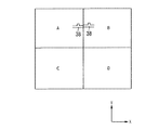
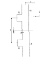
続いて、プロセス処理に先立って実施する処理(予備露光工程)について説明する。この予備露光工程は、プロセス処理で露光されるゲートパターンをプレートPに露光するパターン露光工程と、ゲートパターンが露光されたプレートPにマークMKを露光するマーク露光工程とに大別される。なお、ここでは、図10に示したように、プレートPの第1層にパターンA〜Dが継ぎ合わされてゲート層(ゲートパターン)が画面合成されるものとする。
【0029】
各パターンA〜Dは、図12にも示したように、X方向に延在する走査線パターン(単位パターン)38と、走査線パターン38に沿って所定のピッチLX(例えば100μmのピッチ)で配列された複数のゲート電極パターン(単位パターン)39とがY方向に所定のピッチ(LYとする)で配列された同一のゲートパターンを有しており、パターンA〜Dが継ぎ合わされる分割ラインは通常、走査線パターンと交叉するように設定されている。なお、このゲートパターンは、露光されたプレートPを現像した後に、レジストが当該ゲートパターンでプレートP上に残る、いわゆるポジパターンでレチクルRに形成されている。
【0030】
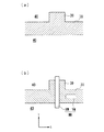
一方、テスト露光に用いられるレチクルRTを図2(a)に示す。
この図に示すように、レチクルRTのほぼ中央には、プロセス処理でプレートPに形成される上記ゲートパターンや他のパターン(ソース・ドレインパターン等)とは異なる第1マークとしてのマークMKが形成されている。図2(b)に示すように、各マークMKは、Y方向に延在してX方向の位置計測に用いられるXマークXMと、X方向に延在してY方向の位置計測に用いられるYマークYMとから構成されている。
【0031】
XマークXMの配列ピッチPXは、ゲート電極パターン39の配列ピッチLXの1/n(nは自然数)に、ここではPX=LK(すなわちn=1)に設定されている。また、YマークYMの配列ピッチPYは、走査線パターン38の配列ピッチLYの1/m(mは自然数)に、ここではPY=LY(すなわちm=1)に設定されている。なお、これらマークMKは、露光されたプレートPを現像した後に、レジストが当該マークMK形状でプレートP上から除去される、いわゆるネガパターンでレチクルRに形成されている。
【0032】
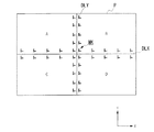
そして、まずパターン露光工程ではゲートパターンを有するレチクルRを用いて、プレートP上の第1層にゲートパターンを露光する。このとき、パターンA〜Dをそれぞれ有する4枚のレチクルを交換しながら、図3に示すように、Y方向に延在する分割ラインDLY、およびX方向に延在する分割ラインDLXでパターンA〜Dを順次継ぎ合わせて露光することでプレートP上にパネルパターンを画面合成する。
【0033】
なお、パターンA〜Dをそれぞれ有する複数のレチクルを用いずに、パネルパターンを構成するゲートパターンやソース・ドレインパターンが一定のピッチで繰り返し配置される形状特性を利用し、可変視野絞り20の駆動を調整することで、1枚のレチクル上の照明領域をパターン毎に変更する手順としてもよい。この場合、レチクルの枚数が減少するとともに、レチクル交換時間を低減することができ、生産効率の向上に寄与できる。
【0034】
次に、テスト露光用レチクルRTをレチクルステージ13上にセットし、プレートステージ14を順次移動させることで、マークMKをプレートPの中心および分割ラインDLY、DLXに沿って各回4つずつ複数回(図3では9回)露光する。なお、このレチクルRTを用いてのマークMKの露光に際しては、プレートPに対するアライメントを行わず、ゲートパターンの露光後に連続して実施することが好ましい。これにより、プレートアライメントに伴う誤差が発生して、継ぎ合わせ精度以外の誤差要因がテスト露光結果に含まれてしまうことを防止できる。
【0035】
このマーク露光工程においてマークMKは、各回の露光において分割ラインDLY(及び/又はDLX)を跨いだ各パターンの双方に露光される。すなわち、マークMKは、プレートP上で隣接して継ぎ合わされるパターンの双方に1度のショットで同時に露光される。また、各マークMKは、図4(a)に示すように、パターン露光工程で形成されたゲートパターンに対して、図4(b)に示すように、XマークXMがゲートパターンの中、ゲート電極パターン39のX方向の中心に位置するように、且つYマークYMがゲートパターンの中、走査線パターン38のY方向の中心に位置するように重ね合わせられる。
【0036】
なお、レチクルR上においてマークMKは、レチクル中央付近、すなわち投影光学系12の光軸近傍に配置されているので、投影光学系12を介して投影される際の倍率やローテーションに起因するレチクル成分の誤差を最も小さくすることができる構成になっている。
【0037】
このように、予備露光工程でプレートP上にゲートパターンおよびマークMKの双方が露光されると、プレートPに現像処理を施す。ここで、ゲートパターンはポジパターンであるため、レチクルR上のゲートパターン以外の領域を透過したビームBにより、プレートP上のレジストは、図4(a)に示すように、ゲートパターンに対応する領域外40が露光され、ゲートパターンに対応した領域(パターン38、39部分)が未露光領域となる。そして、マークMKはネガパターンであるため、図4(b)に示すように、未露光領域であるパターン38、39上に露光形成されることになる。従って、予備露光工程後にプレートPに対して現像処理を実施しても、ゲートパターン内にマークMKが形成されることになる(ただし、図4(b)中、ゲートパターンから突出したXマークXMの両端は現像処理により除去される)。なお、潜像計測が可能であれば、プレートPを現像することなく、予備露光工程後に直ちに後述する計測工程に移行可能である。
【0038】
予備露光工程後においては、プレートPに転写されたゲートパターンとマークMKとの相対位置関係を、例えば重ね合わせ測定器で測定する。具体的には、図5に示すように、例えば分割ラインDLYを挟んでX方向で隣り合うゲートパターンとマークMKとの相対位置関係をパターンA、B側の双方でそれぞれ測定する。
【0039】
ここで、図5に示すパターンA、Bの双方を1つのウィンドウ内に取り込んでエッジ検出する場合、ゲート電極パターン39の配列ピッチLX(図12参照)が画素ピッチで300μm、RGB分割で100μm程度であるため、測定器における対物レンズの検出倍率を大幅に下げる必要に迫られる。しかしながら、検出倍率を下げることは検出分解能を下げることになり、結果として測定精度を下げることになる。従って、本実施の形態では、パターンA、B毎にゲートパターンとマークMKとの相対位置関係を測定することで、せいぜい数十μm程度のエリア計測で充分になり、対物レンズの検出倍率を高めた状態で1つのウィンドウ内でエッジ検出を実行することができる。
【0040】
以下、相対位置計測について詳述する。
例えば、図5中、左側のショット(パターンA)におけるゲートパターンとマークMKとの重ねずれ量は、X方向についてはゲート電極パターン39とXマークXMとの重ねずれ量OVLXとなり、Y方向については走査線パターン38とYマークYMとの重ねずれ量OVLYとなる。同様に、右側のショット(パターンB)におけるゲートパターンとマークMKとの重ねずれ量は、X方向についてはゲート電極パターン39とXマークXMとの重ねずれ量OVRXとなり、Y方向については走査線パターン38とYマークYMとの重ねずれ量OVRYとなる。
【0041】
ここで、マークMKは、一枚のレチクルRT上に形成され、マーク位置およびマーク間の距離を予め計測できるので、プレートP上の位置もゲートパターンに比較して信頼性が高い。そのため、上記の重ねずれ量は、マークMKの位置が基準となり、このマークMKに対するゲートパターンの重ねずれ及び継ぎずれ(継ぎ誤差)と見なすことができる。
【0042】
そして、パターンAとパターンBとの間の継ぎ精度は、測定された上記重ねずれ量を用いた以下の式で表される。
X方向: |OVLX−OVRX|
Y方向: |OVLY−OVRY| …(1)
このように、従来では困難であったX方向およびY方向の双方の継ぎ精度を別途容易に求めることができる。
【0043】
なお、上述したパターンA、B間の継ぎ精度ではなく、例えばY方向に隣接するパターンA、C間の継ぎ精度を求めるには、図示していないものの、分割ラインDLXを挟んでY方向で隣り合うゲートパターンとマークMKとの相対位置関係を上記と同様の手順でパターンA、Cの双方でそれぞれ測定する。そして、上側のショット(パターンA)におけるゲートパターンとマークMKとのX方向の重ねずれ量(OVUXとする)およびY方向の重ねずれ量(OVUYとする)を求めるとともに、下側のショット(パターンC)におけるゲートパターンとマークMKとのX方向の重ねずれ量(OVDXとする)およびY方向の重ねずれ量(OVDYとする)を求め、式(1)に準じた以下の式を用いることで、パターンA、C間の継ぎ精度を求めることができる。
X方向: |OVUX−OVDX|
Y方向: |OVUY−OVDY|
【0044】
また、上記と同様の手順で他の箇所についても、ゲートパターンとマークMKとの重ねずれ量をそれぞれ計測する。そして、例えばパターンAを露光する際の補正量、すなわちパターンAを有するレチクルRを用いて露光する際の補正パラメータ(シフトX、Y、回転、倍率等)は、図6に示すように、複数のマークMKの中、パターンAが継ぎ合わされる辺に沿って形成された複数のマークとゲートパターンとの重ねずれ量と設計値とを最小二乗法等を用いた統計演算処理することにより求められる。同様に、パターンB〜Dを露光する際の補正パラメータを、各パターンが継ぎ合わされる辺に沿って形成されたマークとゲートパターンとの重ねずれ量を用いて求める。
【0045】
これらの補正パラメータは、レチクルRのパターン誤差と投影光学系12のディストーションとを含めて、実際にプレートP上に露光したゲートパターンを用いて算出されるため、これらの誤差を含めた補正が可能になる。このように、計測工程で求められた各パターンA〜D毎の補正パラメータは、記憶装置33に記憶される。
【0046】
予備露光工程および計測工程が終了すると、露光工程(実露光工程)に移行する。予備露光工程で使用された、例えばパターンAを有するレチクルRが不図示の搬送系によりレチクルステージ13上に搬送されると、制御装置23は、まずレチクルR上の照明領域外に形成されたレチクルマーク(不図示)をレチクルアライメント系26a、26bにより計測させ、レチクルステージ駆動系25を介してレチクルR自体のアライメントを行う。
【0047】
次に、制御装置23は、オートフォーカス系30a、30bを用いて、基準マーク部材32およびプレートPを投影光学系12の光軸方向について、レチクルRと共役な位置に位置合わせする。
【0048】
続いて、制御装置23は、設定工程において、記憶装置33から予め求めたレチクルRの回転補正量、XYシフト補正量、XY倍率オフセット量を読み出し、これらの補正パラメータに基づいてレチクルステージ13を介してレチクルRを位置決めするとともに、投影光学系12の結像特性を調整する。これにより、図6に示すように、理想格子Kに対してずれが生じていたレチクルRのパターンAは補正される。
【0049】
レチクルRに対するアライメントが完了したら、パターンAが露光されるべきプレートP上の領域がショット領域に位置決めされるように、ステージ駆動装置27を介してプレートステージ14を駆動し、ビームBでレチクルRを照明してプレートP上の第1層に、ゲートパターンの一部であるパターンAを露光する。この後、パターンAと同様の手順でパターンB〜Dをそれぞれ有する各レチクルに対して、記憶装置33から読み出した補正パラメータを用いてアライメントするとともに、プレートPを位置決めした後に各パターンB〜Dを露光することにより、プレートP上にはパターンA〜Dが継ぎ合わされたパネルパターンが画面合成される。
【0050】
この画面合成により、パターンA〜Dのそれぞれは、あたかもプレートP上の第ゼロ層に形成されたマークMKと高精度に重ね合わされることと同等となり、各パターンA〜Dのそれぞれと第ゼロ層との重ね合わせが高精度に行われることにより、結果としてパターンA〜Dの継ぎ合わせ精度が向上することになる。
【0051】
そして、プレートP上の第2層以降に露光されるパターン(ソース・ドレインパターン等)は、当該パターンを有するレチクルに交換するとともに、第1層のゲートパターン露光時に形成されたプレートアライメントマークを用いて、このレチクルのアライメントおよび投影光学系12の結像特性調整を実施することで、ゲートパターンに高精度に重ね合わされる。なお、第2層以降を第1層に高精度に重ね合わせるためには、プレートアライメントマークを用いる方法の他に、上記のテスト露光を第2層以降に露光されるパターンに対しても実施し、予め当該パターンを継ぎ合わせて露光する際の補正パラメータを求めておく方法も採用することもできる。
【0052】
以上のように本実施の形態の露光方法および露光装置では、予備露光工程においてプロセスで転写されるゲートパターンとマークMKとをプレートP上に露光し、これらの重ねずれ量に基づいて、ゲートパターンを露光する際の補正パラメータを予め求めているので、プレートP上に第ゼロ層が存在してこの第ゼロ層にゲートパターンを重ね合わせて露光する場合と同等の精度で露光することができ、結果として、プレートP上の第1層に複数のパターンを継ぎ合わせる際にも、継ぎ合わせ精度を充分に追い込むことが可能になる。
【0053】
また、本実施の形態では、マークMKを二次元マークとし、継ぎ合わされるパターン毎にマークMKを露光することで、継ぎ合わせ誤差をX方向およびY方向の双方で検出することができる。そのため、予備露光工程ではパターン毎の補正パラメータのみならず、継ぎ合わされるパターン間の相対的な継ぎ合わせ精度も求めることができる。これにより、本実施の形態では、補正パラメータを用いることで各パターンA〜D毎にアライメント精度を追求し結果的に継ぎ合わせ精度を向上させるものとしたが、例えばパターンAを基準としてパターンAに対する相対的な継ぎ合わせ精度を用いてパターンB〜Dの補正パラメータを補正して継ぎ合わせることも可能になる。
【0054】
しかも、本実施の形態では、ゲートパターンをポジパターンとし、マークMKをネガパターンとするとともに、マークMKの配列ピッチを走査線パターン38、ゲート電極パターン39の配列ピッチに対応させてこれらを重ね合わせて露光しているので、重ねずれ量を計測する際の範囲を数十μm程度に狭くすることができる。そのため、測定器における検出倍率を高くした状態でエッジ検出を実行でき、対物レンズ倍率に起因する測定精度の悪化に影響されることなく、より高精度な検出が可能になるとともに、新たな測定器を別途調達することなく、従来より使用されている重ね合わせ測定器等を使用することができ、高精度及び低コスト化に寄与することができる。加えて、本実施の形態では、レチクルRT上のマークMKがレチクル中央付近に配置されているので、投影される際の倍率やローテーションに起因するレチクル成分の誤差を最も小さくすることができ、より高精度の継ぎ合わせを実現することができる。
【0055】
なお、上記実施の形態において、第1マークとしてのマークMKをゲートパターンが形成されたレチクルRとは異なるレチクルRTに形成する構成としたが、これに限定されるものではなく、例えばゲートパターンを有するレチクルRに直接第1マークを形成してもよい。この場合、第1マークをパターンAと離間した隅部に配置する構成となるが、レチクルステージ13が移動可能であれば、第1マークを投影光学系12の光軸近傍に位置決めした状態でテスト露光を実施することで、投影される際の倍率やローテーションに起因するレチクル成分の誤差が最も小さくなるため好ましい。
【0056】
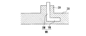
また、上記の実施形態では、ゲートパターンがポジパターンで、第1マークであるマークMKがネガパターンである構成としたが、逆にゲートパターンがネガパターンで第1マークがポジパターンであってもよい。また、第1マークの形状も上述したものに限定されず、X方向およびY方向が共にエッジ検出できれば、図7に示すように、L字形状を呈するマークMKであってもよい。
【0057】
さらに、上記実施の形態では、予備露光工程で一回の露光でマークMKを4つずつプレートP上に露光形成する構成としたが、例えば可変視野絞り20の駆動を制御することで、図8に示すように、継ぎ合わされるパターンに跨って、マークMKを2つずつ個別に露光形成してもよい。また、上記実施の形態では、継ぎ合わされるパターンA〜Dが同一のゲートパターンを有するものとして説明したが、これに限られず、互いに異なるパターン同士を継ぎ合わせる場合にも適用可能である。
【0058】
なお、本実施の形態の基板としては、液晶表示デバイス用のガラスプレートPのみならず、半導体デバイス用の半導体ウエハや、薄膜磁気ヘッド用のセラミックウエハ、あるいは露光装置で用いられるマスクまたはレチクルの原版(合成石英、シリコンウエハ)等が適用される。
【0059】
露光装置9としては、レチクルRとプレートPとを静止した状態でレチクルRのパターンを露光し、プレートPを順次ステップ移動させるステップ・アンド・リピート方式の露光装置(ステッパー)の他に、レチクルRとプレートPとを同期移動してレチクルRのパターンを走査露光するステップ・アンド・スキャン方式の走査型露光装置(スキャニング・ステッパー;USP5,473,410)にも適用することができる。
【0060】
露光装置9の種類としては、プレートPに液晶表示デバイスパターンを露光する液晶表示デバイス製造用の露光装置に限られず、ウエハに半導体デバイスパターンを露光する半導体デバイス製造用の露光装置や、薄膜磁気ヘッド、撮像素子(CCD)あるいはレチクルなどを製造するための露光装置などにも広く適用できる。
【0061】
また、ビームBの光源10として、超高圧水銀ランプから発生する輝線(g線(436nm)、h線(404.7nm)、i線(365nm))、KrFエキシマレーザ(248nm)、ArFエキシマレーザ(193nm)、F2レーザ(157nm)のみならず、X線や電子線などの荷電粒子線を用いることができる。例えば、電子線を用いる場合には電子銃として、熱電子放射型のランタンヘキサボライト(LaB6)、タンタル(Ta)を用いることができる。さらに、電子線を用いる場合は、レチクルRを用いる構成としてもよいし、レチクルRを用いずに直接ガラス基板上にパターンを形成する構成としてもよい。また、YAGレーザや半導体レーザ等の高周波などを用いてもよい。
【0062】
投影光学系12の倍率は、等倍系のみならず縮小系および拡大系のいずれでもよい。また、投影光学系12としては、エキシマレーザなどの遠紫外線を用いる場合は硝材として石英や蛍石などの遠紫外線を透過する材料を用い、F2レーザやX線を用いる場合は反射屈折系または屈折系の光学系にし(レチクルRも反射型タイプのものを用いる)、また電子線を用いる場合には光学系として電子レンズおよび偏向器からなる電子光学系を用いればよい。なお、電子線が通過する光路は、真空状態にすることはいうまでもない。また、投影光学系12を用いることなく、レチクルRとプレートPとを密接させてレチクルRのパターンを露光するプロキシミティ露光装置にも適用可能である。さらに、上記実施の形態では、投影光学系12をシングルレンズとして図示したが、投影領域が互いに重複するように投影レンズを複数配置した、いわゆるマルチレンズ方式の投影光学系であってもよい。
【0063】
プレートステージ14やレチクルステージ13にリニアモータ(USP5,623,853またはUSP5,528,118参照)を用いる場合は、エアベアリングを用いたエア浮上型およびローレンツ力またはリアクタンス力を用いた磁気浮上型のどちらを用いてもよい。また、各ステージ13、14は、ガイドに沿って移動するタイプでもよく、ガイドを設けないガイドレスタイプであってもよい。
【0064】
各ステージ13、14の駆動機構としては、二次元に磁石を配置した磁石ユニット(永久磁石)と、二次元にコイルを配置した電機子ユニットとを対向させ電磁力により各ステージ13、14を駆動する平面モータを用いてもよい。この場合、磁石ユニットと電機子ユニットとのいずれか一方をステージ13、14に接続し、磁石ユニットと電機子ユニットとの他方をステージ13、14の移動面側(ベース)に設ければよい。
【0065】
プレートステージ14の移動により発生する反力は、投影光学系12に伝わらないように、特開平8−166475号公報(USP5,528,118)に記載されているように、フレーム部材を用いて機械的に床(大地)に逃がしてもよい。本発明はこのような構造を備えた露光装置においても適用可能である。
レチクルステージ13の移動により発生する反力は、投影光学系12に伝わらないように、特開平8−330224号公報(US S/N 08/416,558)に記載されているように、フレーム部材を用いて機械的に床(大地)に逃がしてもよい。本発明はこのような構造を備えた露光装置においても適用可能である。
【0066】
以上のように、本願実施形態の基板処理装置である露光装置9は、本願特許請求の範囲に挙げられた各構成要素を含む各種サブシステムを、所定の機械的精度、電気的精度、光学的精度を保つように、組み立てることで製造される。これら各種精度を確保するために、この組み立ての前後には、各種光学系については光学的精度を達成するための調整、各種機械系については機械的精度を達成するための調整、各種電気系については電気的精度を達成するための調整が行われる。各種サブシステムから露光装置への組み立て工程は、各種サブシステム相互の、機械的接続、電気回路の配線接続、気圧回路の配管接続等が含まれる。この各種サブシステムから露光装置への組み立て工程の前に、各サブシステム個々の組み立て工程があることはいうまでもない。各種サブシステムの露光装置への組み立て工程が終了したら、総合調整が行われ、露光装置全体としての各種精度が確保される。なお、露光装置の製造は温度およびクリーン度等が管理されたクリーンルームで行うことが望ましい。
【0067】
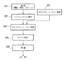
液晶表示デバイスや半導体デバイス等のデバイスは、図9に示すように、液晶表示デバイス等の機能・性能設計を行うステップ201、この設計ステップに基づいたレチクルR(マスク)を製作するステップ202、石英等からガラスプレートP、またはシリコン材料からウエハを製作するステップ203、前述した実施の形態の露光装置9によりレチクルRのパターンをガラスプレートP(またはウエハ)に露光するステップ204、液晶表示デバイス等を組み立てるステップ(ウエハの場合、ダイシング工程、ボンディング工程、パッケージ工程を含む)205、検査ステップ206等を経て製造される。
【0068】
【発明の効果】
以上説明したように、請求項1に係る露光方法は、継ぎ合わされるパターンと第1マークとを基板に露光した後に、第1マークとパターンとの相対位置関係に基づいて、継ぎ合わされるパターンを露光する際の補正量を設定する手順となっている。
これにより、この露光方法では、基板上にに複数のパターンを継ぎ合わせる際にも、継ぎ合わせ精度を充分に追い込むことができるという効果を奏する。
【0069】
請求項2に係る露光方法は、継ぎ合わされるパターン毎に第1マークを露光する手順となっている。
これにより、この露光方法では、パターン毎の補正パラメータのみならず、継ぎ合わされるパターン間の相対的な継ぎ合わせ精度も求めることができるため、基準となるパターンに対する相対的な継ぎ合わせ精度を用いて他のパターンの補正パラメータを補正して継ぎ合わせることも可能になるという効果を奏する。
【0070】
請求項3に係る露光方法は、第1マークが単位パターンの配列ピッチに対応して配列される構成となっている。
これにより、この露光方法では、第1マークと単位パターンとの重ねずれ量を計測する際の範囲を数十μm程度に狭くすることができ、測定器における検出倍率を高くした状態でエッジ検出を実行することで、対物レンズ倍率に起因する測定精度の悪化に影響されることなくより高精度な検出が可能になるという効果が得られる。
【0071】
請求項4に係る露光方法は、第1マークとパターンとを重ね合わせて露光する手順となっている。
これにより、この露光方法では、第1マークと単位パターンとの重ねずれ量を計測する際の範囲を数十μm程度に狭くすることができ、測定器における検出倍率を高くした状態でエッジ検出を実行することで、対物レンズ倍率に起因する測定精度の悪化に影響されることなくより高精度な検出が可能になるという効果が得られる。
【0072】
請求項5に係る露光方法は、パターンがネガパターンとポジパターンとのいずれか一方であり、第1マークがネガパターンとポジパターンとのいずれか他方である構成となっている。
これにより、この露光方法では、第1マークと単位パターンとの重ねずれ量を計測する際の範囲を数十μm程度に狭くすることができ、測定器における検出倍率を高くした状態でエッジ検出を実行することで、対物レンズ倍率に起因する測定精度の悪化に影響されることなくより高精度な検出が可能になるという効果が得られる。
【0073】
請求項6に係る露光方法は、パターンが基板の第1層に形成される手順となっている。
これにより、この露光方法では、基板に基準となるパターンが形成されていない場合でも、複数のパターンを継ぎ合わせる際の継ぎ合わせ精度を充分に追い込むことができるという効果を奏する。
【0074】
請求項7に係る露光方法は、第1マークがマスクの中央に形成される構成となっている。
これにより、この露光方法では、第1マークが投影される際の倍率やローテーションに起因するマスク成分の誤差を最も小さくすることができ、より高精度の継ぎ合わせを実現できるという効果を奏する。
【0075】
請求項8に係る露光方法は、継ぎ合わされるパターンが同一のパターンである構成となっている。
これにより、この露光方法では、基板上に同一のパターンを継ぎ合わせる際にも、継ぎ合わせ精度を充分に追い込むことができるという効果を奏する。
【0076】
請求項9に係る露光装置は、第1マークとパターンとの相対位置関係に基づいて、継ぎ合わされるパターンを露光する際の補正量を記憶し、記憶した補正量に基づいてパターンを基板上で継ぎ合わせる構成となっている。
これにより、この露光装置では、基板上にに複数のパターンを継ぎ合わせる際にも、継ぎ合わせ精度を充分に追い込むことができるという効果を奏する。
【図面の簡単な説明】
【図1】 本発明の実施の形態を示す図であって、露光装置の概略構成図である。
【図2】 (a)は本発明の露光方法に用いられるマークを有するレチクルの平面図であり、(b)はマークの詳細図である。
【図3】 基板上に複数のパターンとマークとが露光された平面図である。
【図4】 (a)はゲートパターンの部分拡大図、(b)はゲートパターンとマークとが重ね合わされた部分拡大図である。
【図5】 分割ラインを挟んで露光されたゲートパターンとマークの部分拡大図である。
【図6】 理想格子とパターンとの相対位置関係を示す図である。
【図7】 他の形状を呈するマークとゲートパターンとが重ね合わされた部分拡大図である。
【図8】 別のマークの露光方法を説明する図である。
【図9】 液晶表示(半導体)デバイスの製造工程の一例を示すフローチャート図である。
【図10】 複数のパターンが継ぎ合わされること示す図である。
【図11】 レチクルに形成されたパターンおよび2次元マークを示す平面図である。
【図12】 継ぎ合わされたパターンにずれが発生していることを示す図である。
【符号の説明】
A〜D パターン
MK マーク(第1マーク)
P ガラスプレート(プレート、基板)
R レチクル(マスク)
9 露光装置
23 制御装置(補正装置)
33 記憶装置
38 走査線パターン(単位パターン)
39 ゲート電極パターン(単位パターン)[0001]
BACKGROUND OF THE INVENTION
The present invention relates to an exposure method for exposing a mask pattern onto a substrate in a manufacturing process of a semiconductor device, a liquid crystal display device, or the like.And joint error measuring method and device manufacturing methodIn particular, an exposure method suitable for use in so-called screen synthesis, in which a large area pattern is exposed by connecting a part of a plurality of divided patterns to each other on a substrate.And joint error measuring method and device manufacturing methodIt is about.
[0002]
[Prior art]
Conventionally, in this type of exposure apparatus, the exposure area of the photosensitive substrate is divided into a plurality of unit areas (shots) in order to cope with an increase in the size of the photosensitive substrate to be exposed, and exposure to each unit exposure area is performed. A technique of repeating a plurality of times and finally synthesizing a pattern having a desired large area, that is, a so-called screen synthesis technique is used. When performing screen composition, due to pattern drawing reticle drawing error, projection optical system distortion, photosensitive substrate positioning error, etc., the pattern stitched at the boundary position of each unit exposure area A break may occur. Therefore, in order to prevent the occurrence of pattern breaks, the screen composition may be performed by superimposing only a small amount of boundaries between the unit exposure areas, that is, by partially overlapping the unit exposure areas.
[0003]
The most important points to consider when performing such screen composition are due to reticle manufacturing errors, lens aberrations of the projection optical system, positioning accuracy and running accuracy of the stage for positioning the sample such as the photosensitive substrate, etc. This is to ensure the screen joining accuracy by minimizing the deviation between the patterns in the screen composition portion. That is, in the screen composition as described above, a difference in position between two adjacent patterns may cause a step at the joint portion of the pattern, which may impair the characteristics of the manufacturing device. Furthermore, in the manufacture of semiconductor devices and liquid crystal display devices, a single layer pattern synthesized on the screen is superimposed on a plurality of layers (usually 5 to 8 layers in the manufacture of liquid crystal panels), so that the unit exposure areas in each layer are overlapped. The alignment error changes discontinuously at the joint portion of the pattern. In this case, particularly in an active matrix liquid crystal device, the contrast changes discontinuously at the pattern seam, and the quality of the device deteriorates.
[0004]
In general, it is known that the difference in overlay accuracy between shots is important for screen joint accuracy in the second and subsequent exposure layers. For example, an alignment mark formed on the first layer is measured. The offset of the reticle and the photosensitive substrate in the second and subsequent layers may be obtained from the measurement result and corrected. That is, when performing joint exposure on the second layer (for example, the source / drain layer), there is a reference called an alignment mark formed on the first layer (for example, the gate layer) which is the previous layer. The alignment mark is measured by a sensor such as off-axis, and the pattern of the source and drain layers to be joined is driven to overlap with the corresponding gate layer pattern with high accuracy, resulting in a pattern on the second layer. Are joined with high accuracy.
[0005]
As described above, the pattern splicing accuracy after the second layer depends on the pattern splicing accuracy in the first layer. However, in normal exposure processing, when the screen is spliced in the first layer, the pattern is used as a base. Since there is no standard and exposure is performed depending on the mechanical accuracy and pattern manufacturing accuracy, it is difficult to drive the splicing accuracy to high accuracy. On the other hand, conventionally, for example, the following two methods ensure the splicing accuracy in the first layer.
[0006]
(1) In process
As shown in FIG. 10, the reticle manufacturing error and the lens aberration of the projection optical system are as shown in FIG. 11 when a desired panel pattern is synthesized by the patterns A to D joined together on two sides. In the vicinity of the pattern A in the reticle, a plurality of special patterns, specifically, a plurality of two-dimensional marks, are arranged along the side where the two-dimensional marks are spliced together, and from the stage side on which the photosensitive substrate as the object to be exposed is mounted. By measuring the position of the mark and statistically processing the misalignment error between the design position of each mark and the measurement result, the correction parameter (in order to expose the pattern on the reticle to the most ideal grid on the stage) Shift, rotation, magnification, etc.). As a method of measuring the position of the mark from the stage side, a reference mark member having a slit mark is provided on the stage, the detection light having the same wavelength as the exposure wavelength is irradiated from below the reference mark member, and the stage is scanned and moved. While detecting the incident detection light through the slit mark, projection optical system, and mark on the reticle with a light amount detector, the position of the mark relative to the stage coordinate system is measured, so-called ISS (Image Slit Sensor) measurement, etc. Can be used.
[0007]
As for the patterns B to D, marks are arranged along the sides to be joined together in the same manner as the pattern A, and by measuring the positions of these marks, the patterns B to D can be exposed in an ideal lattice shape. The correction parameter was obtained. As for the positioning accuracy and running accuracy of the stage for positioning the photosensitive substrate, the screen splicing accuracy is maintained by driving the error as small as possible during adjustment.
[0008]
(2) Test exposure
Before performing the process exposure, the patterns A to D are synthesized on the screen, and the desired pattern is subjected to splicing exposure, and the spliced portion is measured with a measuring instrument. There has been a method in which this positional deviation amount Z is input as an offset to the reticle portion of the exposure control data in the process exposure as a deviation from the design value.
[0009]
[Problems to be solved by the invention]
However, the conventional exposure method and exposure apparatus as described above have the following problems.
In the technique (1), the patterns A to D that are actually transferred are not measured, the pattern after the exposure is not actually measured, and the measurement is performed by optical principles such as ISS measurement. For these reasons, even if exposure is performed based on the correction parameter, the actually exposed pattern may deviate from the design value. There are several possible causes for this, such as errors based on measurement principles and limits of reproducibility, deformation of the photosensitive substrate depending on the process conditions, and manufacturing errors between the actual pattern and the measurement mark. .
[0010]
In the technique (2), when screen composition is performed on the first layer as described above, since there is no reference on the ground, it is difficult to strictly pursue the seaming accuracy. Even if a sensor for measuring one position of the exposed pattern is separately provided and another pattern is exposed based on the measured pattern position, the normal pattern shape is, for example, in the X direction for each layer. Or, since it often extends only in one direction in the Y direction, it is difficult to detect one position of the pattern in both the X and Y directions. For this reason, it is difficult to sufficiently pursue the seaming accuracy with respect to the direction that cannot be measured (Y direction or X direction).
[0011]
For these reasons, the techniques (1) and (2) are not always sufficient as a method for driving the seaming accuracy.
[0012]
The present invention has been made in consideration of the above points, and provides an exposure method and an exposure apparatus capable of accurately tracking the splicing accuracy when performing screen composition by splicing patterns on a substrate. The purpose is to do.
[0013]
[Means for Solving the Problems]
In order to achieve the above object, the present invention employs the following configuration.
The exposure method of the present invention is performed on a substrate.ToIn an exposure method for exposing a turn,A first exposure process in which the first pattern and the second pattern are joined and exposed on the first substrate, and a mark row including a plurality of marks arranged at a predetermined interval are joined together in the first exposure process. A second exposure step of exposing the first substrate so as to straddle a dividing line of the first pattern and the second pattern, and a mark exposed on the first pattern side among the plurality of marks, A first relative positional relationship with the first pattern, and a second relative positional relationship between a mark exposed on the second pattern side of the plurality of marks and the second pattern, and measuring the first relative positional relationship. And a measurement step of calculating a joint error between the first pattern and the second pattern based on the second relative positional relationship, and exposure of the pattern based on the joint error calculated by the measurement step. A third exposure step to correct the parameters, is exposed to a second substrate by joining a said first pattern and said second pattern of, Including.
The splicing error measuring method of the present invention is a splicing error measuring method for measuring a splicing error between a first pattern and a second pattern that are spliced and exposed on a substrate, and is a plurality of splicing errors provided at predetermined intervals. A step of exposing a mark row including the mark to the substrate so as to straddle a dividing line of the first pattern and the second pattern on the substrate, and exposing the mark pattern to the first pattern side of the plurality of marks A first relative positional relationship between the marked mark and the first pattern, and a second relative positional relationship between the mark exposed on the second pattern side of the plurality of marks and the second pattern. And a step of calculating the splicing error based on the first and second relative positional relationships.
And the device manufacturing method of this invention is a device manufacturing method which processes a board | substrate and manufactures a device, Comprising: Transferring a pattern to the said board | substrate using the exposure method of the aspect which concerns on this invention, The said pattern And processing the substrate on which is transferred based on the pattern.
[0014]
Moreover, the exposure apparatus of this invention is a pattern (AD) exposed to the board | substrate (P) in the exposure apparatus which bonds a pattern (AD) on a board | substrate (P), and exposes a desired pattern. A storage device for storing a correction amount when exposing the patterns (A to D) to be joined based on the relative positional relationship between the patterns (A to D) to be joined together with the first mark (MK) different from FIG. 33) and a correction device (23) for joining the patterns on the substrate (P) based on the correction amount stored in the storage device (33).
[0015]
Therefore, in the exposure method and exposure apparatus of the present invention, for example, the first mark (MK) is exposed to the substrate (P) together with the patterns (A to D) as a two-dimensional mark extending in the X direction and the Y direction. By measuring the pattern (A to D) and the first mark (MK), the seam deviation of the pattern (A to D) can be obtained two-dimensionally as a correction amount. Therefore, in the actual exposure, the joining accuracy can be sufficiently driven by joining the patterns in a state corrected with this correction amount. In addition, in the present invention, since a pattern that is actually transferred when the correction amount is obtained is used, the correction amount necessary at the time of actual exposure can be directly obtained.
[0016]
DETAILED DESCRIPTION OF THE INVENTION
Embodiments of the exposure method and exposure apparatus of the present invention will be described below with reference to FIGS.
Here, an example in which a stepper type exposure apparatus synthesizes a plurality of reticle patterns on a glass plate for manufacturing a liquid crystal display device (hereinafter simply referred to as a plate), which is a photosensitive substrate, at an equal magnification. It explains using. In these drawings, the same components as those shown in FIGS. 10 to 12 shown as conventional examples are denoted by the same reference numerals, and the description thereof is omitted.
[0017]
FIG. 1 is a schematic block diagram of an exposure apparatus 9 for a liquid crystal display device. The exposure apparatus 9 projects and exposes a liquid crystal display device pattern formed on a reticle (mask) R onto a plate (substrate) P coated with a photosensitive agent (resist), and includes a
[0018]
The
[0019]
The illumination
[0020]
The
[0021]
The projection
[0022]
The
[0023]
An oblique incidence
[0024]
On the
[0025]
The illuminated slit mark image on the
[0026]
The
[0027]
The
[0028]
Next, a process (preliminary exposure process) performed prior to the process process will be described. This pre-exposure process is roughly divided into a pattern exposure process in which the gate pattern exposed in the process processing is exposed on the plate P, and a mark exposure process in which the mark MK is exposed on the plate P on which the gate pattern is exposed. Here, as shown in FIG. 10, it is assumed that the patterns A to D are joined to the first layer of the plate P, and the gate layer (gate pattern) is synthesized on the screen.
[0029]
As shown in FIG. 12, each of the patterns A to D has a scanning line pattern (unit pattern) 38 extending in the X direction and a predetermined pitch LX (for example, a pitch of 100 μm) along the
[0030]
On the other hand, a reticle RT used for test exposure is shown in FIG.
As shown in this figure, a mark MK as a first mark different from the gate pattern and other patterns (source / drain patterns, etc.) formed on the plate P by the process is formed in the approximate center of the reticle RT. Has been. As shown in FIG. 2B, each mark MK extends in the Y direction and is used for position measurement in the X direction, and is extended in the X direction and used for position measurement in the Y direction. Y mark YM.
[0031]
The arrangement pitch PX of the X marks XM is set to 1 / n (n is a natural number) of the arrangement pitch LX of the
[0032]
First, in the pattern exposure step, the gate pattern is exposed on the first layer on the plate P using the reticle R having the gate pattern. At this time, while exchanging the four reticles each having the patterns A to D, as shown in FIG. 3, the pattern A to the division line DLY extending in the Y direction and the division line DLX extending in the X direction. A panel pattern is synthesized on the plate P by sequentially joining D and exposing.
[0033]
The
[0034]
Next, the test exposure reticle RT is set on the
[0035]
In this mark exposure step, the mark MK is exposed to both of the patterns straddling the dividing line DLY (and / or DLX) in each exposure. That is, the mark MK is simultaneously exposed in one shot to both of the patterns that are joined together on the plate P. Further, as shown in FIG. 4A, each mark MK is different from the gate pattern formed in the pattern exposure process in that the X mark XM is included in the gate pattern as shown in FIG. 4B. The Y pattern YM is overlapped in the gate pattern so as to be positioned at the center in the Y direction of the
[0036]
On the reticle R, the mark MK is arranged in the vicinity of the center of the reticle, that is, in the vicinity of the optical axis of the projection
[0037]
Thus, when both the gate pattern and the mark MK are exposed on the plate P in the pre-exposure step, the plate P is developed. Here, since the gate pattern is a positive pattern, the resist on the plate P corresponds to the gate pattern as shown in FIG. 4A by the beam B transmitted through the region other than the gate pattern on the reticle R. The
[0038]
After the preliminary exposure step, the relative positional relationship between the gate pattern transferred to the plate P and the mark MK is measured by, for example, an overlay measuring device. Specifically, as shown in FIG. 5, for example, the relative positional relationship between the gate pattern adjacent in the X direction and the mark MK across the division line DLY is measured on both the patterns A and B sides.
[0039]
Here, when both the patterns A and B shown in FIG. 5 are taken in one window and edge detection is performed, the arrangement pitch LX (see FIG. 12) of the
[0040]
Hereinafter, the relative position measurement will be described in detail.
For example, in FIG. 5, the amount of overlap between the gate pattern and the mark MK in the left shot (pattern A) is the amount of overlap OVL between the
[0041]
Here, since the mark MK is formed on one reticle RT and the mark position and the distance between the marks can be measured in advance, the position on the plate P is also more reliable than the gate pattern. For this reason, the amount of overlay deviation described above is based on the position of the mark MK, and can be regarded as an overlay deviation and a joint deviation (joint error) of the gate pattern with respect to the mark MK.
[0042]
And the splicing accuracy between the pattern A and the pattern B is expressed by the following equation using the measured overlay deviation amount.
X direction: | OVLX-OVRX|
Y direction: | OVLY-OVRY| (1)
In this way, the joint accuracy in both the X direction and the Y direction, which has been difficult in the past, can be easily obtained separately.
[0043]
For example, in order to obtain the joint accuracy between the patterns A and C adjacent in the Y direction instead of the joint accuracy between the patterns A and B described above, although not shown, they are adjacent in the Y direction across the dividing line DLX. The relative positional relationship between the matching gate pattern and the mark MK is measured for both patterns A and C in the same procedure as described above. Then, the overlay deviation amount (OVU) in the X direction between the gate pattern and the mark MK in the upper shot (pattern A).XAnd overlay displacement in the Y direction (OVU)YAnd the overlay deviation amount (OVD) in the X direction between the gate pattern and the mark MK in the lower shot (pattern C).XAnd the amount of misalignment in the Y direction (OVD)YAnd the following equation according to equation (1) can be used to obtain the joint accuracy between the patterns A and C.
X direction: | OVUX-OVDX|
Y direction: | OVUY-OVDY|
[0044]
In addition, the amount of overlap between the gate pattern and the mark MK is also measured at other locations in the same procedure as described above. For example, as shown in FIG. 6, the correction amount when exposing the pattern A, that is, the correction parameters (shift X, Y, rotation, magnification, etc.) when exposing using the reticle R having the pattern A are plural. Among these marks MK, the amount of overlap between the plurality of marks formed along the side where the pattern A is spliced and the gate pattern and the design value are obtained by performing statistical calculation processing using a least square method or the like. . Similarly, the correction parameters for exposing the patterns B to D are obtained by using the amount of misalignment between the mark formed along the side where the patterns are joined and the gate pattern.
[0045]
Since these correction parameters are calculated using the gate pattern actually exposed on the plate P including the pattern error of the reticle R and the distortion of the projection
[0046]
When the preliminary exposure process and the measurement process are completed, the process proceeds to an exposure process (actual exposure process). When the reticle R having, for example, the pattern A used in the pre-exposure process is transported onto the
[0047]
Next, the
[0048]
Subsequently, in the setting step, the
[0049]
When the alignment with respect to the reticle R is completed, the
[0050]
By this screen composition, each of the patterns A to D is equivalent to being overlaid with high precision with the mark MK formed on the zero layer on the plate P, and each of the patterns A to D and the zero layer As a result, the joining accuracy of the patterns A to D is improved.
[0051]
A pattern (source / drain pattern, etc.) exposed after the second layer on the plate P is replaced with a reticle having the pattern, and a plate alignment mark formed at the time of the first layer gate pattern exposure is used. Thus, the alignment of the reticle and the adjustment of the imaging characteristics of the projection
[0052]
As described above, in the exposure method and exposure apparatus according to the present embodiment, the gate pattern and the mark MK transferred in the process in the preliminary exposure step are exposed on the plate P, and the gate pattern is based on the amount of misalignment. Since the correction parameter for the exposure is determined in advance, the zero layer exists on the plate P, and the exposure can be performed with the same accuracy as the case where the gate pattern is superimposed on the zero layer for exposure. As a result, when joining a plurality of patterns to the first layer on the plate P, it is possible to sufficiently pursue the joining accuracy.
[0053]
In the present embodiment, the mark MK is a two-dimensional mark, and the mark MK is exposed for each pattern to be joined, so that the joining error can be detected in both the X direction and the Y direction. Therefore, in the preliminary exposure step, not only the correction parameters for each pattern but also the relative seaming accuracy between the seamed patterns can be obtained. Thus, in the present embodiment, the correction parameter is used to pursue alignment accuracy for each of the patterns A to D, and as a result, the splicing accuracy is improved. It is also possible to correct the correction parameters of the patterns B to D by using the relative seaming accuracy and perform seaming.
[0054]
In addition, in the present embodiment, the gate pattern is a positive pattern, the mark MK is a negative pattern, and the mark MK is arranged so as to correspond to the arrangement pitch of the
[0055]
In the above embodiment, the mark MK as the first mark is formed on the reticle RT different from the reticle R on which the gate pattern is formed. However, the present invention is not limited to this. The first mark may be directly formed on the reticle R having the same. In this case, the first mark is arranged at a corner away from the pattern A. However, if the
[0056]
In the above embodiment, the gate pattern is a positive pattern and the mark MK as the first mark is a negative pattern. Conversely, even if the gate pattern is a negative pattern and the first mark is a positive pattern. Good. Further, the shape of the first mark is not limited to that described above, and may be an L-shaped mark MK as shown in FIG. 7 as long as both edges in the X direction and the Y direction can be detected.
[0057]
Furthermore, in the above-described embodiment, the mark MK is exposed and formed on the plate P by four exposures in a single exposure in the pre-exposure step. However, for example, by controlling the driving of the
[0058]
The substrate of the present embodiment includes not only a glass plate P for liquid crystal display devices but also a semiconductor wafer for semiconductor devices, a ceramic wafer for thin film magnetic heads, or an original mask or reticle used in an exposure apparatus. (Synthetic quartz, silicon wafer) or the like is applied.
[0059]
As the exposure apparatus 9, in addition to a step-and-repeat type exposure apparatus (stepper) that exposes the pattern of the reticle R while the reticle R and the plate P are stationary and sequentially moves the plate P stepwise, the reticle R And a scanning exposure apparatus (scanning stepper; USP5, 473, 410) of a step-and-scan method that scans and exposes the pattern of the reticle R by moving the P and the plate P synchronously.
[0060]
The type of the exposure apparatus 9 is not limited to an exposure apparatus for manufacturing a liquid crystal display device that exposes a liquid crystal display device pattern on the plate P. An exposure apparatus for manufacturing a semiconductor device that exposes a semiconductor device pattern on a wafer, or a thin film magnetic head The present invention can be widely applied to an exposure apparatus for manufacturing an image pickup device (CCD) or a reticle.
[0061]
As the
[0062]
The magnification of the projection
[0063]
When using a linear motor (see USP5,623,853 or USP5,528,118) for the
[0064]
As a drive mechanism for each
[0065]
As described in JP-A-8-166475 (USP 5,528,118), the reaction force generated by the movement of the
As described in JP-A-8-330224 (US S / N 08 / 416,558), a frame member is used so that the reaction force generated by the movement of the
[0066]
As described above, the exposure apparatus 9 which is the substrate processing apparatus according to the embodiment of the present invention has various subsystems including the respective constituent elements recited in the claims of the present application as predetermined mechanical accuracy, electrical accuracy, and optical accuracy. Manufactured by assembling to maintain accuracy. To ensure these various accuracies, before and after this assembly, various optical systems are adjusted to achieve optical accuracy, various mechanical systems are adjusted to achieve mechanical accuracy, and various electrical systems are Adjustments are made to achieve electrical accuracy. The assembly process from the various subsystems to the exposure apparatus includes mechanical connection, electrical circuit wiring connection, pneumatic circuit piping connection, and the like between the various subsystems. Needless to say, there is an assembly process for each subsystem before the assembly process from the various subsystems to the exposure apparatus. When the assembly process of the various subsystems to the exposure apparatus is completed, comprehensive adjustment is performed to ensure various accuracies as the entire exposure apparatus. The exposure apparatus is preferably manufactured in a clean room where the temperature, cleanliness, etc. are controlled.
[0067]
As shown in FIG. 9, a device such as a liquid crystal display device or a semiconductor device includes a
[0068]
【The invention's effect】
As described above, in the exposure method according to claim 1, after the pattern to be stitched and the first mark are exposed on the substrate, the pattern to be stitched is based on the relative positional relationship between the first mark and the pattern. This is a procedure for setting a correction amount for exposure.
As a result, this exposure method has an effect that the splicing accuracy can be sufficiently driven even when a plurality of patterns are spliced on the substrate.
[0069]
The exposure method according to claim 2 is a procedure for exposing the first mark for each pattern to be joined.
As a result, in this exposure method, not only the correction parameters for each pattern but also the relative seaming accuracy between the seamed patterns can be obtained, so the relative seaming accuracy with respect to the reference pattern is used. There is an effect that correction parameters of other patterns can be corrected and stitched together.
[0070]
The exposure method according to a third aspect is configured such that the first marks are arranged corresponding to the arrangement pitch of the unit patterns.
As a result, in this exposure method, the range when measuring the amount of misalignment between the first mark and the unit pattern can be narrowed to about several tens of μm, and edge detection can be performed with the detection magnification of the measuring instrument being increased. By performing this, it is possible to obtain an effect that detection with higher accuracy is possible without being affected by deterioration in measurement accuracy caused by the objective lens magnification.
[0071]
The exposure method according to claim 4 is a procedure in which the first mark and the pattern are overlaid and exposed.
As a result, in this exposure method, the range when measuring the amount of misalignment between the first mark and the unit pattern can be narrowed to about several tens of μm, and edge detection can be performed with the detection magnification of the measuring instrument being increased. By performing this, it is possible to obtain an effect that detection with higher accuracy is possible without being affected by deterioration in measurement accuracy caused by the objective lens magnification.
[0072]
The exposure method according to claim 5 is configured such that the pattern is one of a negative pattern and a positive pattern, and the first mark is either the negative pattern or the positive pattern.
As a result, in this exposure method, the range when measuring the amount of misalignment between the first mark and the unit pattern can be narrowed to about several tens of μm, and edge detection can be performed with the detection magnification of the measuring instrument being increased. By performing this, it is possible to obtain an effect that detection with higher accuracy is possible without being affected by deterioration in measurement accuracy caused by the objective lens magnification.
[0073]
The exposure method according to claim 6 is a procedure in which the pattern is formed on the first layer of the substrate.
As a result, this exposure method has an effect that the joining accuracy when joining a plurality of patterns can be sufficiently pursued even when the reference pattern is not formed on the substrate.
[0074]
The exposure method according to claim 7 is configured such that the first mark is formed at the center of the mask.
As a result, this exposure method has the effect of minimizing the mask component error caused by the magnification and rotation when the first mark is projected, and realizing more accurate splicing.
[0075]
The exposure method according to an eighth aspect is configured such that the patterns to be joined are the same pattern.
As a result, this exposure method has an effect that the joining accuracy can be sufficiently driven even when the same pattern is joined on the substrate.
[0076]
An exposure apparatus according to a ninth aspect stores a correction amount when exposing a pattern to be joined based on a relative positional relationship between the first mark and the pattern, and the pattern on the substrate based on the stored correction amount. It is configured to join.
As a result, this exposure apparatus has an effect that the splicing accuracy can be sufficiently driven even when a plurality of patterns are spliced on the substrate.
[Brief description of the drawings]
FIG. 1 shows an embodiment of the present invention and is a schematic block diagram of an exposure apparatus.
2A is a plan view of a reticle having a mark used in the exposure method of the present invention, and FIG. 2B is a detailed view of the mark.
FIG. 3 is a plan view in which a plurality of patterns and marks are exposed on a substrate.
4A is a partially enlarged view of a gate pattern, and FIG. 4B is a partially enlarged view in which a gate pattern and a mark are overlapped.
FIG. 5 is a partially enlarged view of a gate pattern and a mark exposed across a dividing line.
FIG. 6 is a diagram illustrating a relative positional relationship between an ideal lattice and a pattern.
FIG. 7 is a partially enlarged view in which a mark having another shape and a gate pattern are overlaid.
FIG. 8 is a diagram for explaining another mark exposure method;
FIG. 9 is a flowchart showing an example of a manufacturing process of a liquid crystal display (semiconductor) device.
FIG. 10 is a diagram showing that a plurality of patterns are joined together.
FIG. 11 is a plan view showing a pattern and a two-dimensional mark formed on a reticle.
FIG. 12 is a diagram illustrating that a shift has occurred in a spliced pattern.
[Explanation of symbols]
AD pattern
MK mark (1st mark)
P glass plate (plate, substrate)
R reticle (mask)
9 Exposure equipment
23 Control device (correction device)
33 Storage device
38 Scanning line pattern (unit pattern)
39 Gate electrode pattern (unit pattern)
Claims (13)
第1の基板に第1パターンと第2パターンとを継ぎ合わせて露光する第1露光工程と、
所定間隔で配列された複数のマークを含むマーク列を、前記第1露光工程によって継ぎ合わせて露光される前記第1パターンと前記第2パターンとの分割ラインを跨ぐように前記第1の基板に露光する第2露光工程と、
前記複数のマークのうち前記第1パターン側に露光されたマークと前記第1パターンとの第1の相対位置関係、及び前記複数のマークのうち前記第2パターン側に露光されたマークと前記第2パターンとの第2の相対位置関係を計測し、該第1及び第2の相対位置関係に基づいて、前記第1パターンと前記第2パターンとの継ぎ誤差を算出する計測工程と、
前記計測工程によって算出された前記継ぎ誤差に基づいて前記パターンの露光に関するパラメータを補正し、前記第1パターンと前記第2パターンとを継ぎ合わせて第2の基板に露光する第3露光工程と、を含むことを特徴とする露光方法。An exposure method for exposing a pattern on a substrate,
A first exposure step of exposing the first pattern and the second pattern together on the first substrate;
A mark row including a plurality of marks arranged at a predetermined interval is formed on the first substrate so as to straddle a dividing line of the first pattern and the second pattern exposed by the first exposure step. A second exposure step for exposing;
Of the plurality of marks, a first relative positional relationship between the mark exposed on the first pattern side and the first pattern, and a mark exposed on the second pattern side of the plurality of marks and the first Measuring a second relative positional relationship between the two patterns and calculating a joint error between the first pattern and the second pattern based on the first and second relative positional relationships;
A third exposure step of correcting a parameter relating to exposure of the pattern based on the splicing error calculated by the measuring step, and splicing the first pattern and the second pattern to expose a second substrate ; An exposure method comprising:
前記第2露光工程は、前記分割ラインを跨ぐように前記マーク列を一度のショットで露光することを特徴とする露光方法。The exposure method according to claim 1, wherein
In the second exposure step, the mark row is exposed by one shot so as to straddle the dividing lines .
前記マークは、第1方向に延在する第1方向マークと、前記第1方向と直交する第2方向に延在する第2方向マークとを備え、
前記計測工程は、前記第1方向マークに基づいて前記第2方向に関する前記第1及び第2の相対位置関係を計測し、前記第2方向マークに基づいて前記第1方向に関する前記第1及び第2の相対位置関係を計測することを特徴とする露光方法。The exposure method according to claim 1 or 2 ,
The mark includes a first direction mark extending in a first direction and a second direction mark extending in a second direction orthogonal to the first direction,
The measuring step measures the first and second relative positional relationships related to the second direction based on the first direction mark, and the first and second relative to the first direction based on the second direction mark. 2. An exposure method characterized by measuring a relative positional relationship between the two .
前記マークは、前記第1方向マーク及び前記第2方向マークの一端同士が接続する略L字状に形成されることを特徴とする露光方法。The exposure method according to claim 3 , wherein
The exposure method according to claim 1, wherein the mark is formed in a substantially L shape in which one ends of the first direction mark and the second direction mark are connected to each other.
前記第1パターン及び前記第2パターンは、前記第1方向に沿って第1のピッチで配列された複数の第1単位パターンを含み、
前記所定間隔は、前記第1方向に関して前記第1のピッチを自然数で除した値に設定されていることを特徴とする露光方法。The exposure method according to claim 3 or 4,
The first pattern and the second pattern include a plurality of first unit patterns arranged at a first pitch along the first direction,
The exposure method according to claim 1, wherein the predetermined interval is set to a value obtained by dividing the first pitch by a natural number in the first direction .
前記第1パターン及び前記第2パターンは、前記第2方向に沿って第2のピッチで配列され各々前記第1方向に延在する複数の第2単位パターンを含み、
前記所定間隔は、前記第2方向に関して前記第2のピッチを自然数で除した値に設定されていることを特徴とする露光方法。The exposure method according to claim 5 , wherein
The first pattern and the second pattern include a plurality of second unit patterns arranged at a second pitch along the second direction and extending in the first direction, respectively.
The exposure method is characterized in that the predetermined interval is set to a value obtained by dividing the second pitch by a natural number in the second direction .
前記第1パターン及び前記第2パターンは、所定ピッチで配列された複数の単位パターンを含み、該単位パターンが未露光領域となるように露光され、
前記マークは、前記単位パターンによって未露光領域となる位置に露光されることを特徴とする露光方法。In the exposure method according to any one of claims 1 to 4 ,
The first pattern and the second pattern include a plurality of unit patterns arranged at a predetermined pitch, and the unit patterns are exposed so as to be unexposed areas,
The exposure method according to claim 1, wherein the mark is exposed to a position to be an unexposed area by the unit pattern .
前記第1パターン及び前記第2パターンは、所定ピッチで配列された複数の単位パターンを含み、前記第1の基板上に設けられた感光剤のうち前記単位パターンに対応する部分が現像によって残されるように露光され、
前記マークは、前記第1の基板上に設けられた感光剤のうち該マークに対応する部分が現像によって除去されるように露光されることを特徴とする露光方法。In the exposure method according to any one of claims 1 to 4 ,
The first pattern and the second pattern include a plurality of unit patterns arranged at a predetermined pitch, and a portion corresponding to the unit pattern among the photosensitive agent provided on the first substrate is left by development. So that it is exposed
The exposure method according to claim 1, wherein the mark is exposed such that a portion corresponding to the mark of the photosensitive agent provided on the first substrate is removed by development .
前記基板には複数層のパターンが形成され、
前記第1パターン及び前記第2パターンは、第1層に形成されるパターンであることを特徴とする露光方法。In the exposure method according to any one of claims 1 to 8 ,
A plurality of patterns are formed on the substrate,
The exposure method, wherein the first pattern and the second pattern are patterns formed on a first layer.
前記パターンは、投影光学系を介して前記第1の基板に露光され、
前記マークは、前記投影光学系の光軸近傍で前記第1の基板に露光されることを特徴とする露光方法。The exposure method according to any one of claims 1 to 9 ,
The pattern is exposed to the first substrate via a projection optical system;
An exposure method , wherein the mark is exposed to the first substrate in the vicinity of an optical axis of the projection optical system .
前記継ぎ合わされる第1パターン及び第2パターンは、同一のパターンであることを特徴とする露光方法。In the exposure method according to any one of claims 1 to 10 ,
The exposure method, wherein the first pattern and the second pattern to be joined are the same pattern.
所定の間隔で設けられた複数のマークを含むマーク列を、前記基板上における前記第1パターンと前記第2パターンとの分割ラインを跨ぐように前記基板に露光する工程と、 Exposing a mark row including a plurality of marks provided at a predetermined interval to the substrate so as to straddle a dividing line of the first pattern and the second pattern on the substrate;
前記複数のマークのうち前記第1パターン側に露光されたマークと前記第1パターンとの第1の相対位置関係、及び前記複数のマークのうち前記第2パターン側に露光されたマークと前記第2パターンとの第2の相対位置関係を計測し、該第1及び第2の相対位置関係に基づいて、前記継ぎ誤差を算出する工程とを備えることを特徴とする継ぎ誤差計測方法。 Of the plurality of marks, the first relative positional relationship between the mark exposed on the first pattern side and the first pattern, and the mark exposed on the second pattern side of the plurality of marks and the first Measuring a second relative positional relationship with two patterns, and calculating the joint error based on the first and second relative positional relationships.
請求項1から11のいずれか1項に記載の露光方法を用いて、前記基板にパターンを転写することと、 Transferring the pattern to the substrate using the exposure method according to any one of claims 1 to 11;
前記パターンが転写された前記基板を該パターンに基づいて加工することと、 Processing the substrate to which the pattern is transferred based on the pattern;
を含むデバイス製造方法。 A device manufacturing method including:
Priority Applications (4)
| Application Number | Priority Date | Filing Date | Title |
|---|---|---|---|
| JP2001063024A JP4635354B2 (en) | 2001-03-07 | 2001-03-07 | Exposure method, splice error measurement method, and device manufacturing method |
| TW091102055A TW526541B (en) | 2001-03-07 | 2002-02-06 | Exposure method and exposure apparatus |
| KR1020020009212A KR20020071726A (en) | 2001-03-07 | 2002-02-21 | Exposure method and apparatus |
| CNB021068097A CN1276305C (en) | 2001-03-07 | 2002-03-05 | Exposure method and exposure apparatus |
Applications Claiming Priority (1)
| Application Number | Priority Date | Filing Date | Title |
|---|---|---|---|
| JP2001063024A JP4635354B2 (en) | 2001-03-07 | 2001-03-07 | Exposure method, splice error measurement method, and device manufacturing method |
Publications (2)
| Publication Number | Publication Date |
|---|---|
| JP2002270483A JP2002270483A (en) | 2002-09-20 |
| JP4635354B2 true JP4635354B2 (en) | 2011-02-23 |
Family
ID=18922076
Family Applications (1)
| Application Number | Title | Priority Date | Filing Date |
|---|---|---|---|
| JP2001063024A Expired - Fee Related JP4635354B2 (en) | 2001-03-07 | 2001-03-07 | Exposure method, splice error measurement method, and device manufacturing method |
Country Status (4)
| Country | Link |
|---|---|
| JP (1) | JP4635354B2 (en) |
| KR (1) | KR20020071726A (en) |
| CN (1) | CN1276305C (en) |
| TW (1) | TW526541B (en) |
Families Citing this family (10)
| Publication number | Priority date | Publication date | Assignee | Title |
|---|---|---|---|---|
| CN100445871C (en) * | 2004-10-28 | 2008-12-24 | 探微科技股份有限公司 | Method for bonding wafers |
| JP4541847B2 (en) * | 2004-11-22 | 2010-09-08 | Okiセミコンダクタ株式会社 | Alignment accuracy detection method |
| JP2006203032A (en) * | 2005-01-21 | 2006-08-03 | Victor Co Of Japan Ltd | Method of manufacturing element |
| JP2006337631A (en) * | 2005-06-01 | 2006-12-14 | Mitsubishi Electric Corp | Inspection method and manufacturing method of liquid crystal display device using the same |
| JP5365365B2 (en) * | 2009-06-23 | 2013-12-11 | 豊和工業株式会社 | Inner layer substrate exposure apparatus and substrate and mask peeling method |
| JP5836678B2 (en) * | 2011-07-19 | 2015-12-24 | 三菱電機株式会社 | Manufacturing method of semiconductor device |
| CN103092005B (en) * | 2013-01-21 | 2015-01-21 | 深圳市华星光电技术有限公司 | Exposure alignment method for glass substrate |
| CN105093847B (en) * | 2015-08-04 | 2017-05-10 | 深圳市华星光电技术有限公司 | Exposure machine |
| WO2019082558A1 (en) * | 2017-10-26 | 2019-05-02 | 株式会社新川 | Bonding apparatus |
| JP7240166B2 (en) * | 2018-12-18 | 2023-03-15 | キヤノン株式会社 | Determination method, exposure method, exposure apparatus, and article manufacturing method |
Family Cites Families (5)
| Publication number | Priority date | Publication date | Assignee | Title |
|---|---|---|---|---|
| JPH0629176A (en) * | 1992-07-09 | 1994-02-04 | Toshiba Corp | Exposure method for semiconductor device |
| JPH088174A (en) * | 1994-06-16 | 1996-01-12 | Nikon Corp | Pattern position detection method |
| JPH10177946A (en) * | 1996-12-19 | 1998-06-30 | Sony Corp | Exposure accuracy measurement pattern and exposure accuracy measurement method |
| JP2000277425A (en) * | 1999-03-26 | 2000-10-06 | Nec Corp | Electron beam drawing method and apparatus |
| JP2000340482A (en) * | 1999-05-26 | 2000-12-08 | Sony Corp | Exposure method and exposure apparatus using this method |
-
2001
- 2001-03-07 JP JP2001063024A patent/JP4635354B2/en not_active Expired - Fee Related
-
2002
- 2002-02-06 TW TW091102055A patent/TW526541B/en not_active IP Right Cessation
- 2002-02-21 KR KR1020020009212A patent/KR20020071726A/en not_active Withdrawn
- 2002-03-05 CN CNB021068097A patent/CN1276305C/en not_active Expired - Fee Related
Also Published As
| Publication number | Publication date |
|---|---|
| JP2002270483A (en) | 2002-09-20 |
| CN1276305C (en) | 2006-09-20 |
| CN1374561A (en) | 2002-10-16 |
| TW526541B (en) | 2003-04-01 |
| KR20020071726A (en) | 2002-09-13 |
Similar Documents
| Publication | Publication Date | Title |
|---|---|---|
| US5811211A (en) | Peripheral edge exposure method | |
| JP2004335864A (en) | Exposure apparatus and exposure method | |
| JP2008263194A (en) | Exposure apparatus, exposure method, and electronic device manufacturing method | |
| US20030090661A1 (en) | Focusing method, position-measuring method, exposure method, method for producing device, and exposure apparatus | |
| JP4635354B2 (en) | Exposure method, splice error measurement method, and device manufacturing method | |
| JP3466893B2 (en) | Positioning apparatus and projection exposure apparatus using the same | |
| JP2001296667A (en) | Scanning exposure method, scanning type exposure apparatus, and mask | |
| JP2001166497A (en) | Exposure method and exposure apparatus | |
| US20070019176A1 (en) | Exposure apparatus and method | |
| JP3506155B2 (en) | Projection exposure equipment | |
| US7221434B2 (en) | Exposure method and apparatus | |
| JP2001215717A (en) | Scanning exposure method and scanning type exposure apparatus | |
| JP2002170757A (en) | Position measuring method and apparatus, exposure method and apparatus, device manufacturing method | |
| JP2006279029A (en) | Exposure method and apparatus | |
| JP2006030021A (en) | Position detection apparatus and position detection method | |
| JPWO2004066371A1 (en) | Exposure equipment | |
| US6538724B1 (en) | Exposure apparatus | |
| JP2001244176A (en) | Exposure method, exposure apparatus, and method for manufacturing microdevice | |
| JP2000250226A (en) | Exposure equipment | |
| JP2002246302A (en) | Position detecting device and exposure device | |
| JPH11233424A (en) | Projection optical apparatus, aberration measurement method, projection method, and device manufacturing method | |
| JP2003059817A (en) | Exposure method, exposure apparatus, and micro device manufacturing method | |
| JP2004279332A (en) | Position measurement method, position measurement device, exposure method, and exposure device | |
| JP2001068399A (en) | Exposure equipment | |
| JP2004279670A (en) | Exposure method |
Legal Events
| Date | Code | Title | Description |
|---|---|---|---|
| A621 | Written request for application examination |
Free format text: JAPANESE INTERMEDIATE CODE: A621 Effective date: 20080221 |
|
| A977 | Report on retrieval |
Free format text: JAPANESE INTERMEDIATE CODE: A971007 Effective date: 20100624 |
|
| A131 | Notification of reasons for refusal |
Free format text: JAPANESE INTERMEDIATE CODE: A131 Effective date: 20100629 |
|
| A521 | Request for written amendment filed |
Free format text: JAPANESE INTERMEDIATE CODE: A523 Effective date: 20100830 |
|
| TRDD | Decision of grant or rejection written | ||
| A01 | Written decision to grant a patent or to grant a registration (utility model) |
Free format text: JAPANESE INTERMEDIATE CODE: A01 Effective date: 20101026 |
|
| A01 | Written decision to grant a patent or to grant a registration (utility model) |
Free format text: JAPANESE INTERMEDIATE CODE: A01 |
|
| A61 | First payment of annual fees (during grant procedure) |
Free format text: JAPANESE INTERMEDIATE CODE: A61 Effective date: 20101108 |
|
| FPAY | Renewal fee payment (event date is renewal date of database) |
Free format text: PAYMENT UNTIL: 20131203 Year of fee payment: 3 |
|
| R150 | Certificate of patent or registration of utility model |
Free format text: JAPANESE INTERMEDIATE CODE: R150 |
|
| FPAY | Renewal fee payment (event date is renewal date of database) |
Free format text: PAYMENT UNTIL: 20131203 Year of fee payment: 3 |
|
| LAPS | Cancellation because of no payment of annual fees |