JP4631437B2 - Display device, manufacturing method thereof, and projection display device - Google Patents
Display device, manufacturing method thereof, and projection display device Download PDFInfo
- Publication number
- JP4631437B2 JP4631437B2 JP2004512204A JP2004512204A JP4631437B2 JP 4631437 B2 JP4631437 B2 JP 4631437B2 JP 2004512204 A JP2004512204 A JP 2004512204A JP 2004512204 A JP2004512204 A JP 2004512204A JP 4631437 B2 JP4631437 B2 JP 4631437B2
- Authority
- JP
- Japan
- Prior art keywords
- film
- interlayer insulating
- insulating film
- polycrystalline silicon
- wiring
- Prior art date
- Legal status (The legal status is an assumption and is not a legal conclusion. Google has not performed a legal analysis and makes no representation as to the accuracy of the status listed.)
- Expired - Fee Related
Links
- 238000004519 manufacturing process Methods 0.000 title claims description 36
- 239000010408 film Substances 0.000 claims description 553
- 229910021420 polycrystalline silicon Inorganic materials 0.000 claims description 195
- 239000011229 interlayer Substances 0.000 claims description 167
- 230000002093 peripheral effect Effects 0.000 claims description 139
- 239000010409 thin film Substances 0.000 claims description 109
- 239000004065 semiconductor Substances 0.000 claims description 93
- 239000000758 substrate Substances 0.000 claims description 90
- 239000013078 crystal Substances 0.000 claims description 73
- 230000015572 biosynthetic process Effects 0.000 claims description 68
- 238000000034 method Methods 0.000 claims description 67
- 239000010410 layer Substances 0.000 claims description 39
- 238000005468 ion implantation Methods 0.000 claims description 32
- 229910021417 amorphous silicon Inorganic materials 0.000 claims description 31
- 238000001953 recrystallisation Methods 0.000 claims description 31
- 230000008569 process Effects 0.000 claims description 30
- 239000007790 solid phase Substances 0.000 claims description 27
- 239000011159 matrix material Substances 0.000 claims description 26
- 229910052710 silicon Inorganic materials 0.000 claims description 18
- 239000010703 silicon Substances 0.000 claims description 18
- 150000002500 ions Chemical class 0.000 claims description 15
- 229910021421 monocrystalline silicon Inorganic materials 0.000 claims description 14
- 238000000059 patterning Methods 0.000 claims description 11
- 238000010438 heat treatment Methods 0.000 claims description 10
- XUIMIQQOPSSXEZ-UHFFFAOYSA-N Silicon Chemical compound [Si] XUIMIQQOPSSXEZ-UHFFFAOYSA-N 0.000 claims description 8
- 239000012299 nitrogen atmosphere Substances 0.000 claims description 4
- 238000005224 laser annealing Methods 0.000 claims description 3
- 229920005591 polysilicon Polymers 0.000 claims 2
- 239000004973 liquid crystal related substance Substances 0.000 description 42
- -1 for example Substances 0.000 description 16
- 230000003287 optical effect Effects 0.000 description 15
- 238000010586 diagram Methods 0.000 description 14
- 239000011521 glass Substances 0.000 description 13
- 238000002513 implantation Methods 0.000 description 12
- 229910021332 silicide Inorganic materials 0.000 description 9
- 238000004518 low pressure chemical vapour deposition Methods 0.000 description 8
- VYPSYNLAJGMNEJ-UHFFFAOYSA-N silicon dioxide Inorganic materials O=[Si]=O VYPSYNLAJGMNEJ-UHFFFAOYSA-N 0.000 description 8
- 239000007789 gas Substances 0.000 description 7
- 239000012535 impurity Substances 0.000 description 7
- 238000001312 dry etching Methods 0.000 description 6
- 229910052751 metal Inorganic materials 0.000 description 6
- 239000002184 metal Substances 0.000 description 6
- 239000002245 particle Substances 0.000 description 6
- 229910052681 coesite Inorganic materials 0.000 description 5
- 229910052906 cristobalite Inorganic materials 0.000 description 5
- 239000000377 silicon dioxide Substances 0.000 description 5
- 229910052682 stishovite Inorganic materials 0.000 description 5
- 229910052905 tridymite Inorganic materials 0.000 description 5
- 230000001133 acceleration Effects 0.000 description 4
- 238000003491 array Methods 0.000 description 4
- 238000005229 chemical vapour deposition Methods 0.000 description 4
- 238000002347 injection Methods 0.000 description 4
- 239000007924 injection Substances 0.000 description 4
- 238000009413 insulation Methods 0.000 description 4
- 238000000206 photolithography Methods 0.000 description 4
- FVBUAEGBCNSCDD-UHFFFAOYSA-N silicide(4-) Chemical compound [Si-4] FVBUAEGBCNSCDD-UHFFFAOYSA-N 0.000 description 4
- 229910007264 Si2H6 Inorganic materials 0.000 description 3
- 238000006243 chemical reaction Methods 0.000 description 3
- 230000007547 defect Effects 0.000 description 3
- 238000005286 illumination Methods 0.000 description 3
- 230000001678 irradiating effect Effects 0.000 description 3
- 239000000463 material Substances 0.000 description 3
- 230000010287 polarization Effects 0.000 description 3
- 239000010453 quartz Substances 0.000 description 3
- 229910052782 aluminium Inorganic materials 0.000 description 2
- 239000012298 atmosphere Substances 0.000 description 2
- 230000015556 catabolic process Effects 0.000 description 2
- 239000004020 conductor Substances 0.000 description 2
- 238000006731 degradation reaction Methods 0.000 description 2
- 230000000694 effects Effects 0.000 description 2
- 238000005530 etching Methods 0.000 description 2
- 230000006872 improvement Effects 0.000 description 2
- 229910001507 metal halide Inorganic materials 0.000 description 2
- 150000005309 metal halides Chemical class 0.000 description 2
- 238000010899 nucleation Methods 0.000 description 2
- 230000006911 nucleation Effects 0.000 description 2
- 239000003566 sealing material Substances 0.000 description 2
- 229910052719 titanium Inorganic materials 0.000 description 2
- 238000011282 treatment Methods 0.000 description 2
- 229910052721 tungsten Inorganic materials 0.000 description 2
- 206010034972 Photosensitivity reaction Diseases 0.000 description 1
- 229910004298 SiO 2 Inorganic materials 0.000 description 1
- 230000009471 action Effects 0.000 description 1
- 230000002411 adverse Effects 0.000 description 1
- 238000000137 annealing Methods 0.000 description 1
- 230000005540 biological transmission Effects 0.000 description 1
- 239000000969 carrier Substances 0.000 description 1
- 230000008859 change Effects 0.000 description 1
- 229910052804 chromium Inorganic materials 0.000 description 1
- 229910052802 copper Inorganic materials 0.000 description 1
- 238000002425 crystallisation Methods 0.000 description 1
- 230000008025 crystallization Effects 0.000 description 1
- 238000005520 cutting process Methods 0.000 description 1
- 230000007423 decrease Effects 0.000 description 1
- 238000009826 distribution Methods 0.000 description 1
- 238000002474 experimental method Methods 0.000 description 1
- 229910052736 halogen Inorganic materials 0.000 description 1
- 150000002367 halogens Chemical class 0.000 description 1
- 238000013532 laser treatment Methods 0.000 description 1
- 230000007257 malfunction Effects 0.000 description 1
- 238000005259 measurement Methods 0.000 description 1
- QSHDDOUJBYECFT-UHFFFAOYSA-N mercury Chemical compound [Hg] QSHDDOUJBYECFT-UHFFFAOYSA-N 0.000 description 1
- 229910052753 mercury Inorganic materials 0.000 description 1
- 239000000382 optic material Substances 0.000 description 1
- 230000003647 oxidation Effects 0.000 description 1
- 238000007254 oxidation reaction Methods 0.000 description 1
- 239000012071 phase Substances 0.000 description 1
- 230000001443 photoexcitation Effects 0.000 description 1
- 230000036211 photosensitivity Effects 0.000 description 1
- 238000005268 plasma chemical vapour deposition Methods 0.000 description 1
- 238000005498 polishing Methods 0.000 description 1
- 238000005070 sampling Methods 0.000 description 1
- 239000002356 single layer Substances 0.000 description 1
- 238000003892 spreading Methods 0.000 description 1
- 230000007480 spreading Effects 0.000 description 1
- 239000000126 substance Substances 0.000 description 1
- 230000000007 visual effect Effects 0.000 description 1
- 229910052724 xenon Inorganic materials 0.000 description 1
- FHNFHKCVQCLJFQ-UHFFFAOYSA-N xenon atom Chemical compound [Xe] FHNFHKCVQCLJFQ-UHFFFAOYSA-N 0.000 description 1
Images


Classifications
-
- H—ELECTRICITY
- H01—ELECTRIC ELEMENTS
- H01L—SEMICONDUCTOR DEVICES NOT COVERED BY CLASS H10
- H01L21/00—Processes or apparatus adapted for the manufacture or treatment of semiconductor or solid state devices or of parts thereof
- H01L21/02—Manufacture or treatment of semiconductor devices or of parts thereof
- H01L21/02104—Forming layers
- H01L21/02365—Forming inorganic semiconducting materials on a substrate
- H01L21/02656—Special treatments
- H01L21/02664—Aftertreatments
- H01L21/02667—Crystallisation or recrystallisation of non-monocrystalline semiconductor materials, e.g. regrowth
- H01L21/02675—Crystallisation or recrystallisation of non-monocrystalline semiconductor materials, e.g. regrowth using laser beams
-
- G—PHYSICS
- G02—OPTICS
- G02F—OPTICAL DEVICES OR ARRANGEMENTS FOR THE CONTROL OF LIGHT BY MODIFICATION OF THE OPTICAL PROPERTIES OF THE MEDIA OF THE ELEMENTS INVOLVED THEREIN; NON-LINEAR OPTICS; FREQUENCY-CHANGING OF LIGHT; OPTICAL LOGIC ELEMENTS; OPTICAL ANALOGUE/DIGITAL CONVERTERS
- G02F1/00—Devices or arrangements for the control of the intensity, colour, phase, polarisation or direction of light arriving from an independent light source, e.g. switching, gating or modulating; Non-linear optics
- G02F1/01—Devices or arrangements for the control of the intensity, colour, phase, polarisation or direction of light arriving from an independent light source, e.g. switching, gating or modulating; Non-linear optics for the control of the intensity, phase, polarisation or colour
- G02F1/13—Devices or arrangements for the control of the intensity, colour, phase, polarisation or direction of light arriving from an independent light source, e.g. switching, gating or modulating; Non-linear optics for the control of the intensity, phase, polarisation or colour based on liquid crystals, e.g. single liquid crystal display cells
- G02F1/133—Constructional arrangements; Operation of liquid crystal cells; Circuit arrangements
- G02F1/136—Liquid crystal cells structurally associated with a semi-conducting layer or substrate, e.g. cells forming part of an integrated circuit
-
- G—PHYSICS
- G02—OPTICS
- G02F—OPTICAL DEVICES OR ARRANGEMENTS FOR THE CONTROL OF LIGHT BY MODIFICATION OF THE OPTICAL PROPERTIES OF THE MEDIA OF THE ELEMENTS INVOLVED THEREIN; NON-LINEAR OPTICS; FREQUENCY-CHANGING OF LIGHT; OPTICAL LOGIC ELEMENTS; OPTICAL ANALOGUE/DIGITAL CONVERTERS
- G02F1/00—Devices or arrangements for the control of the intensity, colour, phase, polarisation or direction of light arriving from an independent light source, e.g. switching, gating or modulating; Non-linear optics
- G02F1/01—Devices or arrangements for the control of the intensity, colour, phase, polarisation or direction of light arriving from an independent light source, e.g. switching, gating or modulating; Non-linear optics for the control of the intensity, phase, polarisation or colour
- G02F1/13—Devices or arrangements for the control of the intensity, colour, phase, polarisation or direction of light arriving from an independent light source, e.g. switching, gating or modulating; Non-linear optics for the control of the intensity, phase, polarisation or colour based on liquid crystals, e.g. single liquid crystal display cells
- G02F1/133—Constructional arrangements; Operation of liquid crystal cells; Circuit arrangements
- G02F1/1333—Constructional arrangements; Manufacturing methods
- G02F1/1345—Conductors connecting electrodes to cell terminals
- G02F1/13454—Drivers integrated on the active matrix substrate
-
- G—PHYSICS
- G02—OPTICS
- G02F—OPTICAL DEVICES OR ARRANGEMENTS FOR THE CONTROL OF LIGHT BY MODIFICATION OF THE OPTICAL PROPERTIES OF THE MEDIA OF THE ELEMENTS INVOLVED THEREIN; NON-LINEAR OPTICS; FREQUENCY-CHANGING OF LIGHT; OPTICAL LOGIC ELEMENTS; OPTICAL ANALOGUE/DIGITAL CONVERTERS
- G02F1/00—Devices or arrangements for the control of the intensity, colour, phase, polarisation or direction of light arriving from an independent light source, e.g. switching, gating or modulating; Non-linear optics
- G02F1/01—Devices or arrangements for the control of the intensity, colour, phase, polarisation or direction of light arriving from an independent light source, e.g. switching, gating or modulating; Non-linear optics for the control of the intensity, phase, polarisation or colour
- G02F1/13—Devices or arrangements for the control of the intensity, colour, phase, polarisation or direction of light arriving from an independent light source, e.g. switching, gating or modulating; Non-linear optics for the control of the intensity, phase, polarisation or colour based on liquid crystals, e.g. single liquid crystal display cells
- G02F1/133—Constructional arrangements; Operation of liquid crystal cells; Circuit arrangements
- G02F1/136—Liquid crystal cells structurally associated with a semi-conducting layer or substrate, e.g. cells forming part of an integrated circuit
- G02F1/1362—Active matrix addressed cells
- G02F1/1368—Active matrix addressed cells in which the switching element is a three-electrode device
-
- H—ELECTRICITY
- H01—ELECTRIC ELEMENTS
- H01L—SEMICONDUCTOR DEVICES NOT COVERED BY CLASS H10
- H01L21/00—Processes or apparatus adapted for the manufacture or treatment of semiconductor or solid state devices or of parts thereof
- H01L21/02—Manufacture or treatment of semiconductor devices or of parts thereof
- H01L21/02104—Forming layers
- H01L21/02365—Forming inorganic semiconducting materials on a substrate
- H01L21/02518—Deposited layers
- H01L21/02521—Materials
- H01L21/02524—Group 14 semiconducting materials
- H01L21/02532—Silicon, silicon germanium, germanium
-
- H—ELECTRICITY
- H01—ELECTRIC ELEMENTS
- H01L—SEMICONDUCTOR DEVICES NOT COVERED BY CLASS H10
- H01L21/00—Processes or apparatus adapted for the manufacture or treatment of semiconductor or solid state devices or of parts thereof
- H01L21/02—Manufacture or treatment of semiconductor devices or of parts thereof
- H01L21/02104—Forming layers
- H01L21/02365—Forming inorganic semiconducting materials on a substrate
- H01L21/02612—Formation types
- H01L21/02617—Deposition types
- H01L21/0262—Reduction or decomposition of gaseous compounds, e.g. CVD
-
- H—ELECTRICITY
- H01—ELECTRIC ELEMENTS
- H01L—SEMICONDUCTOR DEVICES NOT COVERED BY CLASS H10
- H01L27/00—Devices consisting of a plurality of semiconductor or other solid-state components formed in or on a common substrate
- H01L27/02—Devices consisting of a plurality of semiconductor or other solid-state components formed in or on a common substrate including semiconductor components specially adapted for rectifying, oscillating, amplifying or switching and having at least one potential-jump barrier or surface barrier; including integrated passive circuit elements with at least one potential-jump barrier or surface barrier
- H01L27/12—Devices consisting of a plurality of semiconductor or other solid-state components formed in or on a common substrate including semiconductor components specially adapted for rectifying, oscillating, amplifying or switching and having at least one potential-jump barrier or surface barrier; including integrated passive circuit elements with at least one potential-jump barrier or surface barrier the substrate being other than a semiconductor body, e.g. an insulating body
- H01L27/1214—Devices consisting of a plurality of semiconductor or other solid-state components formed in or on a common substrate including semiconductor components specially adapted for rectifying, oscillating, amplifying or switching and having at least one potential-jump barrier or surface barrier; including integrated passive circuit elements with at least one potential-jump barrier or surface barrier the substrate being other than a semiconductor body, e.g. an insulating body comprising a plurality of TFTs formed on a non-semiconducting substrate, e.g. driving circuits for AMLCDs
- H01L27/1259—Multistep manufacturing methods
- H01L27/127—Multistep manufacturing methods with a particular formation, treatment or patterning of the active layer specially adapted to the circuit arrangement
- H01L27/1274—Multistep manufacturing methods with a particular formation, treatment or patterning of the active layer specially adapted to the circuit arrangement using crystallisation of amorphous semiconductor or recrystallisation of crystalline semiconductor
- H01L27/1285—Multistep manufacturing methods with a particular formation, treatment or patterning of the active layer specially adapted to the circuit arrangement using crystallisation of amorphous semiconductor or recrystallisation of crystalline semiconductor using control of the annealing or irradiation parameters, e.g. using different scanning direction or intensity for different transistors
-
- H—ELECTRICITY
- H01—ELECTRIC ELEMENTS
- H01L—SEMICONDUCTOR DEVICES NOT COVERED BY CLASS H10
- H01L29/00—Semiconductor devices adapted for rectifying, amplifying, oscillating or switching, or capacitors or resistors with at least one potential-jump barrier or surface barrier, e.g. PN junction depletion layer or carrier concentration layer; Details of semiconductor bodies or of electrodes thereof ; Multistep manufacturing processes therefor
- H01L29/02—Semiconductor bodies ; Multistep manufacturing processes therefor
- H01L29/04—Semiconductor bodies ; Multistep manufacturing processes therefor characterised by their crystalline structure, e.g. polycrystalline, cubic or particular orientation of crystalline planes
-
- H—ELECTRICITY
- H01—ELECTRIC ELEMENTS
- H01L—SEMICONDUCTOR DEVICES NOT COVERED BY CLASS H10
- H01L29/00—Semiconductor devices adapted for rectifying, amplifying, oscillating or switching, or capacitors or resistors with at least one potential-jump barrier or surface barrier, e.g. PN junction depletion layer or carrier concentration layer; Details of semiconductor bodies or of electrodes thereof ; Multistep manufacturing processes therefor
- H01L29/66—Types of semiconductor device ; Multistep manufacturing processes therefor
- H01L29/66007—Multistep manufacturing processes
- H01L29/66075—Multistep manufacturing processes of devices having semiconductor bodies comprising group 14 or group 13/15 materials
- H01L29/66227—Multistep manufacturing processes of devices having semiconductor bodies comprising group 14 or group 13/15 materials the devices being controllable only by the electric current supplied or the electric potential applied, to an electrode which does not carry the current to be rectified, amplified or switched, e.g. three-terminal devices
- H01L29/66409—Unipolar field-effect transistors
- H01L29/66477—Unipolar field-effect transistors with an insulated gate, i.e. MISFET
- H01L29/66742—Thin film unipolar transistors
- H01L29/6675—Amorphous silicon or polysilicon transistors
- H01L29/66757—Lateral single gate single channel transistors with non-inverted structure, i.e. the channel layer is formed before the gate
-
- H—ELECTRICITY
- H01—ELECTRIC ELEMENTS
- H01L—SEMICONDUCTOR DEVICES NOT COVERED BY CLASS H10
- H01L29/00—Semiconductor devices adapted for rectifying, amplifying, oscillating or switching, or capacitors or resistors with at least one potential-jump barrier or surface barrier, e.g. PN junction depletion layer or carrier concentration layer; Details of semiconductor bodies or of electrodes thereof ; Multistep manufacturing processes therefor
- H01L29/66—Types of semiconductor device ; Multistep manufacturing processes therefor
- H01L29/68—Types of semiconductor device ; Multistep manufacturing processes therefor controllable by only the electric current supplied, or only the electric potential applied, to an electrode which does not carry the current to be rectified, amplified or switched
- H01L29/76—Unipolar devices, e.g. field effect transistors
- H01L29/772—Field effect transistors
- H01L29/78—Field effect transistors with field effect produced by an insulated gate
- H01L29/786—Thin film transistors, i.e. transistors with a channel being at least partly a thin film
- H01L29/78606—Thin film transistors, i.e. transistors with a channel being at least partly a thin film with supplementary region or layer in the thin film or in the insulated bulk substrate supporting it for controlling or increasing the safety of the device
- H01L29/78609—Thin film transistors, i.e. transistors with a channel being at least partly a thin film with supplementary region or layer in the thin film or in the insulated bulk substrate supporting it for controlling or increasing the safety of the device for preventing leakage current
-
- H—ELECTRICITY
- H01—ELECTRIC ELEMENTS
- H01L—SEMICONDUCTOR DEVICES NOT COVERED BY CLASS H10
- H01L29/00—Semiconductor devices adapted for rectifying, amplifying, oscillating or switching, or capacitors or resistors with at least one potential-jump barrier or surface barrier, e.g. PN junction depletion layer or carrier concentration layer; Details of semiconductor bodies or of electrodes thereof ; Multistep manufacturing processes therefor
- H01L29/66—Types of semiconductor device ; Multistep manufacturing processes therefor
- H01L29/68—Types of semiconductor device ; Multistep manufacturing processes therefor controllable by only the electric current supplied, or only the electric potential applied, to an electrode which does not carry the current to be rectified, amplified or switched
- H01L29/76—Unipolar devices, e.g. field effect transistors
- H01L29/772—Field effect transistors
- H01L29/78—Field effect transistors with field effect produced by an insulated gate
- H01L29/786—Thin film transistors, i.e. transistors with a channel being at least partly a thin film
- H01L29/78606—Thin film transistors, i.e. transistors with a channel being at least partly a thin film with supplementary region or layer in the thin film or in the insulated bulk substrate supporting it for controlling or increasing the safety of the device
- H01L29/78633—Thin film transistors, i.e. transistors with a channel being at least partly a thin film with supplementary region or layer in the thin film or in the insulated bulk substrate supporting it for controlling or increasing the safety of the device with a light shield
-
- H—ELECTRICITY
- H01—ELECTRIC ELEMENTS
- H01L—SEMICONDUCTOR DEVICES NOT COVERED BY CLASS H10
- H01L29/00—Semiconductor devices adapted for rectifying, amplifying, oscillating or switching, or capacitors or resistors with at least one potential-jump barrier or surface barrier, e.g. PN junction depletion layer or carrier concentration layer; Details of semiconductor bodies or of electrodes thereof ; Multistep manufacturing processes therefor
- H01L29/66—Types of semiconductor device ; Multistep manufacturing processes therefor
- H01L29/68—Types of semiconductor device ; Multistep manufacturing processes therefor controllable by only the electric current supplied, or only the electric potential applied, to an electrode which does not carry the current to be rectified, amplified or switched
- H01L29/76—Unipolar devices, e.g. field effect transistors
- H01L29/772—Field effect transistors
- H01L29/78—Field effect transistors with field effect produced by an insulated gate
- H01L29/786—Thin film transistors, i.e. transistors with a channel being at least partly a thin film
- H01L29/78651—Silicon transistors
- H01L29/7866—Non-monocrystalline silicon transistors
- H01L29/78672—Polycrystalline or microcrystalline silicon transistor
- H01L29/78675—Polycrystalline or microcrystalline silicon transistor with normal-type structure, e.g. with top gate
-
- G—PHYSICS
- G02—OPTICS
- G02F—OPTICAL DEVICES OR ARRANGEMENTS FOR THE CONTROL OF LIGHT BY MODIFICATION OF THE OPTICAL PROPERTIES OF THE MEDIA OF THE ELEMENTS INVOLVED THEREIN; NON-LINEAR OPTICS; FREQUENCY-CHANGING OF LIGHT; OPTICAL LOGIC ELEMENTS; OPTICAL ANALOGUE/DIGITAL CONVERTERS
- G02F2202/00—Materials and properties
- G02F2202/10—Materials and properties semiconductor
- G02F2202/104—Materials and properties semiconductor poly-Si
Description
【0001】
【発明の属する技術分野】
本発明は、液晶表示装置(LCD)によって代表されるフラット型の表示装置及びその製造方法、並びに投射型表示装置に関する。詳しくは、アクティブマトリクス構成の画素アレイ部(表示部)と周辺の駆動部が一体的に形成されたアクティブマトリクス型の表示装置及びその製造方法、並びに投射型表示装置に関する。更に具体的には、表示部及び駆動部に含まれる薄膜トランジスタの構成に関する。
【0002】
【従来の技術】
図1は、一般的なアクティブマトリクス型表示装置の全体構成を示す模式的な斜視図である。
【0003】
図1に示すように、この表示装置は表示パネル10からなり、一対のガラス基板11,12と両者の間に保持された電気光学物質とを備えたフラット構造を有する。電気光学物質としては、例えば液晶13が用いられる。
【0004】
ガラス基板11には、表示部14と周辺の駆動部とが集積化して形成されている。ガラス基板11に形成された駆動部は、垂直駆動回路15と水平駆動回路16とを含む。基板11の一周縁部には、外部接続用の端子部17が形成されている。端子部17は配線18を介して垂直駆動回路15及び水平駆動回路16に接続されている。
【0005】
表示部14には、画素電極14aとこれを駆動する薄膜トランジスタ(TFT:Thin Film Transistor)14bを含む画素回路がマトリクス状に形成されている。そして、画素回路のマトリクス配列に対して行毎にゲート配線19Gが形成され、列毎に信号配線19Sが形成されている。両配線の交差部に各画素回路が配置され、TFT14bのゲート電極は対応するゲート配線19Gに接続され、ドレイン領域は対応する画素電極14aに接続され、ソース領域は対応する信号配線19Sに接続されている。ゲート配線19Gは垂直駆動回路15に接続され、信号配線19Sは水平駆動回路16に接続されている。
【0006】
一方、ガラス基板11に対向するガラス基板12の内表面には、図示しないが対向電極が形成されており、この対向電極は各画素電極14aと対面配置している。画素電極14aと対向電極と両者の間に保持された液晶13とで個々の画素が形成される。
【0007】
TFT14bは、上述したように、各画素毎に対応して設けられており、各画素を点灯と消灯の間でスイッチングする。本明細書では、表示部14に形成された画素スイッチング用のTFTを画素トランジスタと呼ぶ場合がある。一方、周辺の垂直駆動回路15及び水平駆動回路16も画素トランジスタと同時並列的に集積形成されたTFT(薄膜トランジスタ)を含む。以下この明細書では周辺の駆動回路15,16を構成するTFTを周辺トランジスタと呼ぶ場合がある。画素トランジスタ及び周辺トランジスタはいずれも、ゲート絶縁膜を介して多結晶性の半導体薄膜(例えば多結晶シリコン膜)とゲート電極を積層したTFT(薄膜トランジスタからなる。
【0008】
図2は、図1に示した液晶表示パネル10を応用した投射型表示装置(以下、プロジェクタ)の構成例を示す図である。
【0009】
このプロジェクタ20は、図2に示すように、光源21と、一対の偏光板22,23に挟まれた透過型の液晶表示パネル10Aと、拡大投射光学系24とを、光軸に沿って順に配置した構造を有している。ここで、液晶表示パネル10Aは、図1に示したフラット構成を有している。光源21は楕円反射鏡25とその中心に配置されたランプ26とから構成されており、高強度の照明光を液晶表示パネル10Aの配置方向(前方)に放射する。光源21の前面にはフィルタ27が配置されており、照明光に含まれる不要な紫外光成分及び赤外光成分を吸収する。更にその前方には、コンデンサレンズ28が配置されており、照明光を集光して液晶表示パネル10Aの光入射側全面に入射する。液晶表示パネル10Aの光透過側(前方)には、拡大投射光学系24が配置されており、液晶表示パネル10Aの表示部14Aにより形成される画像を前方に拡大投射する。拡大投射された画像はスクリーン29上に映し出される。
【0010】
液晶表示パネル10Aは、例えばノーマリホワイトモードの表示部14Aと、周辺の非表示部212とに分かれている。非表示部14Bは周辺の駆動回路などを含んでいる。一対の偏光板22,23はその偏光軸が互いに直交配置されている。液晶表示パネル10Aの表示部14Aはツイスト配向した液晶を含んでおり入射光に対して90度の旋光能を有している。一方、一対の偏光板22,23はクロスニコル配置されている。従って、入射側の偏光板22を通過した直線偏光は表示部14Aに含まれる液晶により90度その偏光軸が回転し、出射側の偏光板23を通過する。従って、ノーマリホワイトモードの表示が得られ、スクリーン29上には拡大投射された画面が映し出される。
【0011】
以上のように液晶表示装置(LCD)を応用したプロジェクション表示装置(プロジェクタ)は、大画面表示が容易に得られることなどから、明るさの向上とともに急速に普及している。
プロジェクタは、強力な光源を有し、ライトバルブとなるLCDによって画像制御を行ない、画像情報を拡大投影する装置であり、LCDには強力な光が入射することになる。プロジェクタに対する更なる画面輝度の向上あるいは小型化への要求から、LCDに対する単位面積当りの入射光量は益々大きくなりつつある状況である。
【0012】
一方、強力な入射光により光学系あるいはLCD内部において生ずる反射光などが、一部画素トランジスタの活性層に当たることにより、画素トランジスタは光励起によるリーク電流(以下、光リーク電流)を生じてしまう。光リーク電流の増大は、フリッカや画面のざらつきの原因となり、画品位に致命的な欠陥をもたらす。
従来、入射光量の増大に対応すべく、画素トランジスタを上下から遮光するための遮光構造を形成していた。画素トランジスタの入射側及び出射側を覆うような形で金属膜あるいはシリサイド膜を配置し、その形状や寸法を最適化することによって、画素トランジスタへの光を遮光し、画品位の保持あるいは改善に努めてきた。
【0013】
しかしながら、遮光構造は必然的に画素の開口率を犠牲とすることから、画面の高輝度化の要求には相反することになる。LCDパネルの開口率向上の必要性から、すでに遮光面積を十分に確保することは困難となっている。
【0014】
【発明が解決しようとする課題】
本発明の目的は、遮光構造に依存することなく、画素トランジスタの耐光性自体を高めた、すなわち、画素の高開口率と画素トランジスタの高い耐光性を両立させることが可能な表示装置及びその製造方法、並びに投射型表示装置を提供することにある。
【0015】
【課題を解決するための手段】
上記目的を達成するために以下の手段を講じた。すなわち、本発明の第1の観点は、表示部及び周辺の駆動部が一体的に形成された基板を備え、前記表示部は、マトリクス状に配置された画素と、これを点灯/消灯の間でスイッチングする画素トランジスタとが集積的に形成されており、前記駆動部は、画素トランジスタのマトリクスを走査するための駆動回路を構成する周辺トランジスタが集積的に形成されており、前記画素トランジスタ及び周辺トランジスタはいずれも第1及び第2ゲート絶縁膜を介して第1及び第2多結晶性半導体薄膜と第1及び第2ゲート電極を積層した薄膜トランジスタからなる表示装置であって、前記画素トランジスタは、前記基板の表面側に一定の幅をもって形成された第1遮光膜と、前記基板および前記第1遮光膜を覆うように形成された第1層間絶縁膜と、前記第1層間絶縁膜上に、前記第1遮光膜の一縁部と他縁部間にわたって当該第1遮光膜と対向するように形成された前記第1多結晶性半導体薄膜と、前記第1多結晶性半導体薄膜上に前記第1ゲート絶縁膜を介して形成された前記第1ゲート電極と、前記第1層間絶縁膜、前記第1ゲート絶縁膜および前記第1ゲート電極を覆うように形成された第2層間絶縁膜と、前記第2層間絶縁膜に形成された第1コンタクトホールを介して前記第1多結晶性半導体薄膜のソース領域に接続され、前記第2層間絶縁膜上において前記第1ゲート電極のソース領域側の縁部側から前記第1多結晶性半導体薄膜の一縁部に亘って対向するように形成され遮光性を有する第2遮光膜としての第1配線と、前記第2層間絶縁膜に形成された第2コンタクトホールを介して前記第1多結晶性半導体薄膜のドレイン領域に接続され、前記第2層間絶縁膜上において前記第1ゲート電極のドレイン領域の縁部側から前記第1多結晶性半導体薄膜の前記他縁部に亘って対向するように形成され遮光性を有する第2遮光膜としての第2配線と、前記第2層間絶縁膜、前記第1配線および前記第2配線を覆うように形成された第3層間絶縁膜と、前記第3層間絶縁膜に形成された第5コンタクトホールを介して前記第2配線に接続され、前記第3層間絶縁膜上において前記第1多結晶性半導体薄膜の前記一縁部と前記他縁部に亘って対向するように形成され、導電性を有し画素電極と接続される第3遮光膜と、を含み、前記周辺トランジスタは、前記基板表面に形成された前記第1層間絶縁膜と、前記第1層間絶縁膜上に形成された前記第2多結晶性半導体薄膜と、前記第2多結晶性半導体薄膜上に前記第2ゲート絶縁膜を介して形成された前記第2ゲート電極と、前記第1層間絶縁膜、前記第2ゲート絶縁膜及び前記第2ゲート電極を覆うように形成された前記第2層間絶縁膜と、前記第2層間絶縁膜に形成された第3コンタクトホールを介して前記第2多結晶性半導体薄膜のソース領域に接続され、前記第2層間絶縁膜上において前記第2ゲート電極のソース領域側の縁部側から前記第2多結晶性半導体薄膜の一縁部に亘って対向するように形成された第3配線と、前記第2層間絶縁膜に形成された第4コンタクトホールを介して前記第2多結晶性半導体薄膜のドレイン領域に接続され、前記第2層間絶縁膜上において前記第2ゲート電極のドレイン領域の縁部側から前記第2多結晶性半導体薄膜の前記他縁部に亘って対向するように形成された第4配線と、前記第2層間絶縁膜、前記第3配線および前記第4配線を覆うように形成された前記第3層間絶縁膜と、を含み、前記画素トランジスタの第1多結晶性半導体薄膜の平均結晶粒径が、前記周辺トランジスタの第2多結晶性半導体薄膜の平均結晶粒径よりも小さいことを特徴とする。
【0016】
具体的には、前記半導体薄膜が多結晶シリコンである。また、前記画素トランジスタの半導体薄膜を構成する多結晶シリコンの平均結晶粒径が300nm以下で、前記周辺トランジスタの半導体薄膜を構成する多結晶シリコンの平均結晶粒径が800nm以上である。また、前記多結晶シリコンの膜厚が25〜50nmである。
【0017】
また、本発明の第2の観点は、表示部及び周辺の駆動部が一体的に形成された基板を備え、前記表示部は、マトリクス状に配置された画素と、これを点灯/消灯の間でスイッチングする画素トランジスタとが集積的に形成されており、前記駆動部は、画素トランジスタのマトリクスを走査するための駆動回路を構成する周辺トランジスタが集積的に形成されており、前記画素トランジスタ及び周辺トランジスタはいずれも多結晶シリコン膜を活性層とする薄膜トランジスタからなる表示装置の製造方法であって、基板上の画素トランジスタ形成領域及び周辺トランジスタ形成領域のうち、前記画素トランジスタ形成領域において、一定の幅をもって第1遮光膜を形成する第1成膜工程と、前記基板の表示部及び駆動部に亘って、前記基板及び前記第1遮光膜上に第1層間絶縁膜を形成する第2成膜工程と、前記基板の表示部及び駆動部に亘って、前記第1層間絶縁膜上に多結晶シリコン膜を形成する第3成膜工程と、活性層としての多結晶シリコン膜の電気的な特性に影響を及ぼさない不活性なイオンを前記多結晶シリコン膜にイオン注入することにより一旦非晶質シリコン膜に転換するイオン注入工程と、この非晶質シリコン膜を加熱処理することによって再び多結晶シリコン膜を得る再結晶化工程と、前記多結晶シリコン膜をパタニングして、前記画素トランジスタ形成領域及び周辺トランジスタ形成領域にそれぞれ第1多結晶シリコン膜及び第2多結晶シリコン膜を形成するパタニング工程と、前記画素トランジスタ形成領域の第1多結晶シリコン膜及び周辺トランジスタ形成領域の第2多結晶シリコン膜上に、それぞれゲート絶縁膜を介して第1ゲート電極及び第2ゲート電極を形成する第4成膜工程と、前記基板の表示部及び駆動部に亘って、前記第1ゲート電極、第2ゲート電極、第1多結晶シリコン膜、第2多結晶シリコン膜、基板上に第2層間絶縁膜を形成する第5成膜工程と、前記第2層間絶縁膜に、前記画素トランジスタ形成領域における前記第1多結晶シリコン膜のソース領域、ドレイン領域に達する第1及び第2コンタクトホール、並びに、前記周辺トランジスタ形成領域における前記第2多結晶シリコン膜のソース領域、ドレイン領域に達する第3及び第4コンタクトホールを形成する第1コンタクトホール形成工程と、前記第1及び第2コンタクトホールにより前記第1多結晶シリコン膜の前記ソース領域及びドレイン領域に接続させて前記第2層間絶縁膜上に至り第2遮光膜としての第1配線及び第2配線を形成し、かつ、前記第3及び第4コンタクトホールにより前記第2多結晶シリコン膜の前記ソース領域及びドレイン領域に接続させて前記第2層間絶縁膜上に至る第3配線及び第4配線を形成する第6成膜工程と、前記第2層間絶縁膜、前記第1配線、前記第2配線、前記第3配線、及び前記第4配線を覆うように第3層間絶縁膜を形成する第7成膜工程と、前記第3層間絶縁膜に、前記画素トランジスタ形成領域の前記第2配線に達する第5コンタクトホールを形成する第2コンタクトホール形成工程と、前記第5コンタクトホールを介して前記第2配線に接続され、前記第3層間絶縁膜上に至り遮光膜として機能し、かつ導電性を有し画素電極と接続される第3遮光膜を形成する第8成膜工程と、を含み、前記パタニング工程では、前記第1多結晶シリコン膜を、前記第1層間絶縁膜上において、前記第1遮光膜の一縁部と他縁部間に亘って当該第1遮光膜と対向するように形成し、前記第6成膜工程では、前記第1配線を、前記第2層間絶縁膜上において前記第1ゲート電極のソース領域側の縁部側から前記第1多結晶シリコン膜の一縁部に亘って対向し、かつ、第2遮光膜として機能するように形成し、前記第2配線を、前記第2層間絶縁膜上において前記第1ゲート電極のドレイン領域の縁部側から前記第1多結晶シリコン膜の前記他縁部に亘って対向し、かつ、第2遮光膜として機能するように形成し、前記第8成膜工程では、前記第3遮光膜を、前記第3層間絶縁膜上において前記第1多結晶シリコン膜の前記一縁部と前記他縁部に亘って対向するように形成し、前記イオン注入工程では、前記表示部の方が前記駆動部よりもイオン注入量が少なくなるように行ない、もって、前記再結晶化工程で得られる前記画素トランジスタの第1多結晶シリコン膜の平均結晶粒径が前記周辺トランジスタの第2多結晶シリコン膜の平均結晶粒径より小さくなるようにしたことを特徴とする。
【0018】
好ましくは、前記再結晶化工程は、窒素雰囲気中にて580℃以上に設定された炉に前記基板を投入して所定時間加熱処理を行なう固相成長法による。或いは、前記再結晶化工程は、レーザー光を前記基板に照射して加熱処理を行なうレーザーアニール法による。また、前記イオン注入工程は、前記表示部の方が前記駆動部よりもイオン注入量が少なくなるように行ない、もって、前記再結晶化工程で得られる前記画素トランジスタの多結晶シリコン膜の平均結晶粒径が前記周辺トランジスタの多結晶シリコン膜の平均結晶粒径より小さくなるようにする。また、前記再結晶化工程は、前記画素トランジスタの多結晶シリコン膜の平均結晶粒径が300nm以下で、前記周辺トランジスタの多結晶シリコン膜の平均結晶粒径が800nm以上にする。また、前記成膜工程は、膜厚が25〜50nmの範囲で前記多結晶シリコン膜を形成する。
【0019】
また、本発明の第3の観点は、表示部及び周辺の駆動部が一体的に形成された基板を備え、前記表示部は、マトリクス状に配置された画素と、これを点灯/消灯の間でスイッチングする画素トランジスタとが集積的に形成されており、前記駆動部は、画素トランジスタのマトリクスを走査するための駆動回路を構成する周辺トランジスタが集積的に形成されており、前記画素トランジスタ及び周辺トランジスタはいずれも多結晶シリコン膜を活性層とする薄膜トランジスタからなる表示装置の製造方法であって、基板上の画素トランジスタ形成領域及び周辺トランジスタ形成領域のうち、前記画素トランジスタ形成領域において、一定の幅をもって第1遮光膜を形成する第1成膜工程と、前記基板の表示部及び駆動部に亘って、前記基板及び前記第1遮光膜上に第1層間絶縁膜を形成する第2成膜工程と、前記基板の表示部及び駆動部に亘って、前記第1層間絶縁膜上に単結晶シリコン膜または多結晶シリコン膜を形成する第3成膜工程と、活性層としての多結晶シリコン膜の電気的な特性に影響を及ぼさない不活性なイオンを前記多結晶シリコン膜にイオン注入することにより一旦非晶質シリコン膜に転換するイオン注入工程と、この非晶質シリコン膜を加熱処理することによって再び多結晶シリコン膜を得る再結晶化工程と、前記多結晶シリコン膜をパタニングして、前記画素トランジスタ形成領域及び周辺トランジスタ形成領域にそれぞれ第1多結晶シリコン膜及び第2多結晶シリコン膜を形成するパタニング工程と、前記画素トランジスタ形成領域の第1多結晶シリコン膜及び周辺トランジスタ形成領域の第2多結晶シリコン膜上に、それぞれゲート絶縁膜を介して第1ゲート電極及び第2ゲート電極を形成する第4成膜工程と、前記基板の表示部及び駆動部に亘って、前記第1ゲート電極、第2ゲート電極、第1多結晶シリコン膜、第2多結晶シリコン膜、基板上に第2層間絶縁膜を形成する第5成膜工程と、前記第2層間絶縁膜に、前記画素トランジスタ形成領域における前記第1多結晶シリコン膜のソース領域、ドレイン領域に達する第1及び第2コンタクトホール、並びに、前記周辺トランジスタ形成領域における前記第2多結晶シリコン膜のソース領域、ドレイン領域に達する第3及び第4コンタクトホールを形成する第1コンタクトホール形成工程と、前記第1及び第2コンタクトホールにより前記第1多結晶シリコン膜の前記ソース領域及びドレイン領域に接続させて前記第2層間絶縁膜上に至り第2遮光膜としての第1配線及び第2配線を形成し、かつ、前記第3及び第4コンタクトホールにより前記第2多結晶シリコン膜の前記ソース領域及びドレイン領域に接続させて前記第2層間絶縁膜上に至る第3配線及び第4配線を形成する第6成膜工程と、前記第2層間絶縁膜、前記第1配線、前記第2配線、前記第3配線、及び前記第4配線を覆うように第3層間絶縁膜を形成する第7成膜工程と、前記第3層間絶縁膜に、前記画素トランジスタ形成領域の前記第2配線に達する第5コンタクトホールを形成する第2コンタクトホール形成工程と、前記第5コンタクトホールを介して前記第2配線に接続され、前記第3層間絶縁膜上に至り遮光膜として機能し、かつ導電性を有し画素電極と接続される第3遮光膜を形成する第8成膜工程と、を含み、前記パタニング工程では、前記第1多結晶シリコン膜を、前記第1層間絶縁膜上において、前記第1遮光膜の一縁部と他縁部間に亘って当該第1遮光膜と対向するように形成し、前記第6成膜工程では、前記第1配線を、前記第2層間絶縁膜上において前記第1ゲート電極のソース領域側の縁部側から前記第1多結晶シリコン膜の一縁部に亘って対向し、かつ、第2遮光膜として機能するように形成し、前記第2配線を、前記第2層間絶縁膜上において前記第1ゲート電極のドレイン領域の縁部側から前記第1多結晶シリコン膜の前記他縁部に亘って対向し、かつ、第2遮光膜として機能するように形成し、前記第8成膜工程では、前記第3遮光膜を、前記第3層間絶縁膜上において前記第1多結晶シリコン膜の前記一縁部と前記他縁部に亘って対向するように形成し、前記第3成膜工程は、前記画素トランジスタの活性層を構成する第1多結晶シリコンの膜厚が、前記周辺トランジスタの活性層を構成する第2多結晶シリコンの膜厚より薄くなるように成膜を行ない、もって、前記再結晶化工程で得られる前記画素トランジスタの第1多結晶シリコン膜の平均結晶粒径が前記周辺トランジスタの第2多結晶シリコン膜の平均結晶粒径より小さくなるようにした。
【0020】
好適には、前記第3成膜工程は、前記基板の表示部及び駆動部に亘って単結晶シリコン膜または多結晶シリコン膜を第1の厚さまで成膜する第1の工程と、前記基板の表示部に成膜された単結晶シリコン膜または多結晶シリコン膜を第2の厚さまで選択的に除去する第2の工程と、を含む。また、好適には、前記第3成膜工程は、前記基板の表示部及び駆動部に亘って単結晶シリコン膜または多結晶シリコン膜を所定の厚さまで成膜する第1の工程と、前記基板の表示部に成膜された単結晶シリコン膜または多結晶シリコン膜を一旦除去する第2の工程と、前記基板の表示部及び駆動部に亘って単結晶シリコン膜または多結晶シリコン膜をさらに成膜する第3の工程と、を含む。
【0021】
また、本発明の第4の観点は、光源による光を少なくとも一つの表示パネルに照射して当該表示パネルにより形成される画像をスクリーンに投射する投射型表示装置であって、前記表示パネルは、表示部及び周辺の駆動部が一体的に形成された基板を備え、前記表示部は、マトリクス状に配置された画素と、これを点灯/消灯の間でスイッチングする画素トランジスタとが集積的に形成されており、前記駆動部は、画素トランジスタのマトリクスを走査するための駆動回路を構成する周辺トランジスタが集積的に形成されており、前記画素トランジスタ及び周辺トランジスタはいずれも第1及び第2ゲート絶縁膜を介して第1及び第2多結晶性半導体薄膜と第1及び第2ゲート電極を積層した薄膜トランジスタからなる表示装置であって、前記画素トランジスタは、前記基板の表面側に一定の幅をもって形成された第1遮光膜と、前記基板および前記第1遮光膜を覆うように形成された第1層間絶縁膜と、前記第1層間絶縁膜上に、前記第1遮光膜の一縁部と他縁部間にわたって当該第1遮光膜と対向するように形成された前記第1多結晶性半導体薄膜と、前記第1多結晶性半導体薄膜上に前記第1ゲート絶縁膜を介して形成された前記第1ゲート電極と、前記第1層間絶縁膜、前記第1ゲート絶縁膜および前記第1ゲート電極を覆うように形成された第2層間絶縁膜と、前記第2層間絶縁膜に形成された第1コンタクトホールを介して前記第1多結晶性半導体薄膜のソース領域に接続され、前記第2層間絶縁膜上において前記第1ゲート電極のソース領域側の縁部側から前記第1多結晶性半導体薄膜の一縁部に亘って対向するように形成され遮光性を有する第2遮光膜としての第1配線と、前記第2層間絶縁膜に形成された第2コンタクトホールを介して前記第1多結晶性半導体薄膜のドレイン領域に接続され、前記第2層間絶縁膜上において前記第1ゲート電極のドレイン領域の縁部側から前記第1多結晶性半導体薄膜の前記他縁部に亘って対向するように形成され遮光性を有する第2遮光膜としての第2配線と、前記第2層間絶縁膜、前記第1配線および前記第2配線を覆うように形成された第3層間絶縁膜と、前記第3層間絶縁膜に形成された第5コンタクトホールを介して前記第2配線に接続され、前記第3層間絶縁膜上において前記第1多結晶性半導体薄膜の前記一縁部と前記他縁部に亘って対向するように形成され、導電性を有し画素電極と接続される第3遮光膜と、を含み、前記周辺トランジスタは、前記基板表面に形成された前記第1層間絶縁膜と、前記第1層間絶縁膜上に形成された前記第2多結晶性半導体薄膜と、前記第2多結晶性半導体薄膜上に前記第2ゲート絶縁膜を介して形成された前記第2ゲート電極と、前記第1層間絶縁膜、前記第2ゲート絶縁膜及び前記第2ゲート電極を覆うように形成された前記第2層間絶縁膜と、前記第2層間絶縁膜に形成された第3コンタクトホールを介して前記第2多結晶性半導体薄膜のソース領域に接続され、前記第2層間絶縁膜上において前記第2ゲート電極のソース領域側の縁部側から前記第2多結晶性半導体薄膜の一縁部に亘って対向するように形成された第3配線と、前記第2層間絶縁膜に形成された第4コンタクトホールを介して前記第2多結晶性半導体薄膜のドレイン領域に接続され、前記第2層間絶縁膜上において前記第2ゲート電極のドレイン領域の縁部側から前記第2多結晶性半導体薄膜の前記他縁部に亘って対向するように形成された第4配線と、前記第2層間絶縁膜、前記第3配線および前記第4配線を覆うように形成された前記第3層間絶縁膜と、を含み、前記画素トランジスタの第1多結晶性半導体薄膜の平均結晶粒径が、前記周辺トランジスタの第2多結晶性半導体薄膜の平均結晶粒径よりも小さい。
【0022】
本発明によれば、画素トランジスタの多結晶シリコン膜と周辺駆動回路のトランジスタの多結晶シリコン膜の結晶粒径をそれぞれ最適化することによって、画素トランジスタの耐光性が各段に改善できるとともに、周辺トランジスタの電気特性も良好に維持可能である。具体的には、画素トランジスタの活性層となる多結晶シリコン膜の平均結晶粒径を比較的小さく制御することで、光リーク電流を抑制できる。結晶粒径が小さい程結晶欠陥を多く含む。光照射によって励起したキャリアは欠陥準位によって速やかに捕捉され、結果的にトランジスタのオフ抵抗が増加し、光リーク電流の増大を抑制しているものと考えられる。一方、周辺トランジスタを構成する多結晶シリコン膜の平均結晶粒径は比較的大きくなるように制御されている。結晶粒径が拡大する程キャリアの移動度が増大し、周辺トランジスタの駆動能力が高くなる。画素トランジスタに比べ周辺トランジスタは画素のスキャニングや画像信号のサンプリングのため、高速動作を要求される。本発明では、周辺トランジスタの駆動能力を確保して、画品位を維持している。
【0023】
【発明の効果】
本発明によれば、遮光構造に依存することなく、画素トランジスタの耐光性自体を高めた、すなわち、画素の高開口率と画素トランジスタの高い耐光性を両立させることができる。
【0024】
【発明の実施の形態】
以下、図面に関連付けて本発明の実施の形態を詳細に説明する。
図3は本発明に係る表示装置の一実施形態を示す模式図であって、図3(A)は表示パネルに形成される表示部及び駆動部の配置構成を示し、図3(B)はたとえば図3(A)のB−B線に沿って切断した表示パネルの断面構造を示している。
【0025】
表示パネル100は、図に示すように、一対のガラス基板101,102をシール材3で接合したフラット構造を有している。一対のガラス基板101,102の間隙には、電気光学物質としてたとえば液晶104が充填されている。場合によっては、液晶に代えて他の電気光学物質を用いることができる。ガラス基板101の表面には、図3(A)に示すように、表示部や周辺の駆動部が一体的に形成されている。これに対向するガラス基板102の内表面には対向電極が形成されている。このようなフラットパネル型のアクティブマトリクス表示装置は、基本的に図1に示した構造と同様の構造を有し、例えば図2に示したプロジェクタのライトバルブ、すなわち液晶表示パネル10Aとして用いられる。
【0026】
本表示装置においては、図1(A)に示すように、ガラス基板101には、表示部(DSP)105及び周辺の駆動部が一体的に形成されている。周辺の駆動部は、表示部105の画素トランジスタのマトリクスを走査するため、左右一対の垂直駆動回路(VDRV)106L,106Rや水平駆動回路(HDRV)107とレベル変換回路108を含んでおり、表示部105を取り囲むように配置されている。
【0027】
表示部105は、マトリクス状に配置された画素回路と、これを点灯/消灯の間でスイッチングする画素トランジスタとが集積化されて形成されている。たとえば図1を参照して説明すると、表示部105には、画素電極1051aとこれを駆動するTFT(薄膜トランジスタ)1051bを含む画素回路1051がマトリクス状に形成されている。そして、画素回路1051のマトリクス配列に対して行毎にゲート配線109が形成され、列毎に信号配線110が形成されている。両配線の交差部に各画素回路1051が配置され、TFT1051bのゲート電極は対応するゲート配線109に接続され、ドレイン領域は対応する画素電極1051aに接続され、ソース領域は対応する信号配線110に接続されている。ゲート配線109は垂直駆動回路106L,106Rに接続され、信号配線110は水平駆動回路107に接続されている。
【0028】
なお、レベル変換回路108は、外部から供給されるクロック信号などの電位レベルを変換して、垂直駆動回路106L,106Rや水平駆動回路107に供給する。
これら垂直駆動回路(VDRV)106L,106R、水平駆動回路(HDRV)107及びレベル変換回路108を含む周辺駆動部は、画素トランジスタと同時並列的にに集積化して形成された周辺トランジスタで構成されている。本実施形態に係る画素トランジスタ及び周辺トランジスタは、いずれもゲート絶縁膜を介して多結晶性の半導体薄膜とゲート電極を積層したTFT(薄膜トランジスタ)からなる。
【0029】
本発明の特徴事項として、画素トランジスタの半導体薄膜の平均結晶粒径と周辺トランジスタの半導体薄膜の平均結晶粒径とが異なっている。具体的には、画素トランジスタの半導体薄膜の平均結晶粒径が、周辺トランジスタの半導体薄膜の平均結晶粒径よりも小さい。半導体薄膜は多結晶シリコンが主に用いられる。この場合、画素トランジスタの半導体薄膜を構成する多結晶シリコンの平均結晶粒径が300nm以下で、周辺トランジスタの半導体薄膜を構成する多結晶シリコンの平均結晶粒径が800nm以上に制御されている。多結晶シリコンの膜厚は25〜50nmに制御されている。
【0030】
図4(A)は画素トランジスタ(画素TFT:PXL−TFT)の断面構造を示す図であり、図4(B)は周辺トランジスタ(周辺TFT:PRP−TFT))の断面構造を示す図である。
画素トランジスタにおいては、図4(A)に示すように、基板101の表面に第1遮光膜113が形成されている。基板101および第1遮光膜113上には第1層間絶縁膜115が形成され、第1層間絶縁膜115上に多結晶シリコン膜111が形成されている。多結晶シリコン膜111上にはゲート絶縁膜125を介してゲート電極112が形成されている。
【0031】
このように、画素TFTは、基本的にゲート絶縁膜125を介して多結晶シリコン膜111とゲート電極112を重ねた積層構造を有している。画素TFTは、第2層間絶縁膜116で被覆されており、その上に配線119が形成されている。配線119は信号配線を含んでおり、第2層間絶縁膜116に開口したコンタクトホールを介して画素TFTのソース領域に接続している。この信号配線119は第2遮光膜を兼ねている。配線119は第3層間絶縁膜117により被覆されており、その上に第3遮光膜114が形成されている。第3遮光膜114は第4層間絶縁膜118により被覆されており、その上にITOなどの透明導電膜からなる画素電極120が形成されている。画素電極120は第3遮光膜及び配線119を介して画素TFTのドレイン領域に電気接続している。
【0032】
周辺TFTにおいては、図4(B)に示すように、基板101の上には第1層間絶縁膜115を介して多結晶シリコン膜111が形成されている。その上にはゲート絶縁膜125を介してゲート電極112が形成されている。この構造が、周辺TFTの基本構造である。周辺TFTは、第2層間絶縁膜116により被覆されており、その上に配線119が形成されている。配線119は第3層間絶縁膜117及び第4層間絶縁膜118により被覆されている。
【0033】
周辺TFTは、画素TFTと同時並列的に形成され、基本的には同一の層構成となっている。但し、周辺TFTは画素TFTと異なり高度の遮光を要しないため、第1遮光膜113と第3遮光膜114が省かれている。
【0034】
図4(A)及び(B)に示した画素TFT及び周辺TFTは、基本的に成膜工程とイオン注入工程と再結晶化工程とにより同時並列的に作製される。
成膜工程では、基板101の表示部及び駆動部に亘って多結晶シリコン膜111を形成する。イオン注入工程では、活性層としての電気的な特性に影響を及ぼさない不活性なイオンを多結晶シリコン膜111にイオン注入することにより、一旦非晶質シリコン膜に転換する。電気的な特性に影響を及ぼさない不活性なイオンとしては、例えばSi+イオンが挙げられる。その他、SiF3 +イオンも使用可能である。再結晶化工程では、非晶質シリコン膜を加熱処理することによって再び多結晶シリコン膜を得ている。
【0035】
本発明の特徴事項として、イオン注入工程は、たとえば表示部と駆動部とでイオン注入量が異なるように行ない、以って再結晶化工程で得られる画素TFTの多結晶シリコン膜111の平均結晶粒径と周辺TFTの多結晶シリコン膜111の平均結晶粒径とが異なるようにしている。
【0036】
再結晶化工程は、窒素雰囲気中にて600℃以上に設定された炉に基板101を投入して所定時間加熱処理を行なう固相成長法による。あるいは、再結晶化工程は、エキシマレーザー光などのレーザー光を基板に照射して加熱処理を行なうレーザーアニール法を採用してもよい。
【0037】
イオン注入工程は、たとえば表示部の方が周辺駆動部よりもイオン注入量が少なくなるように行ない、以って再結晶化工程で得られる画素TFTの多結晶シリコン膜の平均結晶粒径が周辺トランジスタの多結晶シリコン膜の平均結晶粒径より小さくなるようにする。好ましくは、再結晶化工程は、画素TFTの多結晶シリコン膜11の平均結晶粒径が300nm以下で、周辺TFTの多結晶シリコン膜11の平均結晶粒径が800nm以上となるように調整する。
【0038】
図5は、多結晶シリコンの平均粒径と、画素TFTの光リーク電流と周辺TFTのオン電流との関係を示すグラフである。図5において、横軸が多結晶シリコンの平均粒径(グレインサイズ)GSを、図中の左側の縦軸が画素TFTの光リーク電流ILKを、図中の右側の縦軸が周辺TFTのオン電流IONをそれぞれ表している。また、図中Lで示す曲線が多結晶シリコンの平均粒径に対する画素TFTの光リーク電流の特性を、Oで示す曲線が多結晶シリコンの平均粒径に対する周辺TFTのオン電流の特性を示している。なお、測定は、画素TFT及び周辺TFTのゲート・ソース間電圧Vgs=−6V、ドレイン・ソース間電圧Vds=10Vとし光照射下で行なった。この場合、光照射は、超高圧水銀ランプ(例えば、UHPランプ(Philips社製)若しくはメタルハライドランプで、トランジスタ上に約3000〜5000lx照射する。この際、ランプには425nm、50%カット紫外線カットフィルタ、及び、赤外線(IR)カットフィルタを設置し、不要光はカットする条件で測定している。
【0039】
図5に示すように、多結晶シリコンの平均粒径が大きくなる程画素TFTの光リーク電流も大きくなっている。また、周辺TFTのオン電流は多結晶シリコンの平均粒径が大きくなる程増加している。これらの関係に基づいて、本実施形態では画素トランジスタの多結晶シリコンと周辺トランジスタの多結晶シリコンの平均結晶粒径を異ならせ、それぞれ最適化している。
【0040】
実験により多結晶シリコンの粒径を小さくすることによって、光照射時のリーク電流を抑制できることが確認されている。光学系内での反射やLCD内部での多重反射あるいは回折などにより、迷光となった入射光の一部が、画素TFTのチャネル部に当たり易くなる。これにより、画素トランジスタの光リーク電流が増大し、画品位に悪影響を及ぼす。画品位を維持するため、光照射時のリーク電流は、例えば60Hzのリフレッシュレートにてフレーム画像情報を表示部に書き込むLCDの場合、2pA以下に制御する必要がある。好ましくは、1pA前後、あるいはそれ以下に制御する。
【0041】
このような内容は、そのグレインサイズに相当する画素トランジスタの活性層を持つLCDパネルを形成し、市販されている3板式プロジェクタの実機、あるいは、図2に示すような、市販3板式プロジェクタ光学照射条件に近い光学投影系で、暗室内でスクリーン上に投影照射して画質を目視観察した結果を求めたものである。
したがって、図5のグラフに示すように、多結晶シリコンの粒径を300nm以下に制御することによって、光照射時でも十分に画素TFTのリーク電流を2pA以下、好ましくは、1pA前後、あるいはそれ以下に抑制することが可能である。
【0042】
一方、粒径の小さい多結晶シリコンを活性層とするTFTは、粒径の大きな多結晶シリコンを活性層とするTFTより、駆動能力が低下する。周辺TFTはパネルの構造上見切り板などによって十分に遮光されていることもあり、動作特性上からは低い光リーク電流よりも、キャリアの移動度が高くオン電流値の大きなトランジスタ特性が望まれている。
そこで、本実施形態では、周辺TFTの多結晶シリコンの平均粒径を、図5に示すように、周辺TFTのオン電流IONが飽和し始める800nm以上に制御して、所望の動作特性を得ている。これにより、白色光で5×10⁷(lx)に相当する入射光量に対応可能な、高い耐光性と良好な画品位を併せ持ったLCDを得ることができる。
【0043】
図6はシリコンイオンの注入量と固相成長後の多結晶シリコンの平均粒径との関係を示すグラフである。図6において、横軸がSiイオン注入量(Si・ion・AMT)を、縦軸が固相成長後の多結晶Siの粒径GSAGをそれぞれ表している。
図から明らかなように、シリコンイオンの注入量が増す程再結晶化後の多結晶シリコンの粒径が拡大している。例えば、シリコンイオン注入量が4.0×10¹⁴atms/cm2の場合、多結晶シリコンの平均粒径は100nm程度である。これに対し、シリコンイオンの注入量が1.2×1015atms/cm2になると、多結晶シリコンの平均結晶粒径は1000nmに達し、条件によっては2000nm程度に至る場合もある。
【0044】
シリコンイオンを注入すると、成膜時の多結晶構造が破壊され、一旦非晶質構造になる。その際、後工程の再結晶化の際の核となる部分も残される。シリコンイオンの注入量が少ないと核として残される部分が多くなる。従って、後工程で再結晶化処理を行なった場合、個々の核の周りで結晶成長が始まり、比較的短時間で結晶粒同士が境界で接するようになり、個々の結晶粒径自体は小さい段階に止まる。一方、シリコンイオンの注入量を増やしてより非晶質状態に近づけると残された核の密度が下がる。その結果、後工程の再結晶化処理では個々の核の周りに結晶が十分に成長できるようになり、比較的大きな粒径が得られる。但し、シリコンイオンを過剰に注入すると完全に非晶質化し、核が残らない状態となる。
【0045】
本実施形態は、この現象を利用し、第1の方法として、表示部の方が駆動部よりもイオン注入量が少なくなるようにイオン注入工程を行ない、以って再結晶化工程で得られる画素トランジスタの結晶シリコン膜の平均結晶粒径が、周辺トランジスタの多結晶シリコン膜の平均結晶粒径より小さくなるように制御している。
【0046】
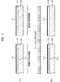
以下、図7〜図9の(A),(B)を参照して、本発明に係る表示装置の製造方法の実施形態を詳細に説明する。尚、図7〜図9の(A),(B)に示した工程図で、図中、左側の部分が画素TFT形成領域を表わし、右側が周辺TFT形成領域を表わしている。本実施形態においては、これら画素TFT形成領域及び周辺TFT形成領域の両領域に対し同時並列的に画素TFT及び周辺TFTを集積形成していく。
【0047】
まず、図7(A)に示すように、合成石英などの透明絶縁基板101上に、画素トランジスタ形成領域においては裏面からの戻り光が画素トランジスタに入射することを防ぐ目的で、WSiなどのシリサイド膜あるいは金属膜などからなる第1遮光膜13を、例えば200nmの厚みで形成する。
この後、SiO2などからなる第1層間絶縁膜115を基板101の全面にCVD法などで形成する。その上に、画素トランジスタ及び周辺トランジスタの活性層となる多結晶シリコン膜111をCVD法により形成する。このとき、多結晶シリコンの膜厚は20〜80nmの間に調整されることが望ましい。本実施形態では、多結晶シリコン膜111の厚みを40nm〜45nmに設定している。
【0048】
次に、図7(B)に示すように、多結晶シリコン膜111に、シリコンを主成分とする電気的に不活性な不純物を適量だけイオン注入することにより、均質な非晶質シリコン膜を得る。本実施形態では、TFTの活性層のエネルギー準位に影響を及ぼさない不活性な不純物としてSi+をイオンインプランテーション装置で打ち込んでいる。このときの注入量は、固相成長後に画素トランジスタにおいて所望の結晶粒径が得られるように調整している。本実施形態では、イオン注入量を4×10¹⁴atms/cm2として、固相成長後の多結晶シリコン膜の平均結晶粒径が100nm程度となるように調整している。尚、Si+イオンの加速エネルギーは30keV〜50keVに設定している。
【0049】
続いて、図8(A)に示すように画素トランジスタ形成領域をレジスト121などで被覆し、周辺トランジスタ形成領域にのみ前工程と同様にシリコンを主成分とする電気的に不活性な不純物を適量イオン注入する。このときの注入量と前工程での注入量との和が、固相成長後に周辺トランジスタにおいて所望の結晶粒径が得られるように調整される。本実施形態では、一回目の注入量と二回目の注入量との和が1.2×10¹⁵atms/cm2程度となるようにして、固相成長後の多結晶シリコン膜の平均結晶粒径が1000nmを超えるようにしている。このときの加速エネルギーは、一回目の注入と同様に30keV〜50keVである。このように、本実施形態では画素TFT形成領域にのみ選択的にレジストを形成する一方、シリコンイオンの打ち込みを二段階に分けることで、注入量を異ならせるようにしている。
【0050】
これに代えて、イオンインプランテーション装置で基板全面をスキャンしながらイオン注入を行なう際、画素TFT形成領域と周辺TFT形成領域とで注入量を異ならせるようにスキャニング制御を行なってもよい。あるいは、あらかじめ画素TFT形成領域にのみ薄く酸化膜を形成した後、基板全面に対して同一条件でイオン注入を行なうことも考えられる。この場合、画素TFT形成領域に照射されたシリコンイオンは一部が酸化膜に捕捉されるため、実質的な注入量は周辺TFT形成領域に比べ低くなる。このように、本発明は領域間で注入量を異ならせるため、種々の方策を採用することが可能である。
【0051】
続いて、レジスト121を剥離後、非晶質シリコン膜に600℃〜650℃程度の熱処理による固相成長を行なうことによって、多結晶シリコン膜を得ることができる。本実施例では、600℃程度に設定された炉に基板101を12時間投入することで、固相成長による再結晶化処理を行なっている。この結果、画素トランジスタ形成領域では平均的な粒径が100nm程度になった。一方、周辺トランジスタ形成領域では1000nm程度の多結晶シリコン膜111を同時に得ることができた。尚、場合によっては固相成長法に代え、エキシマレーザー光源などを用いたレーザー光照射によるアニールで、非晶質シリコンを多結晶シリコンに再結晶化してもよい。
【0052】
続いて、図8(B)に示すように、多結晶シリコン膜111をフォトリソグラフィ及びドライエッチング法で各トランジスタの素子領域の形状にパタニングする。その上にSiO2などからなるゲート絶縁膜125を介してゲート電極112を配置し、画素トランジスタ及び周辺トランジスタの基本的な構造を作り込む。この時、ゲート絶縁膜125の膜厚は80nm程度である。また、ゲート電極112は多結晶シリコンあるいはWSiなどのシリサイド化合物などが用いられる。
【0053】
続いて、図9(A)に示すように、SiO2などからなる第2層間絶縁膜116をCVD法により、例えば600nmの厚みで形成する。この第2層間絶縁膜116に対し、層間接続のためのコンタクトホールをドライエッチング法により形成した上で、配線119を形成する。画素TFTの側では、配線119はデータ配線を兼ねた第2遮光膜を含んでいる。このため、配線119は遮光性を備えたW、Al、Cu、Tiなどの金属あるいはシリサイド化合物の単層もしくは多層膜からなる。配線119の膜厚は一般的に400〜800nm程度である。配線119は、適宜設計に応じてフォトリソグラフィ及びドライエッチングによりパタニングされている。
【0054】
最後に、図9(B)に示すように、プラズマCVD法などによりSiO2からなる第3層間絶縁膜117を堆積する。更にCMP法(化学機械研磨法)などにより第3層間絶縁膜117の表面を平滑化する。ここで第3層間絶縁膜117に層間接続のためのコンタクトホールをドライエッチング法により形成した後、W,Ti,Cr,Alなどの金属あるいはシリサイド化合物などからなる第3遮光膜114を形成する。この第3遮光膜114は画素TFTを覆うように形成され、その膜厚は遮光するに十分な値を有している。例えば、Tiからなる第3遮光膜114の場合には、200nm以上の膜厚とすることが望ましい。更に第4層間絶縁膜118を介してITOなどの透明導電膜などからなる画素電極120を形成する。
【0055】
以上により、絶縁基板101の上に画素TFTと周辺TFTが同時に集積形成され、TFT基板が完成する。尚、この後図示しないが、TFT基板と対向基板を接合し、両者の間隔に液晶を注入することによって液晶表示装置が完成する。
【0056】
以上説明したように、本実施形態によれば、画素トランジスタの半導体薄膜の平均結晶粒径と周辺トランジスタの半導体薄膜の平均結晶粒径をそれぞれ別個に最適化している。これにより、従来と同じ開口率あるいは遮光構造を有する表示装置において、光リークに起因するフリッカ、ざらつき、コントラスト低下といった画品位の低下を各段に改善することが可能になった。
また、このような表示装置をプロジェクタに適用することで、LCDの入射光の許容量が拡大し、より明るく小型のプロジェクタを実現することができる。また、開口率を損なうことなく耐光性の改善を図ることが可能である。
【0057】
画素トランジスタと周辺トランジスタの活性層における多結晶シリコンを作り分けることによって、画素トランジスタに求められる低光リーク性と、周辺トランジスタに求められる高移動度を両立させることができる。本発明により、領域的に粒径の異なる多結晶シリコン膜を有するTFT基板を均質に且つ大量に製造することができる。
【0058】
なお、上述した実施形態において、画素トランジスタの半導体薄膜(活性層)の平均結晶粒径と周辺トランジスタの活性層(半導体薄膜)の平均結晶粒径をそれぞれ別個に最適化する方法として、Siイオンの注入量が異なるように行う方法を例に説明したが、本発明はこれに限定されるものではない。たとえば画素トランジスタと周辺トランジスタの活性層(半導体薄膜)の平均結晶粒径をそれぞれ別個に最適化する方法として、画素トランジスタと周辺トランジスタにおける非晶質シリコン層の厚さを変えておき、Siを固相成長させる第2の製造方法、あるいは、アモルファスシリコン(a−Si)から固相成長させる第3の製造方法を採用することができる。
【0059】
以下に、第2の製造方法と第3の製造方法について図面に関連付けて説明する。尚、以下の説明では、理解を容易にするために図7〜図9の(A),(B)と同一構成部分については同一符号を用いる。
【0060】
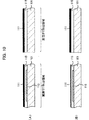
まず、図10及び図11の(A),(B)に関連付けて第2の製造方法について説明する。
まず、図10(A)に示すように、合成石英などの透明絶縁基板101上に、画素トランジスタ形成領域においては裏面からの戻り光が画素トランジスタに入射することを防ぐ目的で、WSiなどのシリサイド膜あるいは金属膜などからなる第1遮光膜13を、例えば200nmの厚みで形成する。
【0061】
この後、SiO2などからなる第1層間絶縁膜115を基板101の全面にCVD法などで形成する。
その上に、画素トランジスタ及び周辺トランジスタの活性層となる多結晶シリコン膜111をSiH4系の減圧CVD法により形成する。このとき、多結晶シリコンの膜厚はたとえば50nmに調整される。この場合、たとえば炉中の温度は約620°C、真空度は0.1Torr、SiH4は150sccmに設定される。
【0062】
次に、図10(B)に示すように、多結晶シリコン膜111の膜厚を、画素トランジスタにおける厚さが30nmとなり、周辺トランジスタの厚さは50nmに保持するように、たとえばフォトリソグラフィ及びドライエッチング法により選択的にパターニングする。たとえば平行平板型RIE装置を用いる。この場合、RFパワーが150W/cm2、真空度は0.2〜0.4Paに設定され、CL2ガスは180ml/min、O2ガスは6ml/minに流量が設定される。
【0063】
次に、図11(A)に示すように、多結晶シリコン膜111に、シリコンを主成分とする電気的に不活性な不純物を適量だけイオン注入することにより、均質な非晶質シリコン膜を得る。本実施形態では、TFTの活性層のエネルギー準位に影響を及ぼさない不活性な不純物としてSi+をイオンインプランテーション装置で打ち込んでいる。このときの注入量は、固相成長後に画素トランジスタにおいて所望の結晶粒径が得られるように調整している。この場合、たとえばイオン注入量が2×10¹⁵atms/cm2に設定され、Si+イオンの加速エネルギーは30keV〜50keV、好適には40にkeVに設定される。
【0064】
続いて、非晶質シリコン膜に対して熱処理による固相成長を行なうことによって、多結晶シリコン膜を得ることができる。この場合、N2ガス中において、温度600°Cの雰囲気下に24時間投入することで、固相成長による再結晶化処理を行なっている。その結果、画素TFT形成領域における固相成長後の平均結晶粒径が250nm程度となり、周辺TFT形成領域における固相成長後の平均結晶粒径が1500nm程度となった。
【0065】
続いて、図10(B)に示すように、多結晶シリコン膜111をフォトリソグラフィ及びドライエッチング法で各トランジスタの素子領域の形状にパタニングする。その上にSiO2などからなるゲート絶縁膜125を介してゲート電極112を配置し、画素トランジスタ及び周辺トランジスタの基本的な構造を作り込む。この時、ゲート絶縁膜125の膜厚は80nm程度である。また、ゲート電極112は多結晶シリコンあるいはWSiなどのシリサイド化合物などが用いられる。
【0066】
以降の工程は、図9(A),(B)の場合と同様に行われることから、ここではその詳細な説明は省略する。
次に、図12(A)〜(C)及び図13(A),(B)に関連付けて第3の製造方法について説明する。
【0067】
まず、図12(A)に示すように、合成石英などの透明絶縁基板101上に、画素トランジスタ形成領域においては裏面からの戻り光が画素トランジスタに入射することを防ぐ目的で、WSiなどのシリサイド膜あるいは金属膜などからなる第1遮光膜13を、例えば200nmの厚みで形成する。
この後、SiO2などからなる第1層間絶縁膜115を基板101の全面にCVD法などで形成する。
【0068】
その上に、画素トランジスタ及び周辺トランジスタの活性層となるa−Si膜111aをSi2H6系の減圧CVD法により形成する。このとき、a−si膜の膜厚はたとえば20nmに調整される。この場合、たとえば炉中の温度は約425°C、真空度は1.2Torr、Si2H6は300sccmに設定される。
【0069】
次に、図12(B)に示すように、画素トランジスタにおけるa−Si膜111aの膜厚を、周辺トランジスタの厚さは20nmに保持したままで、たとえばエッチングにより選択的に剥離する。たとえば平行平板型RIE装置を用いる。この場合、RFパワーが150W/cm2、真空度は0.2〜0.4Paに設定され、CL2ガスは180ml/min、O2ガスは6ml/minに流量が設定される。
【0070】
次に、たとえばHF系エッチャントで軽く自然酸化膜を剥離した後、図12(C)に示すように、画素トランジスタ及び周辺トランジスタの活性層となるa−Si膜111bをSi2H6系の減圧CVD法により形成する。このとき、a−si膜の膜厚はたとえば30nmに調整される。従って、画素TFT形成領域のa−si膜111bの膜厚はたとえば30nmとなり、周辺TFT形成領域のa−Si膜の膜厚111bは50nmとなる。この場合も、たとえば炉中の温度は約425°C、真空度は1.2Torr、Si2H6は300sccmに設定される。
【0071】
次に、図13(A)に示すように、a−Si膜111bに、シリコンを主成分とする電気的に不活性な不純物を適量だけイオン注入することにより、均質な非晶質シリコン膜を得る。本実施形態では、TFTの活性層のエネルギー準位に影響を及ぼさない不活性な不純物としてSi+をイオンインプランテーション装置で打ち込んでいる。このときの注入量は、固相成長後に画素トランジスタにおいて所望の結晶粒径が得られるように調整している。この場合、たとえばイオン注入量が5×10¹³atms/cm2に設定され、Si+イオンの加速エネルギーは30keV〜50keV、好適には40にkeVに設定される。
【0072】
続いて、非晶質シリコン膜に対して熱処理による固相成長を行なうことによって、多結晶シリコン膜を得ることができる。この場合、N2ガス中において、温度600°Cの雰囲気下に10〜30時間、好適には24時間投入することで、固相成長による再結晶化処理を行なっている。その結果、画素TFT形成領域における固相成長後の平均結晶粒径が200nm程度となり、周辺TFT形成領域における固相成長後の平均結晶粒径が1000nm程度となった。
【0073】
a−Si膜から固相成長する場合、核生成は膜中からより基板との界面、a−Si膜表面、若しくは2層成長させた場合には第1層と第2層との界面からが多い。この場合、膜厚を薄くすれば界面の効果が大きく平均結晶粒径は小さくなとものと考えられる。さらにa−Siの減圧CVD(LPCVD)による成膜においては、完全にアモルファス化しない極小領域が存在し、そこから核生成する場合がある。したがって、LPCVDによるa−Si膜に1×10¹²〜1015atms/cm2のイオン注入を行なうことができる。これは、微小な核を完全にアモルファス化するためである。特に、2層成長の場合には有効であり、この場合には、1×1013atms/cm2のイオン注入を行なうことが好ましい。
【0074】
勿論、LPCVD成長条件によってもこのような微小核領域は、形成しにくくなる。たとえばSiH4系においては、550°C弱、Si2H6系においては430°C弱が成長レートも考慮すると望ましい。
【0075】
続いて、図13(B)に示すように、多結晶シリコン膜111をフォトリソグラフィ及びドライエッチング法で各トランジスタの素子領域の形状にパタニングする。その上にSiO2などからなるゲート絶縁膜125を介してゲート電極112を配置し、画素トランジスタ及び周辺トランジスタの基本的な構造を作り込む。この時、ゲート絶縁膜125の膜厚は80nm程度である。また、ゲート電極112は多結晶シリコンあるいはWSiなどのシリサイド化合物などが用いられる。
【0076】
以降の工程は、図9(A),(B)の場合と同様に行われることから、ここではその詳細な説明は省略する。
なお、第2の製造方法において、a−Si系により形成して良く、また、第3の製造方法において、多結晶Si系で形成しても良い。
【0077】
また、ゲート酸化膜の形成工程は、SiH4のLPCVD法を採用しているが、通常の高温(熱)酸化でも勿論良い。その際の周辺TFT形成領域は、計80nm、画素TFT形成領域は50nm程度に、多結晶Si化し、酸化膜の厚さを調整する必要がある。この場合、たとえば周辺TFT形成領域における酸化膜の厚さは50nm、画素TFT形成領域の酸化膜の厚さは50nm、残った多結晶Si膜は、周辺TFT形成領域で55nm、画素TFT形成領域で25nmとなる。
【0078】
上記方法によって、実際には、画素TFT形成領域における活性層の平均粒径は150nm〜200nm、周辺TFT形成領域における活性層の平均粒径は2000〜2500nm程度が得られた。
【0079】
以上のように作製された表示装置は、上述したように、図2に示したプロジェクタのライトバルブ、すなわち液晶表示パネルとして用いることができるが、透過型の液晶表示パネルを3枚用いてカラー画像表示を行う、図14に示すようないわゆる3板方式プロジェクタにも適用することもできる。
【0080】
図14は、本実施形態に係る表示装置(液晶表示パネル)の応用例である3板方式プロジェクタ(投射型表示装置)の全体構成の一例を示す図である。
図14に示すプロジェクタ200は、透過型の液晶表示パネルを3枚用いてカラー画像表示を行ういわゆる3板方式のものであって、図14に示す液晶表示パネル225R,225G,225Bは、それぞれ図3及び図4の(A),(B)に示す構造を有している。
【0081】
プロジェクタは、光を出射する光源211と、一対の第1および第2レンズアレイ212,213と、第1および第2レンズアレイ212,213間に設けられ、光路(光軸210)を第2レンズアレイ213側に略90度曲げるように配置された全反射ミラー214とを備えている。第1および第2レンズアレイ212,213には、それぞれ複数のマイクロレンズ212M,213Mが2次元的に配列されている。第1および第2レンズアレイ212,213は、光の照度分布を均一化させるためのものであり、入射した光を複数の小光束に分割する機能を有している。
【0082】
光源211は、カラー画像表示に必要とされる、赤色光、青色光、緑色光を含んだ白色光を出射する。光源211は、白色光を発する図示しない発光体と、発光体から発せられた光を反射、集光する凹面鏡とを含んで構成される。発光体としては、例えば、ハロゲンランプ、メタルハライドランプまたはキセノンランプ等が使用される。凹面鏡は、集光効率が良い形状であることが望ましく、例えば回転楕円面鏡や回転放物面鏡等の回転対象な面形状となっている。
【0083】
第2レンズアレイ213の光の出射側に、PS合成素子215と、コンデンサレンズ216と、ダイクロイックミラー217とが順に配置されている。ダイクロイックミラー217は、入射した光を、例えば赤色光LRと、その他の色光とに分離する。
【0084】
PS合成素子215には、第2レンズアレイ213における隣り合うマイクロレンズ213M間に対応する位置に、複数の1/2波長板215Aが設けられている。PS合成素子215は、入射した光をP偏光成分およびS偏光成分の偏光光に分離する機能を有している。また、PS合成素子215は、分離された2つの偏光光のうち、一方の偏光光を、その偏光方向(例えば、P偏光)を保ったままPS合成素子215から出射し、他方の偏光光(例えば、S偏光)を、1/2波長板215Aの作用により、他の偏光成分(P偏光成分)に変換して出射する機能を有している。
【0085】
ダイクロイックミラー217によって分離された赤色光LRの光路に沿って、全反射ミラー218と、フィールドレンズ224Rと、液晶表示パネル225Rとが順に配置されている。全反射ミラー218は、ダイクロイックミラー217によって分離された赤色光LRを液晶表示パネル225Rに向けて反射する。液晶表示パネル225Rは、フィールドレンズ224Rを介して入射した赤色光LRを、画像信号に応じて空間的に変調する。
【0086】
ダイクロイックミラー217によって分離された他の色光の光路に沿って、ダイクロイックミラー219が設けられている。ダイクロイックミラー219は、入射した光を例えば緑色光LGと青色光LBとに分離する。
ダイクロイックミラー219によって分離された緑色光LGの光路に沿って、フィールドレンズ224Gと、液晶表示パネル225Gとが順に配置されている。液晶表示パネル225Gは、フィールドレンズ224Gを介して入射した緑色光LGを、画像信号に応じて空間的に変調する。
【0087】
ダイクロイックミラー219によって分離された青色光LBの光路に沿って、リレーレンズ220と、全反射ミラー221と、リレーレンズ222と、全反射ミラー223と、フィールドレンズ224Bと、液晶表示パネル225Bとが順に配置されている。全反射ミラー221は、リレーレンズ220を介して入射した青色光LBを、全反射ミラー223に向けて反射する。全反射ミラー223は、全反射ミラー221によって反射され、リレーレンズ222を介して入射した青色光LBを、液晶表示パネル225Bに向けて反射する。液晶表示パネル225Bは、全反射ミラー223によって反射され、フィールドレンズ224Bを介して入射した青色光LBを、画像信号に応じて空間的に変調する。
【0088】
赤色光LR、緑色光LGおよび青色光LBの光路が交わる位置に、3つの色光LR,LG,LBを合成する機能を有するクロスプリズム226が配置されている。また、クロスプリズム226から出射された合成光を、スクリーン228に向けて投射するための投射レンズ227が設けられている。
【0089】
クロスプリズム226は、3つの入射面226R,226G,226Bと、一つの出射面226Tとを有している。入射面226Rには、液晶表示パネル225Rから出射された赤色光LRが入射する。入射面226Gには、液晶表示パネル225Gから出射された緑色光LGが入射する。入射面226Bには、液晶表示パネル225Bから出射された青色光LBが入射する。クロスプリズム226は、入射面226R,226G,226Bに入射した3つの色光を合成して出射面226Tから出射する。
【0090】
本実施形態に係る液晶表示パネルを上記のような非常に強力な光源を用いるプロジェクタに適用した場合、高速駆動よりも高い耐光性が要求される画素トランジスタの活性層に光感度の低い多結晶あるいは非晶質の非単結晶シリコンを用い、回路特性上比較的光による誤動作に強く、耐光性よりも高速駆動が要求される駆動トランジスタの活性層に単結晶シリコンを用いていることから、耐光性と高速駆動とを両立させることができ、プロジェクタの表示品質を高めることができる。
【0091】
以上説明したように、本発明の表示装置およびその製造方法は、画素トランジスタと周辺トランジスタの活性層における多結晶シリコンを作り分けることによって、画素トランジスタに求められる低光リーク性と、周辺トランジスタに求められる高移動度を両立させることができることから、一般的な開口率あるいは遮光構造を有する液晶表示装置やプロジェクタに適用すること可能である。
【図面の簡単な説明】
【図1】 図1は、一般的なアクティブマトリクス型表示装置の全体構成を示す模式的な斜視図である。
【図2】 図2は、図1に示した液晶表示パネルを応用したプロジェクタの構成例を示す図である。
【図3】 図3は本発明に係る表示装置の一実施形態を示す模式図であって、図3(A)は表示パネルに形成される表示部及び駆動部の配置構成を示し、図3(B)はたとえば図3(A)のB−B線に沿って切断した表示パネルの断面構造を示している。
【図4】 図4(A)は画素トランジスタ(画素TFT:PXL−TFT)の断面構造を示す図であり、図4(B)は周辺トランジスタ(周辺TFT:PRP−TFT))の断面構造を示す図である。
【図5】 図5は、多結晶シリコンの平均粒径と、画素TFTの光リーク電流と周辺TFTのオン電流との関係を示すグラフである。
【図6】 図6はシリコンイオンの注入量と固相成長後の多結晶シリコンの平均粒径との関係を示すグラフである。
【図7】 図7(A),(B)は本発明に係る表示装置の第1の製造方法を示す工程図である。
【図8】 図8(A),(B)は本発明に係る表示装置の第1の製造方法を示す工程図である。
【図9】 図9(A),(B)は本発明に係る表示装置の第1の製造方法を示す工程図である。
【図10】 図10(A),(B)は本発明に係る表示装置の第2の製造方法を示す工程図である。
【図11】 図11(A),(B)は本発明に係る表示装置の第2の製造方法を示す工程図である。
【図12】 図12(A)〜(C)は本発明に係る表示装置の第3の製造方法を示す工程図である。
【図13】 図13(A),(B)は本発明に係る表示装置の第3の製造方法を示す工程図である。
【図14】 図14は、本実施形態に係る液晶表示パネルを適用した3板方式プロジェクタ(投射型表示装置)の全体構成の一例を示す図である。
【符号の説明】
100・・・表示パネル
101・・・ガラス基板
102・・・ガラス基板
103・・・シール材
104・・・液晶
105・・・表示部(DSP)
106L,106R・・・垂直駆動回路(VDRV)
107・・・水平駆動回路(HDRV)
111・・・多結晶シリコン膜
112・・・ゲート電極
113・・・第1遮光膜
114・・・第3遮光膜
115・・・第1層間絶縁膜
116・・・第2層間絶縁膜
117・・・第3層間絶縁膜
118・・・第4層間絶縁膜
119・・・配線(第2遮光膜を含む)
120・・・画素電極
20,200・・投射型表示装置(プロジェクタ)
211・・・光源
225R,225G,225B・・・液晶表示パネル
228・・・スクリーン[0001]
BACKGROUND OF THE INVENTION
The present invention relates to a flat display device represented by a liquid crystal display device (LCD), a manufacturing method thereof, and a projection display device. More specifically, the present invention relates to an active matrix display device in which a pixel array portion (display portion) having an active matrix configuration and a peripheral drive portion are integrally formed, a manufacturing method thereof, and a projection display device. More specifically, the present invention relates to a structure of a thin film transistor included in a display portion and a driving portion.
[0002]
[Prior art]
FIG. 1 is a schematic perspective view showing the overall configuration of a general active matrix display device.
[0003]
As shown in FIG. 1, the display device includes a
[0004]
The
[0005]
In the
[0006]
On the other hand, a counter electrode (not shown) is formed on the inner surface of the
[0007]
As described above, the TFT 14b is provided for each pixel, and switches each pixel between lighting and extinguishing. In this specification, the pixel switching TFT formed in the
[0008]
FIG. 2 is a diagram illustrating a configuration example of a projection display device (hereinafter referred to as a projector) to which the liquid
[0009]
As shown in FIG. 2, the
[0010]
The liquid
[0011]
As described above, a projection display device (projector) to which a liquid crystal display device (LCD) is applied is rapidly spreading along with improvement in brightness because a large screen display can be easily obtained.
The projector is a device that has a powerful light source, performs image control by an LCD serving as a light valve, and enlarges and projects image information, and powerful light is incident on the LCD. Due to the demand for further improvement in screen brightness or miniaturization for projectors, the amount of incident light per unit area for LCDs is increasing.
[0012]
On the other hand, the reflected light generated inside the optical system or the LCD due to strong incident light partially hits the active layer of the pixel transistor, so that the pixel transistor generates a leak current (hereinafter referred to as a light leak current) due to photoexcitation. The increase in the light leakage current causes flicker and screen roughness, and causes a fatal defect in image quality.
Conventionally, in order to cope with an increase in the amount of incident light, a light shielding structure for shielding the pixel transistor from above and below has been formed. A metal film or silicide film is arranged so as to cover the incident side and the emission side of the pixel transistor, and by optimizing the shape and size, the light to the pixel transistor is shielded, and the image quality is maintained or improved. Have worked hard.
[0013]
However, since the light shielding structure inevitably sacrifices the aperture ratio of the pixel, it conflicts with the demand for higher screen brightness. Due to the necessity of improving the aperture ratio of the LCD panel, it is already difficult to secure a sufficient light shielding area.
[0014]
[Problems to be solved by the invention]
An object of the present invention is to improve the light resistance of the pixel transistor itself without depending on the light shielding structure, that is, a display device capable of achieving both a high aperture ratio of the pixel and a high light resistance of the pixel transistor, and its manufacture A method and a projection display device are provided.
[0015]
[Means for Solving the Problems]
In order to achieve the above object, the following measures were taken. That is, a first aspect of the present invention includes a substrate on which a display unit and a peripheral drive unit are integrally formed, and the display unit includes pixels arranged in a matrix and between lighting / extinguishing of the pixels. The pixel transistors that switch in the above are formed in an integrated manner, and in the drive section, peripheral transistors constituting a drive circuit for scanning a matrix of pixel transistors are formed in an integrated manner. Any transistor1st and 2ndThrough the gate insulating film1st and 2ndPolycrystalGenderWith conductor thin film1st and 2ndA display device comprising a thin film transistor in which a gate electrode is laminated,The pixel transistor includes a first light shielding film formed with a certain width on a surface side of the substrate, a first interlayer insulating film formed so as to cover the substrate and the first light shielding film, and the first interlayer The first polycrystalline semiconductor thin film formed on the insulating film so as to face the first light shielding film across one edge and the other edge of the first light shielding film, and the first polycrystalline semiconductor A first gate electrode formed on the thin film via the first gate insulating film; and a second gate formed to cover the first interlayer insulating film, the first gate insulating film, and the first gate electrode. An interlayer insulating film and a first contact hole formed in the second interlayer insulating film are connected to a source region of the first polycrystalline semiconductor thin film, and the first gate electrode is formed on the second interlayer insulating film. From the edge of the source region side Via a first wiring as a second light-shielding film which is formed so as to be opposed over one edge of the polycrystalline semiconductor thin film and a second contact hole formed in the second interlayer insulating film Connected to the drain region of the first polycrystalline semiconductor thin film, on the second interlayer insulating film, from the edge of the drain region of the first gate electrode to the other edge of the first polycrystalline semiconductor thin film A second wiring as a second light-shielding film having a light-shielding property formed so as to face each other, and a third interlayer insulation formed so as to cover the second interlayer insulating film, the first wiring, and the second wiring A film and a fifth contact hole formed in the third interlayer insulating film and connected to the second wiring, and the one edge portion of the first polycrystalline semiconductor thin film on the third interlayer insulating film; To face across the other edge A third light-shielding film formed and having conductivity and connected to the pixel electrode, wherein the peripheral transistor includes the first interlayer insulating film formed on the substrate surface and the first interlayer insulating film. The second polycrystalline semiconductor thin film formed on the second polycrystalline semiconductor thin film, the second gate electrode formed on the second polycrystalline semiconductor thin film via the second gate insulating film, the first interlayer insulating film, The second polycrystallinity is formed through the second interlayer insulating film formed to cover the second gate insulating film and the second gate electrode, and the third contact hole formed in the second interlayer insulating film. Connected to the source region of the semiconductor thin film and facing the edge of the second gate electrode from the source region side to the edge of the second polycrystalline semiconductor thin film on the second interlayer insulating film Third wiring formed and the second interlayer insulation The fourth polycrystalline semiconductor thin film is connected to the drain region of the second polycrystalline semiconductor thin film through a fourth contact hole formed in the film, and is formed on the second interlayer insulating film from the edge side of the drain region of the second gate electrode. A fourth wiring formed so as to face across the other edge of the polycrystalline semiconductor thin film;,The third interlayer insulating film, the third interlayer insulating film formed so as to cover the third wiring and the fourth wiring,Of the pixel transistor1st polycrystallineAverage crystal grain size of semiconductor thin filmsBut,Of the peripheral transistorSecond polycrystallineAverage crystal grain size of semiconductor thin filmsSmaller thanIt is characterized by that.
[0016]
SpecificallyBeforeThe semiconductor thin film is polycrystalline silicon. The average crystal grain size of the polycrystalline silicon constituting the semiconductor thin film of the pixel transistor is 300 nm or less, and the average crystal grain size of the polycrystalline silicon constituting the semiconductor thin film of the peripheral transistor is 800 nm or more. The polycrystalline silicon has a thickness of 25 to 50 nm.
[0017]
According to a second aspect of the present invention, there is provided a substrate on which a display unit and a peripheral drive unit are integrally formed, and the display unit includes pixels arranged in a matrix and between turning on / off. The pixel transistors that switch in the above are formed in an integrated manner, and in the drive section, peripheral transistors constituting a drive circuit for scanning a matrix of pixel transistors are formed in an integrated manner. Each of the transistors is a method of manufacturing a display device including a thin film transistor having a polycrystalline silicon film as an active layer, and has a certain width in the pixel transistor formation region of the pixel transistor formation region and the peripheral transistor formation region on the substrate. A first film-forming step of forming a first light-shielding film, and the substrate and the display unit and the drive unit of the substrate A second film forming step of forming a first interlayer insulating film on the first light shielding film, and a second step of forming a polycrystalline silicon film on the first interlayer insulating film over the display unit and the driving unit of the substrate. (3) Ions that are once converted into an amorphous silicon film by ion implantation of inert ions that do not affect the electrical characteristics of the polycrystalline silicon film as an active layer into the polycrystalline silicon film An implantation step, and a recrystallization step for obtaining a polycrystalline silicon film again by heating the amorphous silicon film,Patterning the polycrystalline silicon film;The pixel transistor formation region and the peripheral transistor formation regionForming a first polycrystalline silicon film and a second polycrystalline silicon film respectivelyPatterning step and the pixel transistor formation regionofA fourth film forming step of forming a first gate electrode and a second gate electrode on the first polycrystalline silicon film and the second polycrystalline silicon film in the peripheral transistor formation region via a gate insulating film, respectively; The first gate electrode, the second gate electrode, the first polycrystalline silicon film, the second polycrystalline silicon film, and the substrate over the display unit and the driving unitSecondA fifth film forming step of forming a two interlayer insulating film; and the pixel transistor in the second interlayer insulating filmFormationFirst and second contact holes reaching the drain region and the source region of the first polycrystalline silicon film in the region, and the peripheral transistorFormationA first contact hole forming step of forming third and fourth contact holes reaching the source region and drain region of the second polycrystalline silicon film in the region;2The first wiring and the second wiring as the second light shielding film are formed on the second interlayer insulating film by being connected to the source region and the drain region of the first polycrystalline silicon film by contact holes, and 3rd and 3rd4A sixth film forming step of forming a third wiring and a fourth wiring connected to the source region and the drain region of the second polycrystalline silicon film by contact holes and reaching the second interlayer insulating film; A seventh film forming step of forming a third interlayer insulating film so as to cover the interlayer insulating film, the first wiring, the second wiring, the third wiring, and the fourth wiring; The pixel transistorFormationA second contact hole forming step of forming a fifth contact hole reaching the second wiring in the region, and connected to the second wiring through the fifth contact hole and reaching the third interlayer insulating filmRAn eighth film-forming step of forming a third light-shielding film that functions as a light-shielding film and is electrically conductive and connected to the pixel electrode. In the patterning step, the first polycrystalline silicon film is On the first interlayer insulating film, the first light shielding film is formed so as to face the first light shielding film between one edge and the other edge, and in the sixth film forming step, the first wiring On the second interlayer insulating film from the edge of the first gate electrode on the source region side to one edge of the first polycrystalline silicon film and function as a second light shielding film The second wiring is opposed to the second interlayer insulating film across the other edge of the first polycrystalline silicon film from the edge of the drain region of the first gate electrode, And formed so as to function as a second light-shielding film. The third light shielding film is formed on the third interlayer insulating film so as to oppose the one edge portion and the other edge portion of the first polycrystalline silicon film, and in the ion implantation step, the display The ion implantation amount is smaller in the portion than in the driving portion, so that the average crystal grain size of the first polycrystalline silicon film of the pixel transistor obtained in the recrystallization step is equal to that of the peripheral transistor. 2 It is characterized in that it is smaller than the average crystal grain size of the polycrystalline silicon film.
[0018]
Preferably, the recrystallization step is performed by a solid phase growth method in which the substrate is placed in a furnace set at 580 ° C. or higher in a nitrogen atmosphere and heat treatment is performed for a predetermined time. Alternatively, the recrystallization step is performed by a laser annealing method in which laser treatment is performed by irradiating the substrate with laser light. The ion implantation step is performed such that the display unit has a smaller ion implantation amount than the driving unit, and thus the average crystal of the polycrystalline silicon film of the pixel transistor obtained in the recrystallization step. The grain size is made smaller than the average crystal grain size of the polycrystalline silicon film of the peripheral transistor. In the recrystallization step, the average crystal grain size of the polycrystalline silicon film of the pixel transistor is 300 nm or less, and the average crystal grain size of the polycrystalline silicon film of the peripheral transistor is 800 nm or more. In the film forming step, the polycrystalline silicon film is formed in a thickness range of 25 to 50 nm.
[0019]
According to a third aspect of the present invention, there is provided a substrate on which a display unit and a peripheral drive unit are integrally formed, and the display unit includes pixels arranged in a matrix and between turning on / off. The pixel transistors that switch in the above are formed in an integrated manner, and in the drive section, peripheral transistors constituting a drive circuit for scanning a matrix of pixel transistors are formed in an integrated manner. Each of the transistors is a method of manufacturing a display device including a thin film transistor having a polycrystalline silicon film as an active layer, and has a certain width in the pixel transistor formation region of the pixel transistor formation region and the peripheral transistor formation region on the substrate. A first film-forming step of forming a first light-shielding film, and the substrate and the display unit and the drive unit of the substrate A second film forming step of forming a first interlayer insulating film on the first light shielding film, and a single crystal silicon film or polycrystalline silicon on the first interlayer insulating film over the display portion and the driving portion of the substrate A third film forming step for forming a film and injecting inactive ions that do not affect the electrical characteristics of the polycrystalline silicon film as the active layer into the polycrystalline silicon film once to form amorphous silicon An ion implantation step for converting into a film, a recrystallization step for obtaining a polycrystalline silicon film again by heat-treating the amorphous silicon film,Patterning the polycrystalline silicon film;The pixel transistor formation region and the peripheral transistor formation regionForming a first polycrystalline silicon film and a second polycrystalline silicon film respectivelyPatterning step and the pixel transistor formation regionofA fourth film forming step of forming a first gate electrode and a second gate electrode on the first polycrystalline silicon film and the second polycrystalline silicon film in the peripheral transistor formation region via a gate insulating film, respectively; The first gate electrode, the second gate electrode, the first polycrystalline silicon film, the second polycrystalline silicon film, and the substrate over the display unit and the driving unitSecondA fifth film forming step of forming a two interlayer insulating film; and the pixel transistor in the second interlayer insulating filmFormationFirst and second contact holes reaching the drain region and the source region of the first polycrystalline silicon film in the region, and the peripheral transistorFormationA first contact hole forming step of forming third and fourth contact holes reaching the source region and drain region of the second polycrystalline silicon film in the region;2The first wiring and the second wiring as the second light shielding film are formed on the second interlayer insulating film by being connected to the source region and the drain region of the first polycrystalline silicon film by contact holes, and 3rd and 3rd4A sixth film forming step of forming a third wiring and a fourth wiring connected to the source region and the drain region of the second polycrystalline silicon film by contact holes and reaching the second interlayer insulating film; A seventh film forming step of forming a third interlayer insulating film so as to cover the interlayer insulating film, the first wiring, the second wiring, the third wiring, and the fourth wiring; The pixel transistorFormationA second contact hole forming step of forming a fifth contact hole reaching the second wiring in the region, and connected to the second wiring through the fifth contact hole and reaching the third interlayer insulating filmRAn eighth film-forming step of forming a third light-shielding film that functions as a light-shielding film and is electrically conductive and connected to the pixel electrode. In the patterning step, the first polycrystalline silicon film is On the first interlayer insulating film, the first light shielding film is formed so as to face the first light shielding film between one edge and the other edge, and in the sixth film forming step, the first wiring On the second interlayer insulating film from the edge of the first gate electrode on the source region side to one edge of the first polycrystalline silicon film and function as a second light shielding film The second wiring is opposed to the second interlayer insulating film across the other edge of the first polycrystalline silicon film from the edge of the drain region of the first gate electrode, And formed so as to function as a second light-shielding film. Forming the third light-shielding film on the third interlayer insulating film so as to face the one edge portion of the first polycrystalline silicon film and the other edge portion; The first polycrystalline silicon constituting the active layer of the pixel transistor is formed so as to be thinner than the second polycrystalline silicon constituting the active layer of the peripheral transistor. The average crystal grain size of the first polycrystalline silicon film of the pixel transistor obtained in the crystallization step was made smaller than the average crystal grain size of the second polycrystalline silicon film of the peripheral transistor.
[0020]
Preferably, the third film forming step includes a first step of forming a single crystal silicon film or a polycrystalline silicon film to a first thickness over the display portion and the drive portion of the substrate, and And a second step of selectively removing the single crystal silicon film or the polycrystalline silicon film formed on the display portion to the second thickness. Preferably, the third film forming step includes a first step of forming a single crystal silicon film or a polycrystalline silicon film to a predetermined thickness over the display portion and the drive portion of the substrate, and the substrate. A second step of once removing the single crystal silicon film or the polycrystalline silicon film formed on the display portion, and further forming a single crystal silicon film or a polycrystalline silicon film over the display portion and the drive portion of the substrate. And a third step of forming a film.
[0021]
Further, a fourth aspect of the present invention is a projection display device that projects light formed on the display panel by irradiating light from a light source onto at least one display panel, and the display panel includes: A display unit and a peripheral driving unit are integrally formed on the substrate, and the display unit is integrally formed with pixels arranged in a matrix and pixel transistors that switch between turning on and off. In the driving unit, peripheral transistors constituting a driving circuit for scanning a matrix of pixel transistors are formed in an integrated manner, and both the pixel transistors and the peripheral transistors are formed.1st and 2ndThrough the gate insulating film1st and 2ndPolycrystalGenderWith conductor thin film1st and 2ndA display device comprising a thin film transistor in which a gate electrode is laminated,The pixel transistor includes a first light shielding film formed with a certain width on a surface side of the substrate, a first interlayer insulating film formed so as to cover the substrate and the first light shielding film, and the first interlayer The first polycrystalline semiconductor thin film formed on the insulating film so as to face the first light shielding film across one edge and the other edge of the first light shielding film, and the first polycrystalline semiconductor A first gate electrode formed on the thin film via the first gate insulating film; and a second gate formed to cover the first interlayer insulating film, the first gate insulating film, and the first gate electrode. An interlayer insulating film and a first contact hole formed in the second interlayer insulating film are connected to a source region of the first polycrystalline semiconductor thin film, and the first gate electrode is formed on the second interlayer insulating film. From the edge of the source region side Via a first wiring as a second light-shielding film which is formed so as to be opposed over one edge of the polycrystalline semiconductor thin film and a second contact hole formed in the second interlayer insulating film Connected to the drain region of the first polycrystalline semiconductor thin film, on the second interlayer insulating film, from the edge of the drain region of the first gate electrode to the other edge of the first polycrystalline semiconductor thin film A second wiring as a second light-shielding film having a light-shielding property formed so as to face each other, and a third interlayer insulation formed so as to cover the second interlayer insulating film, the first wiring, and the second wiring A film and a fifth contact hole formed in the third interlayer insulating film and connected to the second wiring, and the one edge portion of the first polycrystalline semiconductor thin film on the third interlayer insulating film; To face across the other edge A third light-shielding film formed and having conductivity and connected to the pixel electrode, wherein the peripheral transistor includes the first interlayer insulating film formed on the substrate surface and the first interlayer insulating film. The second polycrystalline semiconductor thin film formed on the second polycrystalline semiconductor thin film, the second gate electrode formed on the second polycrystalline semiconductor thin film via the second gate insulating film, the first interlayer insulating film, The second polycrystallinity is formed through the second interlayer insulating film formed to cover the second gate insulating film and the second gate electrode, and the third contact hole formed in the second interlayer insulating film. Connected to the source region of the semiconductor thin film and facing the edge of the second gate electrode from the source region side to the edge of the second polycrystalline semiconductor thin film on the second interlayer insulating film Third wiring formed and the second interlayer insulation The fourth polycrystalline semiconductor thin film is connected to the drain region of the second polycrystalline semiconductor thin film through a fourth contact hole formed in the film, and is formed on the second interlayer insulating film from the edge side of the drain region of the second gate electrode. A fourth wiring formed so as to face across the other edge of the polycrystalline semiconductor thin film;,The third interlayer insulating film, the third interlayer insulating film formed so as to cover the third wiring and the fourth wiring,Of the pixel transistor1st polycrystallineAverage crystal grain size of semiconductor thin filmsBut,Of the peripheral transistorSecond polycrystallineAverage crystal grain size of semiconductor thin filmsSmaller thanYes.
[0022]
According to the present invention, by optimizing the crystal grain size of the polycrystalline silicon film of the pixel transistor and the polycrystalline silicon film of the peripheral drive circuit transistor, the light resistance of the pixel transistor can be improved in each stage, and The electrical characteristics of the transistor can be maintained well. Specifically, the light leakage current can be suppressed by controlling the average crystal grain size of the polycrystalline silicon film serving as the active layer of the pixel transistor to be relatively small. The smaller the crystal grain size, the more crystal defects. It is considered that the carriers excited by light irradiation are quickly captured by the defect level, resulting in an increase in the off-resistance of the transistor, thereby suppressing an increase in light leakage current. On the other hand, the average crystal grain size of the polycrystalline silicon film constituting the peripheral transistor is controlled to be relatively large. As the crystal grain size increases, the carrier mobility increases and the driving capability of the peripheral transistor increases. Compared with the pixel transistor, the peripheral transistor is required to operate at high speed for pixel scanning and image signal sampling. In the present invention, the drive capability of peripheral transistors is ensured to maintain image quality.
[0023]
【The invention's effect】
According to the present invention, the light resistance of the pixel transistor itself is improved without depending on the light shielding structure, that is, the high aperture ratio of the pixel and the high light resistance of the pixel transistor can be compatible.
[0024]
DETAILED DESCRIPTION OF THE INVENTION
Hereinafter, embodiments of the present invention will be described in detail with reference to the drawings.
FIG. 3 is a schematic view showing an embodiment of a display device according to the present invention. FIG. 3A shows an arrangement configuration of a display portion and a drive portion formed on the display panel, and FIG. For example, a cross-sectional structure of a display panel cut along line BB in FIG.
[0025]
As shown in the figure, the
[0026]
In this display device, as shown in FIG. 1A, a display portion (DSP) 105 and a peripheral driving portion are integrally formed on a
[0027]
The
[0028]
The
The peripheral drive unit including the vertical drive circuits (VDRV) 106L and 106R, the horizontal drive circuit (HDRV) 107, and the
[0029]
As a feature of the present invention, the average crystal grain size of the semiconductor thin film of the pixel transistor is different from the average crystal grain size of the semiconductor thin film of the peripheral transistor. Specifically, the average crystal grain size of the semiconductor thin film of the pixel transistor is smaller than the average crystal grain size of the semiconductor thin film of the peripheral transistor. As the semiconductor thin film, polycrystalline silicon is mainly used. In this case, the average crystal grain size of the polycrystalline silicon constituting the semiconductor thin film of the pixel transistor is controlled to 300 nm or less, and the average crystal grain size of the polycrystalline silicon constituting the semiconductor thin film of the peripheral transistor is controlled to 800 nm or more. The film thickness of the polycrystalline silicon is controlled to 25 to 50 nm.
[0030]
4A is a diagram illustrating a cross-sectional structure of a pixel transistor (pixel TFT: PXL-TFT), and FIG. 4B is a diagram illustrating a cross-sectional structure of a peripheral transistor (peripheral TFT: PRP-TFT). .
In the pixel transistor, a first light-shielding
[0031]
As described above, the pixel TFT basically has a stacked structure in which the
[0032]
In the peripheral TFT, as shown in FIG. 4B, a
[0033]
The peripheral TFTs are formed in parallel with the pixel TFTs, and basically have the same layer configuration. However, unlike the pixel TFT, the peripheral TFT does not require a high degree of light shielding, so the first
[0034]
The pixel TFT and the peripheral TFT shown in FIGS. 4A and 4B are basically manufactured in parallel by a film forming process, an ion implantation process, and a recrystallization process.
In the film forming process, the
[0035]
As a feature of the present invention, the ion implantation process is performed such that, for example, the display unit and the driving unit have different ion implantation amounts, and thus the polycrystalline silicon film of the pixel TFT obtained by the recrystallization process.111Average crystal grain size and polycrystalline silicon film of peripheral TFT111The average crystal grain size is different.
[0036]
The recrystallization process is performed in a furnace set at 600 ° C. or higher in a nitrogen atmosphere.101In accordance with a solid phase growth method in which a heat treatment is performed for a predetermined time. Alternatively, the recrystallization step may employ a laser annealing method in which the substrate is irradiated with laser light such as excimer laser light and heat treatment is performed.
[0037]
The ion implantation process is performed, for example, so that the amount of ion implantation in the display unit is smaller than that in the peripheral driving unit, so that the average crystal grain size of the polycrystalline silicon film of the pixel TFT obtained in the recrystallization process is The average crystal grain size of the polycrystalline silicon film of the transistor is made smaller. Preferably, the recrystallization step is adjusted so that the average crystal grain size of the
[0038]
FIG. 5 is a graph showing the relationship between the average grain size of polycrystalline silicon, the light leakage current of the pixel TFT, and the on-current of the peripheral TFT. In FIG. 5, the horizontal axis represents the average grain size (grain size) GS of the polycrystalline silicon, the left vertical axis in the figure represents the light leakage current ILK of the pixel TFT, and the right vertical axis in the figure represents the on-state of the peripheral TFT. Each current ION is represented. In addition, the curve indicated by L in the figure shows the characteristics of the light leakage current of the pixel TFT with respect to the average grain size of polycrystalline silicon, and the curve indicated with O shows the characteristics of the on-current of peripheral TFTs with respect to the average grain diameter of polycrystalline silicon. Yes. Note that the measurement was performed under light irradiation with a gate-source voltage Vgs of the pixel TFT and peripheral TFTs Vgs = −6 V and a drain-source voltage Vds = 10 V. In this case, the light is irradiated with an ultra-high pressure mercury lamp (for example, UHP lamp (manufactured by Philips) or metal halide lamp), and about 3000 to 5000 lx is irradiated on the transistor. In addition, an infrared (IR) cut filter is installed, and unnecessary light is measured under the condition of cutting.
[0039]
As shown in FIG. 5, the light leakage current of the pixel TFT increases as the average grain size of the polycrystalline silicon increases. Also, the on-current of the peripheral TFT increases as the average grain size of the polycrystalline silicon increases. Based on these relationships, in this embodiment, the average crystal grain sizes of the polycrystalline silicon of the pixel transistor and the polycrystalline silicon of the peripheral transistor are made different and optimized.
[0040]
Experiments have confirmed that the leakage current during light irradiation can be suppressed by reducing the grain size of polycrystalline silicon. Part of the incident light that has become stray light easily hits the channel portion of the pixel TFT due to reflection in the optical system, multiple reflection in the LCD, or diffraction. This increases the light leakage current of the pixel transistor, which adversely affects image quality. In order to maintain image quality, the leakage current during light irradiation needs to be controlled to 2 pA or less in the case of an LCD that writes frame image information on the display unit at a refresh rate of 60 Hz, for example. Preferably, it is controlled to around 1 pA or less.
[0041]
Such a content forms an LCD panel having an active layer of a pixel transistor corresponding to the grain size, and is an actual device of a commercially available three-plate projector, or a commercially available three-plate projector optical irradiation as shown in FIG. This is an optical projection system close to the conditions, and the result of visual observation of the image quality by projecting and irradiating on a screen in a dark room was obtained.
Therefore, as shown in the graph of FIG. 5, by controlling the grain size of polycrystalline silicon to 300 nm or less, the leakage current of the pixel TFT is sufficiently 2 pA or less, preferably around 1 pA or less, even during light irradiation. It is possible to suppress it.
[0042]
On the other hand, a TFT having an active layer made of polycrystalline silicon having a small particle size has a lower driving ability than a TFT having an active layer made of polycrystalline silicon having a large particle size. Peripheral TFTs may be sufficiently shielded by parting panels due to the structure of the panel. From the operational characteristics, transistor characteristics with higher carrier mobility and higher on-current value are desired than low light leakage current. Yes.
Therefore, in this embodiment, as shown in FIG. 5, the average grain size of the polycrystalline silicon of the peripheral TFT is controlled to 800 nm or more at which the on-current ION of the peripheral TFT starts to saturate to obtain desired operating characteristics. Yes. This gives 5 × 10 white light7An LCD having both high light resistance and good image quality that can handle an incident light amount corresponding to (lx) can be obtained.
[0043]
FIG. 6 is a graph showing the relationship between the amount of implanted silicon ions and the average grain size of polycrystalline silicon after solid phase growth. In FIG. 6, the horizontal axis represents the Si ion implantation amount (Si · ion · AMT), and the vertical axis represents the grain size GSAG of the polycrystalline Si after solid phase growth.
As is apparent from the figure, the grain size of the polycrystalline silicon after recrystallization increases as the amount of implanted silicon ions increases. For example, the silicon ion implantation amount is 4.0 × 10¹⁴atms / cm2In this case, the average grain size of polycrystalline silicon is about 100 nm. On the other hand, the implantation amount of silicon ions is 1.2 × 10¹⁵atms / cm2Then, the average crystal grain size of polycrystalline silicon reaches 1000 nm, and depending on conditions, it may reach about 2000 nm.
[0044]
When silicon ions are implanted, the polycrystalline structure at the time of film formation is destroyed and once becomes an amorphous structure. At that time, a part that becomes a nucleus in the recrystallization in the subsequent step is also left. If the amount of silicon ions implanted is small, more parts are left as nuclei. Therefore, when recrystallization treatment is performed in a later step, crystal growth starts around each nucleus, and the crystal grains come into contact with each other in a relatively short time, and the individual crystal grain size itself is small. Stop on. On the other hand, the density of the remaining nuclei decreases as the amount of silicon ions implanted increases to bring it closer to the amorphous state. As a result, in the subsequent recrystallization process, crystals can sufficiently grow around individual nuclei, and a relatively large particle size can be obtained. However, when silicon ions are excessively implanted, the film becomes completely amorphous and no nuclei remain.
[0045]
The present embodiment utilizes this phenomenon, and as a first method, the ion implantation process is performed so that the amount of ion implantation in the display unit is smaller than that in the driving unit, and thus is obtained in the recrystallization process. The average crystal grain size of the crystal silicon film of the pixel transistor is controlled to be smaller than the average crystal grain size of the polycrystalline silicon film of the peripheral transistor.
[0046]
Hereinafter, an embodiment of a method for manufacturing a display device according to the present invention will be described in detail with reference to FIGS. In FIGS. 7A to 9B, the left side represents the pixel TFT formation region, and the right side represents the peripheral TFT formation region. In the present embodiment, pixel TFTs and peripheral TFTs are integrated and formed simultaneously in parallel in both the pixel TFT formation region and the peripheral TFT formation region.
[0047]
First, as shown in FIG. 7A, a silicide such as WSi is formed on a transparent insulating
After this, SiO2A first
[0048]
Next, as shown in FIG. 7B, a homogeneous amorphous silicon film is formed by ion-implanting an appropriate amount of electrically inactive impurities mainly composed of silicon into the
[0049]
Subsequently, as shown in FIG. 8A, the pixel transistor formation region is covered with a resist 121 or the like, and an appropriate amount of electrically inactive impurities mainly composed of silicon is applied only to the peripheral transistor formation region as in the previous step. Ion implantation. The sum of the implantation amount at this time and the implantation amount in the previous step is adjusted so that a desired crystal grain size can be obtained in the peripheral transistor after solid phase growth. In the present embodiment, the sum of the first injection amount and the second injection amount is 1.2 × 10 6.15atms / cm2The average crystal grain size of the polycrystalline silicon film after the solid phase growth is made to exceed 1000 nm. The acceleration energy at this time is 30 keV to 50 keV as in the first implantation. As described above, in this embodiment, the resist is selectively formed only in the pixel TFT formation region, while the implantation amount is made different by dividing the implantation of silicon ions into two stages.
[0050]
Alternatively, when ion implantation is performed while scanning the entire surface of the substrate with an ion implantation apparatus, scanning control may be performed so that the implantation amount differs between the pixel TFT formation region and the peripheral TFT formation region. Alternatively, it is conceivable that after a thin oxide film is formed only in the pixel TFT formation region in advance, ion implantation is performed on the entire surface of the substrate under the same conditions. In this case, since a part of silicon ions irradiated to the pixel TFT formation region is captured by the oxide film, the substantial implantation amount is lower than that of the peripheral TFT formation region. As described above, in the present invention, various measures can be adopted to vary the injection amount between regions.
[0051]
Subsequently, after removing the resist 121, a polycrystalline silicon film can be obtained by performing solid phase growth on the amorphous silicon film by heat treatment at about 600 ° C. to 650 ° C. In this embodiment, the
[0052]
Subsequently, as shown in FIG. 8B, the
[0053]
Subsequently, as shown in FIG.2A second
[0054]
Finally, as shown in FIG. 9B, the SiO 2 film is formed by plasma CVD or the like.2A third
[0055]
As described above, the pixel TFT and the peripheral TFT are simultaneously formed on the insulating
[0056]
As described above, according to the present embodiment, the average crystal grain size of the semiconductor thin film of the pixel transistor and the average crystal grain size of the semiconductor thin film of the peripheral transistor are optimized separately. As a result, in a display device having the same aperture ratio or light shielding structure as in the prior art, it has become possible to improve image quality degradation such as flicker, roughness, and contrast degradation due to light leakage.
Further, by applying such a display device to a projector, the allowable amount of incident light of the LCD is expanded, and a brighter and smaller projector can be realized. In addition, it is possible to improve light resistance without impairing the aperture ratio.
[0057]
By separately forming polycrystalline silicon in the active layers of the pixel transistor and the peripheral transistor, it is possible to achieve both low light leakage required for the pixel transistor and high mobility required for the peripheral transistor. According to the present invention, it is possible to manufacture a TFT substrate having a polycrystalline silicon film having different grain sizes in a uniform and large quantity.
[0058]
In the embodiment described above, as a method of optimizing the average crystal grain size of the semiconductor thin film (active layer) of the pixel transistor and the average crystal grain size of the active layer (semiconductor thin film) of the peripheral transistor, respectively, Although the method of performing the injection amount differently has been described as an example, the present invention is not limited to this. For example, as a method of individually optimizing the average crystal grain size of the active layer (semiconductor thin film) of the pixel transistor and the peripheral transistor, the thickness of the amorphous silicon layer in the pixel transistor and the peripheral transistor is changed, and Si is fixed. A second manufacturing method for phase growth or a third manufacturing method for solid phase growth from amorphous silicon (a-Si) can be employed.
[0059]
Hereinafter, the second manufacturing method and the third manufacturing method will be described with reference to the drawings. In the following description, the same reference numerals are used for the same components as those in FIGS. 7 to 9 in order to facilitate understanding.
[0060]
First, the second manufacturing method will be described with reference to FIGS. 10 and 11 (A) and (B).
First, as shown in FIG. 10A, a silicide such as WSi is formed on a transparent insulating
[0061]
After this, SiO2A first
On top of this, a
[0062]
Next, as shown in FIG. 10B, the thickness of the
[0063]
Next, as shown in FIG. 11A, a homogeneous amorphous silicon film is formed by ion-implanting an appropriate amount of electrically inactive impurities mainly composed of silicon into the
[0064]
Subsequently, a polycrystalline silicon film can be obtained by performing solid phase growth by heat treatment on the amorphous silicon film. In this case, N2A recrystallization process by solid phase growth is performed by introducing the gas in an atmosphere at a temperature of 600 ° C. for 24 hours. As a result, the average crystal grain size after solid phase growth in the pixel TFT formation region was about 250 nm, and the average crystal grain size after solid phase growth in the peripheral TFT formation region was about 1500 nm.
[0065]
Subsequently, as shown in FIG. 10B, the
[0066]
Since the subsequent steps are performed in the same manner as in FIGS. 9A and 9B, detailed description thereof is omitted here.
Next, a third manufacturing method will be described with reference to FIGS. 12 (A) to 12 (C) and FIGS. 13 (A) and 13 (B).
[0067]
First, as shown in FIG. 12A, a silicide such as WSi is formed on a transparent insulating
After this, SiO2A first
[0068]
On top of this, an
[0069]
Next, as shown in FIG. 12B, the
[0070]
Next, after the natural oxide film is lightly peeled off by using, for example, an HF-based etchant, as shown in FIG.2H6It is formed by a low pressure CVD method. At this time, the film thickness of the a-si film is adjusted to 30 nm, for example. Accordingly, the film thickness of the
[0071]
Next, as shown in FIG. 13A, a homogeneous amorphous silicon film is formed by ion-implanting an appropriate amount of electrically inactive impurities mainly composed of silicon into the
[0072]
Subsequently, a polycrystalline silicon film can be obtained by performing solid phase growth by heat treatment on the amorphous silicon film. In this case, N2In a gas, recrystallization treatment by solid phase growth is performed by introducing the gas in an atmosphere of 600 ° C. for 10 to 30 hours, preferably 24 hours. As a result, the average crystal grain size after solid phase growth in the pixel TFT formation region was about 200 nm, and the average crystal grain size after solid phase growth in the peripheral TFT formation region was about 1000 nm.
[0073]
When solid phase growth is performed from an a-Si film, nucleation occurs from the interface with the substrate, from the surface of the a-Si film, or when two layers are grown, from the interface between the first layer and the second layer. Many. In this case, it is considered that if the film thickness is reduced, the interface effect is large and the average crystal grain size is small. Furthermore, in the film formation by low pressure CVD (LPCVD) of a-Si, there is a minimal region that does not become completely amorphous, and nucleation may occur from there. Therefore, the LPCVD a-Si film is 1 × 10¹²-1015atms / cm2Ion implantation can be performed. This is in order to make minute nuclei completely amorphous. In particular, it is effective in the case of two-layer growth, and in this case, 1 × 10¹³atms / cm2It is preferable to perform ion implantation.
[0074]
Of course, it is difficult to form such a micronucleus region even under LPCVD growth conditions. For example, SiHFourIn the system, a little less than 550 ° C, Si2H6In the system, it is desirable that the temperature is slightly below 430 ° C. in consideration of the growth rate.
[0075]
Subsequently, as shown in FIG. 13B, the
[0076]
Since the subsequent steps are performed in the same manner as in FIGS. 9A and 9B, detailed description thereof is omitted here.
In the second manufacturing method, an a-Si system may be used, and in the third manufacturing method, a polycrystalline Si system may be used.
[0077]
In addition, the gate oxide film forming process is performed using SiH.FourThe LPCVD method is employed, but of course, normal high temperature (thermal) oxidation may be used. In that case, it is necessary to change the thickness of the oxide film by forming polycrystalline Si into a peripheral TFT formation region of about 80 nm and a pixel TFT formation region of about 50 nm. In this case, for example, the thickness of the oxide film in the peripheral TFT formation region is 50 nm, the thickness of the oxide film in the pixel TFT formation region is 50 nm, and the remaining polycrystalline Si film is 55 nm in the peripheral TFT formation region and in the pixel TFT formation region. 25 nm.
[0078]
In practice, the average particle size of the active layer in the pixel TFT formation region was about 150 nm to 200 nm, and the average particle size of the active layer in the peripheral TFT formation region was actually about 2000 to 2500 nm.
[0079]
As described above, the display device manufactured as described above can be used as the light valve of the projector shown in FIG. 2, that is, a liquid crystal display panel. However, a color image using three transmissive liquid crystal display panels is used. It can also be applied to a so-called three-plate projector as shown in FIG.
[0080]
FIG. 14 is a diagram illustrating an example of the overall configuration of a three-plate projector (projection display device) that is an application example of the display device (liquid crystal display panel) according to the present embodiment.
A
[0081]
The projector is provided between a
[0082]
The
[0083]
On the light exit side of the
[0084]
The
[0085]
A
[0086]
A
A
[0087]
A
[0088]
A
[0089]
The
[0090]
When the liquid crystal display panel according to the present embodiment is applied to a projector using a very powerful light source as described above, a polycrystal having low photosensitivity in an active layer of a pixel transistor that requires higher light resistance than high-speed driving or Because it uses amorphous non-single-crystal silicon, it is relatively resistant to light malfunction due to circuit characteristics, and single-crystal silicon is used for the active layer of the drive transistor that requires high-speed driving rather than light resistance. And high-speed driving can be achieved, and the display quality of the projector can be improved.
[0091]
As described above, the display device and the manufacturing method thereof according to the present invention require low light leakage required for the pixel transistor and the peripheral transistor by separately forming polycrystalline silicon in the active layer of the pixel transistor and the peripheral transistor. Therefore, the present invention can be applied to a liquid crystal display device or a projector having a general aperture ratio or a light shielding structure.
[Brief description of the drawings]
FIG. 1 is a schematic perspective view showing an overall configuration of a general active matrix display device.
FIG. 2 is a diagram showing a configuration example of a projector to which the liquid crystal display panel shown in FIG. 1 is applied.
3 is a schematic view showing an embodiment of a display device according to the present invention. FIG. 3A shows an arrangement configuration of a display portion and a drive portion formed on the display panel. FIG. 3B shows a cross-sectional structure of the display panel cut along the line BB in FIG.
4A is a diagram showing a cross-sectional structure of a pixel transistor (pixel TFT: PXL-TFT), and FIG. 4B is a cross-sectional structure of a peripheral transistor (peripheral TFT: PRP-TFT). FIG.
FIG. 5 is a graph showing the relationship between the average grain size of polycrystalline silicon, the light leakage current of the pixel TFT, and the on-current of the peripheral TFT.
FIG. 6 is a graph showing the relationship between the amount of implanted silicon ions and the average grain size of polycrystalline silicon after solid phase growth.
7A and 7B are process diagrams showing a first method for manufacturing a display device according to the present invention.
8A and 8B are process diagrams showing a first method for manufacturing a display device according to the present invention.
FIGS. 9A and 9B are process diagrams showing a first method for manufacturing a display device according to the present invention. FIGS.
FIGS. 10A and 10B are process diagrams showing a second method for manufacturing a display device according to the present invention. FIGS.
11A and 11B are process diagrams showing a second manufacturing method of the display device according to the present invention.
FIGS. 12A to 12C are process diagrams showing a third method for manufacturing a display device according to the present invention. FIGS.
13A and 13B are process diagrams showing a third method for manufacturing a display device according to the present invention.
FIG. 14 is a diagram illustrating an example of an overall configuration of a three-plate projector (projection display device) to which the liquid crystal display panel according to the present embodiment is applied.
[Explanation of symbols]
100 ... Display panel
101 ... Glass substrate
102 ... Glass substrate
103 ... Sealing material
104 ... Liquid crystal
105 ... Display unit (DSP)
106L, 106R ... Vertical drive circuit (VDRV)
107 ... Horizontal drive circuit (HDRV)
111... Polycrystalline silicon film
112 ... Gate electrode
113 ... 1st light shielding film
114... Third light shielding film
115... First interlayer insulating film
116: Second interlayer insulating film
117... Third interlayer insulating film
118: Fourth interlayer insulating film
119... Wiring (including second light shielding film)
120... Pixel electrode
20,200 ・ ・ Projection type display device (projector)
211 ... Light source
225R, 225G, 225B ... Liquid crystal display panel
228 ... Screen
Claims (20)
前記表示部は、マトリクス状に配置された画素と、これを点灯/消灯の間でスイッチングする画素トランジスタとが集積的に形成されており、
前記駆動部は、画素トランジスタのマトリクスを走査するための駆動回路を構成する周辺トランジスタが集積的に形成されており、
前記画素トランジスタ及び周辺トランジスタはいずれも第1及び第2ゲート絶縁膜を介して第1及び第2多結晶性半導体薄膜と第1及び第2ゲート電極を積層した薄膜トランジスタからなる表示装置であって、
前記画素トランジスタは、
前記基板の表面側に一定の幅をもって形成された第1遮光膜と、
前記基板および前記第1遮光膜を覆うように形成された第1層間絶縁膜と、
前記第1層間絶縁膜上に、前記第1遮光膜の一縁部と他縁部間にわたって当該第1遮光膜と対向するように形成された前記第1多結晶性半導体薄膜と、
前記第1多結晶性半導体薄膜上に前記第1ゲート絶縁膜を介して形成された前記第1ゲート電極と、
前記第1層間絶縁膜、前記第1ゲート絶縁膜および前記第1ゲート電極を覆うように形成された第2層間絶縁膜と、
前記第2層間絶縁膜に形成された第1コンタクトホールを介して前記第1多結晶性半導体薄膜のソース領域に接続され、前記第2層間絶縁膜上において前記第1ゲート電極のソース領域側の縁部側から前記第1多結晶性半導体薄膜の一縁部に亘って対向するように形成され遮光性を有する第2遮光膜としての第1配線と、
前記第2層間絶縁膜に形成された第2コンタクトホールを介して前記第1多結晶性半導体薄膜のドレイン領域に接続され、前記第2層間絶縁膜上において前記第1ゲート電極のドレイン領域の縁部側から前記第1多結晶性半導体薄膜の前記他縁部に亘って対向するように形成され遮光性を有する第2遮光膜としての第2配線と、
前記第2層間絶縁膜、前記第1配線および前記第2配線を覆うように形成された第3層間絶縁膜と、
前記第3層間絶縁膜に形成された第5コンタクトホールを介して前記第2配線に接続され、前記第3層間絶縁膜上において前記第1多結晶性半導体薄膜の前記一縁部と前記他縁部に亘って対向するように形成され、導電性を有し画素電極と接続される第3遮光膜と、を含み、
前記周辺トランジスタは、
前記基板表面に形成された前記第1層間絶縁膜と、
前記第1層間絶縁膜上に形成された前記第2多結晶性半導体薄膜と、
前記第2多結晶性半導体薄膜上に前記第2ゲート絶縁膜を介して形成された前記第2ゲート電極と、
前記第1層間絶縁膜、前記第2ゲート絶縁膜及び前記第2ゲート電極を覆うように形成された前記第2層間絶縁膜と、
前記第2層間絶縁膜に形成された第3コンタクトホールを介して前記第2多結晶性半導体薄膜のソース領域に接続され、前記第2層間絶縁膜上において前記第2ゲート電極のソース領域側の縁部側から前記第2多結晶性半導体薄膜の一縁部に亘って対向するように形成された第3配線と、
前記第2層間絶縁膜に形成された第4コンタクトホールを介して前記第2多結晶性半導体薄膜のドレイン領域に接続され、前記第2層間絶縁膜上において前記第2ゲート電極のドレイン領域の縁部側から前記第2多結晶性半導体薄膜の前記他縁部に亘って対向するように形成された第4配線と、
前記第2層間絶縁膜、前記第3配線および前記第4配線を覆うように形成された前記第3層間絶縁膜と、を含み、
前記画素トランジスタの第1多結晶性半導体薄膜の平均結晶粒径が、前記周辺トランジスタの第2多結晶性半導体薄膜の平均結晶粒径よりも小さい
表示装置。Comprising a substrate on which a display unit and a peripheral driving unit are integrally formed;
In the display unit, pixels arranged in a matrix and pixel transistors that switch between lighting and extinguishing are formed in an integrated manner.
In the drive unit, peripheral transistors constituting a drive circuit for scanning a matrix of pixel transistors are formed in an integrated manner.
Each of the pixel transistor and the peripheral transistor is a display device comprising a thin film transistor in which first and second polycrystalline semiconductor thin films and first and second gate electrodes are stacked via first and second gate insulating films,
The pixel transistor is
A first light-shielding film formed on the surface side of the substrate with a certain width;
A first interlayer insulating film formed to cover the substrate and the first light shielding film;
The first polycrystalline semiconductor thin film formed on the first interlayer insulating film so as to face the first light shielding film across one edge and the other edge of the first light shielding film;
The first gate electrode formed on the first polycrystalline semiconductor thin film via the first gate insulating film;
A second interlayer insulating film formed to cover the first interlayer insulating film, the first gate insulating film and the first gate electrode;
Connected to the source region of the first polycrystalline semiconductor thin film through a first contact hole formed in the second interlayer insulating film, and on the source region side of the first gate electrode on the second interlayer insulating film A first wiring as a second light-shielding film that is formed so as to face from one edge to the other edge of the first polycrystalline semiconductor thin film;
Connected to the drain region of the first polycrystalline semiconductor thin film through a second contact hole formed in the second interlayer insulating film, and on the second interlayer insulating film, the edge of the drain region of the first gate electrode A second wiring as a second light-shielding film that is formed so as to face the other edge portion of the first polycrystalline semiconductor thin film from the portion side and has a light-shielding property;
A third interlayer insulating film formed to cover the second interlayer insulating film, the first wiring, and the second wiring;
Connected to the second wiring through a fifth contact hole formed in the third interlayer insulating film, and the one edge portion and the other edge of the first polycrystalline semiconductor thin film on the third interlayer insulating film A third light-shielding film that is formed so as to be opposed across the portion and has conductivity and is connected to the pixel electrode,
The peripheral transistor is
The first interlayer insulating film formed on the substrate surface;
The second polycrystalline semiconductor thin film formed on the first interlayer insulating film;
The second gate electrode formed on the second polycrystalline semiconductor thin film via the second gate insulating film;
The second interlayer insulating film formed to cover the first interlayer insulating film, the second gate insulating film, and the second gate electrode;
Connected to the source region of the second polycrystalline semiconductor thin film through a third contact hole formed in the second interlayer insulating film, on the source region side of the second gate electrode on the second interlayer insulating film A third wiring formed so as to face from one edge to the other edge of the second polycrystalline semiconductor thin film;
Connected to the drain region of the second polycrystalline semiconductor thin film through a fourth contact hole formed in the second interlayer insulating film, and on the edge of the drain region of the second gate electrode on the second interlayer insulating film A fourth wiring formed so as to face the other edge portion of the second polycrystalline semiconductor thin film from the portion side;
The third interlayer insulating film, the third interlayer insulating film formed so as to cover the third wiring and the fourth wiring,
The average crystal grain size of the first polycrystalline semiconductor thin film of the pixel transistor is smaller than the average crystal grain size of the second polycrystalline semiconductor thin film of the peripheral transistor.
請求項1に記載の表示装置。The display device according to claim 1, wherein the first and second polycrystalline semiconductor thin films are polycrystalline silicon.
請求項2に記載の表示装置。The average crystal grain size of the polycrystalline silicon constituting the first polycrystalline semiconductor thin film of the pixel transistor is 300 nm or less, and the average crystal grain of the polycrystalline silicon constituting the second polycrystalline semiconductor thin film of the peripheral transistor The display device according to claim 2, wherein the diameter is 800 nm or more.
請求項2または3に記載の表示装置。The display device according to claim 2, wherein the polycrystalline silicon has a thickness of 25 to 50 nm.
請求項2または3に記載の表示装置。The film thickness of the polycrystalline silicon constituting the first polycrystalline semiconductor thin film of the pixel transistor is thinner than the thickness of the polycrystalline silicon constituting the second polycrystalline semiconductor thin film of the peripheral transistor. 3. The display device according to 3.
前記表示部は、マトリクス状に配置された画素と、これを点灯/消灯の間でスイッチングする画素トランジスタとが集積的に形成されており、前記駆動部は、画素トランジスタのマトリクスを走査するための駆動回路を構成する周辺トランジスタが集積的に形成されており、前記画素トランジスタ及び周辺トランジスタはいずれも多結晶シリコン膜を活性層とする薄膜トランジスタからなる表示装置の製造方法であって、
基板上の画素トランジスタ形成領域及び周辺トランジスタ形成領域のうち、前記画素トランジスタ形成領域において、一定の幅をもって第1遮光膜を形成する第1成膜工程と、
前記基板の表示部及び駆動部に亘って、前記基板及び前記第1遮光膜上に第1層間絶縁膜を形成する第2成膜工程と、
前記基板の表示部及び駆動部に亘って、前記第1層間絶縁膜上に多結晶シリコン膜を形成する第3成膜工程と、
活性層としての多結晶シリコン膜の電気的な特性に影響を及ぼさない不活性なイオンを前記多結晶シリコン膜にイオン注入することにより一旦非晶質シリコン膜に転換するイオン注入工程と、
この非晶質シリコン膜を加熱処理することによって再び多結晶シリコン膜を得る再結晶化工程と、
前記多結晶シリコン膜をパタニングして、前記画素トランジスタ形成領域及び周辺トランジスタ形成領域にそれぞれ第1多結晶シリコン膜及び第2多結晶シリコン膜を形成するパタニング工程と、
前記画素トランジスタ形成領域の第1多結晶シリコン膜及び周辺トランジスタ形成領域の第2多結晶シリコン膜上に、それぞれゲート絶縁膜を介して第1ゲート電極及び第2ゲート電極を形成する第4成膜工程と、
前記基板の表示部及び駆動部に亘って、前記第1ゲート電極、第2ゲート電極、第1多結晶シリコン膜、第2多結晶シリコン膜、基板上に第2層間絶縁膜を形成する第5成膜工程と、
前記第2層間絶縁膜に、前記画素トランジスタ形成領域における前記第1多結晶シリコン膜のソース領域、ドレイン領域に達する第1及び第2コンタクトホール、並びに、前記周辺トランジスタ形成領域における前記第2多結晶シリコン膜のソース領域、ドレイン領域に達する第3及び第4コンタクトホールを形成する第1コンタクトホール形成工程と、
前記第1及び第2コンタクトホールにより前記第1多結晶シリコン膜の前記ソース領域及びドレイン領域に接続させて前記第2層間絶縁膜上に至り第2遮光膜としての第1配線及び第2配線を形成し、かつ、前記第3及び第4コンタクトホールにより前記第2多結晶シリコン膜の前記ソース領域及びドレイン領域に接続させて前記第2層間絶縁膜上に至る第3配線及び第4配線を形成する第6成膜工程と、
前記第2層間絶縁膜、前記第1配線、前記第2配線、前記第3配線、及び前記第4配線を覆うように第3層間絶縁膜を形成する第7成膜工程と、
前記第3層間絶縁膜に、前記画素トランジスタ形成領域の前記第2配線に達する第5コンタクトホールを形成する第2コンタクトホール形成工程と、
前記第5コンタクトホールを介して前記第2配線に接続され、前記第3層間絶縁膜上に至り遮光膜として機能し、かつ導電性を有し画素電極と接続される第3遮光膜を形成する第8成膜工程と、を含み、
前記パタニング工程では、
前記第1多結晶シリコン膜を、前記第1層間絶縁膜上において、前記第1遮光膜の一縁部と他縁部間に亘って当該第1遮光膜と対向するように形成し、
前記第6成膜工程では、
前記第1配線を、前記第2層間絶縁膜上において前記第1ゲート電極のソース領域側の縁部側から前記第1多結晶シリコン膜の一縁部に亘って対向し、かつ、第2遮光膜として機能するように形成し、
前記第2配線を、前記第2層間絶縁膜上において前記第1ゲート電極のドレイン領域の縁部側から前記第1多結晶シリコン膜の前記他縁部に亘って対向し、かつ、第2遮光膜として機能するように形成し、
前記第8成膜工程では、
前記第3遮光膜を、前記第3層間絶縁膜上において前記第1多結晶シリコン膜の前記一縁部と前記他縁部に亘って対向するように形成し、
前記イオン注入工程では、
前記表示部の方が前記駆動部よりもイオン注入量が少なくなるように行ない、
もって、前記再結晶化工程で得られる前記画素トランジスタの第1多結晶シリコン膜の平均結晶粒径が前記周辺トランジスタの第2多結晶シリコン膜の平均結晶粒径より小さくなるようにした
表示装置の製造方法。Comprising a substrate on which a display unit and a peripheral driving unit are integrally formed;
The display unit is formed by integrally forming pixels arranged in a matrix and pixel transistors that switch between switching on and off, and the driving unit scans a matrix of pixel transistors. Peripheral transistors constituting a driving circuit are formed in an integrated manner, and both the pixel transistor and the peripheral transistor are a method for manufacturing a display device including a thin film transistor having a polycrystalline silicon film as an active layer,
A first film forming step of forming a first light-shielding film with a certain width in the pixel transistor formation region of the pixel transistor formation region and the peripheral transistor formation region on the substrate;
A second film forming step of forming a first interlayer insulating film on the substrate and the first light shielding film over the display unit and the driving unit of the substrate;
A third film forming step of forming a polycrystalline silicon film on the first interlayer insulating film over the display unit and the driving unit of the substrate;
An ion implantation step of once converting the amorphous silicon film into an amorphous silicon film by ion-implanting inert ions that do not affect the electrical characteristics of the polycrystalline silicon film as the active layer;
A recrystallization step of obtaining a polycrystalline silicon film again by heat-treating the amorphous silicon film;
Patterning the polycrystalline silicon film to form a first polycrystalline silicon film and a second polycrystalline silicon film in the pixel transistor formation region and the peripheral transistor formation region , respectively ;
A fourth film is formed by forming a first gate electrode and a second gate electrode on the first polycrystalline silicon film in the pixel transistor formation region and the second polycrystalline silicon film in the peripheral transistor formation region via a gate insulating film, respectively. Process,
Over the display portion and a driving portion of the substrate, the first gate electrode, the second gate electrode, a first polycrystalline silicon film, the second polycrystalline silicon film, a fifth of a second interlayer insulating film on a substrate A film forming process;
In the second interlayer insulating film, a source region and a second contact hole reaching the drain region of the first polycrystalline silicon film in the pixel transistor formation region, and the second polycrystal in the peripheral transistor formation region A first contact hole forming step of forming third and fourth contact holes reaching the source region and the drain region of the silicon film;
First and second lines of the second light-blocking film leads to the first and second co contact hole by the first polysilicon film and the source region and be connected to a drain region on the second interlayer insulating film forming a, and the third and fourth co contact hole by the second said source third wiring region and be connected to the drain region extending over the second interlayer insulating film and the fourth wiring polycrystalline silicon film A sixth film forming step for forming
A seventh film forming step of forming a third interlayer insulating film so as to cover the second interlayer insulating film, the first wiring, the second wiring, the third wiring, and the fourth wiring;
A second contact hole forming step of forming a fifth contact hole reaching the second wiring in the pixel transistor formation region in the third interlayer insulating film;
Forming a third light-shielding film the fifth is connected to the second wiring through a contact hole, is connected to the upper in the third interlayer insulating film functions as optimum Ri shielding film and the pixel electrode has conductivity And an eighth film forming step.
In the patterning process,
Forming the first polycrystalline silicon film on the first interlayer insulating film so as to face the first light shielding film across one edge and the other edge of the first light shielding film;
In the sixth film forming step,
The first wiring is opposed on the second interlayer insulating film from the edge of the first gate electrode on the source region side to one edge of the first polycrystalline silicon film, and the second light shielding. Formed to function as a film,
The second wiring is opposed on the second interlayer insulating film from the edge of the drain region of the first gate electrode to the other edge of the first polycrystalline silicon film, and a second light shielding Formed to function as a film,
In the eighth film forming step,
Forming the third light-shielding film on the third interlayer insulating film so as to face the one edge and the other edge of the first polycrystalline silicon film;
In the ion implantation step,
The display unit is performed so that the ion implantation amount is smaller than that of the driving unit,
Therefore, the average crystal grain size of the first polycrystalline silicon film of the pixel transistor obtained in the recrystallization step is made smaller than the average crystal grain size of the second polycrystalline silicon film of the peripheral transistor. Production method.
請求項6に記載の表示装置の製造方法。The method for manufacturing a display device according to claim 6, wherein the recrystallization step is performed by a solid phase growth method in which the substrate is placed in a furnace set at 580 ° C. or higher in a nitrogen atmosphere and heat treatment is performed for a predetermined time.
請求項6に記載の表示装置の製造方法。The method for manufacturing a display device according to claim 6, wherein the recrystallization step is performed by a laser annealing method in which the substrate is irradiated with laser light to perform heat treatment.
請求項6から8のいずれか一に記載の表示装置の製造方法。9. The recrystallization step, wherein the average crystal grain size of the polycrystalline silicon film of the pixel transistor is 300 nm or less, and the average crystal grain size of the polycrystalline silicon film of the peripheral transistor is 800 nm or more. A method for manufacturing the display device according to claim 1.
請求項6から9のいずれか一に記載の表示装置の製造方法。The method for manufacturing a display device according to claim 6, wherein in the third film formation step, the polycrystalline silicon film is formed in a thickness range of 25 to 50 nm.
前記表示部は、マトリクス状に配置された画素と、これを点灯/消灯の間でスイッチングする画素トランジスタとが集積的に形成されており、前記駆動部は、画素トランジスタのマトリクスを走査するための駆動回路を構成する周辺トランジスタが集積的に形成されており、前記画素トランジスタ及び周辺トランジスタはいずれも多結晶シリコン膜を活性層とする薄膜トランジスタからなる表示装置の製造方法であって、
基板上の画素トランジスタ形成領域及び周辺トランジスタ形成領域のうち、前記画素トランジスタ形成領域において、一定の幅をもって第1遮光膜を形成する第1成膜工程と、
前記基板の表示部及び駆動部に亘って、前記基板及び前記第1遮光膜上に第1層間絶縁膜を形成する第2成膜工程と、
前記基板の表示部及び駆動部に亘って、前記第1層間絶縁膜上に単結晶シリコン膜または多結晶シリコン膜を形成する第3成膜工程と、
活性層としての多結晶シリコン膜の電気的な特性に影響を及ぼさない不活性なイオンを前記多結晶シリコン膜にイオン注入することにより一旦非晶質シリコン膜に転換するイオン注入工程と、
この非晶質シリコン膜を加熱処理することによって再び多結晶シリコン膜を得る再結晶化工程と、
前記多結晶シリコン膜をパタニングして、前記画素トランジスタ形成領域及び周辺トランジスタ形成領域にそれぞれ第1多結晶シリコン膜及び第2多結晶シリコン膜を形成するパタニング工程と、
前記画素トランジスタ形成領域の第1多結晶シリコン膜及び周辺トランジスタ形成領域の第2多結晶シリコン膜上に、それぞれゲート絶縁膜を介して第1ゲート電極及び第2ゲート電極を形成する第4成膜工程と、
前記基板の表示部及び駆動部に亘って、前記第1ゲート電極、第2ゲート電極、第1多結晶シリコン膜、第2多結晶シリコン膜、基板上に第2層間絶縁膜を形成する第5成膜工程と、
前記第2層間絶縁膜に、前記画素トランジスタ形成領域における前記第1多結晶シリコン膜のソース領域、ドレイン領域に達する第1及び第2コンタクトホール、並びに、前記周辺トランジスタ形成領域における前記第2多結晶シリコン膜のソース領域、ドレイン領域に達する第3及び第4コンタクトホールを形成する第1コンタクトホール形成工程と、
前記第1及び第2コンタクトホールにより前記第1多結晶シリコン膜の前記ソース領域及びドレイン領域に接続させて前記第2層間絶縁膜上に至り第2遮光膜としての第1配線及び第2配線を形成し、かつ、前記第3及び第4コンタクトホールにより前記第2多結晶シリコン膜の前記ソース領域及びドレイン領域に接続させて前記第2層間絶縁膜上に至る第3配線及び第4配線を形成する第6成膜工程と、
前記第2層間絶縁膜、前記第1配線、前記第2配線、前記第3配線、及び前記第4配線を覆うように第3層間絶縁膜を形成する第7成膜工程と、
前記第3層間絶縁膜に、前記画素トランジスタ形成領域の前記第2配線に達する第5コンタクトホールを形成する第2コンタクトホール形成工程と、
前記第5コンタクトホールを介して前記第2配線に接続され、前記第3層間絶縁膜上に至り遮光膜として機能し、かつ導電性を有し画素電極と接続される第3遮光膜を形成する第8成膜工程と、を含み、
前記パタニング工程では、
前記第1多結晶シリコン膜を、前記第1層間絶縁膜上において、前記第1遮光膜の一縁部と他縁部間に亘って当該第1遮光膜と対向するように形成し、
前記第6成膜工程では、
前記第1配線を、前記第2層間絶縁膜上において前記第1ゲート電極のソース領域側の縁部側から前記第1多結晶シリコン膜の一縁部に亘って対向し、かつ、第2遮光膜として機能するように形成し、
前記第2配線を、前記第2層間絶縁膜上において前記第1ゲート電極のドレイン領域の縁部側から前記第1多結晶シリコン膜の前記他縁部に亘って対向し、かつ、第2遮光膜として機能するように形成し、
前記第8成膜工程では、
前記第3遮光膜を、前記第3層間絶縁膜上において前記第1多結晶シリコン膜の前記一縁部と前記他縁部に亘って対向するように形成し、
前記第3成膜工程は、
前記画素トランジスタの活性層を構成する第1多結晶シリコンの膜厚が、前記周辺トランジスタの活性層を構成する第2多結晶シリコンの膜厚より薄くなるように成膜を行ない、
もって、前記再結晶化工程で得られる前記画素トランジスタの第1多結晶シリコン膜の平均結晶粒径が前記周辺トランジスタの第2多結晶シリコン膜の平均結晶粒径より小さくなるようにした
表示装置の製造方法。Comprising a substrate on which a display unit and a peripheral driving unit are integrally formed;
The display unit is formed by integrally forming pixels arranged in a matrix and pixel transistors that switch between switching on and off, and the driving unit scans a matrix of pixel transistors. Peripheral transistors constituting a driving circuit are formed in an integrated manner, and both the pixel transistor and the peripheral transistor are a method for manufacturing a display device including a thin film transistor having a polycrystalline silicon film as an active layer,
A first film forming step of forming a first light-shielding film with a certain width in the pixel transistor formation region of the pixel transistor formation region and the peripheral transistor formation region on the substrate;
A second film forming step of forming a first interlayer insulating film on the substrate and the first light shielding film over the display unit and the driving unit of the substrate;
A third film forming step of forming a single crystal silicon film or a polycrystalline silicon film on the first interlayer insulating film over the display portion and the drive portion of the substrate;
An ion implantation step of once converting the amorphous silicon film into an amorphous silicon film by ion-implanting inert ions that do not affect the electrical characteristics of the polycrystalline silicon film as the active layer;
A recrystallization step of obtaining a polycrystalline silicon film again by heat-treating the amorphous silicon film;
Patterning the polycrystalline silicon film to form a first polycrystalline silicon film and a second polycrystalline silicon film in the pixel transistor formation region and the peripheral transistor formation region , respectively ;
A fourth film is formed by forming a first gate electrode and a second gate electrode on the first polycrystalline silicon film in the pixel transistor formation region and the second polycrystalline silicon film in the peripheral transistor formation region via a gate insulating film, respectively. Process,
Over the display portion and a driving portion of the substrate, the first gate electrode, the second gate electrode, a first polycrystalline silicon film, the second polycrystalline silicon film, a fifth of a second interlayer insulating film on a substrate A film forming process;
In the second interlayer insulating film, a source region and a second contact hole reaching the drain region of the first polycrystalline silicon film in the pixel transistor formation region, and the second polycrystal in the peripheral transistor formation region A first contact hole forming step of forming third and fourth contact holes reaching the source region and the drain region of the silicon film;
First and second lines of the second light-blocking film leads to the first and second co contact hole by the first polysilicon film and the source region and be connected to a drain region on the second interlayer insulating film forming a, and the third and fourth co contact hole by the second said source third wiring region and be connected to the drain region extending over the second interlayer insulating film and the fourth wiring polycrystalline silicon film A sixth film forming step for forming
A seventh film forming step of forming a third interlayer insulating film so as to cover the second interlayer insulating film, the first wiring, the second wiring, the third wiring, and the fourth wiring;
A second contact hole forming step of forming a fifth contact hole reaching the second wiring in the pixel transistor formation region in the third interlayer insulating film;
Forming a third light-shielding film the fifth is connected to the second wiring through a contact hole, is connected to the upper in the third interlayer insulating film functions as optimum Ri shielding film and the pixel electrode has conductivity And an eighth film forming step.
In the patterning process,
Forming the first polycrystalline silicon film on the first interlayer insulating film so as to face the first light shielding film across one edge and the other edge of the first light shielding film;
In the sixth film forming step,
The first wiring is opposed on the second interlayer insulating film from the edge of the first gate electrode on the source region side to one edge of the first polycrystalline silicon film, and the second light shielding. Formed to function as a film,
The second wiring is opposed on the second interlayer insulating film from the edge of the drain region of the first gate electrode to the other edge of the first polycrystalline silicon film, and a second light shielding Formed to function as a film,
In the eighth film forming step,
Forming the third light-shielding film on the third interlayer insulating film so as to face the one edge and the other edge of the first polycrystalline silicon film;
The third film forming step includes
Forming a film so that the thickness of the first polycrystalline silicon constituting the active layer of the pixel transistor is smaller than the thickness of the second polycrystalline silicon constituting the active layer of the peripheral transistor;
Therefore, the average crystal grain size of the first polycrystalline silicon film of the pixel transistor obtained in the recrystallization step is made smaller than the average crystal grain size of the second polycrystalline silicon film of the peripheral transistor. Production method.
前記基板の表示部に成膜された単結晶シリコン膜または多結晶シリコン膜を第2の厚さまで選択的に除去する第2の工程と、を含む
請求項11に記載の表示装置の製造方法。The third film forming step includes a first step of forming a single crystal silicon film or a polycrystalline silicon film to a first thickness over the display portion and the drive portion of the substrate,
The method for manufacturing a display device according to claim 11, further comprising: a second step of selectively removing the single crystal silicon film or the polycrystalline silicon film formed on the display portion of the substrate to a second thickness.
前記基板の表示部に成膜された単結晶シリコン膜または多結晶シリコン膜を一旦除去する第2の工程と、
前記基板の表示部及び駆動部に亘って単結晶シリコン膜または多結晶シリコン膜をさらに成膜する第3の工程と、を含む
請求項11に記載の表示装置の製造方法。The third film forming step includes a first step of forming a single crystal silicon film or a polycrystalline silicon film to a predetermined thickness over the display portion and the drive portion of the substrate,
A second step of temporarily removing the single crystal silicon film or the polycrystalline silicon film formed on the display portion of the substrate;
The method for manufacturing a display device according to claim 11, further comprising: a third step of forming a single crystal silicon film or a polycrystalline silicon film over the display portion and the drive portion of the substrate.
請求項11から13のいずれか一に記載の表示装置の製造方法。14. The solid-phase growth method according to claim 11, wherein the recrystallization step is performed by a solid phase growth method in which the substrate is placed in a furnace set at 580 ° C. or higher in a nitrogen atmosphere and heat treatment is performed for a predetermined time. Manufacturing method of display device.
請求項11から14のいずれか一に記載の表示装置の製造方法。15. The recrystallization step includes setting the average crystal grain size of the polycrystalline silicon film of the pixel transistor to 300 nm or less and the average crystal grain size of the polycrystalline silicon film of the peripheral transistor to 800 nm or more. A method for manufacturing the display device according to claim 1.
前記表示パネルは、
表示部及び周辺の駆動部が一体的に形成された基板を備え、
前記表示部は、マトリクス状に配置された画素と、これを点灯/消灯の間でスイッチングする画素トランジスタとが集積的に形成されており、
前記駆動部は、画素トランジスタのマトリクスを走査するための駆動回路を構成する周辺トランジスタが集積的に形成されており、
前記画素トランジスタ及び周辺トランジスタはいずれも第1及び第2ゲート絶縁膜を介して第1及び第2多結晶性半導体薄膜と第1及び第2ゲート電極を積層した薄膜トランジスタからなる表示装置であって、
前記画素トランジスタは、
前記基板の表面側に一定の幅をもって形成された第1遮光膜と、
前記基板および前記第1遮光膜を覆うように形成された第1層間絶縁膜と、
前記第1層間絶縁膜上に、前記第1遮光膜の一縁部と他縁部間にわたって当該第1遮光膜と対向するように形成された前記第1多結晶性半導体薄膜と、
前記第1多結晶性半導体薄膜上に前記第1ゲート絶縁膜を介して形成された前記第1ゲート電極と、
前記第1層間絶縁膜、前記第1ゲート絶縁膜および前記第1ゲート電極を覆うように形成された第2層間絶縁膜と、
前記第2層間絶縁膜に形成された第1コンタクトホールを介して前記第1多結晶性半導体薄膜のソース領域に接続され、前記第2層間絶縁膜上において前記第1ゲート電極のソース領域側の縁部側から前記第1多結晶性半導体薄膜の一縁部に亘って対向するように形成され遮光性を有する第2遮光膜としての第1配線と、
前記第2層間絶縁膜に形成された第2コンタクトホールを介して前記第1多結晶性半導体薄膜のドレイン領域に接続され、前記第2層間絶縁膜上において前記第1ゲート電極のドレイン領域の縁部側から前記第1多結晶性半導体薄膜の前記他縁部に亘って対向するように形成され遮光性を有する第2遮光膜としての第2配線と、
前記第2層間絶縁膜、前記第1配線および前記第2配線を覆うように形成された第3層間絶縁膜と、
前記第3層間絶縁膜に形成された第5コンタクトホールを介して前記第2配線に接続され、前記第3層間絶縁膜上において前記第1多結晶性半導体薄膜の前記一縁部と前記他縁部に亘って対向するように形成され、導電性を有し画素電極と接続される第3遮光膜と、を含み、
前記周辺トランジスタは、
前記基板表面に形成された前記第1層間絶縁膜と、
前記第1層間絶縁膜上に形成された前記第2多結晶性半導体薄膜と、
前記第2多結晶性半導体薄膜上に前記第2ゲート絶縁膜を介して形成された前記第2ゲート電極と、
前記第1層間絶縁膜、前記第2ゲート絶縁膜及び前記第2ゲート電極を覆うように形成された前記第2層間絶縁膜と、
前記第2層間絶縁膜に形成された第3コンタクトホールを介して前記第2多結晶性半導体薄膜のソース領域に接続され、前記第2層間絶縁膜上において前記第2ゲート電極のソース領域側の縁部側から前記第2多結晶性半導体薄膜の一縁部に亘って対向するように形成された第3配線と、
前記第2層間絶縁膜に形成された第4コンタクトホールを介して前記第2多結晶性半導体薄膜のドレイン領域に接続され、前記第2層間絶縁膜上において前記第2ゲート電極のドレイン領域の縁部側から前記第2多結晶性半導体薄膜の前記他縁部に亘って対向するように形成された第4配線と、
前記第2層間絶縁膜、前記第3配線および前記第4配線を覆うように形成された前記第3層間絶縁膜と、を含み、
前記画素トランジスタの第1多結晶性半導体薄膜の平均結晶粒径が、前記周辺トランジスタの第2多結晶性半導体薄膜の平均結晶粒径よりも小さい
投射型表示装置。A projection display device that irradiates at least one display panel with light from a light source and projects an image formed by the display panel on a screen,
The display panel is
Comprising a substrate on which a display unit and a peripheral driving unit are integrally formed;
In the display unit, pixels arranged in a matrix and pixel transistors that switch between lighting and extinguishing are formed in an integrated manner.
In the drive unit, peripheral transistors constituting a drive circuit for scanning a matrix of pixel transistors are formed in an integrated manner.
Each of the pixel transistor and the peripheral transistor is a display device comprising a thin film transistor in which first and second polycrystalline semiconductor thin films and first and second gate electrodes are stacked via first and second gate insulating films,
The pixel transistor is
A first light-shielding film formed on the surface side of the substrate with a certain width;
A first interlayer insulating film formed to cover the substrate and the first light shielding film;
The first polycrystalline semiconductor thin film formed on the first interlayer insulating film so as to face the first light shielding film across one edge and the other edge of the first light shielding film;
The first gate electrode formed on the first polycrystalline semiconductor thin film via the first gate insulating film;
A second interlayer insulating film formed to cover the first interlayer insulating film, the first gate insulating film and the first gate electrode;
Connected to the source region of the first polycrystalline semiconductor thin film through a first contact hole formed in the second interlayer insulating film, and on the source region side of the first gate electrode on the second interlayer insulating film A first wiring as a second light-shielding film that is formed so as to face from one edge to the other edge of the first polycrystalline semiconductor thin film;
Connected to the drain region of the first polycrystalline semiconductor thin film through a second contact hole formed in the second interlayer insulating film, and on the second interlayer insulating film, the edge of the drain region of the first gate electrode A second wiring as a second light-shielding film that is formed so as to face the other edge portion of the first polycrystalline semiconductor thin film from the portion side and has a light-shielding property;
A third interlayer insulating film formed to cover the second interlayer insulating film, the first wiring, and the second wiring;
Connected to the second wiring through a fifth contact hole formed in the third interlayer insulating film, and the one edge portion and the other edge of the first polycrystalline semiconductor thin film on the third interlayer insulating film A third light-shielding film that is formed so as to be opposed across the portion and has conductivity and is connected to the pixel electrode,
The peripheral transistor is
The first interlayer insulating film formed on the substrate surface;
The second polycrystalline semiconductor thin film formed on the first interlayer insulating film;
The second gate electrode formed on the second polycrystalline semiconductor thin film via the second gate insulating film;
The second interlayer insulating film formed to cover the first interlayer insulating film, the second gate insulating film, and the second gate electrode;
Connected to the source region of the second polycrystalline semiconductor thin film through a third contact hole formed in the second interlayer insulating film, on the source region side of the second gate electrode on the second interlayer insulating film A third wiring formed so as to face from one edge to the other edge of the second polycrystalline semiconductor thin film;
Connected to the drain region of the second polycrystalline semiconductor thin film through a fourth contact hole formed in the second interlayer insulating film, and on the edge of the drain region of the second gate electrode on the second interlayer insulating film A fourth wiring formed so as to face the other edge portion of the second polycrystalline semiconductor thin film from the portion side;
The third interlayer insulating film, the third interlayer insulating film formed so as to cover the third wiring and the fourth wiring,
The projection display device, wherein an average crystal grain size of the first polycrystalline semiconductor thin film of the pixel transistor is smaller than an average crystal grain size of the second polycrystalline semiconductor thin film of the peripheral transistor.
請求項16に記載の投射型表示装置。The projection display device according to claim 16, wherein the semiconductor thin film is polycrystalline silicon.
請求項17に記載の投射型表示装置。The average crystal grain size of polycrystalline silicon constituting the semiconductor thin film of the pixel transistor is 300 nm or less, and the average crystal grain size of polycrystalline silicon constituting the semiconductor thin film of the peripheral transistor is 800 nm or more. Projection display device.
請求項17または18に記載の投射型表示装置。The projection display device according to claim 17 or 18, wherein the polycrystalline silicon has a thickness of 25 to 50 nm.
請求項17または18に記載の投射型表示装置。The projection display device according to claim 17 or 18, wherein a film thickness of the polycrystalline silicon constituting the semiconductor thin film of the pixel transistor is smaller than a film thickness of the polycrystalline silicon constituting the semiconductor thin film of the peripheral transistor.
Applications Claiming Priority (3)
| Application Number | Priority Date | Filing Date | Title |
|---|---|---|---|
| JP2002166380 | 2002-06-07 | ||
| JP2002166380 | 2002-06-07 | ||
| PCT/JP2003/007208 WO2003105236A1 (en) | 2002-06-07 | 2003-06-06 | Display unit and production method therefor, and projection type display unit |
Publications (2)
| Publication Number | Publication Date |
|---|---|
| JPWO2003105236A1 JPWO2003105236A1 (en) | 2005-10-13 |
| JP4631437B2 true JP4631437B2 (en) | 2011-02-16 |
Family
ID=29727626
Family Applications (1)
| Application Number | Title | Priority Date | Filing Date |
|---|---|---|---|
| JP2004512204A Expired - Fee Related JP4631437B2 (en) | 2002-06-07 | 2003-06-06 | Display device, manufacturing method thereof, and projection display device |
Country Status (6)
| Country | Link |
|---|---|
| US (4) | US7189993B2 (en) |
| JP (1) | JP4631437B2 (en) |
| KR (1) | KR100980904B1 (en) |
| CN (1) | CN100592534C (en) |
| TW (1) | TWI229830B (en) |
| WO (1) | WO2003105236A1 (en) |
Families Citing this family (16)
| Publication number | Priority date | Publication date | Assignee | Title |
|---|---|---|---|---|
| US20050062106A1 (en) * | 2003-09-08 | 2005-03-24 | Yukihiro Noguchi | Luminance adjusting display apparatus |
| TWI293713B (en) * | 2004-07-02 | 2008-02-21 | Au Optronics Corp | Display panel and fabrication method thereof |
| JP2006039272A (en) * | 2004-07-28 | 2006-02-09 | Sony Corp | Display device and manufacturing method therefor |
| TWI260702B (en) * | 2004-12-10 | 2006-08-21 | Au Optronics Corp | Method of selective laser crystallization and display panel fabricated by using the same |
| KR101270168B1 (en) * | 2006-09-19 | 2013-05-31 | 삼성전자주식회사 | Organic electro-luminescent display and fabrication method thereof |
| KR101332048B1 (en) * | 2007-03-30 | 2013-11-22 | 엘지디스플레이 주식회사 | Display device and method of manufacturing the same |
| JP5250832B2 (en) * | 2007-07-09 | 2013-07-31 | ゴールドチャームリミテッド | Active matrix drive display device |
| KR100964230B1 (en) * | 2008-08-27 | 2010-06-17 | 삼성모바일디스플레이주식회사 | Flat panel display device and manufacturing method thereof |
| US20120256185A1 (en) * | 2009-12-21 | 2012-10-11 | Sharp Kabushiki Kaisha | Semiconductor device and process for production thereof, and display device |
| IN2014DN07368A (en) | 2012-02-17 | 2015-04-24 | United States Gypsum Co | |
| CN104037127A (en) * | 2014-06-11 | 2014-09-10 | 京东方科技集团股份有限公司 | Preparation method for polycrystalline silicon layer and display substrate, and display substrate |
| CN104779300B (en) * | 2015-04-16 | 2016-05-25 | 京东方科技集团股份有限公司 | A kind of polycrystalline SiTFT and preparation method thereof and display unit |
| CN105304500B (en) * | 2015-10-26 | 2018-01-30 | 深圳市华星光电技术有限公司 | N-type TFT preparation method |
| CN105931965B (en) * | 2016-04-28 | 2019-02-19 | 厦门天马微电子有限公司 | A kind of semiconductor devices and its manufacturing method |
| KR102638298B1 (en) * | 2016-05-16 | 2024-02-20 | 삼성디스플레이 주식회사 | Display device |
| CN111028693B (en) | 2019-12-30 | 2022-03-22 | 武汉天马微电子有限公司 | Display panel, preparation method thereof and display device |
Citations (5)
| Publication number | Priority date | Publication date | Assignee | Title |
|---|---|---|---|---|
| JPH01194351A (en) * | 1988-01-29 | 1989-08-04 | Hitachi Ltd | Thin film semiconductor device |
| JPH03274766A (en) * | 1990-03-24 | 1991-12-05 | Sony Corp | Semiconductor device |
| JPH098314A (en) * | 1995-06-26 | 1997-01-10 | Sharp Corp | Thin film transistor |
| JPH09266316A (en) * | 1996-03-29 | 1997-10-07 | Toshiba Corp | Semiconductor element |
| JP2001255559A (en) * | 2000-03-13 | 2001-09-21 | Seiko Epson Corp | Method of manufacturing electro-optic device and electro-optic device |
Family Cites Families (11)
| Publication number | Priority date | Publication date | Assignee | Title |
|---|---|---|---|---|
| US5247375A (en) * | 1990-03-09 | 1993-09-21 | Hitachi, Ltd. | Display device, manufacturing method thereof and display panel |
| JPH0442579A (en) * | 1990-06-08 | 1992-02-13 | Seiko Epson Corp | Manufacture of thin film transistor |
| KR920010885A (en) * | 1990-11-30 | 1992-06-27 | 카나이 쯔또무 | Thin film semiconductor, manufacturing method and manufacturing apparatus and image processing apparatus |
| JP3404064B2 (en) * | 1993-03-09 | 2003-05-06 | 株式会社日立製作所 | Semiconductor device and manufacturing method thereof |
| JP3157985B2 (en) * | 1993-06-10 | 2001-04-23 | 三菱電機株式会社 | Thin film transistor and method of manufacturing the same |
| US6391690B2 (en) * | 1995-12-14 | 2002-05-21 | Seiko Epson Corporation | Thin film semiconductor device and method for producing the same |
| JP3296975B2 (en) * | 1996-08-22 | 2002-07-02 | シャープ株式会社 | Thin film transistor and method of manufacturing the same |
| JP2000208771A (en) * | 1999-01-11 | 2000-07-28 | Hitachi Ltd | Semiconductor device, liquid cystal display device, and their manufacturing |
| JP2000331932A (en) * | 1999-05-18 | 2000-11-30 | Hitachi Ltd | Polycrystalline semiconductor thin film, manufacture thereof, semiconductor device, manufacture of the semiconductor device and electron device |
| WO2001081994A1 (en) * | 2000-04-21 | 2001-11-01 | Seiko Epson Corporation | Electrooptic device, projection type display and method for manufacturing electrooptic device |
| JP2002299632A (en) * | 2001-03-30 | 2002-10-11 | Sanyo Electric Co Ltd | Semiconductor device and active matrix type display device |
-
2003
- 2003-06-06 WO PCT/JP2003/007208 patent/WO2003105236A1/en active Application Filing
- 2003-06-06 TW TW092115402A patent/TWI229830B/en not_active IP Right Cessation
- 2003-06-06 JP JP2004512204A patent/JP4631437B2/en not_active Expired - Fee Related
- 2003-06-06 US US10/485,790 patent/US7189993B2/en not_active Expired - Lifetime
- 2003-06-06 CN CN03800999A patent/CN100592534C/en not_active Expired - Fee Related
- 2003-06-06 KR KR1020047001875A patent/KR100980904B1/en active IP Right Grant
-
2005
- 2005-08-19 US US11/207,347 patent/US7407840B2/en not_active Expired - Lifetime
- 2005-10-14 US US11/251,430 patent/US7521711B2/en not_active Expired - Lifetime
-
2008
- 2008-05-07 US US12/151,474 patent/US7588976B2/en not_active Expired - Fee Related
Patent Citations (5)
| Publication number | Priority date | Publication date | Assignee | Title |
|---|---|---|---|---|
| JPH01194351A (en) * | 1988-01-29 | 1989-08-04 | Hitachi Ltd | Thin film semiconductor device |
| JPH03274766A (en) * | 1990-03-24 | 1991-12-05 | Sony Corp | Semiconductor device |
| JPH098314A (en) * | 1995-06-26 | 1997-01-10 | Sharp Corp | Thin film transistor |
| JPH09266316A (en) * | 1996-03-29 | 1997-10-07 | Toshiba Corp | Semiconductor element |
| JP2001255559A (en) * | 2000-03-13 | 2001-09-21 | Seiko Epson Corp | Method of manufacturing electro-optic device and electro-optic device |
Also Published As
| Publication number | Publication date |
|---|---|
| TW200405232A (en) | 2004-04-01 |
| US7588976B2 (en) | 2009-09-15 |
| KR20050012708A (en) | 2005-02-02 |
| US20040233340A1 (en) | 2004-11-25 |
| US20080286914A1 (en) | 2008-11-20 |
| TWI229830B (en) | 2005-03-21 |
| KR100980904B1 (en) | 2010-09-07 |
| CN1554123A (en) | 2004-12-08 |
| WO2003105236A1 (en) | 2003-12-18 |
| US7521711B2 (en) | 2009-04-21 |
| US7407840B2 (en) | 2008-08-05 |
| JPWO2003105236A1 (en) | 2005-10-13 |
| US7189993B2 (en) | 2007-03-13 |
| US20060001024A1 (en) | 2006-01-05 |
| CN100592534C (en) | 2010-02-24 |
| US20060033103A1 (en) | 2006-02-16 |
Similar Documents
| Publication | Publication Date | Title |
|---|---|---|
| US7521711B2 (en) | Display device, method of production of the same, and projection type display device | |
| JP4588833B2 (en) | Electro-optical device and electronic apparatus | |
| US7625786B2 (en) | Semiconductor device and method of manufacturing the same | |
| US6201585B1 (en) | Electronic apparatus having thin film transistors | |
| JP2005203596A (en) | Production method of electro-optical device, electro-optical device and electronic apparatus | |
| JP2001036019A (en) | Capacitor, semiconductor device, and manufacture of them | |
| JP2002319679A (en) | Semiconductor device | |
| JP2004342923A (en) | Liquid crystal device, active matrix substrate, display unit, and electronic apparatus | |
| JP3838332B2 (en) | Transmission type liquid crystal display device and liquid crystal projector device | |
| JP2005057242A (en) | Thin film transistor, active matrix substrate, display, and electronic equipment | |
| US20050073620A1 (en) | Active matrix substrate and display device having the same | |
| US7245330B2 (en) | Electrooptic device, liquid crystal device, and projection display device with line defects | |
| JPH10189979A (en) | Manufacture of thin-film transistor and thin-film transistor | |
| JP2003177389A (en) | Liquid crystal display device and manufacturing method therefor | |
| JP2004327539A (en) | Manufacturing method of semiconductor device, semiconductor device, electro-optical device equipped with the same, and electronic apparatus | |
| JP4766758B2 (en) | Method for manufacturing semiconductor device | |
| JP2010182844A (en) | Method of manufacturing semiconductor device, semiconductor device, and electrooptical device | |
| JP3813334B2 (en) | Manufacturing method of liquid crystal panel for rear projection TV | |
| JP2004134429A (en) | Semiconductor device and its manufacturing method, and display device and its manufacturing method | |
| JP4712197B2 (en) | Method for manufacturing semiconductor device | |
| JP2006165033A (en) | Semiconductor crystallization method, method of manufacturing semiconductor device, electro-optical device, and electronic apparatus | |
| JPH06148686A (en) | Matrix circuit driving device and its production | |
| JP2003243669A (en) | Electro-optical device, liquid crystal device and projection type display device | |
| JP2003179235A (en) | Thin film transistor for liquid crystal indicator and active matrix type liquid crystal indicator | |
| JP2004296486A (en) | Method for manufacturing transistor, transistor, electrooptical substrate, electrooptical device, and electronic apparatus |
Legal Events
| Date | Code | Title | Description |
|---|---|---|---|
| A621 | Written request for application examination |
Free format text: JAPANESE INTERMEDIATE CODE: A621 Effective date: 20060531 |
|
| A131 | Notification of reasons for refusal |
Free format text: JAPANESE INTERMEDIATE CODE: A131 Effective date: 20100518 |
|
| A521 | Request for written amendment filed |
Free format text: JAPANESE INTERMEDIATE CODE: A523 Effective date: 20100712 |
|
| A131 | Notification of reasons for refusal |
Free format text: JAPANESE INTERMEDIATE CODE: A131 Effective date: 20100803 |
|
| A521 | Request for written amendment filed |
Free format text: JAPANESE INTERMEDIATE CODE: A523 Effective date: 20100922 |
|
| TRDD | Decision of grant or rejection written | ||
| A01 | Written decision to grant a patent or to grant a registration (utility model) |
Free format text: JAPANESE INTERMEDIATE CODE: A01 Effective date: 20101019 |
|
| A01 | Written decision to grant a patent or to grant a registration (utility model) |
Free format text: JAPANESE INTERMEDIATE CODE: A01 |
|
| A61 | First payment of annual fees (during grant procedure) |
Free format text: JAPANESE INTERMEDIATE CODE: A61 Effective date: 20101101 |
|
| R151 | Written notification of patent or utility model registration |
Ref document number: 4631437 Country of ref document: JP Free format text: JAPANESE INTERMEDIATE CODE: R151 |
|
| FPAY | Renewal fee payment (event date is renewal date of database) |
Free format text: PAYMENT UNTIL: 20131126 Year of fee payment: 3 |
|
| R250 | Receipt of annual fees |
Free format text: JAPANESE INTERMEDIATE CODE: R250 |
|
| R250 | Receipt of annual fees |
Free format text: JAPANESE INTERMEDIATE CODE: R250 |
|
| R250 | Receipt of annual fees |
Free format text: JAPANESE INTERMEDIATE CODE: R250 |
|
| R250 | Receipt of annual fees |
Free format text: JAPANESE INTERMEDIATE CODE: R250 |
|
| R250 | Receipt of annual fees |
Free format text: JAPANESE INTERMEDIATE CODE: R250 |
|
| R250 | Receipt of annual fees |
Free format text: JAPANESE INTERMEDIATE CODE: R250 |
|
| R250 | Receipt of annual fees |
Free format text: JAPANESE INTERMEDIATE CODE: R250 |
|
| R250 | Receipt of annual fees |
Free format text: JAPANESE INTERMEDIATE CODE: R250 |
|
| LAPS | Cancellation because of no payment of annual fees |