JP4602970B2 - Electrically stable and impact resistant conductive adhesive composition for electronic devices - Google Patents
Electrically stable and impact resistant conductive adhesive composition for electronic devices Download PDFInfo
- Publication number
- JP4602970B2 JP4602970B2 JP2006508764A JP2006508764A JP4602970B2 JP 4602970 B2 JP4602970 B2 JP 4602970B2 JP 2006508764 A JP2006508764 A JP 2006508764A JP 2006508764 A JP2006508764 A JP 2006508764A JP 4602970 B2 JP4602970 B2 JP 4602970B2
- Authority
- JP
- Japan
- Prior art keywords
- epoxy
- thermosetting composition
- composition according
- silver
- amine
- Prior art date
- Legal status (The legal status is an assumption and is not a legal conclusion. Google has not performed a legal analysis and makes no representation as to the accuracy of the status listed.)
- Expired - Fee Related
Links
Images

Classifications
-
- C—CHEMISTRY; METALLURGY
- C09—DYES; PAINTS; POLISHES; NATURAL RESINS; ADHESIVES; COMPOSITIONS NOT OTHERWISE PROVIDED FOR; APPLICATIONS OF MATERIALS NOT OTHERWISE PROVIDED FOR
- C09J—ADHESIVES; NON-MECHANICAL ASPECTS OF ADHESIVE PROCESSES IN GENERAL; ADHESIVE PROCESSES NOT PROVIDED FOR ELSEWHERE; USE OF MATERIALS AS ADHESIVES
- C09J163/00—Adhesives based on epoxy resins; Adhesives based on derivatives of epoxy resins
-
- C—CHEMISTRY; METALLURGY
- C08—ORGANIC MACROMOLECULAR COMPOUNDS; THEIR PREPARATION OR CHEMICAL WORKING-UP; COMPOSITIONS BASED THEREON
- C08G—MACROMOLECULAR COMPOUNDS OBTAINED OTHERWISE THAN BY REACTIONS ONLY INVOLVING UNSATURATED CARBON-TO-CARBON BONDS
- C08G59/00—Polycondensates containing more than one epoxy group per molecule; Macromolecules obtained by polymerising compounds containing more than one epoxy group per molecule using curing agents or catalysts which react with the epoxy groups
- C08G59/18—Macromolecules obtained by polymerising compounds containing more than one epoxy group per molecule using curing agents or catalysts which react with the epoxy groups ; e.g. general methods of curing
- C08G59/182—Macromolecules obtained by polymerising compounds containing more than one epoxy group per molecule using curing agents or catalysts which react with the epoxy groups ; e.g. general methods of curing using pre-adducts of epoxy compounds with curing agents
- C08G59/184—Macromolecules obtained by polymerising compounds containing more than one epoxy group per molecule using curing agents or catalysts which react with the epoxy groups ; e.g. general methods of curing using pre-adducts of epoxy compounds with curing agents with amines
-
- C—CHEMISTRY; METALLURGY
- C08—ORGANIC MACROMOLECULAR COMPOUNDS; THEIR PREPARATION OR CHEMICAL WORKING-UP; COMPOSITIONS BASED THEREON
- C08G—MACROMOLECULAR COMPOUNDS OBTAINED OTHERWISE THAN BY REACTIONS ONLY INVOLVING UNSATURATED CARBON-TO-CARBON BONDS
- C08G59/00—Polycondensates containing more than one epoxy group per molecule; Macromolecules obtained by polymerising compounds containing more than one epoxy group per molecule using curing agents or catalysts which react with the epoxy groups
- C08G59/18—Macromolecules obtained by polymerising compounds containing more than one epoxy group per molecule using curing agents or catalysts which react with the epoxy groups ; e.g. general methods of curing
- C08G59/68—Macromolecules obtained by polymerising compounds containing more than one epoxy group per molecule using curing agents or catalysts which react with the epoxy groups ; e.g. general methods of curing characterised by the catalysts used
- C08G59/686—Macromolecules obtained by polymerising compounds containing more than one epoxy group per molecule using curing agents or catalysts which react with the epoxy groups ; e.g. general methods of curing characterised by the catalysts used containing nitrogen
-
- C—CHEMISTRY; METALLURGY
- C09—DYES; PAINTS; POLISHES; NATURAL RESINS; ADHESIVES; COMPOSITIONS NOT OTHERWISE PROVIDED FOR; APPLICATIONS OF MATERIALS NOT OTHERWISE PROVIDED FOR
- C09J—ADHESIVES; NON-MECHANICAL ASPECTS OF ADHESIVE PROCESSES IN GENERAL; ADHESIVE PROCESSES NOT PROVIDED FOR ELSEWHERE; USE OF MATERIALS AS ADHESIVES
- C09J163/00—Adhesives based on epoxy resins; Adhesives based on derivatives of epoxy resins
- C09J163/04—Epoxynovolacs
-
- H—ELECTRICITY
- H05—ELECTRIC TECHNIQUES NOT OTHERWISE PROVIDED FOR
- H05K—PRINTED CIRCUITS; CASINGS OR CONSTRUCTIONAL DETAILS OF ELECTRIC APPARATUS; MANUFACTURE OF ASSEMBLAGES OF ELECTRICAL COMPONENTS
- H05K3/00—Apparatus or processes for manufacturing printed circuits
- H05K3/30—Assembling printed circuits with electric components, e.g. with resistor
- H05K3/32—Assembling printed circuits with electric components, e.g. with resistor electrically connecting electric components or wires to printed circuits
- H05K3/321—Assembling printed circuits with electric components, e.g. with resistor electrically connecting electric components or wires to printed circuits by conductive adhesives
-
- C—CHEMISTRY; METALLURGY
- C08—ORGANIC MACROMOLECULAR COMPOUNDS; THEIR PREPARATION OR CHEMICAL WORKING-UP; COMPOSITIONS BASED THEREON
- C08K—Use of inorganic or non-macromolecular organic substances as compounding ingredients
- C08K3/00—Use of inorganic substances as compounding ingredients
- C08K3/02—Elements
- C08K3/08—Metals
-
- H—ELECTRICITY
- H01—ELECTRIC ELEMENTS
- H01L—SEMICONDUCTOR DEVICES NOT COVERED BY CLASS H10
- H01L2224/00—Indexing scheme for arrangements for connecting or disconnecting semiconductor or solid-state bodies and methods related thereto as covered by H01L24/00
- H01L2224/01—Means for bonding being attached to, or being formed on, the surface to be connected, e.g. chip-to-package, die-attach, "first-level" interconnects; Manufacturing methods related thereto
- H01L2224/26—Layer connectors, e.g. plate connectors, solder or adhesive layers; Manufacturing methods related thereto
- H01L2224/28—Structure, shape, material or disposition of the layer connectors prior to the connecting process
- H01L2224/29—Structure, shape, material or disposition of the layer connectors prior to the connecting process of an individual layer connector
- H01L2224/29001—Core members of the layer connector
- H01L2224/29099—Material
- H01L2224/29198—Material with a principal constituent of the material being a combination of two or more materials in the form of a matrix with a filler, i.e. being a hybrid material, e.g. segmented structures, foams
- H01L2224/29199—Material of the matrix
- H01L2224/2929—Material of the matrix with a principal constituent of the material being a polymer, e.g. polyester, phenolic based polymer, epoxy
-
- H—ELECTRICITY
- H01—ELECTRIC ELEMENTS
- H01L—SEMICONDUCTOR DEVICES NOT COVERED BY CLASS H10
- H01L2224/00—Indexing scheme for arrangements for connecting or disconnecting semiconductor or solid-state bodies and methods related thereto as covered by H01L24/00
- H01L2224/01—Means for bonding being attached to, or being formed on, the surface to be connected, e.g. chip-to-package, die-attach, "first-level" interconnects; Manufacturing methods related thereto
- H01L2224/26—Layer connectors, e.g. plate connectors, solder or adhesive layers; Manufacturing methods related thereto
- H01L2224/28—Structure, shape, material or disposition of the layer connectors prior to the connecting process
- H01L2224/29—Structure, shape, material or disposition of the layer connectors prior to the connecting process of an individual layer connector
- H01L2224/29001—Core members of the layer connector
- H01L2224/29099—Material
- H01L2224/29198—Material with a principal constituent of the material being a combination of two or more materials in the form of a matrix with a filler, i.e. being a hybrid material, e.g. segmented structures, foams
- H01L2224/29298—Fillers
- H01L2224/29299—Base material
- H01L2224/293—Base material with a principal constituent of the material being a metal or a metalloid, e.g. boron [B], silicon [Si], germanium [Ge], arsenic [As], antimony [Sb], tellurium [Te] and polonium [Po], and alloys thereof
- H01L2224/29301—Base material with a principal constituent of the material being a metal or a metalloid, e.g. boron [B], silicon [Si], germanium [Ge], arsenic [As], antimony [Sb], tellurium [Te] and polonium [Po], and alloys thereof the principal constituent melting at a temperature of less than 400°C
- H01L2224/29311—Tin [Sn] as principal constituent
-
- H—ELECTRICITY
- H01—ELECTRIC ELEMENTS
- H01L—SEMICONDUCTOR DEVICES NOT COVERED BY CLASS H10
- H01L2224/00—Indexing scheme for arrangements for connecting or disconnecting semiconductor or solid-state bodies and methods related thereto as covered by H01L24/00
- H01L2224/01—Means for bonding being attached to, or being formed on, the surface to be connected, e.g. chip-to-package, die-attach, "first-level" interconnects; Manufacturing methods related thereto
- H01L2224/26—Layer connectors, e.g. plate connectors, solder or adhesive layers; Manufacturing methods related thereto
- H01L2224/28—Structure, shape, material or disposition of the layer connectors prior to the connecting process
- H01L2224/29—Structure, shape, material or disposition of the layer connectors prior to the connecting process of an individual layer connector
- H01L2224/29001—Core members of the layer connector
- H01L2224/29099—Material
- H01L2224/29198—Material with a principal constituent of the material being a combination of two or more materials in the form of a matrix with a filler, i.e. being a hybrid material, e.g. segmented structures, foams
- H01L2224/29298—Fillers
- H01L2224/29299—Base material
- H01L2224/293—Base material with a principal constituent of the material being a metal or a metalloid, e.g. boron [B], silicon [Si], germanium [Ge], arsenic [As], antimony [Sb], tellurium [Te] and polonium [Po], and alloys thereof
- H01L2224/29301—Base material with a principal constituent of the material being a metal or a metalloid, e.g. boron [B], silicon [Si], germanium [Ge], arsenic [As], antimony [Sb], tellurium [Te] and polonium [Po], and alloys thereof the principal constituent melting at a temperature of less than 400°C
- H01L2224/29313—Bismuth [Bi] as principal constituent
-
- H—ELECTRICITY
- H01—ELECTRIC ELEMENTS
- H01L—SEMICONDUCTOR DEVICES NOT COVERED BY CLASS H10
- H01L2224/00—Indexing scheme for arrangements for connecting or disconnecting semiconductor or solid-state bodies and methods related thereto as covered by H01L24/00
- H01L2224/01—Means for bonding being attached to, or being formed on, the surface to be connected, e.g. chip-to-package, die-attach, "first-level" interconnects; Manufacturing methods related thereto
- H01L2224/26—Layer connectors, e.g. plate connectors, solder or adhesive layers; Manufacturing methods related thereto
- H01L2224/28—Structure, shape, material or disposition of the layer connectors prior to the connecting process
- H01L2224/29—Structure, shape, material or disposition of the layer connectors prior to the connecting process of an individual layer connector
- H01L2224/29001—Core members of the layer connector
- H01L2224/29099—Material
- H01L2224/29198—Material with a principal constituent of the material being a combination of two or more materials in the form of a matrix with a filler, i.e. being a hybrid material, e.g. segmented structures, foams
- H01L2224/29298—Fillers
- H01L2224/29299—Base material
- H01L2224/293—Base material with a principal constituent of the material being a metal or a metalloid, e.g. boron [B], silicon [Si], germanium [Ge], arsenic [As], antimony [Sb], tellurium [Te] and polonium [Po], and alloys thereof
- H01L2224/29317—Base material with a principal constituent of the material being a metal or a metalloid, e.g. boron [B], silicon [Si], germanium [Ge], arsenic [As], antimony [Sb], tellurium [Te] and polonium [Po], and alloys thereof the principal constituent melting at a temperature of greater than or equal to 400°C and less than 950°C
- H01L2224/29324—Aluminium [Al] as principal constituent
-
- H—ELECTRICITY
- H01—ELECTRIC ELEMENTS
- H01L—SEMICONDUCTOR DEVICES NOT COVERED BY CLASS H10
- H01L2224/00—Indexing scheme for arrangements for connecting or disconnecting semiconductor or solid-state bodies and methods related thereto as covered by H01L24/00
- H01L2224/01—Means for bonding being attached to, or being formed on, the surface to be connected, e.g. chip-to-package, die-attach, "first-level" interconnects; Manufacturing methods related thereto
- H01L2224/26—Layer connectors, e.g. plate connectors, solder or adhesive layers; Manufacturing methods related thereto
- H01L2224/28—Structure, shape, material or disposition of the layer connectors prior to the connecting process
- H01L2224/29—Structure, shape, material or disposition of the layer connectors prior to the connecting process of an individual layer connector
- H01L2224/29001—Core members of the layer connector
- H01L2224/29099—Material
- H01L2224/29198—Material with a principal constituent of the material being a combination of two or more materials in the form of a matrix with a filler, i.e. being a hybrid material, e.g. segmented structures, foams
- H01L2224/29298—Fillers
- H01L2224/29299—Base material
- H01L2224/293—Base material with a principal constituent of the material being a metal or a metalloid, e.g. boron [B], silicon [Si], germanium [Ge], arsenic [As], antimony [Sb], tellurium [Te] and polonium [Po], and alloys thereof
- H01L2224/29338—Base material with a principal constituent of the material being a metal or a metalloid, e.g. boron [B], silicon [Si], germanium [Ge], arsenic [As], antimony [Sb], tellurium [Te] and polonium [Po], and alloys thereof the principal constituent melting at a temperature of greater than or equal to 950°C and less than 1550°C
- H01L2224/29339—Silver [Ag] as principal constituent
-
- H—ELECTRICITY
- H01—ELECTRIC ELEMENTS
- H01L—SEMICONDUCTOR DEVICES NOT COVERED BY CLASS H10
- H01L2224/00—Indexing scheme for arrangements for connecting or disconnecting semiconductor or solid-state bodies and methods related thereto as covered by H01L24/00
- H01L2224/01—Means for bonding being attached to, or being formed on, the surface to be connected, e.g. chip-to-package, die-attach, "first-level" interconnects; Manufacturing methods related thereto
- H01L2224/26—Layer connectors, e.g. plate connectors, solder or adhesive layers; Manufacturing methods related thereto
- H01L2224/28—Structure, shape, material or disposition of the layer connectors prior to the connecting process
- H01L2224/29—Structure, shape, material or disposition of the layer connectors prior to the connecting process of an individual layer connector
- H01L2224/29001—Core members of the layer connector
- H01L2224/29099—Material
- H01L2224/29198—Material with a principal constituent of the material being a combination of two or more materials in the form of a matrix with a filler, i.e. being a hybrid material, e.g. segmented structures, foams
- H01L2224/29298—Fillers
- H01L2224/29299—Base material
- H01L2224/293—Base material with a principal constituent of the material being a metal or a metalloid, e.g. boron [B], silicon [Si], germanium [Ge], arsenic [As], antimony [Sb], tellurium [Te] and polonium [Po], and alloys thereof
- H01L2224/29338—Base material with a principal constituent of the material being a metal or a metalloid, e.g. boron [B], silicon [Si], germanium [Ge], arsenic [As], antimony [Sb], tellurium [Te] and polonium [Po], and alloys thereof the principal constituent melting at a temperature of greater than or equal to 950°C and less than 1550°C
- H01L2224/29344—Gold [Au] as principal constituent
-
- H—ELECTRICITY
- H01—ELECTRIC ELEMENTS
- H01L—SEMICONDUCTOR DEVICES NOT COVERED BY CLASS H10
- H01L2224/00—Indexing scheme for arrangements for connecting or disconnecting semiconductor or solid-state bodies and methods related thereto as covered by H01L24/00
- H01L2224/01—Means for bonding being attached to, or being formed on, the surface to be connected, e.g. chip-to-package, die-attach, "first-level" interconnects; Manufacturing methods related thereto
- H01L2224/26—Layer connectors, e.g. plate connectors, solder or adhesive layers; Manufacturing methods related thereto
- H01L2224/28—Structure, shape, material or disposition of the layer connectors prior to the connecting process
- H01L2224/29—Structure, shape, material or disposition of the layer connectors prior to the connecting process of an individual layer connector
- H01L2224/29001—Core members of the layer connector
- H01L2224/29099—Material
- H01L2224/29198—Material with a principal constituent of the material being a combination of two or more materials in the form of a matrix with a filler, i.e. being a hybrid material, e.g. segmented structures, foams
- H01L2224/29298—Fillers
- H01L2224/29299—Base material
- H01L2224/293—Base material with a principal constituent of the material being a metal or a metalloid, e.g. boron [B], silicon [Si], germanium [Ge], arsenic [As], antimony [Sb], tellurium [Te] and polonium [Po], and alloys thereof
- H01L2224/29338—Base material with a principal constituent of the material being a metal or a metalloid, e.g. boron [B], silicon [Si], germanium [Ge], arsenic [As], antimony [Sb], tellurium [Te] and polonium [Po], and alloys thereof the principal constituent melting at a temperature of greater than or equal to 950°C and less than 1550°C
- H01L2224/29347—Copper [Cu] as principal constituent
-
- H—ELECTRICITY
- H01—ELECTRIC ELEMENTS
- H01L—SEMICONDUCTOR DEVICES NOT COVERED BY CLASS H10
- H01L2224/00—Indexing scheme for arrangements for connecting or disconnecting semiconductor or solid-state bodies and methods related thereto as covered by H01L24/00
- H01L2224/01—Means for bonding being attached to, or being formed on, the surface to be connected, e.g. chip-to-package, die-attach, "first-level" interconnects; Manufacturing methods related thereto
- H01L2224/26—Layer connectors, e.g. plate connectors, solder or adhesive layers; Manufacturing methods related thereto
- H01L2224/28—Structure, shape, material or disposition of the layer connectors prior to the connecting process
- H01L2224/29—Structure, shape, material or disposition of the layer connectors prior to the connecting process of an individual layer connector
- H01L2224/29001—Core members of the layer connector
- H01L2224/29099—Material
- H01L2224/29198—Material with a principal constituent of the material being a combination of two or more materials in the form of a matrix with a filler, i.e. being a hybrid material, e.g. segmented structures, foams
- H01L2224/29298—Fillers
- H01L2224/29299—Base material
- H01L2224/293—Base material with a principal constituent of the material being a metal or a metalloid, e.g. boron [B], silicon [Si], germanium [Ge], arsenic [As], antimony [Sb], tellurium [Te] and polonium [Po], and alloys thereof
- H01L2224/29363—Base material with a principal constituent of the material being a metal or a metalloid, e.g. boron [B], silicon [Si], germanium [Ge], arsenic [As], antimony [Sb], tellurium [Te] and polonium [Po], and alloys thereof the principal constituent melting at a temperature of greater than 1550°C
- H01L2224/29364—Palladium [Pd] as principal constituent
-
- H—ELECTRICITY
- H01—ELECTRIC ELEMENTS
- H01L—SEMICONDUCTOR DEVICES NOT COVERED BY CLASS H10
- H01L2224/00—Indexing scheme for arrangements for connecting or disconnecting semiconductor or solid-state bodies and methods related thereto as covered by H01L24/00
- H01L2224/01—Means for bonding being attached to, or being formed on, the surface to be connected, e.g. chip-to-package, die-attach, "first-level" interconnects; Manufacturing methods related thereto
- H01L2224/26—Layer connectors, e.g. plate connectors, solder or adhesive layers; Manufacturing methods related thereto
- H01L2224/28—Structure, shape, material or disposition of the layer connectors prior to the connecting process
- H01L2224/29—Structure, shape, material or disposition of the layer connectors prior to the connecting process of an individual layer connector
- H01L2224/29001—Core members of the layer connector
- H01L2224/29099—Material
- H01L2224/29198—Material with a principal constituent of the material being a combination of two or more materials in the form of a matrix with a filler, i.e. being a hybrid material, e.g. segmented structures, foams
- H01L2224/29298—Fillers
- H01L2224/29299—Base material
- H01L2224/293—Base material with a principal constituent of the material being a metal or a metalloid, e.g. boron [B], silicon [Si], germanium [Ge], arsenic [As], antimony [Sb], tellurium [Te] and polonium [Po], and alloys thereof
- H01L2224/29363—Base material with a principal constituent of the material being a metal or a metalloid, e.g. boron [B], silicon [Si], germanium [Ge], arsenic [As], antimony [Sb], tellurium [Te] and polonium [Po], and alloys thereof the principal constituent melting at a temperature of greater than 1550°C
- H01L2224/29369—Platinum [Pt] as principal constituent
-
- H—ELECTRICITY
- H01—ELECTRIC ELEMENTS
- H01L—SEMICONDUCTOR DEVICES NOT COVERED BY CLASS H10
- H01L2224/00—Indexing scheme for arrangements for connecting or disconnecting semiconductor or solid-state bodies and methods related thereto as covered by H01L24/00
- H01L2224/01—Means for bonding being attached to, or being formed on, the surface to be connected, e.g. chip-to-package, die-attach, "first-level" interconnects; Manufacturing methods related thereto
- H01L2224/26—Layer connectors, e.g. plate connectors, solder or adhesive layers; Manufacturing methods related thereto
- H01L2224/28—Structure, shape, material or disposition of the layer connectors prior to the connecting process
- H01L2224/29—Structure, shape, material or disposition of the layer connectors prior to the connecting process of an individual layer connector
- H01L2224/29001—Core members of the layer connector
- H01L2224/29099—Material
- H01L2224/29198—Material with a principal constituent of the material being a combination of two or more materials in the form of a matrix with a filler, i.e. being a hybrid material, e.g. segmented structures, foams
- H01L2224/29298—Fillers
- H01L2224/29299—Base material
- H01L2224/29393—Base material with a principal constituent of the material being a solid not provided for in groups H01L2224/293 - H01L2224/29391, e.g. allotropes of carbon, fullerene, graphite, carbon-nanotubes, diamond
-
- H—ELECTRICITY
- H01—ELECTRIC ELEMENTS
- H01L—SEMICONDUCTOR DEVICES NOT COVERED BY CLASS H10
- H01L2224/00—Indexing scheme for arrangements for connecting or disconnecting semiconductor or solid-state bodies and methods related thereto as covered by H01L24/00
- H01L2224/01—Means for bonding being attached to, or being formed on, the surface to be connected, e.g. chip-to-package, die-attach, "first-level" interconnects; Manufacturing methods related thereto
- H01L2224/26—Layer connectors, e.g. plate connectors, solder or adhesive layers; Manufacturing methods related thereto
- H01L2224/28—Structure, shape, material or disposition of the layer connectors prior to the connecting process
- H01L2224/29—Structure, shape, material or disposition of the layer connectors prior to the connecting process of an individual layer connector
- H01L2224/29001—Core members of the layer connector
- H01L2224/29099—Material
- H01L2224/29198—Material with a principal constituent of the material being a combination of two or more materials in the form of a matrix with a filler, i.e. being a hybrid material, e.g. segmented structures, foams
- H01L2224/29298—Fillers
- H01L2224/29399—Coating material
- H01L2224/294—Coating material with a principal constituent of the material being a metal or a metalloid, e.g. boron [B], silicon [Si], germanium [Ge], arsenic [As], antimony [Sb], tellurium [Te] and polonium [Po], and alloys thereof
- H01L2224/29417—Coating material with a principal constituent of the material being a metal or a metalloid, e.g. boron [B], silicon [Si], germanium [Ge], arsenic [As], antimony [Sb], tellurium [Te] and polonium [Po], and alloys thereof the principal constituent melting at a temperature of greater than or equal to 400°C and less than 950°C
- H01L2224/29424—Aluminium [Al] as principal constituent
-
- H—ELECTRICITY
- H01—ELECTRIC ELEMENTS
- H01L—SEMICONDUCTOR DEVICES NOT COVERED BY CLASS H10
- H01L2224/00—Indexing scheme for arrangements for connecting or disconnecting semiconductor or solid-state bodies and methods related thereto as covered by H01L24/00
- H01L2224/01—Means for bonding being attached to, or being formed on, the surface to be connected, e.g. chip-to-package, die-attach, "first-level" interconnects; Manufacturing methods related thereto
- H01L2224/26—Layer connectors, e.g. plate connectors, solder or adhesive layers; Manufacturing methods related thereto
- H01L2224/28—Structure, shape, material or disposition of the layer connectors prior to the connecting process
- H01L2224/29—Structure, shape, material or disposition of the layer connectors prior to the connecting process of an individual layer connector
- H01L2224/29001—Core members of the layer connector
- H01L2224/29099—Material
- H01L2224/29198—Material with a principal constituent of the material being a combination of two or more materials in the form of a matrix with a filler, i.e. being a hybrid material, e.g. segmented structures, foams
- H01L2224/29298—Fillers
- H01L2224/29399—Coating material
- H01L2224/294—Coating material with a principal constituent of the material being a metal or a metalloid, e.g. boron [B], silicon [Si], germanium [Ge], arsenic [As], antimony [Sb], tellurium [Te] and polonium [Po], and alloys thereof
- H01L2224/29438—Coating material with a principal constituent of the material being a metal or a metalloid, e.g. boron [B], silicon [Si], germanium [Ge], arsenic [As], antimony [Sb], tellurium [Te] and polonium [Po], and alloys thereof the principal constituent melting at a temperature of greater than or equal to 950°C and less than 1550°C
- H01L2224/29447—Copper [Cu] as principal constituent
-
- H—ELECTRICITY
- H01—ELECTRIC ELEMENTS
- H01L—SEMICONDUCTOR DEVICES NOT COVERED BY CLASS H10
- H01L2224/00—Indexing scheme for arrangements for connecting or disconnecting semiconductor or solid-state bodies and methods related thereto as covered by H01L24/00
- H01L2224/80—Methods for connecting semiconductor or other solid state bodies using means for bonding being attached to, or being formed on, the surface to be connected
- H01L2224/83—Methods for connecting semiconductor or other solid state bodies using means for bonding being attached to, or being formed on, the surface to be connected using a layer connector
- H01L2224/838—Bonding techniques
- H01L2224/8385—Bonding techniques using a polymer adhesive, e.g. an adhesive based on silicone, epoxy, polyimide, polyester
- H01L2224/83851—Bonding techniques using a polymer adhesive, e.g. an adhesive based on silicone, epoxy, polyimide, polyester being an anisotropic conductive adhesive
-
- H—ELECTRICITY
- H01—ELECTRIC ELEMENTS
- H01L—SEMICONDUCTOR DEVICES NOT COVERED BY CLASS H10
- H01L24/00—Arrangements for connecting or disconnecting semiconductor or solid-state bodies; Methods or apparatus related thereto
- H01L24/80—Methods for connecting semiconductor or other solid state bodies using means for bonding being attached to, or being formed on, the surface to be connected
- H01L24/83—Methods for connecting semiconductor or other solid state bodies using means for bonding being attached to, or being formed on, the surface to be connected using a layer connector
-
- H—ELECTRICITY
- H01—ELECTRIC ELEMENTS
- H01L—SEMICONDUCTOR DEVICES NOT COVERED BY CLASS H10
- H01L2924/00—Indexing scheme for arrangements or methods for connecting or disconnecting semiconductor or solid-state bodies as covered by H01L24/00
- H01L2924/01—Chemical elements
- H01L2924/01079—Gold [Au]
-
- H—ELECTRICITY
- H01—ELECTRIC ELEMENTS
- H01L—SEMICONDUCTOR DEVICES NOT COVERED BY CLASS H10
- H01L2924/00—Indexing scheme for arrangements or methods for connecting or disconnecting semiconductor or solid-state bodies as covered by H01L24/00
- H01L2924/01—Chemical elements
- H01L2924/01087—Francium [Fr]
-
- H—ELECTRICITY
- H01—ELECTRIC ELEMENTS
- H01L—SEMICONDUCTOR DEVICES NOT COVERED BY CLASS H10
- H01L2924/00—Indexing scheme for arrangements or methods for connecting or disconnecting semiconductor or solid-state bodies as covered by H01L24/00
- H01L2924/013—Alloys
- H01L2924/0132—Binary Alloys
- H01L2924/01322—Eutectic Alloys, i.e. obtained by a liquid transforming into two solid phases
-
- H—ELECTRICITY
- H01—ELECTRIC ELEMENTS
- H01L—SEMICONDUCTOR DEVICES NOT COVERED BY CLASS H10
- H01L2924/00—Indexing scheme for arrangements or methods for connecting or disconnecting semiconductor or solid-state bodies as covered by H01L24/00
- H01L2924/10—Details of semiconductor or other solid state devices to be connected
- H01L2924/11—Device type
- H01L2924/14—Integrated circuits
-
- H—ELECTRICITY
- H05—ELECTRIC TECHNIQUES NOT OTHERWISE PROVIDED FOR
- H05K—PRINTED CIRCUITS; CASINGS OR CONSTRUCTIONAL DETAILS OF ELECTRIC APPARATUS; MANUFACTURE OF ASSEMBLAGES OF ELECTRICAL COMPONENTS
- H05K2203/00—Indexing scheme relating to apparatus or processes for manufacturing printed circuits covered by H05K3/00
- H05K2203/12—Using specific substances
- H05K2203/122—Organic non-polymeric compounds, e.g. oil, wax, thiol
- H05K2203/124—Heterocyclic organic compounds, e.g. azole, furan
Abstract
Description
本発明は、電気的に安定な相互接続を提供するためのマイクロエレクトロニクスデバイス又は半導体パッケージにおける導電性材料としての使用に好適である組成物に関する。 The present invention relates to a composition suitable for use as a conductive material in a microelectronic device or semiconductor package to provide an electrically stable interconnect.
導電性組成物は、半導体パッケージ及びマイクロエレクトロニクスデバイスの製造及び組み立てにおいて種々の目的のために使用される。例えば、導電性接着剤は、集積回路チップを基板へ結合するために(ダイ結合接着剤)、又は回路アセンブリーをプリント配線板へ結合するために(表面実装導電性接着剤)使用される。 Conductive compositions are used for various purposes in the manufacture and assembly of semiconductor packages and microelectronic devices. For example, conductive adhesives are used to bond integrated circuit chips to a substrate (die bonding adhesive) or to bond a circuit assembly to a printed wiring board (surface mounted conductive adhesive).
部品を基板へはんだ付けするために電子産業全体に渡って用いられる導線(leading)技術は、63重量%の錫と37重量%の鉛を含んだ所謂共晶(eutectic)はんだである金属はんだ合金を使用する。それは、はんだペーストを融解させて結合を形成するためにその融解温度(183℃)を超えて加熱されているペーストとして回路板に適用される。一方、その板は、はんだの溶融波(molten wave)上を通されて、電気部品を回路板へ結合するための結合を形成する。いずれの場合にも、金属表面から表面酸化を除去し、その溶融はんだを表面に強力に結合させて、そして優れた耐衝撃性を有する信頼できるはんだ結合を形成させるために、フラックス(flux)材料が使用される。はんだ技術は、長年の間存在してきたものの、いくつかの欠点を有している。その合金中の鉛は、環境に調和していない。エレクトロニクスのはんだにおける鉛の使用に課税し、その使用を制限し、又は禁止するための多くの環境上の規制が提案されてきた。第2に、高い加工温度は、より高価な熱安定性基板を必要とし、そして電子産業においてより普及するようになる可撓性基板には適していない。もう一つの欠点は、リフロー(reflow)処理後にフラックス材料から残渣を除去するための余分な工程であって、それは高価で且つ非効率なプロセスである。 The leading technology used throughout the electronics industry to solder components to substrates is a metal solder alloy, a so-called eutectic solder containing 63 wt% tin and 37 wt% lead. Is used. It is applied to the circuit board as a paste that is heated above its melting temperature (183 ° C.) to melt the solder paste to form a bond. On the other hand, the plate is passed over a molten wave of solder to form a bond for coupling electrical components to the circuit board. In any case, a flux material to remove surface oxidation from the metal surface, strongly bond the molten solder to the surface, and form a reliable solder bond with excellent impact resistance Is used. Although solder technology has existed for many years, it has several drawbacks. Lead in the alloy is not in harmony with the environment. Many environmental regulations have been proposed to tax, limit or prohibit the use of lead in electronic solders. Second, the high processing temperature is not suitable for flexible substrates that require more expensive thermally stable substrates and become more popular in the electronics industry. Another disadvantage is the extra step for removing residues from the flux material after the reflow process, which is an expensive and inefficient process.
導電性接着剤は、鉛が無いこと、低い加工温度、並びにはんだフラックス及びそれによるフラックス除去工程を必要としない単純化された組み立てプロセスによって、従来のはんだ組み立てを超えるいくつかの利点を提供する。導電性接着剤に関する所望の特性には、室温での長い可使時間、比較的低い硬化温度及び比較的短い硬化時間、スクリーン印刷のための良好な流動性、硬化される際の電流を運ぶのに十分な導電性、硬化される際の基板への許容可能な接着性、長期間に渡る高温多湿での安定な電気抵抗、並びに良好な耐衝撃性がある。 Conductive adhesives offer several advantages over conventional solder assembly due to the absence of lead, low processing temperatures, and a simplified assembly process that does not require solder flux and thereby flux removal steps. Desired properties for conductive adhesives include long pot life at room temperature, relatively low cure temperature and relatively short cure time, good fluidity for screen printing, current carrying when cured Sufficient electrical conductivity, acceptable adhesion to the substrate when cured, stable electrical resistance at high temperatures and humidity over a long period of time, and good impact resistance.
商業的に入手可能な接着剤の以前の試験では、導電性接着剤がその抵抗及び衝撃の要求基準による限界のためにニッチ(niche)の用途のみに適すると結論付けられていた。あるベンダー(vendor)は耐衝撃性接着剤の開発での成功を主張し、そしてあるベンダーは安定な接触抵抗での成功を主張していた。しかしながら、それらのだれもが耐衝撃性と安定な接触抵抗の両方、特に錫/鉛表面を有するものを達成するのに成功していなかった。実際に、多くの接着剤のベンダーは、耐衝撃性と抵抗安定性が相反するパラメータであることを確認していた。 Previous testing of commercially available adhesives concluded that conductive adhesives were only suitable for niche applications due to their resistance and impact requirements limitations. One vendor claimed success in developing impact resistant adhesives, and one vendor claimed success in stable contact resistance. However, none of them has been successful in achieving both impact resistance and stable contact resistance, particularly those with a tin / lead surface. In fact, many adhesive vendors have confirmed that impact resistance and resistance stability are contradictory parameters.
異なる電気化学的ポテンシャルを有する二つの導体は、水の存在で電気化学的な電池を形成する。それらの導体は、陰極及び陽極として作用し、そして周囲の水分がその陽極と陰極を橋渡すために必要な水性媒体を提供する。より低い電気化学ポテンシャルを有する金属は、電子のロス{M−ne→Mn+}及び金属の腐蝕をもたらす陽極として作用する。より高い電気化学ポテンシャルを有する金属は陰極として作用する{2H2O+O2+4e→4OH-}。酸素がこのメカニズムに含まれるが、その陽極金属と直接反応しない。金属イオンMn+は、OH-と結合し、金属酸化物になることによって安定化する金属水酸化物を形成する。一般に金属酸化物は非導電性であって、金属回路部品の導電性に減少を来たす。 Two conductors with different electrochemical potentials form an electrochemical cell in the presence of water. These conductors act as cathodes and anodes and provide the aqueous medium necessary for ambient moisture to bridge the anode and cathode. A metal with a lower electrochemical potential acts as an anode leading to loss of electrons {M−ne → M n + } and corrosion of the metal. A metal with a higher electrochemical potential acts as a cathode {2H 2 O + O 2 + 4e → 4OH − }. Oxygen is involved in this mechanism, but does not react directly with the anode metal. The metal ion M n + combines with OH − to form a metal hydroxide that is stabilized by becoming a metal oxide. In general, metal oxides are non-conductive, resulting in a decrease in the conductivity of metal circuit components.
その問題は、組成物中の充填剤が隣接する回路部品又は基板と同じ金属である場合にあまり切実ではない。従って、例えばエポキシ樹脂と銀充填剤を含む導電性組成物を用いた半導体パッケージは、銀の充填された組成物が銀基板上に使用される場合、電気化学的故障に影響されにくい。但し、もしその組成物がニッケルめっきされた基板上に使用されれば、高湿度条件下で電気化学的腐蝕を生じる。 The problem is less acute when the filler in the composition is the same metal as the adjacent circuit component or substrate. Therefore, for example, a semiconductor package using a conductive composition containing an epoxy resin and a silver filler is less susceptible to electrochemical failure when the silver filled composition is used on a silver substrate. However, if the composition is used on a nickel plated substrate, it will cause electrochemical corrosion under high humidity conditions.
しかしながら、これらの組成物は周囲の条件に影響されやすく、高温多湿がこれらの組成物で製造されたアセンブリーの電気抵抗を時の経過と共に実質上増加させ得る。故障の疑いのあるモードは、その組成物中の導電性充填剤ともう一つの隣接する金属表面、例えば金属鉛フレーム又は他の回路部品との界面での回路部品の電気化学的腐蝕である。 However, these compositions are susceptible to ambient conditions, and high temperature and humidity can substantially increase the electrical resistance of assemblies made with these compositions over time. The suspected mode of failure is the electrochemical corrosion of circuit components at the interface between the conductive filler in the composition and another adjacent metal surface, such as a metal lead frame or other circuit component.
その組成物のもう一つの影響されやすい点は、組成物を含有するパッケージが落とされて衝撃を加えられた場合の衝撃に対する抵抗性である。ほとんどの導電性接着剤は、しばしば高いTgの剛性材料として考えられる。この剛性は、衝撃試験温度、即ち周囲温度で機械的エネルギーの消散を有効に防止する。従って、パッケージ全体が高いところから落下した場合に、導電性接着剤が割れ目を生じ、又は部品が基板から離脱する。多量の導電性充填剤で充填された導電性接着剤の耐衝撃性は、さらに悪くなる。 Another sensitive point of the composition is its resistance to impact when the package containing the composition is dropped and impacted. Most conductive adhesives are often considered as high Tg rigid materials. This stiffness effectively prevents the dissipation of mechanical energy at the impact test temperature, ie ambient temperature. Therefore, when the whole package falls from a high place, the conductive adhesive breaks or the component is detached from the substrate. The impact resistance of the conductive adhesive filled with a large amount of conductive filler is further deteriorated.
それ故、半導体包装操作における使用のための電気的に安定なアセンブリーを形成する導電性材料を提供することは有用である。過酷な環境条件に曝されそして衝撃を受けたときの改良された接触抵抗を提供する導電性材料を供給することも有利である。同時に、接着剤が比較的長い保存寿命を有することが重要である。 Therefore, it would be useful to provide a conductive material that forms an electrically stable assembly for use in semiconductor packaging operations. It is also advantageous to provide a conductive material that provides improved contact resistance when exposed to harsh environmental conditions and subjected to impacts. At the same time, it is important that the adhesive has a relatively long shelf life.
本発明は、(a)エポキシ官能基/アミンの比が1より大きい、少なくとも1種のエポキシ樹脂と脂肪族アミンの混入剤(admixture);(b)導電性充填剤;(c)1種以上の腐蝕抑制剤、酸素スキャベンジャー又は両方;(d)硬化剤/触媒としてのイミダゾール;並びに(e)任意に、有機溶剤、流動添加剤(flow additives)、接着促進剤及びレオロジー改質剤のような他の添加剤を含む組成物である。過剰のエポキシ官能性基の状態でのエポキシと脂肪族アミンの予備反応は、可撓性の構造を有し且つ活性なエポキシ基を残しているプレポリマーを生じる。その組成物は、改良された電気的安定性と耐衝撃性、並びにその混入剤を含まない他の導電性接着剤組成物よりも安定な保存寿命を呈する。その混入剤は約10〜約90重量%の量で存在し;充填剤は約30〜約90重量%の量で存在し;腐蝕抑制剤及び/又は酸素スキャベンジャーは約10以下の量(但し0%ではない)で存在し;硬化剤は約10重量%以下の量(但し0%ではない)で存在し;有機溶剤は50重量%までの量で存在し;そして任意の成分は10重量%以下の量で存在し、全体で100重量%である。 The present invention comprises (a) an admixture of at least one epoxy resin and an aliphatic amine with an epoxy functional group / amine ratio greater than 1, (b) a conductive filler; (c) one or more. Corrosion inhibitors, oxygen scavengers or both; (d) imidazole as a curing agent / catalyst; and (e) optionally, such as organic solvents, flow additives, adhesion promoters and rheology modifiers It is a composition containing other additives. Pre-reaction of epoxy and aliphatic amine with excess epoxy functional groups results in a prepolymer having a flexible structure and leaving active epoxy groups. The composition exhibits improved electrical stability and impact resistance, and a more stable shelf life than other conductive adhesive compositions that do not include the contaminants. The contaminant is present in an amount of about 10 to about 90% by weight; the filler is present in an amount of about 30 to about 90% by weight; the corrosion inhibitor and / or oxygen scavenger is in an amount of about 10 or less (provided that The curing agent is present in an amount up to about 10% by weight (but not 0%); the organic solvent is present in an amount up to 50% by weight; and the optional ingredients are 10% by weight. % Is present in an amount of up to 100% by weight.
導電性接着剤は通常、フェノール樹脂、エポキシ樹脂、又は樹脂の混合物から成っていた。樹脂と他の成分、例えば第一アミン、触媒としてのイミダゾール、並びに腐蝕抑制剤としての8‐ヒドロキシキノリンを導入することによって、得られる本発明の導電性接着剤は、有利な電気的安定性と耐衝撃性を提供する。加えて、本発明の導電性接着剤は、良好なスクリーン印刷性、良好な保存寿命、低い硬化温度、低い接触抵抗、及び銅基板に対する良好な接着性を有する。 The conductive adhesive usually consisted of a phenolic resin, an epoxy resin, or a mixture of resins. By introducing the resin and other components, such as primary amines, imidazole as a catalyst, and 8-hydroxyquinoline as a corrosion inhibitor, the resulting conductive adhesive of the present invention has advantageous electrical stability and Provides impact resistance. In addition, the conductive adhesive of the present invention has good screen printability, good shelf life, low curing temperature, low contact resistance, and good adhesion to copper substrates.
本発明の導電性接着剤は、(a)エポキシ官能基/アミンの比が1より大きい、少なくとも1種のエポキシ樹脂と脂肪族アミンの混入剤;(b)導電性充填剤;(c)1種以上の腐蝕抑制剤、酸素スキャベンジャー又は両方;(d)硬化剤/触媒としてのイミダゾール;並びに(e)任意に、有機溶剤、流動添加剤、接着促進剤及びレオロジー改質剤のような他の添加剤を含む。過剰のエポキシ官能性基の状態でのエポキシと脂肪族アミンの予備反応は、可撓性構造を有し且つ活性なエポキシ基を残しているプレポリマーを生じる。それらの成分は、特定の樹脂の用途のための所望のバランスの特性を得るように、特別に選択される。 The conductive adhesive of the present invention comprises: (a) a mixture of at least one epoxy resin and an aliphatic amine with an epoxy functional group / amine ratio greater than 1; (b) a conductive filler; (c) 1 More than one corrosion inhibitor, oxygen scavenger or both; (d) imidazole as curing agent / catalyst; and (e) optionally other such as organic solvents, flow additives, adhesion promoters and rheology modifiers. Of additives. Pre-reaction of epoxy and aliphatic amine with excess epoxy functional groups results in a prepolymer having a flexible structure and leaving active epoxy groups. Those components are specifically selected to obtain the desired balance of properties for a particular resin application.
本発明での使用に好ましいエポキシ樹脂には、ビスフェノールAとビスフェノールFの単官能性グリシジルエーテル及び多官能性グリシジルエーテル、脂肪族エポキシ及び芳香族エポキシ、飽和エポキシ及び不飽和エポキシ、又は脂環式エポキシ樹脂、或いはそれらの組合せが含まれる。脂肪族エポキシの例には、Flex Epoxy 1が含まれる。 Preferred epoxy resins for use in the present invention include monofunctional and polyfunctional glycidyl ethers of bisphenol A and bisphenol F, aliphatic and aromatic epoxies, saturated and unsaturated epoxies, or cycloaliphatic epoxies. Resins or combinations thereof are included. Examples of aliphatic epoxies include Flex Epoxy 1.

芳香族エポキシの例には、RAS‐1、RAS‐5及びFlex Epoxy‐3が含まれる。
不飽和エポキシの例には、Cardolite NC513が含まれる。
本発明において、グリシジルエーテルエポキシドが、非‐グリシジルエーテルエポキシドとは別に、又は組み合わせて、好ましく用いられる。このタイプの好ましいエポキシ樹脂はビスフェノールA樹脂である。もう一つの好ましいエポキシ樹脂は、Flex‐1エポキシを含む脂肪族エポキシである。最も好ましいエポキシ樹脂はビスフェノールFタイプの樹脂である。これらの樹脂は、一般に1モルのビスフェノールFと2モルのエピクロロヒドリンの反応によって製造される。更なる好ましいタイプのエポキシ樹脂は、エポキシノボラック樹脂である。エポキシノボラック樹脂は、通常フェノール樹脂とエピクロロヒドリンの反応によって製造される。ジシクロペンタジエン‐フェノールエポキシ樹脂、ナフタレン樹脂、エポキシ官能性ブタジエンアクリロ二トリルコポリマー、エポキシ官能性ポリジメチルシロキサン及びそれらの混合物が、使用され得る追加的なタイプのエポキシ樹脂である。商業的に入手可能なビスフェノール‐Fタイプの樹脂は、米国ニュージャージー州Maple ShadeのCVC Specialty Chemicalsから商品名8230Eで、並びにResolution Performance Products Ltd.から商品名RSL1739で得られる。ビスフェノール‐Aタイプのエポキシ樹脂は、Resolution Performance Products Ltd.からEPON828として商業的に得られ、ビスフェノール‐Aとビスフェノール‐Fのブレンドは日本化学会社(Nippon Chemical Company)から商品名ZX‐1059で商業的に入手可能である。 In the present invention, glycidyl ether epoxide is preferably used separately from or in combination with non-glycidyl ether epoxide. A preferred epoxy resin of this type is bisphenol A resin. Another preferred epoxy resin is an aliphatic epoxy including Flex-1 epoxy. The most preferred epoxy resin is a bisphenol F type resin. These resins are generally produced by the reaction of 1 mole of bisphenol F and 2 moles of epichlorohydrin. A further preferred type of epoxy resin is an epoxy novolac resin. Epoxy novolac resins are usually produced by the reaction of phenolic resins and epichlorohydrin. Dicyclopentadiene-phenol epoxy resins, naphthalene resins, epoxy functional butadiene acrylonitrile copolymers, epoxy functional polydimethylsiloxanes and mixtures thereof are additional types of epoxy resins that can be used. Commercially available bisphenol-F type resins are available from CVC Specialty Chemicals of Maple Shade, NJ, USA, under the trade name 8230E, and Resolution Performance Products Ltd. Is obtained under the trade name RSL1739. Bisphenol-A type epoxy resins are available from Resolution Performance Products Ltd. Is commercially available as EPON 828, and a blend of bisphenol-A and bisphenol-F is commercially available from Nippon Chemical Company under the trade name ZX-1059.
ポリオキシプロピレンジアミンのような所望の第一アミン化合物は、過剰のエポキシ官能性基の状態でエポキシ樹脂と組み合わされて、エポキシ官能性基末端を有するプレポリマーを生成する。特に好ましい第一アミンは脂肪族のアミン、ジアミン又はトリアミンである。脂肪族アミンの商業的に入手可能なものの例はJeffamine(Huntsman製)である。 The desired primary amine compound, such as polyoxypropylenediamine, is combined with an epoxy resin in the presence of excess epoxy functional groups to produce a prepolymer having epoxy functional group ends. Particularly preferred primary amines are aliphatic amines, diamines or triamines. An example of a commercially available aliphatic amine is Jeffamine (from Huntsman).
その樹脂に加えて、イミダゾールが触媒として導電性接着剤組成物に含まれる。イミダゾールは、ジシアナミド及び第三アミンのような他の触媒によって提供される特性と異なる特性を導電性接着剤に提供する。その組成物に含まれ得る好ましいイミダゾールには、2‐フェニル‐4‐メチルイミダゾール、2‐フェニルイミダゾール及びイミダゾールのような非‐N‐置換イミダゾールが含まれる。他の有用なイミダゾール成分には、アルキル‐置換イミダゾール、N‐置換イミダゾール及びそれらの混合物が含まれる。 In addition to the resin, imidazole is included in the conductive adhesive composition as a catalyst. Imidazole provides conductive adhesives with properties that differ from those provided by other catalysts such as dicyanamide and tertiary amines. Preferred imidazoles that can be included in the composition include non-N-substituted imidazoles such as 2-phenyl-4-methylimidazole, 2-phenylimidazole and imidazole. Other useful imidazole components include alkyl-substituted imidazoles, N-substituted imidazoles and mixtures thereof.
電気伝導性材料は導電性充填剤を含み得る。導電性充填剤の例示は、銀、銅、金、パラジウム、白金、カーボンブラック、炭素繊維、グラファイト、アルミニウム、インジウム錫酸化物、銀被覆銅、銀被覆アルミニウム、ビスマス、錫、ビスマス‐錫合金、金属被覆ガラス球、銀被覆繊維、銀被覆球及びアンチモンドープ錫酸化錫である。 The electrically conductive material can include a conductive filler. Examples of conductive fillers are silver, copper, gold, palladium, platinum, carbon black, carbon fiber, graphite, aluminum, indium tin oxide, silver coated copper, silver coated aluminum, bismuth, tin, bismuth-tin alloy, Metal-coated glass spheres, silver-coated fibers, silver-coated spheres and antimony-doped tin oxide.
金属酸化物の形成を妨げるために、腐蝕抑制剤が通常使用される。腐蝕抑制剤は、窒素‐、硫黄‐、及び酸素‐含有化合物のような孤立電子対を有し、金属と結合して電気化学的陽極での金属の反応性を妨害する全ての化合物であると、ここでは定義される。腐蝕抑制剤の例示は、10‐フェナチオジン、フェナチアジン、ベンゾトリアゾール、ベンゾイミダゾール、メルカプトベンゾチアゾール、ジシアンジアミド、3‐イソプロピルアミノ‐1‐ブチン、プロパルギルキノリニウムブロミド、3‐ベンジルアミノ‐1‐ブチン、ジプロパルギルエーテル、ジプロパルギルチオエーテル、プロパルギルカプロエート、ジアミノヘプタン、フェナントロリン、アミン、ジアミン、トリアミン、ヘキサメチレンイミド、デカメチレンイミド、ヘキサメチレンイミンベンゾエート、ヘキサメチレンイミン‐3,5‐ジニトロベンゾエート、ヘキサメチレンテトラミン、d‐オキシミノ‐b‐ビニルキヌクリジン、アニリン、6‐N‐エチルプリン、1‐エチルアミノ‐2‐オクタデシルイミダゾリン、モルホリン、エタノールアミン、アミノフェノール、2‐ヒドロキシキノリン、6‐ヒドロキシキノリン、8‐ヒドロキシキノリン、ピリジン及びその誘導体、キノリン及びその誘導体、アクリジン、イミダゾール及びその誘導体、トルイジン、メルカプタン、チオフェノール及びその誘導体、スルフィド、スルホキシド、チオホスフェート、チオウレア及びピペリジンである。 In order to prevent the formation of metal oxides, corrosion inhibitors are usually used. Corrosion inhibitors are all compounds that have a lone pair of electrons such as nitrogen-, sulfur-, and oxygen-containing compounds that bind to the metal and interfere with the reactivity of the metal at the electrochemical anode. , Defined here. Exemplary corrosion inhibitors, 1 0-Fenachiojin, phenathiazine, benzotriazole, benzimidazole, mercaptobenzothiazole, dicyandiamide, 3-isopropyl-amino-1-butyne, propargyl quinolinium bromide, 3-benzylamino-1-butyne , dipropargyl ether, dipropargyl thioether, Propulsion Giruka caproate, Zia amino heptane, Fena down Tororin, amines, diamines, triamines, hexamethylene imide, decamethylene imide, hexamethyleneimine benzoate, 3,5-hexamethylene imine dinitro Benzoate, hexamethylenetetramine, d-oximino-b-vinylquinuclidine, aniline, 6-N-ethylpurine, 1-ethylamino-2-octadecylimidazoline, Ruphorin, ethanolamine, aminophenol, 2-hydroxyquinoline, 6-hydroxyquinoline, 8-hydroxyquinoline, pyridine and its derivatives, quinoline and its derivatives, acridine, imidazole and its derivatives, toluidine, mercaptan, thiophenol and its derivatives, Sulfides, sulfoxides, thiophosphates, thioureas and piperidines.
有機溶剤は、その樹脂系を実質上溶解し、そしてその接着剤をスクリーン印刷するのに最も適したものとして部品の末端を濡らすようにその導電性接着剤の粘度を調整するために、オプションとして使用される。使用され得る溶剤には、γ‐ブチロラクトン、グリシジルエーテル、例えば1,4‐ブタンジオールグリシジルエーテル、ビニルエーテル、例えばエチレンビニルエーテル、及びビニルエステル、例えばエチレンビニルエステル、並びにアクリレート、例えばメチルメタクリレート、ジエチルグリコール、モノエチルエーテル、ジエチレングリコールジメチレンエーテル、二塩基性エステル溶剤、カルビトール、カルビトールアセテート、ブチルカルビトール、ブチルカルビトールアセテート、アセトン、メチルエチルケトン、シクロヘキサノン、ジエチレングリコールモノエチルエーテルアセテート、ジエチレングリコールモノブチルエーテルアセテート、及びジプロピレングリコールモノメチルエーテルが含まれる。最も好ましい溶剤はγ‐ブチロラクトンである。 An organic solvent optionally dissolves the resin system and optionally adjusts the viscosity of the conductive adhesive to wet the end of the part as the most suitable for screen printing the adhesive. used. Solvents that can be used include γ-butyrolactone, glycidyl ethers such as 1,4-butanediol glycidyl ether, vinyl ethers such as ethylene vinyl ether, and vinyl esters such as ethylene vinyl ester, and acrylates such as methyl methacrylate, diethyl glycol, mono Ethyl ether, diethylene glycol dimethylene ether, dibasic ester solvent, carbitol, carbitol acetate, butyl carbitol, butyl carbitol acetate, acetone, methyl ethyl ketone, cyclohexanone, diethylene glycol monoethyl ether acetate, diethylene glycol monobutyl ether acetate, and dipropylene Glycol monomethyl ether is included. The most preferred solvent is γ-butyrolactone.
任意に、好適な流動添加剤、接着促進剤、導電性添加剤、及びレオロジー改質剤が所望により添加され得る。任意の流動添加剤には、ケイ素ポリマー、エチルアクリレート/2‐エチルヘキシルアクリレートコポリマー、ケトキシムの燐酸エステルのアルキロルアンモニウム塩、又はそれらの混合物が含まれる。好適な接着促進剤には、種々の形のシランが含まれる。好適なレオロジー改質剤には、熱可塑性樹脂、そして好ましくはポリビニルアセタールが含まれる。好適な導電性添加剤には、酸無水物、グルタル酸、クエン酸、燐酸及び他の酸触媒が含まれる。 Optionally, suitable flow additives, adhesion promoters, conductive additives, and rheology modifiers can be added as desired. Optional flow additives include silicon polymers, ethyl acrylate / 2-ethylhexyl acrylate copolymers, alkylalkyl ammonium salts of ketoxime phosphates, or mixtures thereof. Suitable adhesion promoters include various forms of silane. Suitable rheology modifiers include thermoplastic resins, and preferably polyvinyl acetals. Suitable conductive additives include acid anhydrides, glutaric acid, citric acid, phosphoric acid and other acid catalysts.
もう一つの態様において、本発明は、その組成物中の混入剤の使用を含む、導電性組成物の耐衝撃性を高める方法である。 In another embodiment, the present invention is a method for increasing the impact resistance of an electrically conductive composition comprising the use of a contaminant in the composition.
出願人は、エポキシ官能基/脂肪族アミンの比が1:1より大きい、少なくとも1種のエポキシ樹脂と脂肪族アミンの混入剤、及び硬化剤又は触媒としてのイミダゾールを含む接着剤が、その接着剤の衝撃強さを増加させることを見出した。その混入剤を含む導電性接着剤は、同一又は類似の成分の物理的混合を含む導電性接着剤よりも良好な電気的安定性、より高い強度及びより長い保存寿命を有する。 Applicants have noted that an adhesive comprising an epoxy functional group / aliphatic amine ratio of greater than 1: 1, at least one epoxy resin and aliphatic amine contaminant, and imidazole as a curing agent or catalyst, It has been found that the impact strength of the agent is increased. Conductive adhesives containing the admixture have better electrical stability, higher strength, and longer shelf life than conductive adhesives that contain a physical mix of the same or similar components.
本発明のこの態様の接着剤組成物は、約10〜約90重量%の樹脂混入剤;約30〜約90重量%の導電性充填剤;約0.1〜10重量%の腐蝕抑制剤及び/又は酸素スキャベンジャー;約0.1〜10重量%の触媒としてのイミダゾール;約0〜50重量%の有機溶剤;並びに約0〜5重量%の接着促進剤、流動添加剤、レオロジー改質剤又は他の添加剤であって、全体で100重量%までであるものを含有する。好ましくは、その樹脂混入剤が約10〜60重量%の範囲で存在し、導電性充填剤が約40〜90重量%の範囲で存在し、腐蝕抑制剤及び/又は酸素スキャベンジャーが約0.1〜5重量%の範囲で存在し、触媒としてのイミダゾールが約1〜5重量%の範囲で存在し、有機溶剤が約0〜20重量%の範囲で存在し、そして他の添加剤が約0〜約5重量%の範囲で存在する。 The adhesive composition of this aspect of the present invention comprises from about 10 to about 90% by weight resin admixture; from about 30 to about 90% by weight conductive filler; from about 0.1 to 10% by weight corrosion inhibitor and And / or oxygen scavenger; about 0.1 to 10% by weight imidazole as catalyst; about 0 to 50% by weight organic solvent; and about 0 to 5% by weight adhesion promoter, flow additive, rheology modifier. Or other additives, up to a total of up to 100% by weight. Preferably, the resin admixture is present in the range of about 10-60% by weight, the conductive filler is present in the range of about 40-90% by weight, and the corrosion inhibitor and / or oxygen scavenger is about 0.1%. Present in the range of 1-5% by weight, imidazole as catalyst is present in the range of about 1-5% by weight, organic solvent is present in the range of about 0-20% by weight, and other additives are present in the range of It is present in the range of 0 to about 5% by weight.
本発明は、以下の実施例によって更に説明される。 The invention is further illustrated by the following examples.
実施例1
エポキシ‐アミン系のプレポリマー及び物理的ブレンドのサンプルを調製した。ビスフェノール‐Aのジグリシジルエーテルとビスフェノール‐Fのジグリシジルエーテルの混合物(東都化成(株)からZS1059として商業的に入手可能)55.56重量%、及び44.44重量%のポリ(オキシ(メチル‐1,2‐エタンジイル)、α‐(2‐アミノメチルエチル)ω‐2(2‐アミノメチルエエトキシ)(Huntsman Petrochemical Co.からJeffamine(登録商標)D‐2000として商業的に入手可能)を混合することによって、エポキシとアミンの物理的ブレンド(配合剤A)を作製した。その物理的ブレンドを通常のオーブン中で120℃に6時間加熱することによって、プレポリマー(配合剤B)を生成した。IRスペクトルによって配合剤Aと配合剤Bを試験し、そして配合剤Bがサンプル中のヒドロキシル官能性基の存在を示す波長3439cm-1でのピークを示した。配合剤Aは波長3439cm-1でのピークを有さなかった。そのことは、ヒドロキシル官能性基が無いことを示す。アミンとエポキシ系の典型的な重合反応は、ヒドロキシル官能性基を有する線状鎖の形成をもたらす。プレポリマーのスペクトルがその証拠を示している。
Example 1
Samples of epoxy-amine based prepolymers and physical blends were prepared. Mixture of diglycidyl ether of bisphenol-A and diglycidyl ether of bisphenol-F (commercially available as ZS1059 from Toto Kasei Co., Ltd. ) 5 5.56 wt% and 44.44 wt% poly (oxy ( Methyl-1,2-ethanediyl), α- (2-aminomethylethyl) ω-2 (2-aminomethylethethoxy) (commercially available from Huntsman Petrochemical Co. as Jeffamine® D-2000) A physical blend of epoxy and amine (formulation A) was made by mixing the prepolymer (formulation B) by heating the physical blend to 120 ° C. for 6 hours in a normal oven. Tested Formulation A and Formulation B by IR spectrum, and Formulation B showed a peak at a wavelength of 3439 cm −1 indicating the presence of hydroxyl functional groups in the sample, and Formulation A did not have a peak at a wavelength of 3439 cm −1 , indicating that the hydroxyl functionality was The typical polymerization reaction of amine and epoxy systems results in the formation of linear chains with hydroxyl functional groups, the prepolymer spectrum shows that evidence.
プレポリマーのスペクトルにおける波長3439cm-1でのピークはそのサンプル中のヒドロキシル官能性基の存在を示したが、物理的なブレンドではそれが示されなかった(波長3439cm-1でのピーク無し)。配合剤Aと配合剤Bの粘度をブルックフィールド粘度計によって測定した。それらの粘度が表1に示されている。 A peak at a wavelength of 3439 cm −1 in the prepolymer spectrum indicated the presence of hydroxyl functional groups in the sample, but the physical blend did not (no peak at a wavelength of 3439 cm −1 ). The viscosities of Formulation A and Formulation B were measured with a Brookfield viscometer. Their viscosities are shown in Table 1.
表1に示されるように、物理的なブレンドの粘度が急速に変化したが、プレポリマーの粘度は変化しなかった。従って、プレポリマーは、物理的なブレンドよりも保存安定性があり、より長い保存寿命を有する。 As shown in Table 1, the viscosity of the physical blend changed rapidly, but the viscosity of the prepolymer did not change. Thus, prepolymers are more storage stable than physical blends and have a longer shelf life.
実施例2
イミダゾールによって触媒されたエポキシ‐脂肪族アミンプレポリマーを含む5個の異なる接着剤配合物によって、導電性接着剤の初期接触抵抗を試験した。120℃でγ‐ブチロラクトン中にNovolac 1166を溶解することによって、それらの配合物を作製した。その溶液を室温に冷却し、成分の残りを添加し、次いで全体を機械的攪拌機によって混合した。配合物の組成が表2に示されている。
Example 2
The initial contact resistance of the conductive adhesive was tested with five different adhesive formulations containing epoxy-aliphatic amine prepolymers catalyzed by imidazole. These formulations were made by dissolving Novolac 1166 in γ-butyrolactone at 120 ° C. The solution was cooled to room temperature, the rest of the ingredients were added, and then the whole was mixed with a mechanical agitator. The composition of the formulation is shown in Table 2.
配合された接着剤をセラミック又はFR‐4板のいずれかの上に型付けし、そして抵抗体(0805零オーム)をその接着剤の上部に設置した。FR‐4板全体を150℃で、セラミック板全体を175℃で、1時間硬化した。その板を室温に冷却した後に、初期の接触抵抗をKeithley2010マルチメーターの4点プローブによって測定した。それらの初期抵抗の結果が表3に示されている。 The formulated adhesive was cast on either a ceramic or FR-4 plate and a resistor (0805 zero ohm) was placed on top of the adhesive. The entire FR-4 plate was cured at 150 ° C. and the entire ceramic plate at 175 ° C. for 1 hour. After the plate was cooled to room temperature, the initial contact resistance was measured with a Keithley 2010 multimeter 4-point probe. The initial resistance results are shown in Table 3.
表3に示されるように、プレポリマーを含有する導電性接着剤の全てが許容可能な初期抵抗を有している。 As shown in Table 3, all of the conductive adhesives containing the prepolymer have acceptable initial resistance.
同様に、ビスフェノール‐A/ビスフェノール‐Fのエポキシとフレキシブルエポキシで導電性接着剤を形成し、並びにそのフレキシブルエポキシ無しでもう一つの導電性接着剤を形成した。これらの接着剤を配合するために、それらの成分を一緒に混合し、次いで銀を添加し、そして機械的攪拌機によって混合した。それらの配合と初期抵抗が表4に示されている。 Similarly, a conductive adhesive was formed with a bisphenol-A / bisphenol-F epoxy and a flexible epoxy, as well as another conductive adhesive without the flexible epoxy. To formulate these adhesives, the ingredients were mixed together, then silver was added and mixed with a mechanical stirrer. Their formulation and initial resistance are shown in Table 4.
実施例3
実施例2におけるサンプルと同様な方法で、二つの追加サンプルを調製した。それらの配合が表5に示されている。
Example 3
Two additional samples were prepared in the same manner as the sample in Example 2. Their formulations are shown in Table 5.
それらのサンプルを配合して板の上に設置した後に、初期接触抵抗を測定した。次いでそれらの板を85℃で85%の相対湿度に保持された湿気チャンバー中に配置して、Keithley2010のマルチメーターによって定期的にその接触抵抗を測定した。図1に示すように、その抵抗値は腐蝕抑制剤の無いサンプルについてより大きく変化した。その抵抗はまた、イミダゾールが触媒として使用されている場合、並びに腐蝕抑制剤がその配合物中に導入されている場合に、高温多湿の条件下でも安定であった。 After blending these samples and placing them on a plate, the initial contact resistance was measured. The plates were then placed in a humidity chamber maintained at 85 ° C. and 85% relative humidity, and their contact resistance was measured periodically by a Keithley 2010 multimeter. As shown in FIG. 1, the resistance value changed more greatly for the sample without the corrosion inhibitor. The resistance was also stable under hot and humid conditions when imidazole was used as the catalyst and when a corrosion inhibitor was introduced into the formulation.
実施例4
実施例2に従って配合された導電性接着剤のサンプルを、3インチ(76mm)×1.5インチ(38mm)のむきだしの銅板上に型付けした。その型板の寸法は25×25×0.33mmであった。次いでダミーのリードチップ(PLCC)をその型付けされた接着剤の上に配置して、その板全体を175℃で1時間加熱した。その板を室温に冷却し、そして管内の硬い表面上に36インチ(91cm)又は60インチ(150cm)からそのチップ‐接着剤‐板の組立て体全体を落とすことによって、落下性能を評価した。その管は、そのアセンブリーが垂直な位置に保持され、それが硬い表面に接触するようにその位置が維持されるのを確実にした。それらの落下試験の結果が表6に纏めて示されている。
Example 4
A sample of conductive adhesive formulated according to Example 2 was cast on a 3 inch (76 mm) by 1.5 inch (38 mm) bare copper plate. The dimension of the template was 25 × 25 × 0.33 mm. A dummy lead chip (PLCC) was then placed on the typed adhesive and the entire plate was heated at 175 ° C. for 1 hour. Drop performance was evaluated by cooling the plate to room temperature and dropping the entire chip-adhesive-plate assembly from 36 inches (91 cm) or 60 inches (150 cm) onto a hard surface in the tube. The tube ensured that the assembly was held in a vertical position and that the position was maintained so that it contacted a hard surface. The results of these drop tests are summarized in Table 6.
表6に示されるように、フレキシブルエポキシ又は脂肪族アミンを含有している導電性接着剤は、それらの成分を含まない接着剤よりも優れた落下試験性能を有する。更に、そのエポキシをアミンの物理的なブレンドを含む接着剤を有する部品の落下試験は、満足な結果を生じなかった。プレポリマーを用いた接着剤を有する部品は、それらの成分を含まない接着剤よりも優れた結果を生じた。 As shown in Table 6, conductive adhesives containing flexible epoxies or aliphatic amines have better drop test performance than adhesives that do not contain those components. Furthermore, drop testing of parts with adhesives containing a physical blend of the epoxy and amine did not produce satisfactory results. Parts with adhesives using prepolymer produced better results than adhesives that did not contain those components.
実施例5
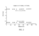
異なる温度で硬化させた接着剤の性能を、種々の温度及び湿度の条件下で試験した。プレポリマーを含む配合物Aを二つのアセンブリーに使用した。その内の一つを150℃で、もう一つを175℃で硬化した。それらのサンプルの落下試験結果が表7に示されている。
Example 5
The performance of the adhesive cured at different temperatures was tested under various temperature and humidity conditions. Formulation A containing the prepolymer was used in the two assemblies. One of them was cured at 150 ° C and the other at 175 ° C. The drop test results of these samples are shown in Table 7.
異なる温度での硬化と共に安定性を試験するために、接着剤をFR‐4板の上に設置して150℃で、セラミック基板上に設置して175℃で硬化した。両方のアセンブリーを湿気チャンバー中に配置させて、85℃/85%相対湿度で保管した。そのチャンバーから取り出した両方のサンプルの抵抗が図2に示されている。図2に示されるように、その接触抵抗は、過激な条件下で変化せず、硬化温度に依存していない。 To test the stability with curing at different temperatures, the adhesive was placed on a FR-4 plate at 150 ° C. and placed on a ceramic substrate and cured at 175 ° C. Both assemblies were placed in a humidity chamber and stored at 85 ° C./85% relative humidity. The resistance of both samples removed from the chamber is shown in FIG. As shown in FIG. 2, the contact resistance does not change under extreme conditions and does not depend on the curing temperature.
実施例6
実施例2中で説明した電気部品を含む試験体をFR‐r4板上に設置して、ダイシェアー(die shear)試験にかけた。ダイシェアー試験は、銅基板上での導電性接着剤の接着強度を実証するものである。Royce552dieなる自動ダイシェアー試験機を使用した。全ての実験を室温で実施した。基板上の部品は錫/鉛末端を有する0204零抵抗体である。ダイシェアー試験機から自動的に移動するチップ(tip)がその基板上の部品を押出し、最大の力がダイシェアー強度として記録される。それらの結果が表8に示されている。
Example 6
A test body including the electrical component described in Example 2 was placed on an FR-r4 plate and subjected to a die shear test. The die shear test demonstrates the bond strength of a conductive adhesive on a copper substrate. An automatic die shear tester, Royce 552die, was used. All experiments were performed at room temperature. The component on the substrate is a 0204 zero resistor with a tin / lead end. A tip that automatically moves from the die shear tester extrudes the part on the substrate, and the maximum force is recorded as the die shear strength. The results are shown in Table 8.
当業者に明らかであるように、本発明についての多くの修正及び変更が、その精神及び範囲から離れることなく成されることが可能である。ここに記載された特定の態様は、実施例のためのみに提供されるものであって、本発明は付与される請求項に均等な十分な範囲を伴う、請求項の語句によってのみ限定されるべきものである。 Many modifications and variations of this invention can be made without departing from its spirit and scope, as will be apparent to those skilled in the art. The specific embodiments described herein are provided by way of example only and the invention is limited only by the terms of the claims, with the full scope of equivalents to the claims being granted. It should be.
Claims (10)
(a)少なくとも1種のエポキシ樹脂と少なくとも1種の脂肪族ジアミンのプレポリマーを含む樹脂系であって、該エポキシ樹脂中のエポキシ官能基の該脂肪族ジアミン中のアミン官能基に対する比が1より大きい、樹脂系、
(b)導電性充填剤、
(c)腐蝕抑制剤、及び
(d)イミダゾールである、硬化剤、
を含む、熱硬化性組成物。A thermosetting composition for use in a microelectronic device, comprising:
(A) at least one epoxy resin and a prepolymer of at least one aliphatic di amine A including dendritic fat-based, amine in the aliphatic di amine Epoxy officer functional groups of the epoxy resin A resin system with a ratio to the functional group of greater than 1,
(B) a conductive filler,
(C) a corrosion inhibitor, and (d) a curing agent that is imidazole ,
The including thermosetting composition.
Applications Claiming Priority (2)
| Application Number | Priority Date | Filing Date | Title |
|---|---|---|---|
| US10/377,988 US7108806B2 (en) | 2003-02-28 | 2003-02-28 | Conductive materials with electrical stability and good impact resistance for use in electronics devices |
| PCT/US2004/004844 WO2004078870A1 (en) | 2003-02-28 | 2004-02-18 | Conductive adhesive compositions with electical stability and good impact resistance for use in electronics devices |
Publications (3)
| Publication Number | Publication Date |
|---|---|
| JP2006524286A JP2006524286A (en) | 2006-10-26 |
| JP2006524286A5 JP2006524286A5 (en) | 2010-07-15 |
| JP4602970B2 true JP4602970B2 (en) | 2010-12-22 |
Family
ID=32908192
Family Applications (1)
| Application Number | Title | Priority Date | Filing Date |
|---|---|---|---|
| JP2006508764A Expired - Fee Related JP4602970B2 (en) | 2003-02-28 | 2004-02-18 | Electrically stable and impact resistant conductive adhesive composition for electronic devices |
Country Status (8)
| Country | Link |
|---|---|
| US (1) | US7108806B2 (en) |
| EP (1) | EP1597332B1 (en) |
| JP (1) | JP4602970B2 (en) |
| KR (1) | KR101170395B1 (en) |
| CN (1) | CN100393836C (en) |
| AT (1) | ATE394459T1 (en) |
| DE (1) | DE602004013544D1 (en) |
| WO (1) | WO2004078870A1 (en) |
Families Citing this family (58)
| Publication number | Priority date | Publication date | Assignee | Title |
|---|---|---|---|---|
| AU2003270820A1 (en) * | 2003-03-18 | 2004-10-11 | Dow Corning Corporation | A conductive adhesive composition |
| US7527749B2 (en) * | 2004-10-18 | 2009-05-05 | Georgia Tech Research Corporation | Electrically conductive adhesives and methods of making |
| US7763188B2 (en) * | 2005-03-04 | 2010-07-27 | International Business Machines Corporation | Electrically stable copper filled electrically conductive adhesive |
| US20070049665A1 (en) * | 2005-08-25 | 2007-03-01 | Musa Osama M | Quinolinols and quinolinol derivatives as adhesion promoters in die attach adhesives |
| US7378523B2 (en) * | 2005-08-25 | 2008-05-27 | National Starch And Chemical Investment Holding Corporation | Quinolinols as fluxing and accelerating agents for underfill compositions |
| US7468407B2 (en) | 2005-09-26 | 2008-12-23 | National Starch And Chemical Investment Holding Copporation | Metal salts of quinolinols and quinolinol derivatives in curable compositions |
| JP5332102B2 (en) * | 2006-04-21 | 2013-11-06 | 日立化成株式会社 | Liquid composition, resistor, resistor element and wiring board |
| WO2008001740A1 (en) * | 2006-06-30 | 2008-01-03 | Asahi Kasei Emd Corporation | Conductive filler |
| GB0622060D0 (en) * | 2006-11-06 | 2006-12-13 | Hexcel Composites Ltd | Improved composite materials |
| US8069817B2 (en) * | 2007-03-30 | 2011-12-06 | Lam Research Corporation | Showerhead electrodes and showerhead electrode assemblies having low-particle performance for semiconductor material processing apparatuses |
| US8221552B2 (en) * | 2007-03-30 | 2012-07-17 | Lam Research Corporation | Cleaning of bonded silicon electrodes |
| CN101679603A (en) * | 2007-05-09 | 2010-03-24 | 陶氏环球技术公司 | Epoxy thermoset compositions comprising excess epoxy resin and process for the preparation thereof |
| PL2191482T3 (en) | 2007-09-13 | 2017-08-31 | Henkel Ag & Co. Kgaa | Electrically conductive composition |
| US8003016B2 (en) | 2007-09-28 | 2011-08-23 | Sabic Innovative Plastics Ip B.V. | Thermoplastic composition with improved positive temperature coefficient behavior and method for making thereof |
| KR100918345B1 (en) * | 2007-11-23 | 2009-09-22 | 제일모직주식회사 | Anisotropic conductive film composition?and film ?thereof |
| WO2009069111A2 (en) * | 2007-11-26 | 2009-06-04 | Dublin Institute Of Technology | Sol-gel coating compositions and their process of preparation |
| JP5921808B2 (en) * | 2008-04-30 | 2016-05-24 | 日立化成株式会社 | Connection material and semiconductor device |
| CN102650060B (en) * | 2009-06-26 | 2015-04-15 | 中国石油化工股份有限公司 | Composite corrosion inhibitor for butyl rubber chloromethane glycol dehydration and regeneration system |
| CN102650057B (en) * | 2009-06-26 | 2015-04-15 | 中国石油化工股份有限公司 | Composite corrosion inhibitor for butyl rubber chloromethane glycol dehydration and regeneration system |
| KR101637006B1 (en) * | 2009-08-19 | 2016-07-08 | 도레이첨단소재 주식회사 | Adhesive tape composition for electronic components |
| EP2493998A4 (en) * | 2009-10-27 | 2018-01-10 | Henkel IP & Holding GmbH | Thermal interface material with epoxidized nutshell oil |
| WO2011059942A2 (en) * | 2009-11-13 | 2011-05-19 | Henkel Corporation | Thermal interface material with phenyl ester |
| CN101781541B (en) * | 2010-02-02 | 2012-12-05 | 华南理工大学 | In situ preparation method of nano silver/epoxy conductive adhesive |
| GB201005444D0 (en) | 2010-03-31 | 2010-05-19 | 3M Innovative Properties Co | Epoxy adhesive compositions comprising an adhesion promoter |
| CN103119116B (en) * | 2010-05-26 | 2015-04-29 | 磁力技术涡轮声波公司 | Conductive adhesive |
| US9005485B2 (en) | 2011-03-22 | 2015-04-14 | Nano And Advanced Materials Institute Limited | High performance die attach adhesives (DAAs) nanomaterials for high brightness LED |
| WO2012129656A1 (en) | 2011-03-28 | 2012-10-04 | Turbosonic Inc. | Erosion-resistant conductive composite material collecting electrode for wesp |
| BR112013031427A2 (en) * | 2011-06-30 | 2017-04-25 | Dow Global Technologies Llc | curable epoxy resin system and process for forming a fiber reinforced epoxy composite |
| CN102304338A (en) * | 2011-07-08 | 2012-01-04 | 上海邦中高分子材料有限公司 | Bonding resin with conductive property |
| MY173371A (en) * | 2011-07-21 | 2020-01-21 | Hitachi Chemical Co Ltd | Conductive material |
| JP5802081B2 (en) * | 2011-08-24 | 2015-10-28 | 株式会社タムラ製作所 | Anisotropic conductive paste |
| US11027289B2 (en) | 2011-12-09 | 2021-06-08 | Durr Systems Inc. | Wet electrostatic precipitator system components |
| JP6169820B2 (en) * | 2012-03-30 | 2017-07-26 | 田中貴金属工業株式会社 | Conductive adhesive and method for producing the same |
| KR101525652B1 (en) | 2012-05-04 | 2015-06-03 | 삼성전기주식회사 | Conductive resin composition, multi layer ceramic capacitor having the same and manufacturing method thereof |
| US9200184B2 (en) | 2012-05-17 | 2015-12-01 | Henkel IP & Holding GmbH | Chain extended epoxy to improve adhesion of conductive die attach film |
| JP5970975B2 (en) * | 2012-06-26 | 2016-08-17 | 日立化成株式会社 | Epoxy resin molding material for sealing and electronic component device |
| TW201408754A (en) * | 2012-08-29 | 2014-03-01 | Compal Electronics Inc | Adhesive material and fabricating method of substrate structure having heat-shielding ability |
| CN102924906B (en) * | 2012-10-26 | 2017-10-03 | 深圳大学 | Composite of piezoresistive characteristic and preparation method thereof |
| WO2014196444A1 (en) * | 2013-06-03 | 2014-12-11 | 昭和電工株式会社 | Conductive resin composition for microwave heating |
| FR3006493A1 (en) * | 2013-06-04 | 2014-12-05 | Nexans | ELECTRICAL CABLE WITH MEDIUM OR HIGH VOLTAGE |
| WO2015001061A1 (en) * | 2013-07-03 | 2015-01-08 | Rhodia Operations | Curable composition and process for the manufacture of an epoxy thermoset |
| CN103409083B (en) * | 2013-08-22 | 2015-11-25 | 胡钧峰 | Graphite carbon black conductive adhesive and preparation method thereof |
| CN106164125B (en) * | 2014-02-24 | 2020-08-07 | Sika技术股份公司 | Furan-based amines as curing agents for epoxy resins in low VOC applications |
| WO2015129377A1 (en) * | 2014-02-25 | 2015-09-03 | ナミックス株式会社 | Electroconductive adhesive and semiconductor device |
| CN104927698A (en) * | 2014-03-17 | 2015-09-23 | 北京中科纳通电子技术有限公司 | Low-temperature conductive adhesive capable of being used for high-precision circuits |
| CN105111988B (en) * | 2015-10-09 | 2017-12-26 | 重庆文理学院 | A kind of compliant conductive elargol |
| JP5989928B1 (en) | 2016-02-10 | 2016-09-07 | 古河電気工業株式会社 | Conductive adhesive film and dicing die bonding film using the same |
| JP5972490B1 (en) | 2016-02-10 | 2016-08-17 | 古河電気工業株式会社 | Conductive adhesive composition, and conductive adhesive film and dicing / die bonding film using the same |
| JP6005312B1 (en) | 2016-02-10 | 2016-10-12 | 古河電気工業株式会社 | Conductive adhesive film and dicing die bonding film using the same |
| JP5972489B1 (en) | 2016-02-10 | 2016-08-17 | 古河電気工業株式会社 | Conductive adhesive film and dicing die bonding film using the same |
| JP6005313B1 (en) * | 2016-02-10 | 2016-10-12 | 古河電気工業株式会社 | Conductive adhesive film and dicing die bonding film using the same |
| KR102652817B1 (en) * | 2016-12-30 | 2024-04-01 | 엘지디스플레이 주식회사 | Adhesive film and foldable display device using the same |
| CN112391135B (en) * | 2019-08-14 | 2023-10-13 | 广州得尔塔影像技术有限公司 | Adhesive composition, and preparation method and application thereof |
| TW202219214A (en) | 2020-08-27 | 2022-05-16 | 德商漢高股份有限及兩合公司 | Electrically conductive one component (1k) epoxy formulation |
| CN112164685B (en) * | 2020-08-31 | 2023-03-31 | 浙江大学 | Organic-coated corrosion-resistant bonded silver wire and preparation method thereof |
| CN114231227A (en) * | 2020-09-09 | 2022-03-25 | 深圳斯巴达光电有限公司 | Epoxy resin composition and production method thereof |
| CN115044276B (en) * | 2022-07-22 | 2023-05-19 | 山东佰盛能源科技有限公司 | Pipeline anti-corrosion coating and production process thereof |
| CN115584231B (en) * | 2022-09-29 | 2023-11-03 | 哈尔滨工业大学(深圳) | Modified isotropic conductive adhesive for packaging and preparation method thereof |
Family Cites Families (13)
| Publication number | Priority date | Publication date | Assignee | Title |
|---|---|---|---|---|
| DE3901279A1 (en) * | 1989-01-18 | 1990-07-19 | Hoechst Ag | USE OF POLYAMIDOAMINES AS HARDENERS FOR EPOXY RESINS AND CONTAINABLE MIXTURES CONTAINING THEM |
| US5183593A (en) * | 1989-11-14 | 1993-02-02 | Poly-Flex Circuits, Inc. | Electrically conductive cement |
| DE4342722A1 (en) * | 1993-12-15 | 1995-06-22 | Hoechst Ag | Elastic epoxy resin hardener system |
| DE4342721A1 (en) * | 1993-12-15 | 1995-06-22 | Hoechst Ag | Elastic epoxy resin hardener system |
| US5717054A (en) * | 1995-06-07 | 1998-02-10 | National Starch & Chemical Investment Holding Corp. | Epoxy resins consisting of flexible chains terminated with glycidyloxyphenyl groups for use in microelectronics adhesives |
| JP2915379B2 (en) | 1996-06-18 | 1999-07-05 | レイセオン・カンパニー | Conductive adhesive resistant to drop impact |
| US6114413A (en) | 1997-07-10 | 2000-09-05 | International Business Machines Corporation | Thermally conducting materials and applications for microelectronic packaging |
| US5891367A (en) | 1998-02-23 | 1999-04-06 | General Motors Corporation | Conductive epoxy adhesive |
| US6344157B1 (en) | 1999-02-12 | 2002-02-05 | National Starch And Chemical Investment Holding Corporation | Conductive and resistive materials with electrical stability for use in electronics devices |
| JP2000273317A (en) * | 1999-02-12 | 2000-10-03 | Natl Starch & Chem Investment Holding Corp | Conductive and resisting material having electrical stability and used for electronic device |
| US6322848B1 (en) * | 1999-10-26 | 2001-11-27 | Lord Corporation | Flexible epoxy encapsulating material |
| US6583201B2 (en) | 2001-04-25 | 2003-06-24 | National Starch And Chemical Investment Holding Corporation | Conductive materials with electrical stability for use in electronics devices |
| US20030192643A1 (en) | 2002-03-15 | 2003-10-16 | Rainer Schoenfeld | Epoxy adhesive having improved impact resistance |
-
2003
- 2003-02-28 US US10/377,988 patent/US7108806B2/en not_active Expired - Fee Related
-
2004
- 2004-02-18 JP JP2006508764A patent/JP4602970B2/en not_active Expired - Fee Related
- 2004-02-18 WO PCT/US2004/004844 patent/WO2004078870A1/en active Application Filing
- 2004-02-18 CN CNB2004800052335A patent/CN100393836C/en not_active Expired - Fee Related
- 2004-02-18 KR KR1020057016031A patent/KR101170395B1/en not_active IP Right Cessation
- 2004-02-18 AT AT04712396T patent/ATE394459T1/en not_active IP Right Cessation
- 2004-02-18 EP EP04712396A patent/EP1597332B1/en not_active Expired - Lifetime
- 2004-02-18 DE DE602004013544T patent/DE602004013544D1/en not_active Expired - Fee Related
Also Published As
| Publication number | Publication date |
|---|---|
| EP1597332A1 (en) | 2005-11-23 |
| CN100393836C (en) | 2008-06-11 |
| EP1597332B1 (en) | 2008-05-07 |
| KR101170395B1 (en) | 2012-08-01 |
| CN1788062A (en) | 2006-06-14 |
| DE602004013544D1 (en) | 2008-06-19 |
| US20040169162A1 (en) | 2004-09-02 |
| WO2004078870A1 (en) | 2004-09-16 |
| KR20050105502A (en) | 2005-11-04 |
| ATE394459T1 (en) | 2008-05-15 |
| US7108806B2 (en) | 2006-09-19 |
| JP2006524286A (en) | 2006-10-26 |
Similar Documents
| Publication | Publication Date | Title |
|---|---|---|
| JP4602970B2 (en) | Electrically stable and impact resistant conductive adhesive composition for electronic devices | |
| TWI382076B (en) | Low stress conductive adhesive | |
| JP6967726B2 (en) | Solder paste and mounting structure | |
| US20110140162A1 (en) | Conductive adhesive and led substrate using the same | |
| US10294324B2 (en) | Resin composition, conductive resin composition, adhesive, conductive adhesive, paste for forming electrodes, and semiconductor device | |
| KR20020066988A (en) | Conductive and resistive materials with electrical stability for use in electronics devices | |
| US20080261049A1 (en) | Electroconductive Paste and Substrate Using the Same for Mounting Electronic Parts | |
| JP2004535480A (en) | Electrically stable conductive materials for use in electronic devices | |
| JP5225853B2 (en) | Resin paste for die bonding, semiconductor device manufacturing method, and semiconductor device | |
| JP2009019171A (en) | Die bonding paste | |
| JP5258191B2 (en) | Adhesive for semiconductor chip bonding | |
| JPWO2010070947A1 (en) | Resin paste for die bonding, semiconductor device manufacturing method, and semiconductor device | |
| JPH11284114A (en) | Semiconductor device | |
| JP2002201448A (en) | Electroconductive adhesive | |
| JP2016117869A (en) | Resin composition for semiconductor adhesion and semiconductor device | |
| JP2008075054A (en) | One-pack type epoxy resin composition | |
| JP3695226B2 (en) | One-part thermosetting resin composition | |
| JP2005317491A (en) | Conductive paste and electronic component mounting substrate using it | |
| JP2004352785A (en) | Anisotropic electroconductive adhesive | |
| JP2008112972A (en) | Resin paste for die bonding, method for manufacturing semiconductor device, and semiconductor device | |
| JP2010050017A (en) | Light-resistant conductive paste and element connecting method | |
| JP2003263921A (en) | Conductive paste | |
| JP2004043608A (en) | Electroconductive adhesive | |
| JP2006160913A (en) | Epoxy-based curable composition and electronic part | |
| JP2005317490A (en) | Conductive paste and electronic component mounting substrate using it |
Legal Events
| Date | Code | Title | Description |
|---|---|---|---|
| A521 | Request for written amendment filed |
Free format text: JAPANESE INTERMEDIATE CODE: A523 Effective date: 20070208 |
|
| A621 | Written request for application examination |
Free format text: JAPANESE INTERMEDIATE CODE: A621 Effective date: 20070208 |
|
| A977 | Report on retrieval |
Free format text: JAPANESE INTERMEDIATE CODE: A971007 Effective date: 20090805 |
|
| A131 | Notification of reasons for refusal |
Free format text: JAPANESE INTERMEDIATE CODE: A131 Effective date: 20100302 |
|
| A521 | Request for written amendment filed |
Free format text: JAPANESE INTERMEDIATE CODE: A523 Effective date: 20100531 |
|
| A524 | Written submission of copy of amendment under article 19 pct |
Free format text: JAPANESE INTERMEDIATE CODE: A524 Effective date: 20100531 |
|
| TRDD | Decision of grant or rejection written | ||
| A01 | Written decision to grant a patent or to grant a registration (utility model) |
Free format text: JAPANESE INTERMEDIATE CODE: A01 Effective date: 20100831 |
|
| A01 | Written decision to grant a patent or to grant a registration (utility model) |
Free format text: JAPANESE INTERMEDIATE CODE: A01 |
|
| A61 | First payment of annual fees (during grant procedure) |
Free format text: JAPANESE INTERMEDIATE CODE: A61 Effective date: 20100930 |
|
| FPAY | Renewal fee payment (event date is renewal date of database) |
Free format text: PAYMENT UNTIL: 20131008 Year of fee payment: 3 |
|
| R150 | Certificate of patent or registration of utility model |
Free format text: JAPANESE INTERMEDIATE CODE: R150 |
|
| FPAY | Renewal fee payment (event date is renewal date of database) |
Free format text: PAYMENT UNTIL: 20131008 Year of fee payment: 3 |
|
| FPAY | Renewal fee payment (event date is renewal date of database) |
Free format text: PAYMENT UNTIL: 20131008 Year of fee payment: 3 |
|
| S111 | Request for change of ownership or part of ownership |
Free format text: JAPANESE INTERMEDIATE CODE: R313113 Free format text: JAPANESE INTERMEDIATE CODE: R313111 |
|
| FPAY | Renewal fee payment (event date is renewal date of database) |
Free format text: PAYMENT UNTIL: 20131008 Year of fee payment: 3 |
|
| R350 | Written notification of registration of transfer |
Free format text: JAPANESE INTERMEDIATE CODE: R350 |
|
| R250 | Receipt of annual fees |
Free format text: JAPANESE INTERMEDIATE CODE: R250 |
|
| LAPS | Cancellation because of no payment of annual fees |