JP4592193B2 - Manufacturing method of semiconductor device - Google Patents
Manufacturing method of semiconductor device Download PDFInfo
- Publication number
- JP4592193B2 JP4592193B2 JP2001029779A JP2001029779A JP4592193B2 JP 4592193 B2 JP4592193 B2 JP 4592193B2 JP 2001029779 A JP2001029779 A JP 2001029779A JP 2001029779 A JP2001029779 A JP 2001029779A JP 4592193 B2 JP4592193 B2 JP 4592193B2
- Authority
- JP
- Japan
- Prior art keywords
- active region
- mos transistor
- film
- bird
- semiconductor device
- Prior art date
- Legal status (The legal status is an assumption and is not a legal conclusion. Google has not performed a legal analysis and makes no representation as to the accuracy of the status listed.)
- Expired - Fee Related
Links
- 239000004065 semiconductor Substances 0.000 title claims description 67
- 238000004519 manufacturing process Methods 0.000 title claims description 41
- 241000293849 Cordylanthus Species 0.000 claims description 51
- 238000002955 isolation Methods 0.000 claims description 32
- 238000000034 method Methods 0.000 claims description 22
- 239000000758 substrate Substances 0.000 claims description 22
- 239000012535 impurity Substances 0.000 claims description 9
- 230000002093 peripheral effect Effects 0.000 claims description 5
- 229910044991 metal oxide Inorganic materials 0.000 claims description 2
- 150000004706 metal oxides Chemical class 0.000 claims description 2
- 230000001590 oxidative effect Effects 0.000 claims 1
- 150000004767 nitrides Chemical class 0.000 description 21
- 238000012986 modification Methods 0.000 description 12
- 230000004048 modification Effects 0.000 description 12
- 230000015572 biosynthetic process Effects 0.000 description 8
- 230000003647 oxidation Effects 0.000 description 8
- 238000007254 oxidation reaction Methods 0.000 description 8
- 238000005229 chemical vapour deposition Methods 0.000 description 7
- 238000005468 ion implantation Methods 0.000 description 7
- 238000000926 separation method Methods 0.000 description 7
- 238000001039 wet etching Methods 0.000 description 5
- XUIMIQQOPSSXEZ-UHFFFAOYSA-N Silicon Chemical compound [Si] XUIMIQQOPSSXEZ-UHFFFAOYSA-N 0.000 description 4
- 230000000694 effects Effects 0.000 description 4
- 229910052710 silicon Inorganic materials 0.000 description 4
- 239000010703 silicon Substances 0.000 description 4
- 238000002513 implantation Methods 0.000 description 3
- 238000009413 insulation Methods 0.000 description 3
- VYPSYNLAJGMNEJ-UHFFFAOYSA-N Silicium dioxide Chemical compound O=[Si]=O VYPSYNLAJGMNEJ-UHFFFAOYSA-N 0.000 description 2
- 238000005530 etching Methods 0.000 description 2
- 239000000463 material Substances 0.000 description 2
- 229910021420 polycrystalline silicon Inorganic materials 0.000 description 2
- 229920005591 polysilicon Polymers 0.000 description 2
- 229910052814 silicon oxide Inorganic materials 0.000 description 2
- 238000013459 approach Methods 0.000 description 1
- 238000010586 diagram Methods 0.000 description 1
- 238000005498 polishing Methods 0.000 description 1
- 230000003068 static effect Effects 0.000 description 1
- 239000000126 substance Substances 0.000 description 1
Images


Classifications
-
- H—ELECTRICITY
- H01—ELECTRIC ELEMENTS
- H01L—SEMICONDUCTOR DEVICES NOT COVERED BY CLASS H10
- H01L29/00—Semiconductor devices adapted for rectifying, amplifying, oscillating or switching, or capacitors or resistors with at least one potential-jump barrier or surface barrier, e.g. PN junction depletion layer or carrier concentration layer; Details of semiconductor bodies or of electrodes thereof ; Multistep manufacturing processes therefor
- H01L29/66—Types of semiconductor device ; Multistep manufacturing processes therefor
- H01L29/68—Types of semiconductor device ; Multistep manufacturing processes therefor controllable by only the electric current supplied, or only the electric potential applied, to an electrode which does not carry the current to be rectified, amplified or switched
- H01L29/76—Unipolar devices, e.g. field effect transistors
- H01L29/772—Field effect transistors
- H01L29/78—Field effect transistors with field effect produced by an insulated gate
-
- H—ELECTRICITY
- H01—ELECTRIC ELEMENTS
- H01L—SEMICONDUCTOR DEVICES NOT COVERED BY CLASS H10
- H01L21/00—Processes or apparatus adapted for the manufacture or treatment of semiconductor or solid state devices or of parts thereof
- H01L21/02—Manufacture or treatment of semiconductor devices or of parts thereof
- H01L21/04—Manufacture or treatment of semiconductor devices or of parts thereof the devices having at least one potential-jump barrier or surface barrier, e.g. PN junction, depletion layer or carrier concentration layer
- H01L21/18—Manufacture or treatment of semiconductor devices or of parts thereof the devices having at least one potential-jump barrier or surface barrier, e.g. PN junction, depletion layer or carrier concentration layer the devices having semiconductor bodies comprising elements of Group IV of the Periodic System or AIIIBV compounds with or without impurities, e.g. doping materials
- H01L21/28—Manufacture of electrodes on semiconductor bodies using processes or apparatus not provided for in groups H01L21/20 - H01L21/268
- H01L21/28008—Making conductor-insulator-semiconductor electrodes
- H01L21/28017—Making conductor-insulator-semiconductor electrodes the insulator being formed after the semiconductor body, the semiconductor being silicon
- H01L21/28158—Making the insulator
- H01L21/28167—Making the insulator on single crystalline silicon, e.g. using a liquid, i.e. chemical oxidation
- H01L21/28194—Making the insulator on single crystalline silicon, e.g. using a liquid, i.e. chemical oxidation by deposition, e.g. evaporation, ALD, CVD, sputtering, laser deposition
-
- H—ELECTRICITY
- H01—ELECTRIC ELEMENTS
- H01L—SEMICONDUCTOR DEVICES NOT COVERED BY CLASS H10
- H01L21/00—Processes or apparatus adapted for the manufacture or treatment of semiconductor or solid state devices or of parts thereof
- H01L21/70—Manufacture or treatment of devices consisting of a plurality of solid state components formed in or on a common substrate or of parts thereof; Manufacture of integrated circuit devices or of parts thereof
- H01L21/71—Manufacture of specific parts of devices defined in group H01L21/70
- H01L21/76—Making of isolation regions between components
- H01L21/762—Dielectric regions, e.g. EPIC dielectric isolation, LOCOS; Trench refilling techniques, SOI technology, use of channel stoppers
- H01L21/76202—Dielectric regions, e.g. EPIC dielectric isolation, LOCOS; Trench refilling techniques, SOI technology, use of channel stoppers using a local oxidation of silicon, e.g. LOCOS, SWAMI, SILO
- H01L21/76205—Dielectric regions, e.g. EPIC dielectric isolation, LOCOS; Trench refilling techniques, SOI technology, use of channel stoppers using a local oxidation of silicon, e.g. LOCOS, SWAMI, SILO in a region being recessed from the surface, e.g. in a recess, groove, tub or trench region
-
- H—ELECTRICITY
- H01—ELECTRIC ELEMENTS
- H01L—SEMICONDUCTOR DEVICES NOT COVERED BY CLASS H10
- H01L21/00—Processes or apparatus adapted for the manufacture or treatment of semiconductor or solid state devices or of parts thereof
- H01L21/70—Manufacture or treatment of devices consisting of a plurality of solid state components formed in or on a common substrate or of parts thereof; Manufacture of integrated circuit devices or of parts thereof
- H01L21/77—Manufacture or treatment of devices consisting of a plurality of solid state components or integrated circuits formed in, or on, a common substrate
- H01L21/78—Manufacture or treatment of devices consisting of a plurality of solid state components or integrated circuits formed in, or on, a common substrate with subsequent division of the substrate into plural individual devices
- H01L21/82—Manufacture or treatment of devices consisting of a plurality of solid state components or integrated circuits formed in, or on, a common substrate with subsequent division of the substrate into plural individual devices to produce devices, e.g. integrated circuits, each consisting of a plurality of components
- H01L21/822—Manufacture or treatment of devices consisting of a plurality of solid state components or integrated circuits formed in, or on, a common substrate with subsequent division of the substrate into plural individual devices to produce devices, e.g. integrated circuits, each consisting of a plurality of components the substrate being a semiconductor, using silicon technology
- H01L21/8232—Field-effect technology
- H01L21/8234—MIS technology, i.e. integration processes of field effect transistors of the conductor-insulator-semiconductor type
- H01L21/823437—MIS technology, i.e. integration processes of field effect transistors of the conductor-insulator-semiconductor type with a particular manufacturing method of the gate conductors, e.g. particular materials, shapes
- H01L21/823456—MIS technology, i.e. integration processes of field effect transistors of the conductor-insulator-semiconductor type with a particular manufacturing method of the gate conductors, e.g. particular materials, shapes gate conductors with different shapes, lengths or dimensions
-
- H—ELECTRICITY
- H01—ELECTRIC ELEMENTS
- H01L—SEMICONDUCTOR DEVICES NOT COVERED BY CLASS H10
- H01L21/00—Processes or apparatus adapted for the manufacture or treatment of semiconductor or solid state devices or of parts thereof
- H01L21/70—Manufacture or treatment of devices consisting of a plurality of solid state components formed in or on a common substrate or of parts thereof; Manufacture of integrated circuit devices or of parts thereof
- H01L21/77—Manufacture or treatment of devices consisting of a plurality of solid state components or integrated circuits formed in, or on, a common substrate
- H01L21/78—Manufacture or treatment of devices consisting of a plurality of solid state components or integrated circuits formed in, or on, a common substrate with subsequent division of the substrate into plural individual devices
- H01L21/82—Manufacture or treatment of devices consisting of a plurality of solid state components or integrated circuits formed in, or on, a common substrate with subsequent division of the substrate into plural individual devices to produce devices, e.g. integrated circuits, each consisting of a plurality of components
- H01L21/822—Manufacture or treatment of devices consisting of a plurality of solid state components or integrated circuits formed in, or on, a common substrate with subsequent division of the substrate into plural individual devices to produce devices, e.g. integrated circuits, each consisting of a plurality of components the substrate being a semiconductor, using silicon technology
- H01L21/8232—Field-effect technology
- H01L21/8234—MIS technology, i.e. integration processes of field effect transistors of the conductor-insulator-semiconductor type
- H01L21/823462—MIS technology, i.e. integration processes of field effect transistors of the conductor-insulator-semiconductor type with a particular manufacturing method of the gate insulating layers, e.g. different gate insulating layer thicknesses, particular gate insulator materials or particular gate insulator implants
-
- H—ELECTRICITY
- H01—ELECTRIC ELEMENTS
- H01L—SEMICONDUCTOR DEVICES NOT COVERED BY CLASS H10
- H01L21/00—Processes or apparatus adapted for the manufacture or treatment of semiconductor or solid state devices or of parts thereof
- H01L21/70—Manufacture or treatment of devices consisting of a plurality of solid state components formed in or on a common substrate or of parts thereof; Manufacture of integrated circuit devices or of parts thereof
- H01L21/77—Manufacture or treatment of devices consisting of a plurality of solid state components or integrated circuits formed in, or on, a common substrate
- H01L21/78—Manufacture or treatment of devices consisting of a plurality of solid state components or integrated circuits formed in, or on, a common substrate with subsequent division of the substrate into plural individual devices
- H01L21/82—Manufacture or treatment of devices consisting of a plurality of solid state components or integrated circuits formed in, or on, a common substrate with subsequent division of the substrate into plural individual devices to produce devices, e.g. integrated circuits, each consisting of a plurality of components
- H01L21/822—Manufacture or treatment of devices consisting of a plurality of solid state components or integrated circuits formed in, or on, a common substrate with subsequent division of the substrate into plural individual devices to produce devices, e.g. integrated circuits, each consisting of a plurality of components the substrate being a semiconductor, using silicon technology
- H01L21/8232—Field-effect technology
- H01L21/8234—MIS technology, i.e. integration processes of field effect transistors of the conductor-insulator-semiconductor type
- H01L21/823481—MIS technology, i.e. integration processes of field effect transistors of the conductor-insulator-semiconductor type isolation region manufacturing related aspects, e.g. to avoid interaction of isolation region with adjacent structure
-
- H—ELECTRICITY
- H01—ELECTRIC ELEMENTS
- H01L—SEMICONDUCTOR DEVICES NOT COVERED BY CLASS H10
- H01L29/00—Semiconductor devices adapted for rectifying, amplifying, oscillating or switching, or capacitors or resistors with at least one potential-jump barrier or surface barrier, e.g. PN junction depletion layer or carrier concentration layer; Details of semiconductor bodies or of electrodes thereof ; Multistep manufacturing processes therefor
- H01L29/02—Semiconductor bodies ; Multistep manufacturing processes therefor
- H01L29/06—Semiconductor bodies ; Multistep manufacturing processes therefor characterised by their shape; characterised by the shapes, relative sizes, or dispositions of the semiconductor regions ; characterised by the concentration or distribution of impurities within semiconductor regions
-
- H—ELECTRICITY
- H01—ELECTRIC ELEMENTS
- H01L—SEMICONDUCTOR DEVICES NOT COVERED BY CLASS H10
- H01L29/00—Semiconductor devices adapted for rectifying, amplifying, oscillating or switching, or capacitors or resistors with at least one potential-jump barrier or surface barrier, e.g. PN junction depletion layer or carrier concentration layer; Details of semiconductor bodies or of electrodes thereof ; Multistep manufacturing processes therefor
- H01L29/40—Electrodes ; Multistep manufacturing processes therefor
- H01L29/41—Electrodes ; Multistep manufacturing processes therefor characterised by their shape, relative sizes or dispositions
- H01L29/423—Electrodes ; Multistep manufacturing processes therefor characterised by their shape, relative sizes or dispositions not carrying the current to be rectified, amplified or switched
- H01L29/42312—Gate electrodes for field effect devices
- H01L29/42316—Gate electrodes for field effect devices for field-effect transistors
- H01L29/4232—Gate electrodes for field effect devices for field-effect transistors with insulated gate
- H01L29/42364—Gate electrodes for field effect devices for field-effect transistors with insulated gate characterised by the insulating layer, e.g. thickness or uniformity
- H01L29/42368—Gate electrodes for field effect devices for field-effect transistors with insulated gate characterised by the insulating layer, e.g. thickness or uniformity the thickness being non-uniform
-
- H—ELECTRICITY
- H10—SEMICONDUCTOR DEVICES; ELECTRIC SOLID-STATE DEVICES NOT OTHERWISE PROVIDED FOR
- H10B—ELECTRONIC MEMORY DEVICES
- H10B10/00—Static random access memory [SRAM] devices
-
- Y—GENERAL TAGGING OF NEW TECHNOLOGICAL DEVELOPMENTS; GENERAL TAGGING OF CROSS-SECTIONAL TECHNOLOGIES SPANNING OVER SEVERAL SECTIONS OF THE IPC; TECHNICAL SUBJECTS COVERED BY FORMER USPC CROSS-REFERENCE ART COLLECTIONS [XRACs] AND DIGESTS
- Y10—TECHNICAL SUBJECTS COVERED BY FORMER USPC
- Y10S—TECHNICAL SUBJECTS COVERED BY FORMER USPC CROSS-REFERENCE ART COLLECTIONS [XRACs] AND DIGESTS
- Y10S257/00—Active solid-state devices, e.g. transistors, solid-state diodes
- Y10S257/903—FET configuration adapted for use as static memory cell
- Y10S257/904—FET configuration adapted for use as static memory cell with passive components,, e.g. polysilicon resistors
Landscapes
- Engineering & Computer Science (AREA)
- Power Engineering (AREA)
- Microelectronics & Electronic Packaging (AREA)
- General Physics & Mathematics (AREA)
- Computer Hardware Design (AREA)
- Physics & Mathematics (AREA)
- Condensed Matter Physics & Semiconductors (AREA)
- Manufacturing & Machinery (AREA)
- Ceramic Engineering (AREA)
- Chemical & Material Sciences (AREA)
- General Chemical & Material Sciences (AREA)
- Crystallography & Structural Chemistry (AREA)
- Chemical Kinetics & Catalysis (AREA)
- Element Separation (AREA)
- Insulated Gate Type Field-Effect Transistor (AREA)
- Semiconductor Memories (AREA)
- Metal-Oxide And Bipolar Metal-Oxide Semiconductor Integrated Circuits (AREA)
Description
【0001】
【発明の属する技術分野】
本発明は、半導体装置およびその製造方法に関し、より特定的には、活性領域表面が全体にわたってラウンド形状であるMOS(Metal Oxide Semiconductor)トランジスタを有する半導体装置およびその製造方法に関する。
【0002】
【従来の技術】
図21に、従来のMOSトランジスタの断面構造の一例を示す。この図に示すように、半導体基板1の主表面に選択的に分離酸化膜5を形成し、分離酸化膜5間に位置する活性領域11上に酸化膜8を介してゲート電極9を形成する。
【0003】
次に、図22および図23を用いて、図21に示すMOSトランジスタの製造方法について説明する。図22および図23は、上記MOSトランジスタの製造工程の特徴的な第1および第2工程を示す断面図である。
【0004】
まず半導体基板1の主表面上にマスク膜(図示せず)を形成し、このマスク膜を用いて酸化処理を行なうことにより図22に示すように分離酸化膜5を形成する。次に、図22に示すように、イオン注入時のダメージ防止用の酸化膜7を形成し、MOSトランジスタ形成のためのイオン注入を行なう。
【0005】
その後、図23に示すように、イオン注入時に用いた酸化膜7をHF等によるウェトエッチングで除去する。このとき、分離酸化膜5もエッチングされ、リセス部12が形成される。
【0006】
次に、図21に示すように、MOSトランジスタのゲート酸化膜となる酸化膜8とゲート電極9とを形成する。
【0007】
次に、図24〜図26を用いて、他の従来例について説明する。図24は、従来のSRAM(Static Random Access Memory)のメモリセルにおけるアクセスMOSトランジスタ部とドライバMOSトランジスタ部の断面構造図である。
【0008】
一般にSRAMのメモリセルでは、セル動作を安定させるためアクセスMOSトランジスタとドライバMOSトランジスタの電流比を大きくする必要がある。アクセスMOSトランジスタの電流値は小さい程良く、ドライバMOSトランジスタ電流値は大きい程良い。
【0009】
したがって、ドライバMOSトランジスタの活性領域11の幅Wdは、アクセスMOSトランジスタの活性領域11の幅Waよりも大きく、ドライバMOSトランジスタのゲート長Ldは、アクセスMOSトランジスタのゲート長Laより短くなっている。
【0010】
また、SRAMのメモリセルトランジスタに要求される特性として次のようなものもある。アクセスMOSトランジスタではバックバイアス時のしきい値電圧Vthが低い方が望ましく、またゲート長も長いことから、チャネルドープ注入は、バックバイアス効果が抑制される低エネルギーで行なうことが好ましい。
【0011】
他方、ドライバMOSトランジスタについては、ゲート長が短いことから、パンチスルーを抑制するため、チャネルドープ注入は高エネルギーで行なうことが好ましい。
【0012】
次に、図24に示すSRAMのメモリセルの製造方法について説明する。図25および図26は、図24に示すSRAMのメモリセルの製造工程の特徴的な第1および第2工程を示す断面図である。
【0013】
上述のMOSトランジスタの場合と同様に、半導体基板1上にマスク膜を形成し、このマスク膜を用いて酸化処理を行なう。それにより、図25に示すように分離酸化膜5を形成する。
【0014】
次に、図25に示すようにイオン注入時のダメージ防止のための酸化膜7を形成した後、アクセスMOSトランジスタおよびドライバMOSトランジスタ形成のためのイオン注入を行なう。
【0015】
このとき、酸化膜7の厚みは、アクセスMOSトランジスタ形成部とドライバMOSトランジスタ形成部とで同一である。
【0016】
次に、図26に示すように酸化膜7をHF等を用いたウェットエッチングで除去し、その後図24に示すようにアクセスMOSトランジスタおよびドライバMOSトランジスタのゲート酸化膜となる酸化膜8およびゲート電極9を形成する。
【0017】
【発明が解決しようとする課題】
上述のように図21に示すMOSトランジスタでは、分離酸化膜5のエッジにリセス部12が発生する。このリセス部12のため、MOSトランジスタでリーク電流が発生するという問題があった。この問題は、図24に示す例でも同様に生じ得る。
【0018】
また、上述のように図24に示すアクセスMOSトランジスタおよびドライバMOSトランジスタのチャネル注入を行なう時の酸化膜7の厚みは同一であるので、アクセスMOSトランジスタ形成領域とドライバMOSトランジスタ形成領域の一方を覆うマスク膜を形成する等の処理をしなければアクセスMOSトランジスタとドライバMOSトランジスタのチャネルドープ領域の深さを変えることはできなかった。
【0019】
さらに、別途絶縁膜を形成する工程を追加せずに、アクセスMOSトランジスタとドライバMOSトランジスタのゲート絶縁膜の厚みを変えることもできなかった。
【0020】
つまり、新たな工程を追加することなくSRAMにおけるメモリセルの性能を向上し、また動作を安定化することは困難であった。
【0021】
本発明は上記の課題を解決するためになされたものである。本発明の1つの目的は、MOSトランジスタを有する半導体装置のリーク電流を低減することにある。本発明の他の目的は、新たな工程を追加することなくSRAMにおけるメモリセルの性能を向上し、また動作を安定化することにある。
【0037】
【課題を解決するための手段】
本発明に係る半導体装置の製造方法は、アクセスMOSトランジスタとドライバMOSトランジスタとを備えたSRAMを有する半導体装置の製造方法であって、下記の各工程を備える。半導体基板の分離領域を露出し、アクセスMOSトランジスタが形成される第1活性領域と、ドライバMOSトランジスタが形成される第2活性領域とをそれぞれ覆うように半導体基板上に第1マスク膜と第2マスク膜を形成する。第1マスク膜と第2マスク膜を用いて半導体基板を選択的に酸化することにより、第1活性領域全体を覆いかつ第2活性領域の周縁部のみを覆うバーズビーク部を形成する。第1マスク膜と第2マスク膜を除去した後に第1活性領域上と第2活性領域上に第1絶縁膜と第2絶縁膜をそれぞれ形成する。第1絶縁膜およびバーズビーク部を通して第1活性領域に不純物を注入するとともに、第2絶縁膜を通して第2活性領域に不純物を注入して第1活性領域の浅い位置にチャネルドープを行ないながら、第2活性領域の深い位置にチャネルドープを行なう。第1絶縁膜と第2絶縁膜を除去した後に第1活性領域上および第2活性領域上にそれぞれ第3絶縁膜と第4絶縁膜を介して第1ゲート電極と第2ゲート電極をそれぞれ形成する。
【0038】
上記のようにバーズビーク部で第1活性領域全体を覆うことにより、第1と第2活性領域上に第1と第2絶縁膜を形成した際に、第1活性領域上に形成される絶縁膜の厚みを第2活性領域上に形成される絶縁膜の厚みよりも大きくすることができる。かかる下敷き絶縁膜を通してチャネルドープ注入を行なうので、チャネルドープ注入時の下敷き絶縁膜の厚みを第2活性領域上よりも第1活性領域上で大きくすることができ、第1活性領域におけるチャネルドープ深さを第2活性領域のそれよりも浅くすることができる。つまり、アクセスMOSトランジスタのチャネルドープ深さを、ドライバMOSトランジスタのチャネルドープ深さよりも浅くすることができる。このとき、第1活性領域上でバーズビーク部を繋ぐようにするだけで良いので、新たな工程を追加する必要はない。
【0039】
バーズビーク部の形成工程は、好ましくは、第1活性領域上でバーズビーク部を接続することにより第1活性領域表面が全体にわたってラウンド形状となるようにバーズビーク部を形成する工程を含む。
【0040】
それにより、アクセスMOSトランジスタの周囲の分離領域エッジにリセス部が生じるのを抑制することができる。
【0041】
第1と第2絶縁膜の除去工程は、第1活性領域上にバーズビーク部を残しながら第2活性領域の表面を露出させる工程を含む。
【0042】
それにより、アクセスMOSトランジスタのゲート絶縁膜の厚みを、ドライバMOSトランジスタのゲート絶縁膜の厚みよりも実質的に大きくすることができ、アクセスMOSトランジスタの電流値を減少させることができる。その結果、メモリセルの動作を安定化することができる。
【0043】
【発明の実施の形態】
以下、図1〜図20を用いて、本発明の実施の形態について説明する。
【0044】
(実施の形態1)
図1は、本発明の実施の形態1における半導体装置のMOSトランジスタ部の断面図である。図1に示すように、本実施の形態におけるMOSトランジスタは、半導体基板1の主表面に選択的に設けられた分離領域で囲まれる活性領域上に形成される。
【0045】
分離領域には、分離酸化膜5等の分離絶縁膜が形成される。分離酸化膜5は、たとえば後述するLOCOS(Local Oxidation of Silicon)法等で形成され、活性領域上に延びるバーズビーク部を有する。図1に示す例では、バーズビーク部は活性領域を覆っていないが、バーズビーク部で活性領域を覆うようにしてもよい。
【0046】
図1に示すように、分離酸化膜5のエッジには従来例のようなリセス部が存在せず、分離酸化膜5のエッジ近傍における酸化膜(絶縁膜)の厚みは大きくなっている。それにより、MOSトランジスタにおけるリーク電流を抑制することができる。
【0047】
また、分離酸化膜5間に位置する活性領域の表面は、全体にわたって上方に凸なラウンド形状を有し、分離領域に近づくにつれて下方に傾斜する。該活性領域の表面は、好ましくは、その中央部から周縁部に向かって所定の曲率を有する曲面で構成され、上記中央部から周縁部に向かうにつれて徐々に下方に傾斜する。活性領域の表面が上記の構造を有することも、分離領域エッジにおける酸化膜の厚みを大きくすることに寄与し得る。
【0048】
活性領域表面にチャネルドープ領域13を形成し、該活性領域上に酸化膜8を介してゲート電極9を形成し、ゲート電極9の両側にソース/ドレインとなる1組の不純物領域(図示せず)を形成する。
【0049】
次に、図2〜図7を用いて本実施の形態における半導体装置の製造方法について説明する。図2〜図7は、本実施の形態における半導体装置の製造工程の第1工程〜第6工程を示す断面図である。
【0050】
図2に示すように、半導体基板1の主表面上に、CVD(Chemical vapor deposition)法等を用いて、シリコン酸化膜、シリコン窒化酸化膜、ポリシリコン膜等からなるバッファ膜2を形成し、バッファ膜2上にCVD法等により窒化膜3を形成する。この窒化膜3上にレジストパターン4を形成する。
【0051】
次に、レジストパターン4を用いて窒化膜3とバッファ膜2とをエッチングする。それにより、図3に示すように、活性領域上に窒化膜3とバッファ膜2の積層膜(マスク膜)を残すことができる。このとき、半導体基板1の主表面はオーバーエッチングされ、若干の凹部が形成される。その後、レジストパターン4を除去する。
【0052】
次に、窒化膜3とバッファ膜2をマスクとして半導体基板1を選択的に熱酸化する。それにより、図4に示すように分離酸化膜5を形成する。
【0053】
このとき、バッファ膜2の材質、膜厚および窒化膜3の膜厚を調節することにより分離酸化膜5のバーズビーク部6の長さを調節することができ、活性領域上でバーズビーク部6を接続することができる。それにより、図4に示すように活性領域をバーズビーク部6で覆うことができる。
【0054】
たとえば、フィールド酸化をH2,O2ガス中で1050℃の条件で400nm以下程度行なう場合、バーズビーク部6の長さを0.25μmとすることができる。したがって、活性領域幅が0.5μm以下(活性領域幅がバーズビーク部6の長さの2倍以下)であれば、バーズビーク部6を活性領域上で繋ぐことができる。
【0055】
なお、上記のフィールド酸化におけるバッファ膜2の材質はシリコン窒化酸化膜(SION)であり、その膜厚は10nm程度であり、窒化膜3の膜厚は63nm程度である。
【0056】
図4に示すように分離領域近傍に位置する上記バーズビーク部6の厚みは、活性領域の中央部上に位置するバーズビーク部6の厚みよりも大きく、活性領域表面が全体にわたってラウンド形状となっている。それにより、分離領域のエッジにおける酸化膜(絶縁膜)の厚みを大きくすることができる。
【0057】
図5に示すように窒化膜3とバッファ膜2をエッチング等により除去した後、図6に示すようにバーズビーク部6上にイオン注入時のダメージ防止のための酸化膜7を形成する。その後、酸化膜7およびバーズビーク部6を通して所定の不純物を活性領域に注入し、MOSトランジスタ形成のためのチャネルドープを行なう。それにより、チャネルドープ領域13を形成する。
【0058】
次に、図7に示すようにHF等を用いたウェットエッチングにより酸化膜7を除去する。このとき、上記のように分離領域エッジにおける酸化膜の厚みが大きくなっているので、分離領域エッジに従来例のようなリセス部が生じるのを抑制することができる。
【0059】
その後、MOSトランジスタのゲート酸化膜となる酸化膜8およびゲート電極9をCVD法等により形成し、図1に示す構造が得られる。
【0060】
次に、本実施の形態1の変形例について図8〜図10を用いて説明する。図8は、本変形例におけるMOSトランジスタ部の断面図である。
【0061】
上記の実施の形態1ではLOCOSタイプの分離に本発明を適用した場合について説明したが、本発明の思想は、トレンチタイプの分離に対しても適用可能である。
【0062】
図8に示すように、本変形例では、半導体基板1の主表面にトレンチ10を形成し、トレンチ10内部に分離酸化膜5を形成している。それ以外の構成については実施の形態1の場合とほぼ同様であるので、重複説明は省略する。なお、図8に示す本変形例においてもバーズビーク部6は活性領域上で不連続となっているが、バーズビーク部6を活性領域上で接続しても良い。
【0063】
次に図9と図10を用いて、本変形例の製造方法について説明する。図9と図10は、本変形例の製造工程における特徴的な第1および第2工程を示す断面図である。
【0064】
まず、実施の形態1と同様の手法で半導体基板1の主表面上にバッファ膜2、窒化膜3およびレジストパターン4を形成し、レジストパターン4をマスクとしてバッファ膜2および窒化膜3をパターニングし、その後さらに半導体基板1をエッチングして図9に示すようにトレンチ10を形成する。
【0065】
次に、レジストパターン4を除去し、バッファ膜2および窒化膜3をマスクとして選択酸化を行ない、バーズビーク部6を活性領域上で繋ぐ。その後、酸化膜を堆積し、CMP(Chemical Mechanical Polishing)法等を用いて酸化膜を研磨する。それにより、図10に示すようにトレンチ10内に酸化膜を埋め込むことができる。
【0066】
それ以降は実施の形態1と同様の工程を経て図8に示す構造が得られる。
(実施の形態2)
次に、本発明の実施の形態2について図11〜図20を用いて説明する。図11は、本実施の形態2の半導体装置におけるアクセスMOSトランジスタ部とドライバMOSトランジスタ部を示す断面図である。
【0067】
本実施の形態2では、本発明をSRAMに適用している。該SRAMは、図11に示すようにアクセスMOSトランジスタとドライバMOSトランジスタとを含む。そして、アクセスMOSトランジスタ形成部の活性領域(以下「第1活性領域」と称する)表面を、実施の形態1の場合と同様に、全体にわたって上方に凸なラウンド形状とする。
【0068】
それにより、分離領域エッジにおける酸化膜の厚みを大きくすることができ、実施の形態1の場合と同様に分離領域エッジにおけるリセス部の発生を抑制することができる。それにより、アクセスMOSトランジスタにおけるリーク電流を抑制することができる。
【0069】
また、アクセスMOSトランジスタのチャネルドープ領域13aの深さD1を、ドライバMOSトランジスタのチャネルドープ領域13bの深さD2よりも浅くする。
【0070】
それにより、アクセスMOSトランジスタのバックバイアス効果を抑制しながらドライバMOSトランジスタにおけるパンチスルーを抑制することができ、メモリセルの性能を向上することができる。
【0071】
また、アクセスMOSトランジスタのゲート絶縁膜(酸化膜8とバーズビーク部6の積層膜)の厚みt1を、ドライバMOSトランジスタのゲート絶縁膜(酸化膜8)の厚みt2よりも大きくする。それにより、アクセスMOSトランジスタの電流量を減少させることができ、メモリセルの動作の安定化を図ることができる。
【0072】
また、第1活性領域の幅W1を、ドライバMOSトランジスタ形成部の活性領域(以下「第2活性領域」と称する)の幅W2よりも小さくする。
【0073】
それにより、アクセスMOSトランジスタとドライバMOSトランジスタの電流比を大きくしてメモリセル動作を安定化するとともに、第1活性領域上ではバーズビーク部6を接続しながら第2活性領域上でバーズビーク部6を分離することができる。
【0074】
次に、本実施の形態2における半導体装置の製造方法について図12〜図17を用いて、説明する。図12〜図17は、本実施の形態2における半導体装置の製造工程の第1工程〜第6工程を示す断面図である。
【0075】
図12に示すように、半導体基板1の主表面上に、CVD法等を用いて、シリコン酸化膜、シリコン窒化酸化膜、ポリシリコン膜等からなるバッファ膜2を形成し、バッファ膜2上にCVD法等により窒化膜3を形成する。第1および第2活性領域上に位置する窒化膜3上にレジストパターン4を形成する。
【0076】
次に、レジストパターン4を用いて窒化膜3とバッファ膜2をエッチングする。それにより、図13に示すように、第1および第2活性領域上に窒化膜3とバッファ膜2の積層膜(第1および第2マスク膜)を残すことができる。このとき、半導体基板1の主表面はオーバーエッチングされ、若干の凹部が形成される。その後、レジストパターン4を除去する。
【0077】
次に、窒化膜3とバッファ膜2をマスクとして半導体基板1を選択的に熱酸化する。それにより、図14に示すように第1および第2活性領域の周囲に分離酸化膜5を形成する。
【0078】
ここで、上述のように第1活性領域幅W1を第2活性領域幅W2よりも小さくすることにより、第1活性領域上でバーズビーク部6を繋ぎ、第2活性領域上でバーズビーク部6を分離することができる。つまり、第1活性領域全体をバーズビーク部6で覆いながら、第2活性領域の周縁部のみをバーズビーク部で覆うことができる。
【0079】
たとえば、実施の形態1の場合と同様の条件でフィールド酸化を400nm以下程度行なう場合、第1活性領域幅W1を0.5μm以下とし、第2活性領域幅W2を0.7μm以上程度とする。それにより、バーズビーク部6を第1活性領域上で繋ぎながら、第2活性領域上で分離することができる。
【0080】
上記のように第1活性領域全体をバーズビーク部6で覆うことにより、図14に示すように第1活性領域の表面が全体にわたってラウンド形状となる。
【0081】
次に、図15に示すように窒化膜3とバッファ膜2をエッチング等により除去する。このとき、第1活性領域はバーズビーク部6で覆われているが、第2活性領域は露出する。
【0082】
次に、図16に示すように、バーズビーク部6上と第2活性領域上とに、イオン注入時のダメージ防止のための酸化膜7を形成する。その後、所定の不純物を各活性領域に注入し、アクセスMOSトランジスタおよびドライバMOSトランジスタ形成のためのチャネルドープを行なう。
【0083】
このとき、第1活性領域には、酸化膜7およびバーズビーク部6を通して不純物を注入し、第2活性領域には、酸化膜7を通して不純物を注入する。酸化膜7およびバーズビーク部6の合計の厚みt3は、たとえば30nm程度であり、第2活性領域上の酸化膜7の厚みt4(たとえば15nm程度)よりも大きいので、第1活性領域の浅い位置にチャネルドープを行ないながら、第2活性領域の深い位置にチャネルドープを行なうことができる。
【0084】
それにより、アクセスMOSトランジスタのチャネルドープ領域13aの深さD1(たとえば130nm程度)を、ドライバMOSトランジスタのチャネルドープ領域13bの深さD2(たとえば145nm程度)よりも浅くすることができる。
【0085】
また、第1活性領域上にバーズビーク部6を残すだけでよいので、新たな工程は不要である。
【0086】
次に、図17に示すようにHF等を用いたウェットエッチングにより酸化膜7を除去する。このとき、アクセスMOSトランジスタ形成部では酸化膜7下に厚いバーズビーク部6が存在するので、上記ウェットエッチング後に第1活性領域上にバーズビーク部6を残しながら第2活性領域上の酸化膜7を除去することができる。
【0087】
また、アクセスMOSトランジスタの分離領域エッジにおける分離酸化膜5の厚みが大きくなっているので、アクセスMOSトランジスタの分離領域エッジにリセス部が生じるのを抑制することができる。
【0088】
その後、各MOSトランジスタのゲート酸化膜となる酸化膜8およびゲート電極9をCVD法等により形成し、図11に示す構造が得られる。このとき、第1活性領域上では酸化膜8の形成前にバーズビーク部6が存在するので、アクセスMOSトランジスタのゲート酸化膜厚を、ドライバMOSトランジスタのゲート酸化膜厚よりも厚くすることができる。
【0089】
なお、本実施の形態の思想も、トレンチ分離に適用可能である。図18に、トレンチ分離に適用した変形例の構造を示す。
【0090】
図18に示すように、本変形例では、トレンチ10内に分離酸化膜5を形成している。それ以外の構成については図11に示す場合とほぼ同様であるので、重複説明は省略する。本変形例の場合も上記の実施の形態2の場合と同様の効果が得られる。
【0091】
次に、図19と図20を用いて、本変形例の製造方法について説明する。
図19に示すように、実施の形態2と同様の工程を経て、半導体基板1の主表面上にバッファ膜2、窒化膜3およびレジストパターン4を形成する。このレジストパターン4を用いて窒化膜3とバッファ膜2をパターニングし、さらに半導体基板1の主表面をエッチングする。それにより、図19に示すように、分離領域にトレンチ10を形成する。
【0092】
次に、レジストパターン4を除去し、バッファ膜2および窒化膜3をマスクとして選択酸化を行ない、バーズビーク部6をアクセスMOSトランジスタ形成部の活性領域上で繋ぐ。その後、酸化膜を堆積し、CMP法等を用いて酸化膜を研磨する。それにより、図20に示すようにトレンチ10内に酸化膜を埋め込む。それ以降は実施の形態2と同様の工程を経て図18に示す構造が得られる。
【0093】
以上のように本発明の実施の形態について説明を行なったが、今回開示した実施の形態はすべての点で例示であって制限的なものではないと考えられるべきである。本発明の範囲は特許請求の範囲によって示され、特許請求の範囲と均等の意味および範囲内でのすべての変更が含まれる。
【0096】
【発明の効果】
本発明に係る半導体装置の製造方法によれば、アクセスMOSトランジスタの活性領域である第1活性領域を覆うようにバーズビーク部を形成するだけで、アクセスMOSトランジスタのチャネルドープ深さをドライバMOSトランジスタのそれよりも浅くすることができる。それにより、新たな工程を追加することなく、SRAMのメモリセルの性能を向上することができる。
【0097】
また、第1活性領域を覆う上記のバーズビーク部を残した場合には、新たな工程を追加することなく、アクセスMOSトランジスタのゲート絶縁膜の厚みを、ドライバMOSトランジスタのゲート絶縁膜の厚みよりも大きくすることができる。したがって、新たな工程を追加することなく、SRAMのメモリセルの動作を安定化することができる。
【図面の簡単な説明】
【図1】本発明の実施の形態1における半導体装置の断面図である。
【図2】図1に示す半導体装置の製造工程の第1工程を示す断面図である。
【図3】図1に示す半導体装置の製造工程の第2工程を示す断面図である。
【図4】図1に示す半導体装置の製造工程の第3工程を示す断面図である。
【図5】図1に示す半導体装置の製造工程の第4工程を示す断面図である。
【図6】図1に示す半導体装置の製造工程の第5工程を示す断面図である。
【図7】図1に示す半導体装置の製造工程の第6工程を示す断面図である。
【図8】図1の半導体装置の変形例の断面図である。
【図9】図8に示す半導体装置の製造工程の特徴的な第1工程を示す断面図である。
【図10】図8に示す半導体装置の製造工程の特徴的な第2工程を示す断面図である。
【図11】本発明の実施の形態2における半導体装置の断面図である。
【図12】図11に示す半導体装置の製造工程の第1工程を示す断面図である。
【図13】図11に示す半導体装置の製造工程の第2工程を示す断面図である。
【図14】図11に示す半導体装置の製造工程の第3工程を示す断面図である。
【図15】図11に示す半導体装置の製造工程の第4工程を示す断面図である。
【図16】図11に示す半導体装置の製造工程の第5工程を示す断面図である。
【図17】図11に示す半導体装置の製造工程の第6工程を示す断面図である。
【図18】図11に示す半導体装置の変形例の断面図である。
【図19】図18に示す半導体装置の製造工程の特徴的な第1工程を示す断面図である。
【図20】図18に示す半導体装置の製造工程の特徴的な第2工程を示す断面図である。
【図21】従来の半導体装置の断面図である。
【図22】図21に示す半導体装置の製造工程の特徴的な第1工程を示す断面図である。
【図23】図21に示す半導体装置の製造工程の特徴的な第2工程を示す断面図である。
【図24】従来の半導体装置の他の例の断面図である。
【図25】図24に示す半導体装置の製造工程の特徴的な第1工程を示す断面図である。
【図26】図24に示す半導体装置の製造工程の特徴的な第2工程を示す断面図である。
【符号の説明】
1 半導体基板、2 バッファ膜、3 窒化膜、4 レジストパターン、5 分離酸化膜、6 バーズビーク部、7,8 酸化膜、9 ゲート電極、10 トレンチ、11 活性領域、12 リセス部、13,13a,13b チャネルドープ領域。[0001]
BACKGROUND OF THE INVENTION
The present invention relates to a semiconductor device and a manufacturing method thereof, and more particularly to a semiconductor device having a MOS (Metal Oxide Semiconductor) transistor whose active region surface is entirely round and a manufacturing method thereof.
[0002]
[Prior art]
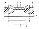
FIG. 21 shows an example of a cross-sectional structure of a conventional MOS transistor. As shown in this figure, an
[0003]
Next, a method for manufacturing the MOS transistor shown in FIG. 21 will be described with reference to FIGS. 22 and 23 are cross-sectional views showing characteristic first and second steps of the manufacturing process of the MOS transistor.
[0004]
First, a mask film (not shown) is formed on the main surface of
[0005]
Thereafter, as shown in FIG. 23, the
[0006]
Next, as shown in FIG. 21, an
[0007]
Next, another conventional example will be described with reference to FIGS. FIG. 24 is a cross-sectional structure diagram of an access MOS transistor portion and a driver MOS transistor portion in a conventional SRAM (Static Random Access Memory) memory cell.
[0008]
In general, in an SRAM memory cell, it is necessary to increase the current ratio between an access MOS transistor and a driver MOS transistor in order to stabilize the cell operation. The smaller the current value of the access MOS transistor is, the better the current value of the driver MOS transistor is.
[0009]
Therefore, the width Wd of the
[0010]
In addition, the following characteristics are required for SRAM memory cell transistors. In the access MOS transistor, it is desirable that the threshold voltage Vth at the time of back bias is low, and since the gate length is long, the channel dope implantation is preferably performed with low energy that suppresses the back bias effect.
[0011]
On the other hand, since the gate length of the driver MOS transistor is short, it is preferable to perform channel doping implantation with high energy in order to suppress punch-through.
[0012]
Next, a method of manufacturing the SRAM memory cell shown in FIG. 24 will be described. 25 and 26 are sectional views showing characteristic first and second steps of the manufacturing process of the SRAM memory cell shown in FIG.
[0013]
As in the case of the MOS transistor described above, a mask film is formed on the
[0014]
Next, as shown in FIG. 25, after forming an
[0015]
At this time, the thickness of the
[0016]
Next, as shown in FIG. 26,
[0017]
[Problems to be solved by the invention]
As described above, in the MOS transistor shown in FIG. 21, the
[0018]
Since the access MOS transistor and driver MOS transistor shown in FIG. 24 have the
[0019]
Furthermore, the thickness of the gate insulating films of the access MOS transistor and the driver MOS transistor cannot be changed without adding a separate step of forming an insulating film.
[0020]
That is, it is difficult to improve the performance of the memory cell in the SRAM without adding a new process and to stabilize the operation.
[0021]
The present invention has been made to solve the above problems. One object of the present invention is to reduce the leakage current of a semiconductor device having a MOS transistor. Another object of the present invention is to improve the performance of the memory cell in the SRAM and stabilize the operation without adding a new process.
[0037]
[Means for Solving the Problems]
A method for manufacturing a semiconductor device according to the present invention includes: A Access MOS transistor and driver MOS transistor SRAM with A method for manufacturing a semiconductor device having the following steps. The isolation region of the semiconductor substrate is exposed, and a first active region in which an access MOS transistor is formed and a second active region in which a driver MOS transistor is formed Respectively First on the semiconductor substrate to cover Mask film And a second mask film is formed. First Mask film And the second mask film are used to selectively oxidize the semiconductor substrate, thereby forming a bird's beak portion that covers the entire first active region and only the peripheral portion of the second active region. First Mask film And the second mask film after removing the first On the active area And first on the second active region Insulation film And a second insulating film are formed. Impurities are implanted into the first active region through the first insulating film and the bird's beak, and impurities are implanted into the second active region through the second insulating film. Then, channel doping is performed at a deep position in the second active region while channel doping is performed at a shallow position in the first active region. . First Insulation film And after removing the second insulating film, On the active area And on the second active region Respectively Third Insulation film And the first through the fourth insulating film Gate electrode And a second gate electrode are formed.
[0038]
By covering the entire first active region with the bird's beak as described above, the insulating film formed on the first active region when the first and second insulating films are formed on the first and second active regions Can be made larger than the thickness of the insulating film formed on the second active region. Since channel doping is performed through the underlying insulating film, the thickness of the underlying insulating film at the time of channel doping can be made larger on the first active region than on the second active region, and the channel doping depth in the first active region can be increased. The depth can be made shallower than that of the second active region. That is, the channel doping depth of the access MOS transistor can be made shallower than the channel doping depth of the driver MOS transistor. At this time, since it is only necessary to connect the bird's beaks on the first active region, it is not necessary to add a new process.
[0039]
The step of forming the bird's beak preferably includes the step of forming the bird's beak so that the surface of the first active region is entirely rounded by connecting the bird's beak on the first active region.
[0040]
Thereby, it is possible to suppress the occurrence of the recess portion at the edge of the isolation region around the access MOS transistor.
[0041]
The step of removing the first and second insulating films includes a step of exposing the surface of the second active region while leaving a bird's beak portion on the first active region.
[0042]
Thereby, the thickness of the gate insulating film of the access MOS transistor can be made substantially larger than the thickness of the gate insulating film of the driver MOS transistor, and the current value of the access MOS transistor can be reduced. As a result, the operation of the memory cell can be stabilized.
[0043]
DETAILED DESCRIPTION OF THE INVENTION
Hereinafter, embodiments of the present invention will be described with reference to FIGS.
[0044]
(Embodiment 1)
FIG. 1 is a cross-sectional view of the MOS transistor portion of the semiconductor device according to the first embodiment of the present invention. As shown in FIG. 1, the MOS transistor in the present embodiment is formed on an active region surrounded by an isolation region selectively provided on the main surface of a
[0045]
An isolation insulating film such as an
[0046]
As shown in FIG. 1, there is no recess portion at the edge of the
[0047]
Further, the surface of the active region located between the
[0048]
A channel doped
[0049]
Next, a method for manufacturing a semiconductor device in the present embodiment will be described with reference to FIGS. 2 to 7 are cross-sectional views showing the first to sixth steps of the semiconductor device manufacturing process according to the present embodiment.
[0050]
As shown in FIG. 2, a
[0051]
Next, the
[0052]
Next, the
[0053]
At this time, the length of the bird's
[0054]
For example, the field oxidation is H 2 , O 2 When performing in a gas at a temperature of 1050 ° C. for about 400 nm or less, the length of the bird's
[0055]
The material of the
[0056]
As shown in FIG. 4, the thickness of the bird's
[0057]
After removing the
[0058]
Next, as shown in FIG. 7, the
[0059]
Thereafter, an
[0060]
Next, a modification of the first embodiment will be described with reference to FIGS. FIG. 8 is a cross-sectional view of the MOS transistor portion in this modification.
[0061]
In the first embodiment, the case where the present invention is applied to the LOCOS type separation has been described. However, the idea of the present invention can also be applied to the trench type separation.
[0062]
As shown in FIG. 8, in this modification, a
[0063]
Next, the manufacturing method of this modification is demonstrated using FIG. 9 and FIG. 9 and 10 are cross-sectional views showing characteristic first and second steps in the manufacturing process of the present modification.
[0064]
First,
[0065]
Next, the resist
[0066]
Thereafter, the structure shown in FIG. 8 is obtained through the same steps as in the first embodiment.
(Embodiment 2)
Next, a second embodiment of the present invention will be described with reference to FIGS. FIG. 11 is a cross-sectional view showing an access MOS transistor portion and a driver MOS transistor portion in the semiconductor device of the second embodiment.
[0067]
In the second embodiment, the present invention is applied to an SRAM. The SRAM includes an access MOS transistor and a driver MOS transistor as shown in FIG. Then, the surface of the active region (hereinafter referred to as “first active region”) of the access MOS transistor formation portion is formed in a round shape that is convex upward as in the case of the first embodiment.
[0068]
Thereby, the thickness of the oxide film at the separation region edge can be increased, and the occurrence of the recess portion at the separation region edge can be suppressed as in the case of the first embodiment. Thereby, leakage current in the access MOS transistor can be suppressed.
[0069]
Further, the depth D1 of the
[0070]
Thereby, punch-through in the driver MOS transistor can be suppressed while suppressing the back bias effect of the access MOS transistor, and the performance of the memory cell can be improved.
[0071]
Further, the thickness t1 of the gate insulating film (the laminated film of the
[0072]
Also, the width W1 of the first active region is made smaller than the width W2 of the active region (hereinafter referred to as “second active region”) of the driver MOS transistor formation portion.
[0073]
Thereby, the current ratio between the access MOS transistor and the driver MOS transistor is increased to stabilize the memory cell operation, and the bird's
[0074]
Next, a method for manufacturing a semiconductor device according to the second embodiment will be described with reference to FIGS. 12 to 17 are cross-sectional views showing the first to sixth steps of the semiconductor device manufacturing process according to the second embodiment.
[0075]
As shown in FIG. 12, a
[0076]
Next, the
[0077]
Next, the
[0078]
Here, by making the first active region width W1 smaller than the second active region width W2 as described above, the bird's
[0079]
For example, when field oxidation is performed at about 400 nm or less under the same conditions as in the first embodiment, the first active region width W1 is set to 0.5 μm or less, and the second active region width W2 is set to about 0.7 μm or more. Thereby, the bird's
[0080]
By covering the entire first active region with the bird's
[0081]
Next, as shown in FIG. 15, the
[0082]
Next, as shown in FIG. 16, an
[0083]
At this time, impurities are implanted into the first active region through the
[0084]
Thereby, the depth D1 (for example, about 130 nm) of the channel doped
[0085]
Moreover, since it is only necessary to leave the bird's
[0086]
Next, as shown in FIG. 17, the
[0087]
In addition, since the thickness of
[0088]
Thereafter, an
[0089]
The idea of this embodiment can also be applied to trench isolation. FIG. 18 shows a structure of a modification applied to trench isolation.
[0090]
As shown in FIG. 18, in this modification, an
[0091]
Next, the manufacturing method of this modification is demonstrated using FIG. 19 and FIG.
As shown in FIG. 19,
[0092]
Next, resist
[0093]
Although the embodiment of the present invention has been described above, the embodiment disclosed this time should be considered as illustrative in all points and not restrictive. The scope of the present invention is defined by the terms of the claims, and includes meanings equivalent to the terms of the claims and all modifications within the scope.
[0096]
【The invention's effect】
The present invention Pertaining to According to the method of manufacturing a semiconductor device, the channel dope depth of the access MOS transistor is made shallower than that of the driver MOS transistor only by forming the bird's beak so as to cover the first active region which is the active region of the access MOS transistor. can do. Thereby, the performance of the SRAM memory cell can be improved without adding a new process.
[0097]
Further, when the above-described bird's beak portion covering the first active region is left, the thickness of the gate insulating film of the access MOS transistor is made larger than the thickness of the gate insulating film of the driver MOS transistor without adding a new process. Can be bigger. Therefore, the operation of the SRAM memory cell can be stabilized without adding a new process.
[Brief description of the drawings]
FIG. 1 is a cross-sectional view of a semiconductor device according to a first embodiment of the present invention.
2 is a cross-sectional view showing a first step of manufacturing the semiconductor device shown in FIG. 1; FIG.
3 is a cross-sectional view showing a second step of the manufacturing process of the semiconductor device shown in FIG. 1; FIG.
4 is a cross-sectional view showing a third step of the manufacturing process of the semiconductor device shown in FIG. 1; FIG.
FIG. 5 is a cross-sectional view showing a fourth step of the manufacturing process of the semiconductor device shown in FIG. 1;
6 is a cross-sectional view showing a fifth step of manufacturing the semiconductor device shown in FIG. 1; FIG.
7 is a cross-sectional view showing a sixth step of the manufacturing process of the semiconductor device shown in FIG. 1; FIG.
FIG. 8 is a cross-sectional view of a modification of the semiconductor device of FIG.
FIG. 9 is a cross-sectional view showing a characteristic first step in the manufacturing process of the semiconductor device shown in FIG. 8;
10 is a cross-sectional view showing a characteristic second step of the manufacturing process of the semiconductor device shown in FIG. 8; FIG.
FIG. 11 is a sectional view of a semiconductor device according to a second embodiment of the present invention.
12 is a cross-sectional view showing a first step of manufacturing the semiconductor device shown in FIG. 11. FIG.
13 is a cross-sectional view showing a second step of the manufacturing process of the semiconductor device shown in FIG. 11; FIG.
14 is a cross-sectional view showing a third step of the manufacturing process of the semiconductor device shown in FIG. 11; FIG.
15 is a cross-sectional view showing a fourth step of the manufacturing process of the semiconductor device shown in FIG. 11. FIG.
16 is a cross-sectional view showing a fifth step of manufacturing the semiconductor device shown in FIG. 11; FIG.
FIG. 17 is a cross-sectional view showing a sixth step of the manufacturing process of the semiconductor device shown in FIG. 11;
18 is a cross-sectional view of a variation of the semiconductor device shown in FIG.
FIG. 19 is a cross-sectional view showing a characteristic first step in the manufacturing process of the semiconductor device shown in FIG. 18;
20 is a cross-sectional view showing a characteristic second step of the manufacturing process of the semiconductor device shown in FIG. 18; FIG.
FIG. 21 is a cross-sectional view of a conventional semiconductor device.
22 is a cross-sectional view showing a characteristic first step in the manufacturing process of the semiconductor device shown in FIG. 21; FIG.
FIG. 23 is a cross-sectional view showing a characteristic second step of the manufacturing process of the semiconductor device shown in FIG. 21;
FIG. 24 is a cross-sectional view of another example of a conventional semiconductor device.
FIG. 25 is a cross-sectional view showing a characteristic first step in the manufacturing process of the semiconductor device shown in FIG. 24;
26 is a cross-sectional view showing a characteristic second step of the manufacturing process of the semiconductor device shown in FIG. 24;
[Explanation of symbols]
1 semiconductor substrate, 2 buffer film, 3 nitride film, 4 resist pattern, 5 isolation oxide film, 6 bird's beak part, 7, 8 oxide film, 9 gate electrode, 10 trench, 11 active region, 12 recess part, 13, 13a, 13b Channel doped region.
Claims (3)
半導体基板の分離領域を露出し、前記アクセスMOSトランジスタが形成される第1活性領域と、前記ドライバMOSトランジスタが形成される第2活性領域とをそれぞれ覆うように前記半導体基板上に第1マスク膜と第2マスク膜を形成する工程と、
前記第1マスク膜と第2マスク膜を用いて前記半導体基板を選択的に酸化することにより、前記第1活性領域全体を覆いかつ前記第2活性領域の周縁部のみを覆うバーズビーク部を形成する工程と、
前記第1マスク膜と第2マスク膜を除去した後に前記第1活性領域上と第2活性領域上に第1絶縁膜と第2絶縁膜をそれぞれ形成する工程と、
前記第1絶縁膜および前記バーズビーク部を通して前記第1活性領域に不純物を注入するとともに、前記第2絶縁膜を通して前記第2活性領域に不純物を注入して前記第1活性領域の浅い位置にチャネルドープを行ないながら、前記第2活性領域の深い位置にチャネルドープを行なう工程と、
前記第1絶縁膜と第2絶縁膜を除去した後に前記第1活性領域上と第2活性領域上にそれぞれ第3絶縁膜と第4絶縁膜を介して第1ゲート電極と第2ゲート電極を形成する工程と、
を備えた、半導体装置の製造方法。A method of manufacturing a semiconductor device having an SRAM including an access MOS (Metal Oxide Semiconductor) transistor and a driver MOS transistor,
Exposing the isolation region of the semiconductor substrate, the access to the first active region in which the MOS transistor is formed, the first mask layer and the second active region the driver MOS transistor is formed on the semiconductor substrate so as to cover each And forming a second mask film;
By selectively oxidizing the semiconductor substrate using the first mask film and the second mask film, a bird's beak portion is formed that covers the entire first active region and covers only the peripheral portion of the second active region. Process,
Forming a first insulating film and a second insulating film on the first active region and the second active region after removing the first mask film and the second mask film, respectively;
Impurities are implanted into the first active region through the first insulating film and the bird's beak portion, and impurities are implanted into the second active region through the second insulating film, and channel doping is performed at a shallow position of the first active region. Performing channel doping in a deep position of the second active region while performing
After removing the first insulating film and the second insulating film, a first gate electrode and a second gate electrode are formed on the first active region and the second active region via a third insulating film and a fourth insulating film, respectively . Forming, and
A method for manufacturing a semiconductor device, comprising:
Priority Applications (4)
| Application Number | Priority Date | Filing Date | Title |
|---|---|---|---|
| JP2001029779A JP4592193B2 (en) | 2001-02-06 | 2001-02-06 | Manufacturing method of semiconductor device |
| US09/909,975 US7061128B2 (en) | 2001-02-06 | 2001-07-23 | Semiconductor device and manufacturing method of the same |
| TW090122984A TW508797B (en) | 2001-02-06 | 2001-09-19 | Semiconductor device and manufacturing method of the same |
| KR10-2001-0058570A KR100438238B1 (en) | 2001-02-06 | 2001-09-21 | Semiconductor device and manufacturing method of the same |
Applications Claiming Priority (1)
| Application Number | Priority Date | Filing Date | Title |
|---|---|---|---|
| JP2001029779A JP4592193B2 (en) | 2001-02-06 | 2001-02-06 | Manufacturing method of semiconductor device |
Publications (3)
| Publication Number | Publication Date |
|---|---|
| JP2002231828A JP2002231828A (en) | 2002-08-16 |
| JP2002231828A5 JP2002231828A5 (en) | 2008-03-27 |
| JP4592193B2 true JP4592193B2 (en) | 2010-12-01 |
Family
ID=18894084
Family Applications (1)
| Application Number | Title | Priority Date | Filing Date |
|---|---|---|---|
| JP2001029779A Expired - Fee Related JP4592193B2 (en) | 2001-02-06 | 2001-02-06 | Manufacturing method of semiconductor device |
Country Status (4)
| Country | Link |
|---|---|
| US (1) | US7061128B2 (en) |
| JP (1) | JP4592193B2 (en) |
| KR (1) | KR100438238B1 (en) |
| TW (1) | TW508797B (en) |
Families Citing this family (5)
| Publication number | Priority date | Publication date | Assignee | Title |
|---|---|---|---|---|
| DE102004058468A1 (en) * | 2004-11-25 | 2006-06-01 | Atmel Germany Gmbh | Reduced kink effect MOS transistor and method of making the same |
| KR100680958B1 (en) * | 2005-02-23 | 2007-02-09 | 주식회사 하이닉스반도체 | Method for manufacturing PMOS transistor |
| KR100760910B1 (en) * | 2005-12-29 | 2007-09-21 | 동부일렉트로닉스 주식회사 | SRAM Device Having Common Contact |
| JP2017069231A (en) * | 2015-09-28 | 2017-04-06 | ソニー株式会社 | Mos field effect transistor, semiconductor integrated circuit, solid-state image sensor, and electronic apparatus |
| CN113130377A (en) * | 2021-04-14 | 2021-07-16 | 上海积塔半导体有限公司 | Method for reducing beak width of silicon local oxidation layer |
Citations (11)
| Publication number | Priority date | Publication date | Assignee | Title |
|---|---|---|---|---|
| JPH02246372A (en) * | 1989-03-20 | 1990-10-02 | Fujitsu Ltd | Semiconductor device and manufacture thereof |
| JPH053299A (en) * | 1991-02-08 | 1993-01-08 | Nec Corp | Static memory |
| JPH0536917A (en) * | 1991-07-30 | 1993-02-12 | Sony Corp | Manufacture of complementary semiconductor device |
| JPH05198570A (en) * | 1991-10-01 | 1993-08-06 | Hitachi Ltd | Semiconductor integrated circuit device and its manufacture |
| JPH06295999A (en) * | 1993-02-10 | 1994-10-21 | Mitsubishi Electric Corp | Semiconductor storage device and its manufacture |
| JPH09252129A (en) * | 1996-03-15 | 1997-09-22 | Sony Corp | Field-effect transistor and its manufacturing method |
| JPH1022403A (en) * | 1996-06-28 | 1998-01-23 | Toshiba Corp | Nonvolatile semiconductor storage device |
| JPH10144805A (en) * | 1996-11-08 | 1998-05-29 | Lg Semicon Co Ltd | Structure of transistor and fabrication thereof |
| JPH1140775A (en) * | 1997-07-23 | 1999-02-12 | Hitachi Ltd | Semiconductor device and its manufacture |
| JPH11274313A (en) * | 1998-03-26 | 1999-10-08 | Mitsubishi Electric Corp | Semiconductor device and its manufacture |
| JP2000174263A (en) * | 1998-12-07 | 2000-06-23 | Toshiba Corp | Semiconductor device and manufacture thereof |
Family Cites Families (12)
| Publication number | Priority date | Publication date | Assignee | Title |
|---|---|---|---|---|
| US5135882A (en) * | 1989-07-31 | 1992-08-04 | Micron Technology, Inc. | Technique for forming high-value inter-nodal coupling resistance for rad-hard applications in a double-poly, salicide process using local interconnect |
| JP3330962B2 (en) * | 1991-06-28 | 2002-10-07 | 同和鉱業株式会社 | Manufacturing method of oxide superconductor |
| KR970007589B1 (en) * | 1991-09-13 | 1997-05-10 | 니뽄 덴끼 가부시끼가이샤 | Static memory device |
| EP0560985A1 (en) * | 1991-10-01 | 1993-09-22 | Hitachi, Ltd. | Semiconductor integrated circuit device and manufacture thereof |
| KR100189727B1 (en) * | 1991-10-15 | 1999-06-01 | 구본준 | Method for expanding active-region and isolation of semiconductor device |
| US5358890A (en) * | 1993-04-19 | 1994-10-25 | Motorola Inc. | Process for fabricating isolation regions in a semiconductor device |
| JPH08111462A (en) * | 1994-10-12 | 1996-04-30 | Mitsubishi Electric Corp | Semiconductor memory and fabrication thereof |
| JP3400891B2 (en) * | 1995-05-29 | 2003-04-28 | 三菱電機株式会社 | Semiconductor storage device and method of manufacturing the same |
| US5650350A (en) * | 1995-08-11 | 1997-07-22 | Micron Technology, Inc. | Semiconductor processing method of forming a static random access memory cell and static random access memory cell |
| US5741737A (en) * | 1996-06-27 | 1998-04-21 | Cypress Semiconductor Corporation | MOS transistor with ramped gate oxide thickness and method for making same |
| KR100247933B1 (en) * | 1997-08-22 | 2000-03-15 | 윤종용 | Semiconductor device having butted contact and method for fabricating the same |
| JP3955404B2 (en) | 1998-12-28 | 2007-08-08 | 株式会社ルネサステクノロジ | Manufacturing method of semiconductor integrated circuit device |
-
2001
- 2001-02-06 JP JP2001029779A patent/JP4592193B2/en not_active Expired - Fee Related
- 2001-07-23 US US09/909,975 patent/US7061128B2/en not_active Expired - Fee Related
- 2001-09-19 TW TW090122984A patent/TW508797B/en not_active IP Right Cessation
- 2001-09-21 KR KR10-2001-0058570A patent/KR100438238B1/en not_active IP Right Cessation
Patent Citations (11)
| Publication number | Priority date | Publication date | Assignee | Title |
|---|---|---|---|---|
| JPH02246372A (en) * | 1989-03-20 | 1990-10-02 | Fujitsu Ltd | Semiconductor device and manufacture thereof |
| JPH053299A (en) * | 1991-02-08 | 1993-01-08 | Nec Corp | Static memory |
| JPH0536917A (en) * | 1991-07-30 | 1993-02-12 | Sony Corp | Manufacture of complementary semiconductor device |
| JPH05198570A (en) * | 1991-10-01 | 1993-08-06 | Hitachi Ltd | Semiconductor integrated circuit device and its manufacture |
| JPH06295999A (en) * | 1993-02-10 | 1994-10-21 | Mitsubishi Electric Corp | Semiconductor storage device and its manufacture |
| JPH09252129A (en) * | 1996-03-15 | 1997-09-22 | Sony Corp | Field-effect transistor and its manufacturing method |
| JPH1022403A (en) * | 1996-06-28 | 1998-01-23 | Toshiba Corp | Nonvolatile semiconductor storage device |
| JPH10144805A (en) * | 1996-11-08 | 1998-05-29 | Lg Semicon Co Ltd | Structure of transistor and fabrication thereof |
| JPH1140775A (en) * | 1997-07-23 | 1999-02-12 | Hitachi Ltd | Semiconductor device and its manufacture |
| JPH11274313A (en) * | 1998-03-26 | 1999-10-08 | Mitsubishi Electric Corp | Semiconductor device and its manufacture |
| JP2000174263A (en) * | 1998-12-07 | 2000-06-23 | Toshiba Corp | Semiconductor device and manufacture thereof |
Also Published As
| Publication number | Publication date |
|---|---|
| US7061128B2 (en) | 2006-06-13 |
| KR100438238B1 (en) | 2004-07-02 |
| KR20020065324A (en) | 2002-08-13 |
| TW508797B (en) | 2002-11-01 |
| US20020105098A1 (en) | 2002-08-08 |
| JP2002231828A (en) | 2002-08-16 |
Similar Documents
| Publication | Publication Date | Title |
|---|---|---|
| US6642125B2 (en) | Integrated circuits having adjacent P-type doped regions having shallow trench isolation structures without liner layers therein therebetween and methods of forming same | |
| JP2002198532A (en) | Semiconductor device having effective width of expanded active region and its manufacturing method | |
| JPH09129721A (en) | Manufacture of semiconductor device | |
| JP2000340791A (en) | Manufacturing method of semiconductor device | |
| US20020127818A1 (en) | Recess-free trench isolation structure and method of forming the same | |
| KR100507856B1 (en) | Method for fabricating MOS transistor | |
| JP2003017555A (en) | Semiconductor integrated circuit device and method of manufacturing same | |
| JP3604072B2 (en) | Method for manufacturing semiconductor device | |
| JPH1174508A (en) | Semiconductor device and its manufacture | |
| TW200529317A (en) | Semiconductor device with trench isolation structure and method for fabricating the same | |
| JP3744694B2 (en) | Semiconductor device manufacturing method for improving transistor characteristics | |
| US7259071B2 (en) | Semiconductor device with dual gate oxides | |
| JPH10242259A (en) | Semiconductor device and manufacture thereof | |
| JPH11145273A (en) | Manufacture of semiconductor device | |
| JP4592193B2 (en) | Manufacturing method of semiconductor device | |
| KR100361764B1 (en) | A method for forming a field oxide of a semiconductor device | |
| JPH1187697A (en) | Manufacture of semiconductor, manufacture of semiconductor memory, and semiconductor device | |
| KR100466207B1 (en) | Method for manufacturing a semiconductor device | |
| JP2707901B2 (en) | Method for manufacturing semiconductor device | |
| KR20010074389A (en) | Method of fabricating a MOS transistor in semiconductor devices | |
| JP2003332413A (en) | Semiconductor element isolation layer and method for forming insulated gate transistor | |
| JP2000150870A (en) | Semiconductor device and its manufacture | |
| JPH06244415A (en) | Semiconductor device and manufacture thereof | |
| KR20020016725A (en) | Method for isolating semiconductor devices | |
| JP2002124667A (en) | Method of manufacturing semiconductor device |
Legal Events
| Date | Code | Title | Description |
|---|---|---|---|
| A521 | Request for written amendment filed |
Free format text: JAPANESE INTERMEDIATE CODE: A523 Effective date: 20080205 |
|
| A621 | Written request for application examination |
Free format text: JAPANESE INTERMEDIATE CODE: A621 Effective date: 20080205 |
|
| A977 | Report on retrieval |
Free format text: JAPANESE INTERMEDIATE CODE: A971007 Effective date: 20100512 |
|
| A711 | Notification of change in applicant |
Free format text: JAPANESE INTERMEDIATE CODE: A712 Effective date: 20100519 |
|
| A131 | Notification of reasons for refusal |
Free format text: JAPANESE INTERMEDIATE CODE: A131 Effective date: 20100615 |
|
| A521 | Request for written amendment filed |
Free format text: JAPANESE INTERMEDIATE CODE: A523 Effective date: 20100812 |
|
| TRDD | Decision of grant or rejection written | ||
| A01 | Written decision to grant a patent or to grant a registration (utility model) |
Free format text: JAPANESE INTERMEDIATE CODE: A01 Effective date: 20100907 |
|
| A01 | Written decision to grant a patent or to grant a registration (utility model) |
Free format text: JAPANESE INTERMEDIATE CODE: A01 |
|
| A61 | First payment of annual fees (during grant procedure) |
Free format text: JAPANESE INTERMEDIATE CODE: A61 Effective date: 20100914 |
|
| FPAY | Renewal fee payment (event date is renewal date of database) |
Free format text: PAYMENT UNTIL: 20130924 Year of fee payment: 3 |
|
| R150 | Certificate of patent or registration of utility model |
Free format text: JAPANESE INTERMEDIATE CODE: R150 |
|
| LAPS | Cancellation because of no payment of annual fees |