JP4585745B2 - Method for forming a semiconductor device - Google Patents
Method for forming a semiconductor device Download PDFInfo
- Publication number
- JP4585745B2 JP4585745B2 JP2003167445A JP2003167445A JP4585745B2 JP 4585745 B2 JP4585745 B2 JP 4585745B2 JP 2003167445 A JP2003167445 A JP 2003167445A JP 2003167445 A JP2003167445 A JP 2003167445A JP 4585745 B2 JP4585745 B2 JP 4585745B2
- Authority
- JP
- Japan
- Prior art keywords
- layer
- material layer
- resist
- forming
- resist structure
- Prior art date
- Legal status (The legal status is an assumption and is not a legal conclusion. Google has not performed a legal analysis and makes no representation as to the accuracy of the status listed.)
- Expired - Fee Related
Links
Images


Classifications
-
- G—PHYSICS
- G03—PHOTOGRAPHY; CINEMATOGRAPHY; ANALOGOUS TECHNIQUES USING WAVES OTHER THAN OPTICAL WAVES; ELECTROGRAPHY; HOLOGRAPHY
- G03F—PHOTOMECHANICAL PRODUCTION OF TEXTURED OR PATTERNED SURFACES, e.g. FOR PRINTING, FOR PROCESSING OF SEMICONDUCTOR DEVICES; MATERIALS THEREFOR; ORIGINALS THEREFOR; APPARATUS SPECIALLY ADAPTED THEREFOR
- G03F7/00—Photomechanical, e.g. photolithographic, production of textured or patterned surfaces, e.g. printing surfaces; Materials therefor, e.g. comprising photoresists; Apparatus specially adapted therefor
- G03F7/0002—Lithographic processes using patterning methods other than those involving the exposure to radiation, e.g. by stamping
-
- B—PERFORMING OPERATIONS; TRANSPORTING
- B82—NANOTECHNOLOGY
- B82Y—SPECIFIC USES OR APPLICATIONS OF NANOSTRUCTURES; MEASUREMENT OR ANALYSIS OF NANOSTRUCTURES; MANUFACTURE OR TREATMENT OF NANOSTRUCTURES
- B82Y10/00—Nanotechnology for information processing, storage or transmission, e.g. quantum computing or single electron logic
-
- B—PERFORMING OPERATIONS; TRANSPORTING
- B82—NANOTECHNOLOGY
- B82Y—SPECIFIC USES OR APPLICATIONS OF NANOSTRUCTURES; MEASUREMENT OR ANALYSIS OF NANOSTRUCTURES; MANUFACTURE OR TREATMENT OF NANOSTRUCTURES
- B82Y40/00—Manufacture or treatment of nanostructures
-
- H—ELECTRICITY
- H01—ELECTRIC ELEMENTS
- H01L—SEMICONDUCTOR DEVICES NOT COVERED BY CLASS H10
- H01L21/00—Processes or apparatus adapted for the manufacture or treatment of semiconductor or solid state devices or of parts thereof
- H01L21/02—Manufacture or treatment of semiconductor devices or of parts thereof
- H01L21/027—Making masks on semiconductor bodies for further photolithographic processing not provided for in group H01L21/18 or H01L21/34
- H01L21/0271—Making masks on semiconductor bodies for further photolithographic processing not provided for in group H01L21/18 or H01L21/34 comprising organic layers
- H01L21/0273—Making masks on semiconductor bodies for further photolithographic processing not provided for in group H01L21/18 or H01L21/34 comprising organic layers characterised by the treatment of photoresist layers
-
- H—ELECTRICITY
- H01—ELECTRIC ELEMENTS
- H01L—SEMICONDUCTOR DEVICES NOT COVERED BY CLASS H10
- H01L21/00—Processes or apparatus adapted for the manufacture or treatment of semiconductor or solid state devices or of parts thereof
- H01L21/02—Manufacture or treatment of semiconductor devices or of parts thereof
- H01L21/027—Making masks on semiconductor bodies for further photolithographic processing not provided for in group H01L21/18 or H01L21/34
- H01L21/033—Making masks on semiconductor bodies for further photolithographic processing not provided for in group H01L21/18 or H01L21/34 comprising inorganic layers
- H01L21/0334—Making masks on semiconductor bodies for further photolithographic processing not provided for in group H01L21/18 or H01L21/34 comprising inorganic layers characterised by their size, orientation, disposition, behaviour, shape, in horizontal or vertical plane
- H01L21/0335—Making masks on semiconductor bodies for further photolithographic processing not provided for in group H01L21/18 or H01L21/34 comprising inorganic layers characterised by their size, orientation, disposition, behaviour, shape, in horizontal or vertical plane characterised by their behaviour during the process, e.g. soluble masks, redeposited masks
-
- H—ELECTRICITY
- H01—ELECTRIC ELEMENTS
- H01L—SEMICONDUCTOR DEVICES NOT COVERED BY CLASS H10
- H01L21/00—Processes or apparatus adapted for the manufacture or treatment of semiconductor or solid state devices or of parts thereof
- H01L21/02—Manufacture or treatment of semiconductor devices or of parts thereof
- H01L21/04—Manufacture or treatment of semiconductor devices or of parts thereof the devices having at least one potential-jump barrier or surface barrier, e.g. PN junction, depletion layer or carrier concentration layer
- H01L21/18—Manufacture or treatment of semiconductor devices or of parts thereof the devices having at least one potential-jump barrier or surface barrier, e.g. PN junction, depletion layer or carrier concentration layer the devices having semiconductor bodies comprising elements of Group IV of the Periodic System or AIIIBV compounds with or without impurities, e.g. doping materials
- H01L21/30—Treatment of semiconductor bodies using processes or apparatus not provided for in groups H01L21/20 - H01L21/26
- H01L21/302—Treatment of semiconductor bodies using processes or apparatus not provided for in groups H01L21/20 - H01L21/26 to change their surface-physical characteristics or shape, e.g. etching, polishing, cutting
- H01L21/306—Chemical or electrical treatment, e.g. electrolytic etching
- H01L21/308—Chemical or electrical treatment, e.g. electrolytic etching using masks
- H01L21/3083—Chemical or electrical treatment, e.g. electrolytic etching using masks characterised by their size, orientation, disposition, behaviour, shape, in horizontal or vertical plane
- H01L21/3085—Chemical or electrical treatment, e.g. electrolytic etching using masks characterised by their size, orientation, disposition, behaviour, shape, in horizontal or vertical plane characterised by their behaviour during the process, e.g. soluble masks, redeposited masks
Description
【0001】
【発明の属する技術分野】
本発明は包括的に半導体デバイスの分野に関し、より詳細には半導体デバイスを形成するための方法およびシステムに関する。
【0002】
【従来の技術】
現在、既存の構造を小型化するとともに、より小型の構造を製造する傾向が強くなっている。この工程は一般的に微細加工と呼ばれる。微細加工がかなりの影響力を持っている1つの分野は、マイクロエレクトロニクス分野である。詳細には、一般に超小型電子回路構造を小型化することにより、その構造のコストが下がり、性能が向上し、電力消費が減少し、さらに所与の寸法の場合に、より多くの部品を収容できるようなってきた。エレクトロニクス分野では、微細加工は多方面において盛んになっているが、バイオテクノロジー、光学、機械システム、センシング装置および原子炉のような他の応用形態にも適用されてきている。
【0003】
微細加工工程において用いられる1つの方法は、インプリントリソグラフィである。インプリントリソグラフィは通常、基板材料上の薄膜を高分解能でパターニングするために用いられる。パターニングされる薄膜には、誘電体、半導体、金属あるいは有機材料を用いることができ、その薄膜は薄膜あるいは個々の層としてパターニングされることができる。インプリントリソグラフィは、従来のフォトリソグラフィほど平坦性を気にしないので、ロールツーロール環境において素子をパターニングするのに特に有用である。さらに、インプリントリソグラフィはより高いスループットを有し、より幅が広い基板を取り扱うことができる。
【0004】
通常、電子回路素子の製造はいくつかのパターニングステップを必要とし、そのパターニングステップは多くの場合に、最小機構サイズに匹敵するか、さらにはそれを上回る精度で互いに位置合わせされなければならない。従来のフォトリソグラフィでは、光学的なアライメントマークを用いて、連続するパターニングステップ間の位置合わせを保証する。ロールツーロール方式でも光学的な位置合わせを用いることはできるが、いくつかの理由により実用的ではない。まず、根底となるインプリントリソグラフィ工程が光学的ではないため、位置合わせが複雑になる。次に、ロールツーロール方式の基板が平坦でないことにより、被写界深度の制限および他の光学収差に起因して、光学的に位置合わせを行うことができる精度に問題が生じる。最後に、ロールツーロール処理において用いられるフレキシブル基板は、温度、湿度あるいは機械的応力の変動に起因して、寸法の変化が生じる恐れがある。1つのパターニングされる層が次の層に対してこのように収縮あるいは拡大することにより、大きな面積の位置合わせが不可能になる場合がある。
【0005】
【発明が解決しようとする課題】
したがって、上記の問題を解消する、素子を製造するための方法およびシステムが必要とされる。その方法およびシステムは、簡単で、費用対効果があり、しかも既存の技術に容易に適応できなければならない。本発明の目的は、そのような方法およびシステムを提供することである。
【0006】
【課題を解決するための手段】
本発明は半導体デバイスを形成するための方法およびシステムを含む。本発明は、スタンピングツールを用いて、3次元レジスト構造を生成することを含み、それにより薄膜パターニングステップが一度の成形ステップでレジストに転写されることができ、その後、後続の処理ステップにおいて現れるようになる。したがって、連続するパターニングステップ間の位置合わせは、製造工程において発生する可能性がある拡大あるいは収縮に関係なく、スタンピングツールが製造された精度によって決定されることができる。
【0007】
本発明の第1の態様は、半導体デバイスを形成するための方法を含む。その方法は、基板を用意することと、基板上に第1の材料層を堆積することと、基板上に3次元(3D)レジスト構造を形成することとを含み、その3Dレジスト構造は、その構造全体にわたって複数の垂直方向に異なる高さを含む。
【0008】
本発明の第2の態様は、フレキシブル基板上に第1の材料層を堆積するための手段と、フレキシブル基板上にレジスト層を堆積するための手段と、レジスト層に3Dパターンを転写し、フレキシブル基板上に3Dレジスト層を形成するための手段と、その3Dレジスト層を用いてフレキシブル基板上に交点アレイを形成するための手段とを含む、半導体デバイスを形成するためのシステムを含む。
【0009】
本発明の他の態様および利点は、一例によって本発明の原理を例示する、添付の図面とともに取り上げられる、以下に記載される詳細な説明から明らかになるであろう。
【0010】
【発明の実施の形態】
本発明は半導体デバイスを形成するための方法およびシステムに関する。以下の説明は、当業者が本発明を実施し、利用できるようにするために提供され、特許出願およびその要件に即して与えられる。本明細書に記載される好ましい実施形態、ならびに一般的な原理および機構に対する種々の変更は、当業者には容易に明らかになるであろう。したがって、本発明は、示される実施形態に限定されることを意図するわけではなく、本明細書に記載される原理および機構に一致する最も広い範囲が認められるべきである。
【0011】
例示のための図面に示されるように、本発明は、半導体デバイスを形成するための方法およびシステムである。本発明は、スタンピングツールを用いて、3次元レジスト構造を生成することを含み、それによって、複数のパターンが一度の成形ステップでレジストに転写され、その後、後続の処理ステップにおいて現れるようになる。
【0012】
本発明は、半導体デバイスを形成するために用いられるものとして記載されているが、当業者であれば、本発明の精神および範囲内に留まりながら、本発明を用いて他のタイプの素子(たとえば、機械、光学、生物学等)を形成することができることは容易に理解されよう。
【0013】
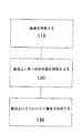
本発明をさらに深く理解するために、図1を参照されたい。図1は、本発明による方法の上位レベルの流れ図である。最初に、ステップ110によって、基板がおかれる。その基板は、ロールツーロール製造工程において用いるのに適したフレキシブル基板を含むことが好ましい。次に、ステップ120によって、基板上に材料層が堆積される。その材料は、有機材料あるいは無機材料を含むことが好ましい。最後に、ステップ130によって、第1の材料層上に、構造全体にわたって複数の垂直方向に異なる高さを含む3次元(3D)レジスト構造が形成される。その3Dレジスト構造は、スタンピングツールを用いることにより生成されることが好ましい。その3Dレジスト構造は構造全体にわたって複数の垂直方向に異なる高さを含むので、その構造を用いて、後続のエッチングステップに基づいて、下層にアライメントパターンを転写することができる。
【0014】
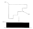
上記のように、本発明は、スタンピングツールを用いて、フレキシブル基板上の3Dレジスト構造を生成することを含む。この概念をより明瞭に理解するために、図2A〜図2Cを参照されたい。図2A〜図2Cは、スタンピングツールを用いて3Dレジスト構造を形成することに関する断面を示す。図2Aは、スタンピングツール210の断面と、未形成のレジスト材料層214とを示す。スタンピングツール210は、レジスト層214に転写されることになる3Dパターン212を含む。レジスト層214は、市販されている種々のポリマーのうちの任意のものを含むことができる。たとえば、ノーランド社光接着剤(NOA)ファミリのポリマーの中のものを用いることができる。
【0015】
その後、スタンピングツール210はレジスト層214に押圧され、それによりレジスト層214が変位し、スタンピングツール210の3Dパターン212が生成される。図2Bは、レジスト層214に押圧されているスタンピングツール210の断面を示す。その後、変位したレジスト層214は、紫外線リソグラフィあるいは他の適当な硬化手段を用いて硬化される。図2Cは形成されたレジスト層214’の断面を示す。
【0016】
さらに、図2Cから明らかなように、形成されたレジスト層214’、すなわちレジスト構造は、垂直方向に異なる高さ216、218、220、222を含む。垂直方向の高さは離散して異なる、すなわち少なくとも1つの高さが別の高さとは大きく異なることが好ましい。したがって、これらの垂直方向に異なる高さによって、構造214’は、後続のエッチングステップに基づいて、下層に対してアライメントパターンを転写するために用いられるようになる。これらの構造は、交点メモリアレイを形成する際に特に有用である。
【0017】
交点アレイ
交点メモリアレイは、その間に半導体層を有し、平行に離間して配列される直交する導体の組からなる2つの層を含むことが好ましい。2組の導体は行電極と列電極とを形成し、それらの電極は、行電極がそれぞれ厳密に1つの場所で各列電極を横切るように重ね合せられる。
【0018】
交点アレイをさらに詳しく理解するために、ここで図3を参照されたい。図3は交点アレイ構成300の図である。各交点では、半導体層330を通して行電極310と列電極320との間の接続が形成され、半導体層330は直列に接続されるダイオードおよびヒューズのように機能する。アレイ内のダイオードは全て、全ての行電極と全ての列電極との間に共通の電位がかけられる場合に、全てのダイオードに同じ方向にバイアスがかかるように向きを定められる。ヒューズ素子は、その中に臨界電流が流れる際に開回路になる分離素子として実現される場合があるか、あるいはダイオードの機能に組み込まれる場合がある。
【0019】
当業者であれば、上記の交点アレイが、本発明の精神および範囲内に留まりながら、限定はしないが、トランジスタ、抵抗、コンデンサ等を含む種々の半導体デバイスを形成する際に用いられ得ることができることは理解されよう。
【0020】
ここで、上記の3Dレジスト構造を用いて交点アレイを形成するために、3つの異なる手法が提供されるであろう。第1の手法は、3D構造とともに「シャドーイング」効果を利用して、交点アレイを形成する。第2の手法は、相互エッチング選択性を有する2つのポリマーを用いて、交点アレイを形成する。第3の手法は、毛管力の効果を利用して、3D構造を生成し、交点アレイを形成する。3つの手法が記載されるが、その3Dレジスト構造が、本発明の精神および範囲内に留まりながら、種々の異なる手法とともに利用できることは、当業者であれば理解されよう。
【0021】
シャドーイング効果
3Dレジスト構造を利用して交点アレイを形成するための第1の手法は、シャドーイング効果を考慮する。シャドーイング効果は、適当な条件下で、急勾配の側壁を有するトレンチを含むある表面上に薄膜が堆積される際に、堆積される材料が、堆積方向に垂直な表面上に優先的に集まり、側壁を覆うことが回避される現象である。ある角度で堆積し、それにより側壁の1つを「シャドーイングする」ことにより、多くの場合に、この効果を高めることができる。
【0022】
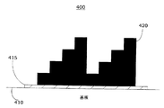
この手法においてシャドーイング効果が如何に考慮されるかをさらに深く理解するために、ここで、以下の説明とともに図4A〜図4Gを参照されたい。図4A〜図4Gは、シャドーイング効果を用いて交点アレイを形成する工程を示す。図4Aは、フレキシブル基板410と、第1の材料層(「第1の薄膜スタック」)415と、形成される3Dレジスト構造420とを含む構成400の側面図である。
【0023】
一旦、レジスト構造が形成されると、異方性エッチング工程によってレジスト構造の最も薄い層を除去し、それにより第1の薄膜スタックの一部を露出させることによりその工程が開始される。図4Bは、第1の薄膜スタックの露出された部分415’を示す。次に、同じあるいは異なるエッチング剤を用いて、第1の薄膜スタックの露出された部分がエッチングされ、それにより構造内に複数のポケットが形成される。図4Cは、エッチングされて基板410内にポケット425が形成された後の構成を示す。この工程において、ポケットの側壁は急峻なままであり、ポケットが第1の薄膜スタックの厚みよりも非常に大きな深さを有することが重要である。理想的には、「シャドーイング」効果を高めるために、基板内のポケットが第1の薄膜スタックをわずかにアンダーカットすることが最も望ましい。
【0024】
次に、レジスト構造のうちのその次に最も薄い層がエッチングされ、それにより第1の薄膜スタックの第2の部分が露出される。その後、第1の薄膜スタックの露出された第2の部分はエッチングされて貫通される。しかしながら、このステップでは、その下側にある基板から薄膜スタックが除去される際に、エッチングが停止される。図4Dは、このステップの後の露出された基板410’を示す。
【0025】
次のステップでは、レジスト構造のうちのその次に最も薄い部分がエッチングされ、それにより第1の薄膜スタックの第3の部分が露出される。しかしながら、このステップでは、第1の薄膜スタックの露出された部分はエッチングされない。このステップの終了時に、元のレジストの全ての残りの部分は一連の分離された島状部になる。図4Eは、レジストの分離された島状部430と、第1の薄膜スタックの露出された部分415’’とを示す。
【0026】
次に、その構成全体の上側に、第2の材料層(第2の薄膜スタック)が堆積される。第2の薄膜スタックは、半導体材料と導電性材料とを含むことが好ましい。これらの堆積の条件は、第1の薄膜スタックの厚みから生じる小さな段差部が、コンフォーマルに覆われるような条件になるであろう。しかしながら、ポケットの側壁に対応するより大きな段差部は覆われないであろう。図4Fは堆積後の第2の薄膜スタック435を示す。
【0027】
最後に、レジスト構造の残りの部分が除去され、それにより交点アレイが形成される。図4Gは交点アレイ440からなる構造を示す。このステップの終了時に、交点アレイが形成されているが、さらに別のステップとして、最終的な素子において短絡を引き起こす可能性がある、側壁上に残留する全ての薄膜を除去するための光洗浄が含まれる場合がある。
【0028】
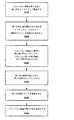
上記の手法をさらに深く理解するために、ここで図5を参照されたい。図5は、本発明による上記の方法の流れ図である。最初に、一旦、レジスト構造が形成されたなら、ステップ510によって、レジスト構造の第1の最も薄い層が異方性エッチングされ、それにより第1の薄膜スタックの第1の部分が露出される。次に、ステップ520によって、第1の薄膜スタックの露出された第1の部分がエッチングされ、基板内に複数のポケットが形成される。そのポケットは第1の薄膜スタックよりも非常に大きな深さを含み、第1の薄膜スタックをわずかにアンダーカットして、それによりシャドーイング効果を高めることが好ましい。次に、ステップ530によって、レジストの2番目に最も薄い層がエッチングされ、それにより、第1の薄膜スタックの第2の部分が露出される。
【0029】
その後、ステップ540によって、第1の薄膜スタックの露出された第2の部分がエッチングされる。その後、ステップ550によって、第2の薄膜スタックが堆積される。第2の薄膜スタックは、半導体材料と導電性材料とを含むことが好ましい。また、これらの堆積の条件は、第1の薄膜スタックの厚みから生じる小さな段差部が覆われ、ポケットの側壁に対応する、より大きな段差部が覆われないような条件である。最後に、ステップ560によって、レジストの残りの部分が除去される。
【0030】
相互エッチング選択性を有する2つのマスクポリマー
3Dレジスト構造を用いて交点アレイを形成するための第2の手法は、各化合物がある特定の条件下で他の化合物よりも非常に速くエッチングされることができ、たとえばポリマーAおよびBの場合に、ポリマー「A」のためのエッチングがポリマー「B」に影響を及ぼさず、ポリマー「B」のためのエッチングがポリマー「A」には影響を及ぼさないような特性を有する2つのポリマーを利用する。これらの条件は、異なるエッチング剤、異なる流速、異なる部分圧、異なるプラズマ電力等を含み得る。さらに、これらのエッチング方法はいずれも異方性ドライエッチングであることが好ましい。
【0031】
上記の手法はポリマー材料とともに用いられるものとして開示されるが、当業者であれば、本発明の精神および範囲内に留まりながら、成形され、鋳造され、その後硬化できる任意の材料が、ポリマー材料の代わりにレジストとして用いることができることは容易に理解されよう。たとえば、本発明の上記の実施形態において、スピン・オン・ガラス(SOG)を第2のポリマーとして用いることができる。
【0032】
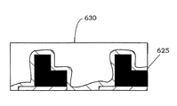
この手法についての理解をさらに深めるために、ここで、以下の説明とともに図6A〜図6Iを参照されたい。図6A〜図6Iは、2つのポリマーを用いて交点アレイを形成する工程を示す。図6Aは、フレキシブル基板610と、第1の材料層(「第1の薄膜スタック」)615と、形成された3Dレジスト構造620とを含む構成600を示しており、構造620全体にわたって、複数の垂直方向に異なる高さが存在する。一旦、レジスト構造が形成されたなら、レジスト構造の最も薄い層が異方性エッチング工程によって除去され、それにより第1の薄膜スタックの一部が露出される。図6Bは、第1の薄膜スタックの露出された部分615’を示す。
【0033】
次に、同じあるいは異なるエッチング剤を用いて、第1の薄膜スタックの露出された部分がエッチングされる。理想的には、これらのエッチング工程は、それらの工程がレジスト構造を腐蝕する速度以上の速度で第1の薄膜スタックを除去することになる。次に、レジスト構造のうちの次に薄い層がエッチングされ、それにより第1の薄膜スタックの第2の部分が露出され、その場合に、第1の薄膜スタックの第2の露出された部分は以前のステップにおいてエッチングされた領域に隣接して存在する。図6Cは第1の薄膜スタックの第2の露出された部分615’’を示す。
【0034】
次に、第2の材料層(第2の薄膜スタック)が堆積される。第2の薄膜スタックは半導体材料および導電性材料を含むことが好ましい。基板、第1の薄膜スタックおよびレジストの全ての露出された部分がこのステップにおいてコーティングされ得る。図6Dは堆積された第2の薄膜スタック625を示す。
【0035】
その後、第2のポリマーが第2の薄膜スタック上に被着される。このコーティングは、グラビアコーティングのようなロールコーティング工程によって被着され得るか、あるいは真空蒸着あるいは気相成長によって被着され得る。このコーティングは構造を平坦化することを意図しており、結果として、概ね平坦な表面が、先行するステップによって生成されたトポロジーの全てを覆うようになる。
図6Eは、第2の薄膜層625を覆う第2のポリマー層630を示す。
【0036】
次に、最初のレジストの水平な表面上に堆積された第2の薄膜スタックの全てが現れるまで、第2のポリマー層がエッチバックされる。図6Fは、第2のポリマー層630をエッチングした後に露出された第2の薄膜スタック625’を示す。第2の薄膜スタックは除去されることになるので、この工程のためのエッチング停止層として機能する必要はないことに留意されたい。
【0037】
次に、第2の薄膜スタックが、レジスト構造の上側表面からエッチングされる。ここで用いられるエッチング工程は、第2の薄膜スタックがエッチングされる速度より速く第2のポリマーを腐蝕しないことが重要である。図6Gは、第2の薄膜スタックがエッチングされた後のレジストの露出された部分620’を示す。次に、レジスト構造のうちの次に薄い部分がエッチングして除去され、それにより第1の薄膜スタックの別の部分が露出される。その後、第1の薄膜スタックのこの部分は、同じあるいは異なるエッチング剤によって除去される。レジストおよび第1の薄膜スタックを除去するために用いられる一連のエッチング工程は、第2のポリマーによって覆われる第2の薄膜スタックを除去しないことが好ましい。これは、第2のポリマー層あるいは第2の薄膜スタックの上層が第1の薄膜スタックおよびレジストを除去するエッチング工程に影響を受けないようにすることにより達成され得る。図6Hは、第2のポリマー層630の残りの部分を示す。
【0038】
最後に、レジスト構造および第2のポリマー層の残りの部分が除去され、それにより交点アレイが形成される。再び、さらに別のステップとして、最終的な素子において短絡を引き起こす可能性がある、側壁上に残留する全ての薄膜を除去するための光洗浄が含まれる場合がある。図6Iは、交点アレイ640からなる構造を示す。
【0039】
上記の手法の理解をさらに深めるために、ここで図7を参照されたい。図7は、本発明による上記の方法の流れ図である。最初に、一旦、レジスト構造が形成されたなら、ステップ705によって、そのレジスト構造の第1の最も薄い層が異方性エッチングされ、それにより第1の薄膜スタックの第1の部分が露出される。次に、ステップ710によって、第1の薄膜スタックの露出された第1の部分がエッチングされ、それにより基板の一部が露出される。その後、ステップ715によって、レジスト構造のうちの2番目に最も薄い層がエッチングされ、それにより第1の薄膜スタックの第2の部分が露出される。
【0040】
次に、ステップ720によって、第2の薄膜スタックが堆積される。第2の薄膜スタックは半導体材料と導電性材料とを含むことが好ましい。その後、ステップ725によって、第2の薄膜スタック上に第2のレジスト層が被着される。第2のレジスト層はロールコーティング工程によって被着できることが好ましい。次に、ステップ730によって、第2のレジスト層がエッチングされ、それにより第2の薄膜スタックの第1の部分が露出される。その後、ステップ735によって、第2の薄膜層のこの部分がエッチングされる。次に、ステップ740によって、レジストの3番目に最も薄い層がエッチングされ、それにより第1の薄膜スタックの第3の部分が露出される。その後、ステップ745によって、この露出された部分がエッチングされる。最後に、ステップ750によって、レジストおよび第2のレジスト層の残りの部分が除去される。
【0041】
毛管力
3Dレジスト構造を用いて交点アレイを形成するための第3の手法は、毛管力の現象を考慮する。毛管力は、レジスト材料が、幅が太い溝にではなく、細い溝により容易に入っていくようにする力である。この概念についての理解を深めるために、ここで図8を参照されたい。
【0042】
図8は、基板がフォトポリマーの薄い層でコーティングされ、その後、PDMS(ポリジメチルシロキサン)からなる紫外線透過性の型によって成形された実験の結果を示す。この例では、押型は、5.6μmの深さを有する、細い機構(10μm)および太い機構(100μm)を含んでいた。UV硬化性ポリマーの薄い層(0.9μm)が基板に被着された。押型が液体ポリマーに接触するとき、毛管力がポリマーの大部分を細い溝810に引き込み、太い領域820に入っていくポリマーは少なかった。また、それよりは多くのポリマーが、太い領域820の角部830に引き込まれた。
【0043】
より明確に理解するために、図9を参照されたい。図9は1つのトポロジーの図であり、それによれば、第1の機構910は第2の機構920より細い。第1の機構910が第2の機構920より細いので、毛管力によって、後続の堆積されるポリマー材料は、第2の機構920よりも第1の機構910により容易に入っていくようになる。結果として、第1の機構910が、第2の機構920のポリマー材料層よりも厚いポリマー材料層を含むことになるので、下側の材料が後続の処理ステップに基づいて容易にパターニングされることができる。
【0044】
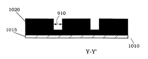
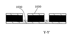
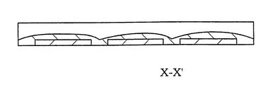
この手法をさらに深く理解するために、ここで、以下の説明とともに図10A〜図10Iを参照されたい。図10A〜図10Lは、毛管力を用いることにより交点アレイを形成する工程を示す。図10Aは、フレキシブル基板1010と、第1の材料層(「第1の薄膜スタック」)1015と、形成された3Dレジスト構造1020とを含む構成のX−X’ (図9より)断面図を示しており、構造1020全体にわたって、複数の垂直方向に異なる高さが存在する。図10Bは、その構成のY−Y’断面図を示す。両方の図面には、図9のトポロジーの機構910に対応する機構910も示される。
【0045】
一旦、レジスト構造が形成されたなら、そのレジスト構造のうちの最も薄い層が異方性エッチング工程によって除去され、それにより第1の薄膜スタックの一部が露出される。図10Cはその構成のX−X’断面図を示しており、それによれば第1の薄膜スタックの一部1015’が露出されている。図10Dは上記のエッチング工程後のその構成のY−Y’断面図を示す。
【0046】
次に、第2の材料層(第2の薄膜スタック)が堆積される。第2の薄膜スタックは半導体材料と導電性材料とを含むことが好ましい。図10Eおよび図10Fはそれぞれ、第2の薄膜スタック1030を堆積した後のその構成のX−X’およびY−Y’断面図を示す。
【0047】
その後、第2のポリマーがその構造全体にわたって被着される。第2のポリマーを被着する際に2つの技法が想定される。第1の技法を用いるとき、第2のポリマーは相対的に低い粘性を有し、容易にレジストを湿潤させる。被着される第2のポリマーの量は、その構造のトポロジー上に存在する空隙を完全に満たすほど十分な量ではないが、毛管力に起因して、第2のポリマーは細い通路により容易に入っていくであろう。結果として、これらの領域は、壁部間により大きな空間が存在する領域よりも深くまで満たされるであろう。
【0048】
第2の想定される技法は、気相成長あるいは真空蒸着工程を用いて、その構造上に均一に第2のポリマーを被着することを含む。再び、毛管力に基づいて、太い間隙よりも速く、細い間隙が隠されるであろう。また、この工程は幾何学的な効果に依存し、エッチング選択性には依存しないため、第2のポリマーはレジスト構造と同じあるいは異なる化学的組成を有する場合がある。図10Gおよび図10Hはそれぞれ、第2のポリマー1040を堆積した後のその構成のX−X’およびY−Y’断面図を示す。
【0049】
上記の手法はポリマー材料とともに利用されるものとして開示されるが、当業者であれば、本発明の精神および範囲内に留まりながら、種々のレジスト化合物のうちの任意の化合物を用いることができることは容易に理解されよう。
【0050】
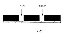
一旦、第2のポリマーが被着されたなら、異方性エッチングが実行され、それにより露出された第2の薄膜スタックが除去され、第1のレジストの一部が露出される。図10Iおよび図10Jはそれぞれ、異方性エッチングが実行された後のその構成のX−X’およびY−Y’断面図を示す。図10Jは露出されたレジスト1020’を示す。次に、レジストおよび第2のポリマーが除去される。第2の薄膜スタックが第1の薄膜スタックを覆う領域が交点アレイである。図10Kおよび図10Lはそれぞれ、形成された交点アレイ1050のX−X’およびY−Y’断面図を示す。
【0051】
上記の手法をより深く理解するために、ここで図11を参照されたい。図11は、本発明による上記の方法の流れ図である。最初に、一旦、レジスト構造が形成されたなら、ステップ1100によって、そのレジスト構造の第1の最も薄い層が異方性エッチングされ、それにより第1の薄膜スタックの第1の部分が露出される。形成されるレジスト構造は、別の機構より幅が広い少なくとも1つの機構を含むことが好ましい。その後、ステップ1110によって、第2の薄膜スタックが堆積される。第2の薄膜スタックは半導体材料および導電性材料を含むことが好ましい。
【0052】
次に、ステップ1120によって、第2のポリマー層が堆積される。その後、ステップ1130によって、異方性エッチングが実行され、それにより第2の薄膜スタックが除去されて、レジストの一部が露出される。最後に、ステップ1140によって、レジストおよび第2のポリマーの残りの部分が除去される。
【0053】
半導体デバイスを形成するための方法およびシステムが開示されてきた。その方法およびシステムは、スタンピングツールを用いて3Dレジスト構造を生成することを含み、それにより薄膜パターンが一度の成形ステップでレジストに転写され、その後、後続の処理ステップにおいて現れるようになる。
【0054】
本発明が図示される実施形態にしたがって記載されてきたが、当業者であれば、それらの実施形態に対する変形形態が実現可能であり、それらの変形形態が本発明の精神および範囲内に入ることは容易に理解されよう。したがって、併記の特許請求の範囲の精神および範囲から逸脱することなく、数多くの変更が当業者によってなされる場合がある。
【0055】
【発明の効果】
本発明によれば、半導体デバイスの製造時に、基板の拡大あるいは縮小に関係なく薄膜のパターニングステップ間の位置ずれが生じることのない、簡単で、費用対効果があり、しかも既存の技術に容易に適応する半導体微細加工方法およびシステムを提供することである。
【図面の簡単な説明】
【図1】本発明による方法の上位レベルの流れ図。
【図2A】スタンピングツールを用いる3Dレジスト構造の形成を示す図。
【図2B】スタンピングツールを用いる3Dレジスト構造の形成を示す図。
【図2C】スタンピングツールを用いる3Dレジスト構造の形成を示す図。
【図3】交点アレイ構成の図。
【図4A】シャドーイング効果を用いて交点アレイを形成する、第1の実施形態における一段階を示す図。
【図4B】シャドーイング効果を用いて交点アレイを形成する、第1の実施形態における一段階を示す図。
【図4C】シャドーイング効果を用いて交点アレイを形成する、第1の実施形態における一段階を示す図。
【図4D】シャドーイング効果を用いて交点アレイを形成する、第1の実施形態における一段階を示す図。
【図4E】シャドーイング効果を用いて交点アレイを形成する、第1の実施形態における一段階を示す図。
【図4F】シャドーイング効果を用いて交点アレイを形成する、第1の実施形態における一段階を示す図。
【図4G】シャドーイング効果を用いて交点アレイを形成する、第1の実施形態における一段階を示す図。
【図5】本発明による方法の第1の実施形態の流れ図。
【図6A】2つのポリマーを用いて交点アレイを形成する、第2の実施形態における一段階を示す図。
【図6B】2つのポリマーを用いて交点アレイを形成する、第2の実施形態における一段階を示す図。
【図6C】2つのポリマーを用いて交点アレイを形成する、第2の実施形態における一段階を示す図。
【図6D】2つのポリマーを用いて交点アレイを形成する、第2の実施形態における一段階を示す図。
【図6E】2つのポリマーを用いて交点アレイを形成する、第2の実施形態における一段階を示す図。
【図6F】2つのポリマーを用いて交点アレイを形成する、第2の実施形態における一段階を示す図。
【図6G】2つのポリマーを用いて交点アレイを形成する、第2の実施形態における一段階を示す図。
【図6H】2つのポリマーを用いて交点アレイを形成する、第2の実施形態における一段階を示す図。
【図6I】2つのポリマーを用いて交点アレイを形成する、第2の実施形態における一段階を示す図。
【図7】本発明による方法の第2の実施形態の流れ図。
【図8】基板がフォトポリマーの薄い層でコーティングされ、次にPDMSの紫外線透過性の型によって成形された実験の結果を示す図。
【図9】第1の機構が第2の機構よりも狭いトポロジーを示す図。
【図10A】毛管力を用いることにより交点アレイを形成する、第3の実施形態における一段階を示す図。
【図10B】毛管力を用いることにより交点アレイを形成する、第3の実施形態における一段階を示す図。
【図10C】毛管力を用いることにより交点アレイを形成する、第3の実施形態における一段階を示す図。
【図10D】毛管力を用いることにより交点アレイを形成する、第3の実施形態における一段階を示す図。
【図10E】毛管力を用いることにより交点アレイを形成する、第3の実施形態における一段階を示す図。
【図10F】毛管力を用いることにより交点アレイを形成する、第3の実施形態における一段階を示す図。
【図10G】毛管力を用いることにより交点アレイを形成する、第3の実施形態における一段階を示す図。
【図10H】毛管力を用いることにより交点アレイを形成する、第3の実施形態における一段階を示す図。
【図10I】毛管力を用いることにより交点アレイを形成する、第3の実施形態における一段階を示す図。
【図10J】毛管力を用いることにより交点アレイを形成する、第3の実施形態における一段階を示す図。
【図10K】毛管力を用いることにより交点アレイを形成する、第3の実施形態における一段階を示す図。
【図10L】毛管力を用いることにより交点アレイを形成する、第3の実施形態における一段階を示す図。
【図11】本発明による方法の第3の実施形態の流れ図。
【符号の説明】
210 スタンピングツール
212 3Dパターン
214 レジスト層
300 交点アレイ
310 行電極
320 列電極
410 フレキシブル基盤
420 3Dレジスト構造[0001]
BACKGROUND OF THE INVENTION
The present invention relates generally to the field of semiconductor devices, and more particularly to methods and systems for forming semiconductor devices.
[0002]
[Prior art]
Currently, there is an increasing trend to produce smaller structures while miniaturizing existing structures. This process is generally called microfabrication. One area where microfabrication has a considerable impact is in the microelectronics field. Specifically, miniaturization of microelectronic circuit structures generally reduces the cost of the structure, improves performance, reduces power consumption, and accommodates more components for a given size I'm able to do it. In the electronics field, microfabrication has flourished in many fields, but has also been applied to other applications such as biotechnology, optics, mechanical systems, sensing devices and nuclear reactors.
[0003]
One method used in the microfabrication process is imprint lithography. Imprint lithography is typically used to pattern a thin film on a substrate material with high resolution. The thin film to be patterned can be a dielectric, semiconductor, metal or organic material, and the thin film can be patterned as a thin film or as individual layers. Imprint lithography is particularly useful for patterning devices in a roll-to-roll environment because it is not as flat as conventional photolithography. Furthermore, imprint lithography has a higher throughput and can handle wider substrates.
[0004]
Typically, the fabrication of electronic circuit elements requires several patterning steps, which often have to be aligned with each other with an accuracy comparable to or even greater than the minimum feature size. In conventional photolithography, optical alignment marks are used to ensure alignment between successive patterning steps. Although roll-to-roll can also use optical alignment, it is not practical for several reasons. First, alignment is complicated because the underlying imprint lithography process is not optical. Next, since the roll-to-roll substrate is not flat, there is a problem in the accuracy with which optical alignment can be performed due to the limitation of the depth of field and other optical aberrations. Finally, flexible substrates used in roll-to-roll processing can undergo dimensional changes due to variations in temperature, humidity or mechanical stress. Larger area alignment may not be possible if one layer to be patterned shrinks or expands in this manner relative to the next layer.
[0005]
[Problems to be solved by the invention]
Therefore, there is a need for a method and system for manufacturing devices that eliminates the above problems. The method and system must be simple, cost-effective and easily adaptable to existing technologies. An object of the present invention is to provide such a method and system.
[0006]
[Means for Solving the Problems]
The present invention includes methods and systems for forming semiconductor devices. The present invention includes using a stamping tool to generate a three-dimensional resist structure so that the thin film patterning step can be transferred to the resist in a single molding step, and then appear in subsequent processing steps. become. Thus, the alignment between successive patterning steps can be determined by the accuracy with which the stamping tool is manufactured, regardless of the expansion or contraction that may occur in the manufacturing process.
[0007]
A first aspect of the invention includes a method for forming a semiconductor device. The method includes providing a substrate, depositing a first material layer on the substrate, and forming a three-dimensional (3D) resist structure on the substrate, the 3D resist structure comprising: Includes a plurality of vertically different heights throughout the structure.
[0008]
According to a second aspect of the present invention, there is provided a means for depositing a first material layer on a flexible substrate, a means for depositing a resist layer on the flexible substrate, a 3D pattern transferred to the resist layer, and a flexible A system for forming a semiconductor device is included that includes means for forming a 3D resist layer on a substrate and means for forming an array of intersections on a flexible substrate using the 3D resist layer.
[0009]
Other aspects and advantages of the present invention will become apparent from the following detailed description, taken in conjunction with the accompanying drawings, illustrating by way of example the principles of the invention.
[0010]
DETAILED DESCRIPTION OF THE INVENTION
The present invention relates to methods and systems for forming semiconductor devices. The following description is provided to enable one of ordinary skill in the art to make and use the invention and is provided in the context of a patent application and its requirements. Various modifications to the preferred embodiments and general principles and mechanisms described herein will be readily apparent to those skilled in the art. Accordingly, the present invention is not intended to be limited to the embodiments shown, but is to be accorded the widest scope consistent with the principles and mechanisms described herein.
[0011]
As shown in the drawings for purposes of illustration, the present invention is a method and system for forming a semiconductor device. The present invention includes using a stamping tool to generate a three-dimensional resist structure, whereby multiple patterns are transferred to the resist in a single molding step and then appear in subsequent processing steps.
[0012]
Although the present invention has been described as being used to form a semiconductor device, those skilled in the art will recognize that other types of elements (e.g., using the present invention while remaining within the spirit and scope of the present invention) It will be readily understood that a machine, optics, biology, etc.) can be formed.
[0013]
For a better understanding of the present invention, please refer to FIG. FIG. 1 is a high-level flowchart of the method according to the invention. Initially,
[0014]
As described above, the present invention includes generating a 3D resist structure on a flexible substrate using a stamping tool. For a clearer understanding of this concept, please refer to FIGS. 2A-2C. 2A-2C show cross sections for forming a 3D resist structure using a stamping tool. FIG. 2A shows a cross section of the
[0015]
Thereafter, the
[0016]
Further, as is apparent from FIG. 2C, the formed resist
[0017]
Intersection array
The intersection memory array preferably includes two layers of sets of orthogonal conductors spaced apart in parallel with a semiconductor layer therebetween. The two sets of conductors form a row electrode and a column electrode, which are superimposed such that each row electrode traverses each column electrode at exactly one location.
[0018]
For a more detailed understanding of the intersection array, refer now to FIG. FIG. 3 is a diagram of an
[0019]
Those skilled in the art will appreciate that the intersection array described above can be used in forming a variety of semiconductor devices including, but not limited to, transistors, resistors, capacitors, etc., while remaining within the spirit and scope of the present invention. It will be understood that it can be done.
[0020]
Here, three different approaches will be provided to form intersection arrays using the 3D resist structure described above. The first approach uses the “shadowing” effect with the 3D structure to form the intersection array. The second approach uses two polymers with mutual etch selectivity to form an intersection array. The third technique uses the effect of capillary forces to generate 3D structures and form intersection arrays. Although three approaches are described, those skilled in the art will appreciate that the 3D resist structure can be used with a variety of different approaches while remaining within the spirit and scope of the present invention.
[0021]
Shadowing effect
A first technique for forming an intersection array using a 3D resist structure takes into account the shadowing effect. The shadowing effect is that, under appropriate conditions, when a thin film is deposited on a surface containing a trench with steep sidewalls, the deposited material preferentially collects on the surface perpendicular to the deposition direction. This is a phenomenon in which covering the side wall is avoided. This effect can often be enhanced by depositing at an angle, thereby "shadowing" one of the side walls.
[0022]
To better understand how shadowing effects are considered in this approach, please refer now to FIGS. 4A-4G along with the following description. 4A-4G show the process of forming an intersection array using the shadowing effect. FIG. 4A is a side view of an
[0023]
Once the resist structure is formed, the process is initiated by removing the thinnest layer of the resist structure by an anisotropic etching process, thereby exposing a portion of the first thin film stack. FIG. 4B shows the exposed
[0024]
Next, the next thinnest layer of the resist structure is etched, thereby exposing the second portion of the first thin film stack. Thereafter, the exposed second portion of the first thin film stack is etched through. However, in this step, the etching is stopped when the thin film stack is removed from the underlying substrate. FIG. 4D shows the exposed
[0025]
In the next step, the next thinnest portion of the resist structure is etched, thereby exposing the third portion of the first thin film stack. However, in this step, the exposed portion of the first thin film stack is not etched. At the end of this step, all remaining portions of the original resist become a series of isolated islands. FIG. 4E shows the
[0026]
Next, a second material layer (second thin film stack) is deposited above the entire configuration. The second thin film stack preferably includes a semiconductor material and a conductive material. These deposition conditions will be such that small steps resulting from the thickness of the first thin film stack are conformally covered. However, the larger step corresponding to the side wall of the pocket will not be covered. FIG. 4F shows the second
[0027]
Finally, the remaining portion of the resist structure is removed, thereby forming an intersection array. FIG. 4G shows a structure consisting of
[0028]
To better understand the above approach, please refer now to FIG. FIG. 5 is a flowchart of the above method according to the present invention. Initially, once the resist structure is formed, step 510 anisotropically etches the first thinnest layer of the resist structure, thereby exposing the first portion of the first thin film stack. Next, step 520 etches the exposed first portion of the first thin film stack to form a plurality of pockets in the substrate. The pocket preferably includes a much greater depth than the first thin film stack, and the first thin film stack is preferably slightly undercut, thereby enhancing the shadowing effect. Next, step 530 etches the second thinnest layer of resist, thereby exposing the second portion of the first thin film stack.
[0029]
Thereafter, step 540 etches the exposed second portion of the first thin film stack. Thereafter, step 550 deposits a second thin film stack. The second thin film stack preferably includes a semiconductor material and a conductive material. These deposition conditions are such that a small step portion resulting from the thickness of the first thin film stack is covered and a larger step portion corresponding to the side wall of the pocket is not covered. Finally,
[0030]
Two mask polymers with mutual etch selectivity
A second approach to forming intersection arrays using 3D resist structures allows each compound to be etched much faster than other compounds under certain conditions, such as for polymers A and B In addition, two polymers having characteristics such that etching for polymer “A” does not affect polymer “B” and etching for polymer “B” does not affect polymer “A” are utilized. To do. These conditions can include different etchants, different flow rates, different partial pressures, different plasma powers, and the like. Furthermore, it is preferable that any of these etching methods is anisotropic dry etching.
[0031]
While the above approach is disclosed for use with a polymeric material, those skilled in the art will recognize that any material that can be molded, cast, and subsequently cured while remaining within the spirit and scope of the present invention. It will be readily appreciated that it can be used as a resist instead. For example, in the above embodiment of the present invention, spin-on glass (SOG) can be used as the second polymer.
[0032]
To further understand this approach, please refer now to FIGS. 6A-6I along with the following discussion. 6A-6I illustrate the process of forming an intersection array using two polymers. FIG. 6A shows a
[0033]
The exposed portion of the first thin film stack is then etched using the same or different etchant. Ideally, these etch steps will remove the first thin film stack at a rate that is greater than the rate at which they etch the resist structure. Next, the next thin layer of the resist structure is etched, thereby exposing the second portion of the first thin film stack, in which case the second exposed portion of the first thin film stack is Present adjacent to the area etched in the previous step. FIG. 6C shows a second exposed
[0034]
Next, a second material layer (second thin film stack) is deposited. The second thin film stack preferably includes a semiconductor material and a conductive material. All exposed portions of the substrate, first thin film stack and resist can be coated in this step. FIG. 6D shows the deposited second
[0035]
A second polymer is then deposited on the second thin film stack. This coating can be applied by a roll coating process such as gravure coating, or by vacuum evaporation or vapor deposition. This coating is intended to planarize the structure, resulting in a generally flat surface covering all of the topology generated by the previous step.
FIG. 6E shows a
[0036]
Next, the second polymer layer is etched back until all of the second thin film stack deposited on the horizontal surface of the initial resist appears. FIG. 6F shows the second
[0037]
Next, the second thin film stack is etched from the upper surface of the resist structure. It is important that the etching process used here does not corrode the second polymer faster than the rate at which the second thin film stack is etched. FIG. 6G shows the exposed
[0038]
Finally, the resist structure and the remaining portion of the second polymer layer are removed, thereby forming an intersection array. Again, yet another step may include light cleaning to remove any thin film remaining on the sidewalls that can cause a short circuit in the final device. FIG. 6I shows a structure consisting of
[0039]
To better understand the above approach, please refer now to FIG. FIG. 7 is a flowchart of the above method according to the present invention. Initially, once the resist structure has been formed, step 705 anisotropically etches the first thinnest layer of the resist structure, thereby exposing the first portion of the first thin film stack. . Next, step 710 etches the exposed first portion of the first thin film stack, thereby exposing a portion of the substrate. Thereafter, step 715 etches the second thinnest layer of the resist structure, thereby exposing the second portion of the first thin film stack.
[0040]
Next, step 720 deposits a second thin film stack. The second thin film stack preferably includes a semiconductor material and a conductive material. Thereafter, in
[0041]
Capillary force
A third approach for forming an intersection array using a 3D resist structure takes into account the phenomenon of capillary forces. Capillary force is the force that allows the resist material to enter easily through narrow grooves rather than into wide grooves. To better understand this concept, refer now to FIG.
[0042]
FIG. 8 shows the results of an experiment in which the substrate was coated with a thin layer of photopolymer and then molded with a UV transmissive mold consisting of PDMS (polydimethylsiloxane). In this example, the mold included a thin feature (10 μm) and a thick feature (100 μm) with a depth of 5.6 μm. A thin layer (0.9 μm) of UV curable polymer was deposited on the substrate. When the mold contacted the liquid polymer, the capillary force pulled most of the polymer into the
[0043]
For a clearer understanding, please refer to FIG. FIG. 9 is a diagram of one topology, according to which the
[0044]
To better understand this approach, please refer now to FIGS. 10A-10I along with the following description. 10A-10L illustrate the process of forming an intersection array by using capillary forces. FIG. 10A shows a cross-sectional view of XX ′ (from FIG. 9) of a configuration including a
[0045]
Once the resist structure is formed, the thinnest layer of the resist structure is removed by an anisotropic etching process, thereby exposing a portion of the first thin film stack. FIG. 10C shows an XX ′ cross-sectional view of the configuration, whereby a
[0046]
Next, a second material layer (second thin film stack) is deposited. The second thin film stack preferably includes a semiconductor material and a conductive material. FIGS. 10E and 10F show XX ′ and YY ′ cross-sectional views of the configuration after the second
[0047]
A second polymer is then applied over the entire structure. Two techniques are envisioned in applying the second polymer. When using the first technique, the second polymer has a relatively low viscosity and easily wets the resist. The amount of second polymer deposited is not sufficient to completely fill the voids present on the topological structure of the structure, but due to capillary forces, the second polymer is more easily accommodated by narrow passages. Will enter. As a result, these areas will be filled deeper than areas where there is more space between the walls.
[0048]
A second envisioned technique involves depositing the second polymer uniformly on the structure using a vapor deposition or vacuum deposition process. Again, based on capillary forces, narrow gaps will be hidden faster than thick gaps. Also, since this process depends on geometric effects and not on etch selectivity, the second polymer may have the same or different chemical composition as the resist structure. FIGS. 10G and 10H respectively show XX ′ and YY ′ cross-sectional views of the configuration after the
[0049]
While the above approach is disclosed as being utilized with polymeric materials, those skilled in the art will be able to use any of a variety of resist compounds while remaining within the spirit and scope of the present invention. Easy to understand.
[0050]
Once the second polymer has been deposited, an anisotropic etch is performed, thereby removing the exposed second thin film stack and exposing a portion of the first resist. FIGS. 10I and 10J respectively show XX ′ and YY ′ cross-sectional views of the configuration after anisotropic etching has been performed. FIG. 10J shows the exposed resist 1020 ′. Next, the resist and the second polymer are removed. The area where the second thin film stack covers the first thin film stack is the intersection array. FIGS. 10K and 10L show XX ′ and YY ′ cross-sectional views of the formed
[0051]
To better understand the above approach, please refer now to FIG. FIG. 11 is a flowchart of the above method according to the present invention. Initially, once the resist structure is formed,
[0052]
Next, according to
[0053]
A method and system for forming a semiconductor device has been disclosed. The method and system includes generating a 3D resist structure using a stamping tool so that the thin film pattern is transferred to the resist in a single molding step and then appears in subsequent processing steps.
[0054]
Although the present invention has been described in accordance with the illustrated embodiments, those skilled in the art will appreciate that variations to those embodiments are possible and that these variations are within the spirit and scope of the present invention. Will be easily understood. Accordingly, many modifications may be made by one of ordinary skill in the art without departing from the spirit and scope of the appended claims.
[0055]
【The invention's effect】
In accordance with the present invention, a simple, cost-effective, and easy to existing technology does not cause misalignment between thin film patterning steps regardless of substrate enlargement or reduction during semiconductor device manufacturing. To provide an adaptive semiconductor microfabrication method and system.
[Brief description of the drawings]
FIG. 1 is a high-level flowchart of a method according to the invention.
FIG. 2A illustrates the formation of a 3D resist structure using a stamping tool.
FIG. 2B shows the formation of a 3D resist structure using a stamping tool.
FIG. 2C illustrates the formation of a 3D resist structure using a stamping tool.
FIG. 3 is a diagram of an intersection array configuration.
FIG. 4A is a diagram illustrating a stage in the first embodiment of forming an intersection array using the shadowing effect.
FIG. 4B is a diagram illustrating a stage in the first embodiment of forming an intersection array using the shadowing effect.
FIG. 4C is a diagram illustrating a stage in the first embodiment of forming an intersection array using the shadowing effect.
FIG. 4D shows a step in the first embodiment of forming an intersection array using the shadowing effect.
FIG. 4E shows a step in the first embodiment of forming an intersection array using the shadowing effect.
FIG. 4F shows a step in the first embodiment of forming an intersection array using the shadowing effect.
FIG. 4G is a diagram showing a stage in the first embodiment of forming an intersection array using the shadowing effect.
FIG. 5 is a flow chart of a first embodiment of the method according to the invention.
FIG. 6A shows a step in a second embodiment in which two polymers are used to form an intersection array.
FIG. 6B shows a step in the second embodiment in which two polymers are used to form an intersection array.
FIG. 6C shows a step in the second embodiment in which two polymers are used to form an intersection array.
FIG. 6D shows a step in the second embodiment in which two polymers are used to form an intersection array.
FIG. 6E shows a step in the second embodiment in which two polymers are used to form an intersection array.
FIG. 6F shows a step in the second embodiment in which two polymers are used to form an intersection array.
FIG. 6G shows a step in the second embodiment in which two polymers are used to form an intersection array.
FIG. 6H shows a step in the second embodiment in which two polymers are used to form an intersection array.
FIG. 6I shows a step in the second embodiment in which two polymers are used to form an intersection array.
FIG. 7 is a flow chart of a second embodiment of the method according to the invention.
FIG. 8 shows the results of an experiment in which a substrate was coated with a thin layer of photopolymer and then molded with a PDMS UV transparent mold.
FIG. 9 is a diagram showing a topology in which the first mechanism is narrower than the second mechanism.
FIG. 10A shows a step in a third embodiment of forming an intersection array by using capillary forces.
FIG. 10B shows a step in the third embodiment of forming an intersection array by using capillary forces.
FIG. 10C shows a step in the third embodiment of forming an intersection array by using capillary forces.
FIG. 10D shows a step in the third embodiment of forming an intersection array by using capillary forces.
FIG. 10E shows a step in the third embodiment of forming an intersection array by using capillary forces.
FIG. 10F shows a step in the third embodiment of forming an intersection array by using capillary forces.
FIG. 10G shows a step in the third embodiment of forming an intersection array by using capillary forces.
FIG. 10H shows a step in the third embodiment of forming an intersection array by using capillary forces.
FIG. 10I shows a step in a third embodiment of forming an intersection array by using capillary forces.
FIG. 10J shows a step in the third embodiment of forming an intersection array by using capillary forces.
FIG. 10K shows a step in the third embodiment of forming an intersection array by using capillary forces.
FIG. 10L illustrates a step in the third embodiment of forming an intersection array by using capillary forces.
FIG. 11 is a flow chart of a third embodiment of the method according to the invention.
[Explanation of symbols]
210 Stamping tool
212 3D pattern
214 resist layer
300 intersection array
310 row electrode
320 column electrode
410 Flexible base
420 3D resist structure
Claims (11)
前記基板上に第1の材料層を堆積することと、
前記基板上に3次元(3D)レジスト構造を形成することと、を含み、前記3Dレジスト構造は、前記3Dレジスト構造において垂直方向の複数の異なる高さをもつよう構成されており、
前記基板上に交点アレイを形成することを含み、
該交点アレイを形成することは、
前記3Dレジスト構造の第1の最も薄い層を異方性エッチングして貫通することにより、前記第1の材料層の第1の部分を露出させることと、
前記第1の材料層の前記露出された第1の部分をエッチングすることにより、前記第1の材料層の厚みより大きな深さをそれぞれ含む複数のポケットを前記基板内に形成することと、
前記3Dレジスト構造の2番目に最も薄い層をエッチングして貫通することにより、前記第1の材料層の第2の部分を露出することと、
前記第1の材料層の前記露出された第2の部分をエッチングすることと、
前記3Dレジスト構造の3番目に最も薄い層をエッチングして貫通することにより前記第1の材料層の第3の部分を露出することと、
前記第1の材料層の前記露出された第3の部分と、前記3Dレジスト構造の残りの部分との上側に、半導体材料および導電性材料を含む第2の材料層を堆積することと、
前記3Dレジスト構造の前記残りの部分を除去することと、をさらに含む、
半導体デバイスを形成する方法。Preparing a substrate,
Depositing a first material layer on the substrate;
Forming a three-dimensional (3D) resist structure on the substrate, wherein the 3D resist structure is configured to have a plurality of different vertical heights in the 3D resist structure;
Forming an intersection array on the substrate;
Forming the intersection array comprises:
Exposing a first portion of the first material layer by anisotropically etching through the first thinnest layer of the 3D resist structure; and
Etching the exposed first portion of the first material layer to form a plurality of pockets in the substrate each having a depth greater than the thickness of the first material layer;
Exposing a second portion of the first material layer by etching through the second thinnest layer of the 3D resist structure; and
Etching the exposed second portion of the first material layer;
Exposing a third portion of the first material layer by etching through a third thinnest layer of the 3D resist structure; and
Depositing a second material layer comprising a semiconductor material and a conductive material over the exposed third portion of the first material layer and the remaining portion of the 3D resist structure;
Removing the remaining portion of the 3D resist structure;
A method of forming a semiconductor device.
前記基板上に第1の材料層を堆積することと、
前記基板上に3次元(3D)レジスト構造を形成することと、を含み、前記3Dレジスト構造は、前記3Dレジスト構造において垂直方向の複数の異なる高さをもつよう構成されており、
前記基板上に交点アレイを形成することを含み、
前記交点アレイを形成することは、
前記3Dレジスト構造の第1の最も薄い層をエッチングして貫通することにより、前記第1の材料層の第1の部分を露出させることと、
前記第1の材料層の前記露出された第1の部分をエッチングすることにより前記基板の一部を露出することと、
前記3Dレジスト構造の2番目に最も薄い層をエッチングして貫通することにより前記第1の材料層の第2の部分を露出することと、
前記第1の材料層の前記露出された第2の部分と、前記3Dレジスト構造の残りの部分との上側に、半導体材料および導電性材料を含む第2の材料層を堆積することと、
前記第2の材料層上に、前記3Dレジスト構造とは異なるエッチング速度の第2のレジスト層をロールコーティングすることと、
前記第2のレジスト層をエッチングすることにより、前記第2の材料層の第1の部分を露出することと、
前記第2の材料層の前記第1の部分をエッチングすることと、
前記3Dレジスト構造の3番目に最も薄い層をエッチングすることにより前記第1の材料層の第3の部分を露出することと、
前記第1の材料層の前記第3の部分をエッチングすることと、
前記3Dレジスト構造の残りの部分と、前記第2のレジスト層の残りの部分とを除去することと、
を含む半導体デバイスを形成する方法。Preparing a substrate,
Depositing a first material layer on the substrate;
Forming a three-dimensional (3D) resist structure on the substrate, wherein the 3D resist structure is configured to have a plurality of different vertical heights in the 3D resist structure;
Forming an intersection array on the substrate;
Forming the intersection array includes:
Exposing a first portion of the first material layer by etching through the first thinnest layer of the 3D resist structure; and
Exposing a portion of the substrate by etching the exposed first portion of the first material layer;
Exposing a second portion of the first material layer by etching through the second thinnest layer of the 3D resist structure;
Depositing a second material layer comprising a semiconductor material and a conductive material overlying the exposed second portion of the first material layer and the remaining portion of the 3D resist structure;
Roll-coating a second resist layer having an etching rate different from that of the 3D resist structure on the second material layer;
Exposing the first portion of the second material layer by etching the second resist layer;
Etching the first portion of the second material layer;
Exposing a third portion of the first material layer by etching a third thinnest layer of the 3D resist structure;
Etching the third portion of the first material layer;
Removing the remaining portion of the 3D resist structure and the remaining portion of the second resist layer;
A method of forming a semiconductor device comprising:
前記基板上に第1の材料層を堆積することと、
前記基板上に3次元(3D)レジスト構造を形成することと、を含み、前記3Dレジスト構造は、前記3Dレジスト構造において垂直方向に複数の異なる高さをもつよう構成されており、
前記3Dレジスト構造は、別の溝よりも狭い溝を含み、
交点アレイを形成することを含み、該交点アレイを形成することは、
前記3Dレジスト構造の第1の最も薄い層をエッチングして貫通することにより、前記第1の材料層の第1の部分を露出させることと、
前記第1の材料層の前記露出された第1の部分および前記3Dレジスト構造の残りの部分の上側に、半導体材料および導電性材料を含む第2の材料層を堆積することと、
前記狭い溝に容易に入っていく第2のレジスト層を、前記第2の材料層上に堆積することと、
前記第2の材料層を異方性エッチングすることにより前記3Dレジスト構造の前記残りの部分を露出することと、
前記3Dレジスト構造の前記残りの部分および前記狭い溝に入った第2のレジスト層を除去することと、
を含む半導体デバイスを形成する方法。 Preparing a substrate,
Depositing a first material layer on the substrate;
Forming a three-dimensional (3D) resist structure on the substrate, wherein the 3D resist structure is configured to have a plurality of different heights in the vertical direction in the 3D resist structure;
The 3D resist structure comprises a narrow Imizo than another groove,
Forming an intersection array, and forming the intersection array comprises:
Exposing a first portion of the first material layer by etching through the first thinnest layer of the 3D resist structure; and
And that the upper side of the remainder of the first portion and the 3D resist structure is the exposure of the first material layer, depositing a second material layer including a semiconductor material and conductive materials,
Depositing on the second material layer a second resist layer that easily enters the narrow groove ;
Exposing the remaining portion of the 3D resist structure by anisotropically etching the second material layer;
Removing the remaining portion of the 3D resist structure and the second resist layer in the narrow groove ;
A method of forming a semiconductor device comprising:
フレキシブル基板材料を用意することと、
前記フレキシブル基板上に第1の材料層を堆積することと、
前記第1の材料層上にレジスト層を堆積することと、
スタンピングツールを用いることにより、前記レジスト層内に3Dパターンを形成することと、
前記レジスト層を硬化させることにより、前記第1の材料層上に、垂直方向に複数の異なる高さをもつ3Dレジスト構造を形成することと、
前記3Dレジスト構造を用いることにより前記フレキシブル基板上に交点アレイを形成することと、を含み、
該交点アレイを形成することは、
前記3Dレジスト構造の第1の最も薄い層をエッチングして貫通することにより、前記第1の材料層の第1の部分を露出させることと、
前記第1の材料層の前記露出された第1の部分をエッチングすることにより、前記第1の材料層の厚みより大きな深さをそれぞれ含む複数のポケットを前記基板内に形成することと、
前記3Dレジスト構造の2番目に最も薄い層をエッチングして貫通することにより、前記第1の材料層の第2の部分を露出することと、
前記第1の材料層の前記露出された第2の部分をエッチングすることと、
前記3Dレジスト構造の3番目に最も薄い層をエッチングして貫通することにより前記第1の材料層の第3の部分を露出することと、
前記第1の材料層の前記露出された部分と、前記3Dレジスト構造の残りの部分との上側に、半導体材料および導電性材料を含む第2の材料層を堆積することと、
前記3Dレジスト構造の前記残りの部分を除去することと、をさらに含む、半導体デバイスを形成する方法。A method of forming a semiconductor device comprising:
Preparing a flexible substrate material;
Depositing a first material layer on the flexible substrate;
Depositing a resist layer on the first material layer;
Forming a 3D pattern in the resist layer by using a stamping tool;
Forming a 3D resist structure having a plurality of different heights in the vertical direction on the first material layer by curing the resist layer;
Forming an intersection array on the flexible substrate by using the 3D resist structure,
Forming the intersection array comprises:
Exposing a first portion of the first material layer by etching through the first thinnest layer of the 3D resist structure; and
Etching the exposed first portion of the first material layer to form a plurality of pockets in the substrate each having a depth greater than the thickness of the first material layer;
Exposing a second portion of the first material layer by etching through the second thinnest layer of the 3D resist structure; and
Etching the exposed second portion of the first material layer;
Exposing a third portion of the first material layer by etching through a third thinnest layer of the 3D resist structure; and
Depositing a second material layer comprising a semiconductor material and a conductive material on top of the exposed portion of the first material layer and the remaining portion of the 3D resist structure;
Removing the remaining portion of the 3D resist structure. A method of forming a semiconductor device.
フレキシブル基板材料を用意することと、
前記フレキシブル基板上に第1の材料層を堆積することと、
前記第1の材料層上にレジスト層を堆積することと、
スタンピングツールを用いることにより、前記レジスト層内に3Dパターンを形成することと、
前記レジスト層を硬化させることにより、前記第1の材料層上に、垂直方向に複数の異なる高さをもつ3Dレジスト構造を形成することと、
前記3Dレジスト構造を用いることにより前記フレキシブル基板上に交点アレイを形成することと、を含み、
該交点アレイを形成することは、
前記3Dレジスト構造の第1の最も薄い層をエッチングして貫通することにより、前記第1の材料層の第1の部分を露出させることと、
前記第1の材料層の前記露出された第1の部分をエッチングすることにより前記基板の一部を露出することと、
前記3Dレジスト構造の2番目に最も薄い層をエッチングして貫通することにより前記第1の材料層の第2の部分を露出することと、
前記第1の材料層の前記露出された部分と、前記3Dレジスト構造の残りの部分との上側に、半導体材料および導電性材料を含む第2の材料層を堆積することと、
前記第2の材料層上に、前記3Dレジスト構造とは異なるエッチング速度の第2のレジスト層をロールコーティングすることと、
前記第2のレジスト層をエッチングすることにより、前記第2の材料層の第1の部分を露出することと、
前記第2の材料層の前記第1の部分をエッチングすることと、
前記3Dレジスト構造の前記3番目に最も薄い層をエッチングすることにより前記第1の材料層の第3の部分を露出することと、
前記第1の材料層の前記第3の部分をエッチングすることと、
前記3Dレジスト構造の残りの部分と、前記第2のレジスト層の残りの部分とを除去することとをさらに含む、半導体デバイスを形成する方法。A method of forming a semiconductor device comprising:
Preparing a flexible substrate material;
Depositing a first material layer on the flexible substrate;
Depositing a resist layer on the first material layer;
Forming a 3D pattern in the resist layer by using a stamping tool;
Forming a 3D resist structure having a plurality of different heights in the vertical direction on the first material layer by curing the resist layer;
Forming an intersection array on the flexible substrate by using the 3D resist structure,
Forming the intersection array comprises:
Exposing a first portion of the first material layer by etching through the first thinnest layer of the 3D resist structure; and
Exposing a portion of the substrate by etching the exposed first portion of the first material layer;
Exposing a second portion of the first material layer by etching through the second thinnest layer of the 3D resist structure;
Depositing a second material layer comprising a semiconductor material and a conductive material on top of the exposed portion of the first material layer and the remaining portion of the 3D resist structure;
The second material layer, the method comprising roll coating the second resist layer with different etching rates and the 3D resist structure,
Exposing the first portion of the second material layer by etching the second resist layer;
Etching the first portion of the second material layer;
Exposing a third portion of the first material layer by etching the third thinnest layer of the 3D resist structure;
Etching the third portion of the first material layer;
A method of forming a semiconductor device further comprising removing a remaining portion of the 3D resist structure and a remaining portion of the second resist layer.
フレキシブル基板材料を用意することと、
前記フレキシブル基板上に第1の材料層を堆積することと、
前記第1の材料層上にレジスト層を堆積することと、
スタンピングツールを用いることにより、前記レジスト層内に3Dパターンを形成することと、
前記レジスト層を硬化させることにより、前記第1の材料層上に、垂直方向に異なる複数の高さを有する3Dレジスト構造を形成することと、
前記3Dレジスト構造を用いることにより前記フレキシブル基板上に交点アレイを形成することと、を含み、
前記3Dレジスト構造は、別の溝よりも狭い溝を含み、
前記3Dレジスト構造を用いて交点アレイを形成することを含み、該交点アレイを形成することは、
前記3Dレジスト構造の第1の最も薄い層をエッチングして貫通することにより、前記第1の材料層の第1の部分を露出させることと、
前記第1の材料層の前記露出された部分と、前記3Dレジスト構造の残りの部分との上側に、半導体材料および導電性材料を含む第2の材料層を堆積することと、
前記狭い溝に容易に入っていく第2のレジスト層を前記第2の材料層の上側に堆積することと、
前記第2の材料層を異方性エッチングして貫通することにより、前記3Dレジスト構造の前記残りの部分を露出させることと、
前記3Dレジスト構造の露出された前記残りの部分および前記狭い溝に入った第2のレジスト層を取り除くことと、
を含む半導体デバイスを形成する方法。 A method of forming a semiconductor device comprising:
Preparing a flexible substrate material;
Depositing a first material layer on the flexible substrate;
Depositing a resist layer on the first material layer;
Forming a 3D pattern in the resist layer by using a stamping tool;
Forming a 3D resist structure having a plurality of different heights in the vertical direction on the first material layer by curing the resist layer;
Forming an intersection array on the flexible substrate by using the 3D resist structure,
The 3D resist structure includes a narrower groove than another groove;
Forming an intersection array using the 3D resist structure, forming the intersection array ;
Exposing a first portion of the first material layer by etching through the first thinnest layer of the 3D resist structure; and
Depositing a second material layer comprising a semiconductor material and a conductive material on top of the exposed portion of the first material layer and the remaining portion of the 3D resist structure;
Depositing a second resist layer that easily enters the narrow groove above the second material layer;
Exposing the remaining portion of the 3D resist structure by penetrating the second material layer by anisotropic etching;
Removing the exposed remaining portion of the 3D resist structure and the second resist layer in the narrow groove ;
A method of forming a semiconductor device comprising :
Applications Claiming Priority (1)
| Application Number | Priority Date | Filing Date | Title |
|---|---|---|---|
| US10/184,567 US6861365B2 (en) | 2002-06-28 | 2002-06-28 | Method and system for forming a semiconductor device |
Publications (3)
| Publication Number | Publication Date |
|---|---|
| JP2004040092A JP2004040092A (en) | 2004-02-05 |
| JP2004040092A5 JP2004040092A5 (en) | 2006-05-25 |
| JP4585745B2 true JP4585745B2 (en) | 2010-11-24 |
Family
ID=29717967
Family Applications (1)
| Application Number | Title | Priority Date | Filing Date |
|---|---|---|---|
| JP2003167445A Expired - Fee Related JP4585745B2 (en) | 2002-06-28 | 2003-06-12 | Method for forming a semiconductor device |
Country Status (6)
| Country | Link |
|---|---|
| US (1) | US6861365B2 (en) |
| EP (1) | EP1376663A3 (en) |
| JP (1) | JP4585745B2 (en) |
| CN (1) | CN100565796C (en) |
| HK (1) | HK1064212A1 (en) |
| TW (1) | TWI292588B (en) |
Families Citing this family (44)
| Publication number | Priority date | Publication date | Assignee | Title |
|---|---|---|---|---|
| KR101031528B1 (en) * | 2000-10-12 | 2011-04-27 | 더 보드 오브 리전츠 오브 더 유니버시티 오브 텍사스 시스템 | Template for room temperature, low pressure micro- and nano- imprint lithography |
| JP3821069B2 (en) | 2002-08-01 | 2006-09-13 | 株式会社日立製作所 | Method for forming structure by transfer pattern |
| US20040065252A1 (en) * | 2002-10-04 | 2004-04-08 | Sreenivasan Sidlgata V. | Method of forming a layer on a substrate to facilitate fabrication of metrology standards |
| US7256435B1 (en) * | 2003-06-02 | 2007-08-14 | Hewlett-Packard Development Company, L.P. | Multilevel imprint lithography |
| JP2005159294A (en) * | 2003-09-18 | 2005-06-16 | Nec Kagoshima Ltd | Method of treating substrate and chemical used therefor |
| EP1702359B1 (en) * | 2003-09-29 | 2009-12-09 | International Business Machines Corporation | Fabrication method |
| US8148251B2 (en) * | 2004-01-30 | 2012-04-03 | Hewlett-Packard Development Company, L.P. | Forming a semiconductor device |
| US7056834B2 (en) * | 2004-02-10 | 2006-06-06 | Hewlett-Packard Development Company, L.P. | Forming a plurality of thin-film devices using imprint lithography |
| US7195950B2 (en) * | 2004-07-21 | 2007-03-27 | Hewlett-Packard Development Company, L.P. | Forming a plurality of thin-film devices |
| US7259106B2 (en) * | 2004-09-10 | 2007-08-21 | Versatilis Llc | Method of making a microelectronic and/or optoelectronic circuitry sheet |
| US7202179B2 (en) * | 2004-12-22 | 2007-04-10 | Hewlett-Packard Development Company, L.P. | Method of forming at least one thin film device |
| US7521313B2 (en) * | 2005-01-18 | 2009-04-21 | Hewlett-Packard Development Company, L.P. | Thin film device active matrix by pattern reversal process |
| US7585424B2 (en) * | 2005-01-18 | 2009-09-08 | Hewlett-Packard Development Company, L.P. | Pattern reversal process for self aligned imprint lithography and device |
| US8097400B2 (en) * | 2005-02-22 | 2012-01-17 | Hewlett-Packard Development Company, L.P. | Method for forming an electronic device |
| US7352376B2 (en) * | 2005-03-29 | 2008-04-01 | Hewlett-Packard Development Company, L.P. | Apparatus and method for electrophoretic printing device |
| US7470544B2 (en) * | 2005-05-26 | 2008-12-30 | Hewlett-Packard Development Company, L.P. | Sensor array using sail |
| US7533905B2 (en) * | 2005-06-02 | 2009-05-19 | Hewlett-Packard Development Company, L.P. | Anti-counterfeiting system and method |
| US7341893B2 (en) * | 2005-06-02 | 2008-03-11 | Hewlett-Packard Development Company, L.P. | Structure and method for thin film device |
| US7994509B2 (en) * | 2005-11-01 | 2011-08-09 | Hewlett-Packard Development Company, L.P. | Structure and method for thin film device with stranded conductor |
| US20100052177A1 (en) * | 2005-06-06 | 2010-03-04 | Nxp B.V. | Method for manufacturing a crossbar circuit device |
| KR101107474B1 (en) * | 2005-06-07 | 2012-01-19 | 엘지디스플레이 주식회사 | soft mold and patterning method thereof |
| FR2887160B1 (en) * | 2005-06-16 | 2007-09-14 | Eastman Kodak Co | METHOD FOR APPLYING A DISCONTINUOUS THIN LAYER TO A SUBSTRATE |
| US7678626B2 (en) * | 2005-11-23 | 2010-03-16 | Hewlett-Packard Development Company, L.P. | Method and system for forming a thin film device |
| KR101157966B1 (en) * | 2005-12-29 | 2012-06-25 | 엘지디스플레이 주식회사 | Method for fabricating liquid crystal display |
| WO2007100849A2 (en) | 2006-02-27 | 2007-09-07 | Microcontinuum, Inc. | Formation of pattern replicating tools |
| GB2436163A (en) * | 2006-03-10 | 2007-09-19 | Seiko Epson Corp | Device fabrication by ink-jet printing materials into bank structures, and embossing tool |
| US7795062B2 (en) * | 2007-04-03 | 2010-09-14 | Hewlett-Packard Development Company, L.P. | Method of forming a pressure switch thin film device |
| DE102007044505A1 (en) * | 2007-09-18 | 2009-03-19 | Robert Bosch Gmbh | Process for the lithographic production of nano- and / or microstructures, stamps and substrates |
| US20090108397A1 (en) * | 2007-10-31 | 2009-04-30 | Warren Jackson | Thin film device with layer isolation structure |
| US8765252B2 (en) | 2007-11-30 | 2014-07-01 | Hewlett-Packard Development Company, L.P. | Thin film device with minimized spatial variation of local mean height |
| US8021935B2 (en) | 2008-10-01 | 2011-09-20 | Hewlett-Packard Development Company, L.P. | Thin film device fabrication process using 3D template |
| CN102460548B (en) * | 2009-06-18 | 2016-08-24 | 应用材料公司 | Current-driven pixel circuit and correlation technique |
| KR101549267B1 (en) * | 2009-10-14 | 2015-09-11 | 엘지디스플레이 주식회사 | Fabricating method of thin film transistor array substrate |
| KR101568268B1 (en) | 2009-10-27 | 2015-11-11 | 엘지디스플레이 주식회사 | Thin film transistor substrate and method of fabricating the same |
| US8877531B2 (en) | 2010-09-27 | 2014-11-04 | Applied Materials, Inc. | Electronic apparatus |
| US8568182B2 (en) | 2010-09-27 | 2013-10-29 | Hewlett-Packard Development Company, L.P. | Display |
| NL2007372C2 (en) | 2011-09-08 | 2013-03-11 | Univ Delft Tech | A process for the manufacture of a semiconductor device. |
| GB2532895B (en) | 2012-02-21 | 2016-07-13 | Pragmatic Printing Ltd | Substantially planar electronic devices and circuits |
| US8940555B2 (en) * | 2012-09-06 | 2015-01-27 | Globalfoundries Inc. | Method and system for determining overlap process windows in semiconductors by inspection techniques |
| NL2010199C2 (en) | 2013-01-29 | 2014-08-04 | Univ Delft Tech | Manufacturing a submicron structure using a liquid precursor. |
| US9589797B2 (en) | 2013-05-17 | 2017-03-07 | Microcontinuum, Inc. | Tools and methods for producing nanoantenna electronic devices |
| KR102420081B1 (en) | 2015-03-27 | 2022-07-13 | 삼성디스플레이 주식회사 | Manufacturing method of thin film and manufacturing method of organic light emitting display device using the same |
| JP6646888B2 (en) * | 2015-09-09 | 2020-02-14 | 大日本印刷株式会社 | Convex structure, concave structure, and method of manufacturing convex structure |
| CN105425547B (en) * | 2016-01-12 | 2018-07-10 | 苏州华维纳纳米科技有限公司 | A kind of volume template used in exposure photo-etching and preparation method thereof |
Citations (4)
| Publication number | Priority date | Publication date | Assignee | Title |
|---|---|---|---|---|
| JPH02156624A (en) * | 1988-12-09 | 1990-06-15 | Mitsubishi Electric Corp | Manufacture of semiconductor device |
| JPH03100942A (en) * | 1989-09-13 | 1991-04-25 | Hitachi Chem Co Ltd | Production of stamper for optical disk |
| JPH0580530A (en) * | 1991-09-24 | 1993-04-02 | Hitachi Ltd | Production of thin film pattern |
| JPH09511710A (en) * | 1995-08-04 | 1997-11-25 | インターナシヨナル・ビジネス・マシーンズ・コーポレーシヨン | Stamp for lithographic process |
Family Cites Families (9)
| Publication number | Priority date | Publication date | Assignee | Title |
|---|---|---|---|---|
| US5308415A (en) * | 1992-12-31 | 1994-05-03 | Chartered Semiconductor Manufacturing Pte Ltd. | Enhancing step coverage by creating a tapered profile through three dimensional resist pull back |
| JP2002502129A (en) * | 1998-02-02 | 2002-01-22 | ユニアックス コーポレイション | Organic diodes with switchable photoelectric sensitivity |
| US6255035B1 (en) * | 1999-03-17 | 2001-07-03 | Electron Vision Corporation | Method of creating optimal photoresist structures used in the manufacture of metal T-gates for high-speed semiconductor devices |
| EP1072954A3 (en) * | 1999-07-28 | 2002-05-22 | Lucent Technologies Inc. | Lithographic process for device fabrication |
| JP2001147515A (en) * | 1999-09-07 | 2001-05-29 | Ricoh Co Ltd | Method for designing photomask, apparatus for designing photomask, memory medium readable with computer, photomask, photoresist, photosensitive resin, substrate, microlens and optical element |
| US6165911A (en) | 1999-12-29 | 2000-12-26 | Calveley; Peter Braden | Method of patterning a metal layer |
| TW461002B (en) * | 2000-06-05 | 2001-10-21 | Ind Tech Res Inst | Testing apparatus and testing method for organic light emitting diode array |
| EP2264523A3 (en) * | 2000-07-16 | 2011-11-30 | Board Of Regents, The University Of Texas System | A method of forming a pattern on a substrate in imprint lithographic processes |
| JP2002162747A (en) * | 2000-11-27 | 2002-06-07 | Ricoh Opt Ind Co Ltd | Manufacturing method for three-dimensional structure by multistep exposure |
-
2002
- 2002-06-28 US US10/184,567 patent/US6861365B2/en not_active Expired - Lifetime
-
2003
- 2003-03-28 TW TW092107133A patent/TWI292588B/en not_active IP Right Cessation
- 2003-06-12 JP JP2003167445A patent/JP4585745B2/en not_active Expired - Fee Related
- 2003-06-25 EP EP03254026A patent/EP1376663A3/en not_active Withdrawn
- 2003-06-30 CN CNB031483259A patent/CN100565796C/en not_active Expired - Fee Related
-
2004
- 2004-09-10 HK HK04106906.6A patent/HK1064212A1/en not_active IP Right Cessation
Patent Citations (4)
| Publication number | Priority date | Publication date | Assignee | Title |
|---|---|---|---|---|
| JPH02156624A (en) * | 1988-12-09 | 1990-06-15 | Mitsubishi Electric Corp | Manufacture of semiconductor device |
| JPH03100942A (en) * | 1989-09-13 | 1991-04-25 | Hitachi Chem Co Ltd | Production of stamper for optical disk |
| JPH0580530A (en) * | 1991-09-24 | 1993-04-02 | Hitachi Ltd | Production of thin film pattern |
| JPH09511710A (en) * | 1995-08-04 | 1997-11-25 | インターナシヨナル・ビジネス・マシーンズ・コーポレーシヨン | Stamp for lithographic process |
Also Published As
| Publication number | Publication date |
|---|---|
| EP1376663A2 (en) | 2004-01-02 |
| TW200400542A (en) | 2004-01-01 |
| US20040002216A1 (en) | 2004-01-01 |
| TWI292588B (en) | 2008-01-11 |
| EP1376663A3 (en) | 2005-04-13 |
| HK1064212A1 (en) | 2005-01-21 |
| US6861365B2 (en) | 2005-03-01 |
| CN100565796C (en) | 2009-12-02 |
| CN1495853A (en) | 2004-05-12 |
| JP2004040092A (en) | 2004-02-05 |
Similar Documents
| Publication | Publication Date | Title |
|---|---|---|
| JP4585745B2 (en) | Method for forming a semiconductor device | |
| JP5528355B2 (en) | Nanoscale structure and manufacturing method thereof | |
| JP2004111933A (en) | Embossing mask lithography | |
| KR102166523B1 (en) | Structure and Method of fabricating nano scale features and structure including the features | |
| JP5505904B2 (en) | Two-dimensional self-assembled sub-lithography nanoscale structure and method for manufacturing the same (two-dimensional patterning using self-organized material) | |
| KR20090090327A (en) | Methods to reduce the critical dimension of semiconductor devices and partially fabricated semiconductor devices having reduced critical dimensions | |
| US8962491B2 (en) | Methods of fabricating semiconductor devices and semiconductor devices fabricated thereby | |
| JP5090625B2 (en) | Method and system for forming a semiconductor device | |
| CN108281413A (en) | The method for making capacitor | |
| JP2006019496A (en) | Method for defining minimum pitch in integrated circuit beyond photolithographic resolution | |
| KR100477900B1 (en) | Method for forming charge storage electrode of semiconductor device | |
| KR970018553A (en) | Capacitor Manufacturing Method of Semiconductor Memory Device | |
| KR100275934B1 (en) | A method for forming fine concuctive line of semiconductor device | |
| KR940009620B1 (en) | Method of manufacturing capacitor of semiconductor cell | |
| KR970013314A (en) | Capacitor Manufacturing Method of Semiconductor Device | |
| KR940001255A (en) | Semiconductor memory device and manufacturing method thereof | |
| KR960026791A (en) | Capacitor Manufacturing Method of Semiconductor Device | |
| KR930006929A (en) | Capacitor Manufacturing Method of Semiconductor Device | |
| KR19990065309A (en) | Manufacturing method of semiconductor device with improved capacitance using anti-reflection film | |
| KR960026799A (en) | Capacitor Manufacturing Method of Semiconductor Device | |
| KR19980082864A (en) | Metal wiring layer formation method of a semiconductor device | |
| KR960002547A (en) | Contact hole formation method of semiconductor device | |
| KR20030053964A (en) | a method for manufacturing of semiconductor device | |
| KR20040060480A (en) | method for manufacturing a semiconductor device having a dual damascene | |
| KR970053992A (en) | Capacitor Formation Method of Semiconductor Device |
Legal Events
| Date | Code | Title | Description |
|---|---|---|---|
| A521 | Request for written amendment filed |
Free format text: JAPANESE INTERMEDIATE CODE: A523 Effective date: 20060330 |
|
| A621 | Written request for application examination |
Free format text: JAPANESE INTERMEDIATE CODE: A621 Effective date: 20060330 |
|
| A131 | Notification of reasons for refusal |
Free format text: JAPANESE INTERMEDIATE CODE: A131 Effective date: 20080924 |
|
| A601 | Written request for extension of time |
Free format text: JAPANESE INTERMEDIATE CODE: A601 Effective date: 20081210 |
|
| RD02 | Notification of acceptance of power of attorney |
Free format text: JAPANESE INTERMEDIATE CODE: A7422 Effective date: 20081210 |
|
| A602 | Written permission of extension of time |
Free format text: JAPANESE INTERMEDIATE CODE: A602 Effective date: 20081218 |
|
| A521 | Request for written amendment filed |
Free format text: JAPANESE INTERMEDIATE CODE: A523 Effective date: 20090318 |
|
| A131 | Notification of reasons for refusal |
Free format text: JAPANESE INTERMEDIATE CODE: A131 Effective date: 20090519 |
|
| A521 | Request for written amendment filed |
Free format text: JAPANESE INTERMEDIATE CODE: A523 Effective date: 20090805 |
|
| A131 | Notification of reasons for refusal |
Free format text: JAPANESE INTERMEDIATE CODE: A131 Effective date: 20100518 |
|
| A521 | Request for written amendment filed |
Free format text: JAPANESE INTERMEDIATE CODE: A523 Effective date: 20100809 |
|
| TRDD | Decision of grant or rejection written | ||
| A01 | Written decision to grant a patent or to grant a registration (utility model) |
Free format text: JAPANESE INTERMEDIATE CODE: A01 Effective date: 20100831 |
|
| A01 | Written decision to grant a patent or to grant a registration (utility model) |
Free format text: JAPANESE INTERMEDIATE CODE: A01 |
|
| A61 | First payment of annual fees (during grant procedure) |
Free format text: JAPANESE INTERMEDIATE CODE: A61 Effective date: 20100906 |
|
| R150 | Certificate of patent or registration of utility model |
Ref document number: 4585745 Country of ref document: JP Free format text: JAPANESE INTERMEDIATE CODE: R150 Free format text: JAPANESE INTERMEDIATE CODE: R150 |
|
| FPAY | Renewal fee payment (event date is renewal date of database) |
Free format text: PAYMENT UNTIL: 20130910 Year of fee payment: 3 |
|
| R250 | Receipt of annual fees |
Free format text: JAPANESE INTERMEDIATE CODE: R250 |
|
| R250 | Receipt of annual fees |
Free format text: JAPANESE INTERMEDIATE CODE: R250 |
|
| S111 | Request for change of ownership or part of ownership |
Free format text: JAPANESE INTERMEDIATE CODE: R313113 |
|
| R350 | Written notification of registration of transfer |
Free format text: JAPANESE INTERMEDIATE CODE: R350 |
|
| R250 | Receipt of annual fees |
Free format text: JAPANESE INTERMEDIATE CODE: R250 |
|
| R250 | Receipt of annual fees |
Free format text: JAPANESE INTERMEDIATE CODE: R250 |
|
| R250 | Receipt of annual fees |
Free format text: JAPANESE INTERMEDIATE CODE: R250 |
|
| R250 | Receipt of annual fees |
Free format text: JAPANESE INTERMEDIATE CODE: R250 |
|
| R250 | Receipt of annual fees |
Free format text: JAPANESE INTERMEDIATE CODE: R250 |
|
| R250 | Receipt of annual fees |
Free format text: JAPANESE INTERMEDIATE CODE: R250 |
|
| LAPS | Cancellation because of no payment of annual fees |