JP4585327B2 - Semiconductor device and manufacturing method thereof - Google Patents
Semiconductor device and manufacturing method thereof Download PDFInfo
- Publication number
- JP4585327B2 JP4585327B2 JP2005031999A JP2005031999A JP4585327B2 JP 4585327 B2 JP4585327 B2 JP 4585327B2 JP 2005031999 A JP2005031999 A JP 2005031999A JP 2005031999 A JP2005031999 A JP 2005031999A JP 4585327 B2 JP4585327 B2 JP 4585327B2
- Authority
- JP
- Japan
- Prior art keywords
- semiconductor device
- bonding
- boundary
- region
- bonding pad
- Prior art date
- Legal status (The legal status is an assumption and is not a legal conclusion. Google has not performed a legal analysis and makes no representation as to the accuracy of the status listed.)
- Active
Links
Images


Classifications
-
- H—ELECTRICITY
- H01—ELECTRIC ELEMENTS
- H01L—SEMICONDUCTOR DEVICES NOT COVERED BY CLASS H10
- H01L24/00—Arrangements for connecting or disconnecting semiconductor or solid-state bodies; Methods or apparatus related thereto
- H01L24/01—Means for bonding being attached to, or being formed on, the surface to be connected, e.g. chip-to-package, die-attach, "first-level" interconnects; Manufacturing methods related thereto
- H01L24/02—Bonding areas ; Manufacturing methods related thereto
- H01L24/03—Manufacturing methods
-
- H—ELECTRICITY
- H01—ELECTRIC ELEMENTS
- H01L—SEMICONDUCTOR DEVICES NOT COVERED BY CLASS H10
- H01L22/00—Testing or measuring during manufacture or treatment; Reliability measurements, i.e. testing of parts without further processing to modify the parts as such; Structural arrangements therefor
- H01L22/30—Structural arrangements specially adapted for testing or measuring during manufacture or treatment, or specially adapted for reliability measurements
- H01L22/32—Additional lead-in metallisation on a device or substrate, e.g. additional pads or pad portions, lines in the scribe line, sacrificed conductors
-
- H—ELECTRICITY
- H01—ELECTRIC ELEMENTS
- H01L—SEMICONDUCTOR DEVICES NOT COVERED BY CLASS H10
- H01L23/00—Details of semiconductor or other solid state devices
- H01L23/544—Marks applied to semiconductor devices or parts, e.g. registration marks, alignment structures, wafer maps
-
- H—ELECTRICITY
- H01—ELECTRIC ELEMENTS
- H01L—SEMICONDUCTOR DEVICES NOT COVERED BY CLASS H10
- H01L24/00—Arrangements for connecting or disconnecting semiconductor or solid-state bodies; Methods or apparatus related thereto
- H01L24/01—Means for bonding being attached to, or being formed on, the surface to be connected, e.g. chip-to-package, die-attach, "first-level" interconnects; Manufacturing methods related thereto
- H01L24/02—Bonding areas ; Manufacturing methods related thereto
- H01L24/04—Structure, shape, material or disposition of the bonding areas prior to the connecting process
- H01L24/06—Structure, shape, material or disposition of the bonding areas prior to the connecting process of a plurality of bonding areas
-
- H—ELECTRICITY
- H01—ELECTRIC ELEMENTS
- H01L—SEMICONDUCTOR DEVICES NOT COVERED BY CLASS H10
- H01L2223/00—Details relating to semiconductor or other solid state devices covered by the group H01L23/00
- H01L2223/544—Marks applied to semiconductor devices or parts
- H01L2223/54453—Marks applied to semiconductor devices or parts for use prior to dicing
-
- H—ELECTRICITY
- H01—ELECTRIC ELEMENTS
- H01L—SEMICONDUCTOR DEVICES NOT COVERED BY CLASS H10
- H01L2224/00—Indexing scheme for arrangements for connecting or disconnecting semiconductor or solid-state bodies and methods related thereto as covered by H01L24/00
- H01L2224/01—Means for bonding being attached to, or being formed on, the surface to be connected, e.g. chip-to-package, die-attach, "first-level" interconnects; Manufacturing methods related thereto
- H01L2224/02—Bonding areas; Manufacturing methods related thereto
- H01L2224/0212—Auxiliary members for bonding areas, e.g. spacers
- H01L2224/02122—Auxiliary members for bonding areas, e.g. spacers being formed on the semiconductor or solid-state body
- H01L2224/02163—Auxiliary members for bonding areas, e.g. spacers being formed on the semiconductor or solid-state body on the bonding area
- H01L2224/02165—Reinforcing structures
- H01L2224/02166—Collar structures
-
- H—ELECTRICITY
- H01—ELECTRIC ELEMENTS
- H01L—SEMICONDUCTOR DEVICES NOT COVERED BY CLASS H10
- H01L2224/00—Indexing scheme for arrangements for connecting or disconnecting semiconductor or solid-state bodies and methods related thereto as covered by H01L24/00
- H01L2224/01—Means for bonding being attached to, or being formed on, the surface to be connected, e.g. chip-to-package, die-attach, "first-level" interconnects; Manufacturing methods related thereto
- H01L2224/02—Bonding areas; Manufacturing methods related thereto
- H01L2224/03—Manufacturing methods
- H01L2224/039—Methods of manufacturing bonding areas involving a specific sequence of method steps
- H01L2224/0392—Methods of manufacturing bonding areas involving a specific sequence of method steps specifically adapted to include a probing step
-
- H—ELECTRICITY
- H01—ELECTRIC ELEMENTS
- H01L—SEMICONDUCTOR DEVICES NOT COVERED BY CLASS H10
- H01L2224/00—Indexing scheme for arrangements for connecting or disconnecting semiconductor or solid-state bodies and methods related thereto as covered by H01L24/00
- H01L2224/01—Means for bonding being attached to, or being formed on, the surface to be connected, e.g. chip-to-package, die-attach, "first-level" interconnects; Manufacturing methods related thereto
- H01L2224/02—Bonding areas; Manufacturing methods related thereto
- H01L2224/04—Structure, shape, material or disposition of the bonding areas prior to the connecting process
- H01L2224/04042—Bonding areas specifically adapted for wire connectors, e.g. wirebond pads
-
- H—ELECTRICITY
- H01—ELECTRIC ELEMENTS
- H01L—SEMICONDUCTOR DEVICES NOT COVERED BY CLASS H10
- H01L2224/00—Indexing scheme for arrangements for connecting or disconnecting semiconductor or solid-state bodies and methods related thereto as covered by H01L24/00
- H01L2224/01—Means for bonding being attached to, or being formed on, the surface to be connected, e.g. chip-to-package, die-attach, "first-level" interconnects; Manufacturing methods related thereto
- H01L2224/02—Bonding areas; Manufacturing methods related thereto
- H01L2224/04—Structure, shape, material or disposition of the bonding areas prior to the connecting process
- H01L2224/05—Structure, shape, material or disposition of the bonding areas prior to the connecting process of an individual bonding area
- H01L2224/0554—External layer
- H01L2224/0555—Shape
- H01L2224/05552—Shape in top view
- H01L2224/05553—Shape in top view being rectangular
-
- H—ELECTRICITY
- H01—ELECTRIC ELEMENTS
- H01L—SEMICONDUCTOR DEVICES NOT COVERED BY CLASS H10
- H01L2224/00—Indexing scheme for arrangements for connecting or disconnecting semiconductor or solid-state bodies and methods related thereto as covered by H01L24/00
- H01L2224/01—Means for bonding being attached to, or being formed on, the surface to be connected, e.g. chip-to-package, die-attach, "first-level" interconnects; Manufacturing methods related thereto
- H01L2224/02—Bonding areas; Manufacturing methods related thereto
- H01L2224/04—Structure, shape, material or disposition of the bonding areas prior to the connecting process
- H01L2224/05—Structure, shape, material or disposition of the bonding areas prior to the connecting process of an individual bonding area
- H01L2224/0554—External layer
- H01L2224/0555—Shape
- H01L2224/05552—Shape in top view
- H01L2224/05554—Shape in top view being square
-
- H—ELECTRICITY
- H01—ELECTRIC ELEMENTS
- H01L—SEMICONDUCTOR DEVICES NOT COVERED BY CLASS H10
- H01L2224/00—Indexing scheme for arrangements for connecting or disconnecting semiconductor or solid-state bodies and methods related thereto as covered by H01L24/00
- H01L2224/01—Means for bonding being attached to, or being formed on, the surface to be connected, e.g. chip-to-package, die-attach, "first-level" interconnects; Manufacturing methods related thereto
- H01L2224/02—Bonding areas; Manufacturing methods related thereto
- H01L2224/04—Structure, shape, material or disposition of the bonding areas prior to the connecting process
- H01L2224/06—Structure, shape, material or disposition of the bonding areas prior to the connecting process of a plurality of bonding areas
- H01L2224/0601—Structure
- H01L2224/0603—Bonding areas having different sizes, e.g. different heights or widths
-
- H—ELECTRICITY
- H01—ELECTRIC ELEMENTS
- H01L—SEMICONDUCTOR DEVICES NOT COVERED BY CLASS H10
- H01L2224/00—Indexing scheme for arrangements for connecting or disconnecting semiconductor or solid-state bodies and methods related thereto as covered by H01L24/00
- H01L2224/01—Means for bonding being attached to, or being formed on, the surface to be connected, e.g. chip-to-package, die-attach, "first-level" interconnects; Manufacturing methods related thereto
- H01L2224/42—Wire connectors; Manufacturing methods related thereto
- H01L2224/47—Structure, shape, material or disposition of the wire connectors after the connecting process
- H01L2224/49—Structure, shape, material or disposition of the wire connectors after the connecting process of a plurality of wire connectors
- H01L2224/494—Connecting portions
- H01L2224/4943—Connecting portions the connecting portions being staggered
-
- H—ELECTRICITY
- H01—ELECTRIC ELEMENTS
- H01L—SEMICONDUCTOR DEVICES NOT COVERED BY CLASS H10
- H01L24/00—Arrangements for connecting or disconnecting semiconductor or solid-state bodies; Methods or apparatus related thereto
- H01L24/01—Means for bonding being attached to, or being formed on, the surface to be connected, e.g. chip-to-package, die-attach, "first-level" interconnects; Manufacturing methods related thereto
- H01L24/42—Wire connectors; Manufacturing methods related thereto
- H01L24/47—Structure, shape, material or disposition of the wire connectors after the connecting process
- H01L24/49—Structure, shape, material or disposition of the wire connectors after the connecting process of a plurality of wire connectors
-
- H—ELECTRICITY
- H01—ELECTRIC ELEMENTS
- H01L—SEMICONDUCTOR DEVICES NOT COVERED BY CLASS H10
- H01L2924/00—Indexing scheme for arrangements or methods for connecting or disconnecting semiconductor or solid-state bodies as covered by H01L24/00
- H01L2924/0001—Technical content checked by a classifier
- H01L2924/00014—Technical content checked by a classifier the subject-matter covered by the group, the symbol of which is combined with the symbol of this group, being disclosed without further technical details
-
- H—ELECTRICITY
- H01—ELECTRIC ELEMENTS
- H01L—SEMICONDUCTOR DEVICES NOT COVERED BY CLASS H10
- H01L2924/00—Indexing scheme for arrangements or methods for connecting or disconnecting semiconductor or solid-state bodies as covered by H01L24/00
- H01L2924/01—Chemical elements
- H01L2924/01004—Beryllium [Be]
-
- H—ELECTRICITY
- H01—ELECTRIC ELEMENTS
- H01L—SEMICONDUCTOR DEVICES NOT COVERED BY CLASS H10
- H01L2924/00—Indexing scheme for arrangements or methods for connecting or disconnecting semiconductor or solid-state bodies as covered by H01L24/00
- H01L2924/01—Chemical elements
- H01L2924/01006—Carbon [C]
-
- H—ELECTRICITY
- H01—ELECTRIC ELEMENTS
- H01L—SEMICONDUCTOR DEVICES NOT COVERED BY CLASS H10
- H01L2924/00—Indexing scheme for arrangements or methods for connecting or disconnecting semiconductor or solid-state bodies as covered by H01L24/00
- H01L2924/01—Chemical elements
- H01L2924/01013—Aluminum [Al]
-
- H—ELECTRICITY
- H01—ELECTRIC ELEMENTS
- H01L—SEMICONDUCTOR DEVICES NOT COVERED BY CLASS H10
- H01L2924/00—Indexing scheme for arrangements or methods for connecting or disconnecting semiconductor or solid-state bodies as covered by H01L24/00
- H01L2924/01—Chemical elements
- H01L2924/01014—Silicon [Si]
-
- H—ELECTRICITY
- H01—ELECTRIC ELEMENTS
- H01L—SEMICONDUCTOR DEVICES NOT COVERED BY CLASS H10
- H01L2924/00—Indexing scheme for arrangements or methods for connecting or disconnecting semiconductor or solid-state bodies as covered by H01L24/00
- H01L2924/01—Chemical elements
- H01L2924/01015—Phosphorus [P]
-
- H—ELECTRICITY
- H01—ELECTRIC ELEMENTS
- H01L—SEMICONDUCTOR DEVICES NOT COVERED BY CLASS H10
- H01L2924/00—Indexing scheme for arrangements or methods for connecting or disconnecting semiconductor or solid-state bodies as covered by H01L24/00
- H01L2924/01—Chemical elements
- H01L2924/01029—Copper [Cu]
-
- H—ELECTRICITY
- H01—ELECTRIC ELEMENTS
- H01L—SEMICONDUCTOR DEVICES NOT COVERED BY CLASS H10
- H01L2924/00—Indexing scheme for arrangements or methods for connecting or disconnecting semiconductor or solid-state bodies as covered by H01L24/00
- H01L2924/01—Chemical elements
- H01L2924/01033—Arsenic [As]
-
- H—ELECTRICITY
- H01—ELECTRIC ELEMENTS
- H01L—SEMICONDUCTOR DEVICES NOT COVERED BY CLASS H10
- H01L2924/00—Indexing scheme for arrangements or methods for connecting or disconnecting semiconductor or solid-state bodies as covered by H01L24/00
- H01L2924/01—Chemical elements
- H01L2924/01078—Platinum [Pt]
-
- H—ELECTRICITY
- H01—ELECTRIC ELEMENTS
- H01L—SEMICONDUCTOR DEVICES NOT COVERED BY CLASS H10
- H01L2924/00—Indexing scheme for arrangements or methods for connecting or disconnecting semiconductor or solid-state bodies as covered by H01L24/00
- H01L2924/01—Chemical elements
- H01L2924/01079—Gold [Au]
-
- H—ELECTRICITY
- H01—ELECTRIC ELEMENTS
- H01L—SEMICONDUCTOR DEVICES NOT COVERED BY CLASS H10
- H01L2924/00—Indexing scheme for arrangements or methods for connecting or disconnecting semiconductor or solid-state bodies as covered by H01L24/00
- H01L2924/01—Chemical elements
- H01L2924/01082—Lead [Pb]
Description
本発明は、ボンディングパッドを有する半導体装置およびその製造方法に関する。 The present invention relates to a semiconductor device having a bonding pad and a manufacturing method thereof.
半導体装置におけるボンディング技術として、特許文献1〜特許文献4に記載の技術がある。
特許文献1および2には、ボンディング領域およびプローブ接触領域を有するボンディングパッドにおいて、ボンディング領域をプローブ接触領域よりも幅広に形成する構成や、ボンディング領域とプローブ接触領域との境界位置の両側に、指標としての切欠を設ける構成が記載されている。
As a bonding technique in a semiconductor device, there are techniques described in Patent Documents 1 to 4.
In Patent Documents 1 and 2, in a bonding pad having a bonding region and a probe contact region, an index is formed on both sides of the configuration in which the bonding region is formed wider than the probe contact region and the boundary position between the bonding region and the probe contact region. The structure which provides the notch as is described.
また、特許文献3には、ボンディング領域とプローブ接触領域との境界位置の両側に突起部が設けられたボンディングパッドが記載されている。特許文献4にも、こうした突起部等が設けられたボンディングパッドが示されている。
ところが、上記特許文献1〜特許文献4に記載の技術について本発明者が検討したところ、以下の点で改善の余地があることが明らかになった。すなわち、特許文献1〜4のように、半導体基板上に設けられたパッシベーション膜の開口部からボンディングパッドとなる金属膜が露出している装置構成の場合、ボンディング領域とプローブ接触領域との境界を示す切欠や突起をボンディングパッドに設けるためには、パッシベーション膜を当該切欠や突起に対応する形状に微細加工する必要がある。 However, when the present inventors examined the techniques described in Patent Documents 1 to 4, it became clear that there was room for improvement in the following points. That is, as in Patent Documents 1 to 4, in the case of a device configuration in which the metal film that becomes the bonding pad is exposed from the opening of the passivation film provided on the semiconductor substrate, the boundary between the bonding area and the probe contact area is defined. In order to provide the notch or protrusion shown in the bonding pad, it is necessary to finely process the passivation film into a shape corresponding to the notch or protrusion.
ところが、ボンディングパッドの微細化が進む中、パッシベーション膜として通常用いられるポリイミド膜では、このような微細な凹凸を有する平面形状を形成することが困難となる懸念があった。このため、実際に半導体装置を作製した場合、ボンディング領域の外側にのみプローブを接触させることが困難であり、プローブ接触による傷跡がボンディング領域内に侵入してしまう懸念があった。そして、ボンディング領域内に傷跡が侵入すると、ボンディング時の剥離の原因となるため、製造歩留まりが低下する懸念があった。 However, with the progress of miniaturization of bonding pads, there is a concern that it is difficult to form a planar shape having such fine irregularities in a polyimide film normally used as a passivation film. For this reason, when a semiconductor device is actually manufactured, it is difficult to bring the probe into contact with only the outside of the bonding region, and there is a concern that a scar due to the probe contact may enter the bonding region. Then, if a scar enters the bonding region, it causes peeling at the time of bonding, and there is a concern that the manufacturing yield may be reduced.
本発明によれば、
一つのパッド中にボンディング領域と試験用プローブ接触領域とを含むボンディングパッドと、
前記ボンディングパッドから離隔して設けられて、前記ボンディング領域と前記試験用プローブ接触領域との境界を示すように構成されたエリア識別マークと、
を有し、
前記ボンディングパッドと、前記エリア識別マークとが、同一工程で同層に形成されるとともに、同一材料により構成されるとともに、
前記エリア識別マークの占める領域の輪郭に基づいて、前記境界を検知することができるように構成されたことを特徴とする半導体装置が提供される。
According to the present invention,
A bonding pad including a bonding area and a test probe contact area in one pad;
An area identification mark provided apart from the bonding pad and configured to indicate a boundary between the bonding region and the test probe contact region;
Have
The bonding pad and the area identification mark are formed in the same layer in the same process and are made of the same material,
A semiconductor device is provided that is configured to be able to detect the boundary based on an outline of a region occupied by the area identification mark.
本発明の半導体装置においては、エリア識別マークがボンディングパッドから離隔して設けられている。このため、ボンディングパッドから独立した領域としてエリア識別マークを設けることができる。よって、ボンディングパッドが微細化された場合や、ボンディングパッドの形状加工に制限がある場合にも、所定の大きさおよび形状のエリア識別マークを安定的に配置可能な構成となっている。 In the semiconductor device of the present invention, the area identification mark is provided apart from the bonding pad. For this reason, an area identification mark can be provided as a region independent of the bonding pad. Therefore, even when the bonding pad is miniaturized or when the shape processing of the bonding pad is limited, the area identification mark having a predetermined size and shape can be stably arranged.
また、本発明の半導体装置においては、エリア識別マークが、ボンディング領域と試験用プローブ接触領域との境界を示すように構成されている。このため、ボンディング領域と試験用プローブ接触領域との境界を、簡便かつ確実に検知することが可能である。よって、試験用プローブをボンディングパッド内に接触させる際に、確実に試験用プローブ接触領域内におさめ、プローブの接触による傷跡が、ボンディング領域に侵出しないようにすることができる。したがって、傷跡の形成領域にボンディングがなされることによるボンディングの剥離が抑制され、製造安定性に優れた構成となっている。 In the semiconductor device of the present invention, the area identification mark is configured to indicate the boundary between the bonding region and the test probe contact region. Therefore, the boundary between the bonding area and the test probe contact area can be detected easily and reliably. Therefore, when the test probe is brought into contact with the bonding pad, the test probe can be surely placed in the test probe contact area, and scars caused by the probe contact can be prevented from invading the bonding area. Therefore, peeling of bonding due to bonding to the scar formation region is suppressed, and the structure is excellent in manufacturing stability.
また、本発明によれば、
前記半導体装置を準備する工程と、
前記エリア識別マークにより前記境界を検知し、検知された前記境界に基づき前記試験用プローブ接触領域に試験用プローブを接触させる工程と、
試験用プローブを接触させる前記工程の後、検知された前記境界に基づき前記ボンディング領域に外部接続用導体を接合させる工程と、
を含むことを特徴とする半導体装置の製造方法が提供される。
Moreover, according to the present invention,
Preparing the semiconductor device;
Detecting the boundary by the area identification mark, and bringing the test probe into contact with the test probe contact area based on the detected boundary;
After the step of contacting the test probe, joining the external connection conductor to the bonding region based on the detected boundary;
A method for manufacturing a semiconductor device is provided.
この製造方法においては、エリア識別マークにより境界を検知し、検知された境界に基づいて、プローブ接触領域に試験用プローブを接触させるため、プローブ接触による傷跡をプローブ接触領域内に確実におさめることができる。さらに、検知された境界に基づいて、ボンディング領域の位置に外部接続用導体を接合させるため、ボンディングを所定の領域内で確実に行うことができる。このため、試験用プローブの接触により生じる傷跡とボンディングされる領域とが重なることによるボンディングの剥離を抑制することができる。よって、簡便な方法で製造歩留まりを向上させることができる。 In this manufacturing method, since the boundary is detected by the area identification mark and the test probe is brought into contact with the probe contact area based on the detected boundary, it is possible to reliably keep the scar due to the probe contact in the probe contact area. it can. Furthermore, since the external connection conductor is bonded to the position of the bonding region based on the detected boundary, bonding can be reliably performed within the predetermined region. For this reason, it is possible to suppress the peeling of the bonding due to the overlap between the scar generated by the contact of the test probe and the region to be bonded. Therefore, the production yield can be improved by a simple method.
なお、本明細書において、試験用プローブ接触領域は、試験用プローブが接触される予定の領域であり、ボンディング領域は、外部接続用の導電部材がボンディングされる予定の領域である。 In the present specification, the test probe contact region is a region where the test probe is to be contacted, and the bonding region is a region where the external connection conductive member is to be bonded.
本発明によれば、ボンディングパッドから離隔して設けられたエリア識別マークがボンディング領域と試験用プローブ接触領域との境界を示すように構成されるため、試験用プローブの接触およびボンディングのそれぞれを所定の領域内で安定的に行うことができる。 According to the present invention, since the area identification mark provided apart from the bonding pad is configured to indicate the boundary between the bonding region and the test probe contact region, each of the test probe contact and bonding is predetermined. It is possible to carry out stably in the region.
以下、本発明の実施形態について、図面を用いて説明する。なお、すべての図面において、共通の構成要素には同じ符号を付し、適宜説明を省略する。 Hereinafter, embodiments of the present invention will be described with reference to the drawings. In all the drawings, common constituent elements are denoted by the same reference numerals, and description thereof is omitted as appropriate.
(第一の実施形態)
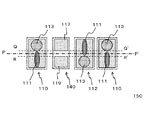
図1は、本実施形態の半導体装置の構成を示す平面図である。図1中のP−P’は、矩形のボンディングパッド110の長辺の中心線であり、Q−Q’は、プロービング傷111形成領域とボンディング領域113との境界線である。また、図2は、図1のA−A’断面図である。
図1に示した半導体装置100は、一つのパッド中にボンディング領域113と試験用プローブ接触領域(プロービング傷111形成領域)とを含むボンディングパッド110と、ボンディングパッド110から離隔して設けられて、ボンディング領域113とプロービング傷111形成領域との境界(Q−Q’)を示すように構成されたエリア識別マーク(打ち分けマーク120)と、を有する。打ち分けマーク120は、半導体装置100の素子形成面において、目視等により識別可能な領域である。
半導体装置100は、打ち分けマーク120の占める領域の輪郭に基づいて、境界を検知することができるように構成されている。たとえば、半導体装置100において、打ち分けマーク120の輪郭上の所定の位置における接線の延長線上に境界が位置する構成とすることができる。また、輪郭の少なくとも一部が直線状である場合、直線部分の延長線上に境界が位置する構成とすることができる。
図1においては、打ち分けマーク120は、略矩形の平面形状を有し、矩形の一辺が、境界を示す。さらに具体的には、矩形の一辺の延長線上に境界が位置する。なお、本明細書において、略矩形の平面形状は、少なくとも矩形の一辺が境界を示す直線領域を有する構成であればよく、たとえば矩形の角部が製造プロセス中で除去されて、丸みを帯びた形状になっていてもよい。また、打ち分けマーク120の平面形状は、矩形には限られず、台形であってもよい。さらに、打ち分けマーク120の平面形状が、三角形等の多角形の形状であってもよい。
また、打ち分けマーク120の占める領域の幅が、ボンディング領域113の幅またはプロービング傷111形成領域の幅を示す。ここで、領域の幅は、所定の方向における領域の端部間の長さのことである。たとえば、打ち分けマーク120が矩形の平面形状を有する場合、矩形の対向する辺の間隔を領域の幅とすることができる。このとき、ボンディングパッド110において、当該対向する辺を延長した延長線の間隔が、ボンディング領域113の幅またはプロービング傷111形成領域の幅となる。図1では、打ち分けマーク120の占める領域の幅が、プロービング傷111形成領域の幅となっている。
半導体装置100は、複数のボンディングパッド110を有し、一つの打ち分けマーク120が、複数のボンディングパッド110のそれぞれについて、境界を示すように構成されている。さらに具体的には、半導体装置100は、複数の打ち分けマーク120が直線状に配置された列を有し、一つの列あたり少なくとも一つの打ち分けマーク120が設けられるとともに、一つの打ち分けマーク120が、一つの列を構成するボンディングパッド110の前記境界を示す。図1では、列中のすべてのボンディングパッド110の境界が、一つの打ち分けマーク120によって示されている。
また、打ち分けマーク120の輪郭の少なくとも一部が直線状であって、この直線部分が、列の延在方向に平行に配置され、直線部分の延長線上に、一つの列を構成するボンディングパッド110の境界が位置する。
ボンディングパッド110と打ち分けマーク120とは、同一水準に形成されるとともに、同一材料により構成される。また、ボンディングパッド110および打ち分けマーク120は、素子形成面から金属等の導電性材料が露出されてなる領域である。
半導体装置100は、半導体基板(シリコン基板101)と、シリコン基板101の上部に設けられるとともに、所定の領域に開口部が設けられた有機樹脂からなる保護膜(ポリイミド膜105)と、をさらに有し、開口部の輪郭が打ち分けマーク120の輪郭を構成している。有機樹脂は、たとえばポリイミド、またはポリパラフェニレンベンズオキサゾール(PBO)である。図1および図2においては、有機樹脂をポリイミドでとした例を示しているが、有機樹脂をPBOとしてもよく、この場合、ポリイミド膜105に代えてPBO膜を設けることができる。
(First embodiment)
FIG. 1 is a plan view showing the configuration of the semiconductor device of this embodiment. In FIG. 1, PP ′ is a center line of the long side of the
The
The
In FIG. 1, the
Further, the width of the region occupied by the
The
In addition, at least a part of the outline of the
The
The
以下、半導体装置100の構成をさらに詳細に説明する。
半導体装置100は、シリコン基板101(図2)と、シリコン基板101上に設けられた多層膜103(図2)と、多層膜103上に設けられたボンディングパッド110および打ち分けマーク120とを有する。ボンディングパッド110および打ち分けマーク120は、Al膜等の金属膜とその上部に設けられたポリイミド膜105の開口部により構成される。Al膜形成領域108の周縁およびその近傍をポリイミド膜105が被覆しており、ポリイミド膜105に被覆されていない領域がAl膜露出部107となっている。また、ボンディングパッド110および打ち分けマーク120は、同一材料により、同一水準、具体的には同層に形成される。さらに、これらは同一工程で形成可能である。また、ボンディングパッド110および打ち分けマーク120は、それぞれ、多層膜103上の所定の位置に所定の数だけ配置される。
Hereinafter, the configuration of the
The
ポリイミド膜105は、パッシベーション膜として機能し、多層膜103の上面を被覆している。また、ポリイミド膜105には、ボンディングパッド110および打ち分けマーク120の形成領域に開口部が設けられており、開口部から、ボンディングパッド110および打ち分けマーク120の表面が露出している。
The
平面視において、ポリイミド膜105の開口部の輪郭は、ボンディングパッド110および打ち分けマーク120の輪郭を構成している。ボンディングパッド110および打ち分けマーク120の平面形状は、それぞれ矩形である。図1では、特に、打ち分けマーク120の平面形状が正方形である構成が例示されている。また、一つのボンディングパッド110には、プロービング傷111の形成領域であるプローブ接触領域と、ボンディングがなされるボンディング領域113とが設けられている。打ち分けマーク120は、ボンディングパッド110の形成領域以外の領域にボンディングパッド110から離隔して設置されており、プロービング傷111とボンディング領域113とのエリア分けを行う。
In plan view, the contour of the opening of the
打ち分けマーク120の寸法は、たとえば矩形の一辺の長さを15μm以上、好ましくは20μm以上とすることができる。こうすることにより、打ち分けマーク120の製造安定性をさらに向上させることができるとともに視認性も向上する。また、打ち分けマーク120の一辺の長さの上限に特に制限はないが、大きすぎると打ち分けマーク120の占める領域の面積が大きくなりすぎる。この点をさらに考慮すると、たとえば矩形の短辺の長さを20μm以上40μm以下とすることができる。また、長辺の長さはパッドの大きさに応じ、設定することができる。
As for the size of the
半導体装置100は、複数のボンディングパッド110を有する。複数のボンディングパッド110は、シリコン基板101の周縁の近傍の領域に、矩形の長辺の中心が同一直線上(図1中のP−P’)に位置するように、シリコン基板101の周縁に沿って一列に配置されている。また、プロービング傷111形成領域とボンディング領域113との境界線(Q−Q’)についても、一つの列中に配置された複数のボンディングパッド110について、同一直線上に配置されている。
The
なお、図1では、ボンディングパッド110において、ボンディング領域113の幅(P−P’に垂直な方向の長さ)よりもプロービング傷111形成領域の幅の方が大きい構成を例示したが、ボンディング領域113とプロービング傷111形成領域との面積の大小関係に特に制限はない。
1 illustrates a configuration in which the width of the probing
次に、半導体装置100の製造方法を説明する。
半導体装置100は、図1および図2に示した半導体装置を準備する工程と、打ち分けマーク120により境界(Q−Q’)を検知し、検知された境界に基づきプロービング傷111形成領域に試験用プローブを接触させる工程と、試験用プローブを接触させる工程の後、検知された境界に基づきボンディング領域113に外部接続用導体を接合させる工程と、を含む。外部接続用導体は、たとえばワイヤボンディング接続に用いられる導体とする。
Next, a method for manufacturing the
The
さらに具体的には、半導体装置100は、たとえば以下の手順により、既に知られた方法を用いて製造することができる。まず、シリコン基板101上に、配線層および層間絶縁膜等が積層した多層膜103を形成する。そして、最上層の層間絶縁膜上にAl膜を形成する。つづいて、Al膜を、ボンディングパッド110と打ち分けマーク120の形状にパターニングする。Al膜の形状は、ボンディングパッド110および打ち分けマーク120の周縁から所定量外側に張り出した形状とする。
More specifically, the
次に、パターニングされたAl膜の上面全面にポリイミド膜105を塗布法により形成する。そして、ボンディングパッド110および打ち分けマーク120の形状に対応する平面形状を有するマスクパターンをポリイミド膜105上に設ける。マスクを用いて、ボンディングパッド110および打ち分けマーク120の形成領域を選択的に除去してポリイミド膜105に開口部を形成し、開口部からAl膜を露出させ、Al膜形成領域108の一部をAl膜露出部107とする。以上の手順により、ボンディングパッド110および打ち分けマーク120が設けられた半導体装置が得られる。
Next, a
その後、ボンディングパッド110のプローブ接触領域にプローブを接触させて、針跡確認を行う。このとき、打ち分けマーク120を使用してプローブのプロービング傷111形成領域を設定する。具体的には、打ち分けマーク120の外周縁、ここでは矩形の一辺の延長(図1におけるQ−Q’)が、プローブ接触領域の端部、すなわちプロービング傷111形成領域とボンディング領域113との境界に対応する。そこで、この端部よりも内側にプローブを接触させてボンディングパッド110上を滑らせる。このとき、プロービング傷111形成領域内において、Al膜露出部107の表面にプロービング傷111が形成される。以上の手順により、図1に示した半導体装置100が得られる。
Thereafter, the probe is brought into contact with the probe contact area of the
また、その後、プロービング後の針跡を確認する際に、打ち分けマーク120を用いて良品判定を行う。具体的には、図1における境界Q−Q’よりも打ち分けマーク120から遠ざかる側にプロービング傷111が形成されているかどうかにより判定を行う。そして、良品については、ボンディングパッド110のボンディング領域113に、外部接続用の導電部材を接合する。このときにも、打ち分けマーク120を用いてプロービング傷111形成領域とボンディング領域113との境界を検知して、検知された境界よりも内側にボンディングを行う。具体的には、ボンディング領域113にボンディングワイヤをボンディングする。また、ボンディングワイヤ先端を溶解させてボール状とし、このボールをボンディング領域113に接合した後、ワイヤを引き抜いて除去することにより、バンプを形成してもよい。外部接続用の導電部材の材料は、たとえば、Al、AuまたはCu等の金属とする。
In addition, after that, when confirming the needle trace after probing, the non-defective product is determined using the hitting
次に、半導体装置100(図1、図2)の効果を説明する。
図1および図2に示した半導体装置100においては、打ち分けマーク120がボンディングパッド110から離隔して設けられている。このため、ボンディングパッド110を設置する際の空きスペースを利用してボンディングパッド110を配置することができる。
Next, effects of the semiconductor device 100 (FIGS. 1 and 2) will be described.
In the
また、ボンディングパッド110はポリイミド膜105とその開口部から露出しているAl膜とから構成され、打ち分けマーク120形成領域の輪郭がポリイミド膜105の開口部の輪郭となっている。このため、プロービング傷111形成領域とボンディング領域113との境界の視認性に優れた構成となっている。よって、プロービング傷111を所定の領域内に確実に形成し、ボンディング領域113の側にはみ出すことを抑制できる。したがって、ボンディング領域113におけるプロービング傷111とボンディングとの重なりにより生じるボンディングの剥離を抑制することができる。このため、ボンディング時の不良の発生を抑制し、製造歩留まりに優れた構成となっている。
The
また、半導体装置100では、打ち分けマーク120の端部をなす矩形の一辺がプロービング傷111形成領域とボンディング領域113との境界を示し、矩形の一辺の延長線上に境界が位置する構成となっている。このため、境界の位置をさらに確実に検知できる構成となっている。そして、打ち分けマーク120の幅が、プロービング傷111形成領域の幅に対応している。このため、プロービングを行う際にボンディングパッド110中のどちら側の領域がプロービング傷111形成領域であるかを容易に識別可能な構成であるとともに、その境界の視認性に優れた構成となっている。境界に加えて領域幅が示される構成となるため、プローブの接触またはボンディングを、所定の領域内でさらに確実に行うことができる。
Further, in the
また、半導体装置100においては、ボンディングの際には、打ち分けマーク120の非形成領域の側にボンディングを行えばよく、上述したように境界の視認性に優れるため、ボンディングの過程においても、作業者が目視によりボンディング領域113の境界内に確実に導電部材を接合することができる。
Further, in the
半導体装置100は、プローバでのプロービングエリア設定時に、打ち分けマーク120により境界およびプロービング傷111形成領域の幅を検知して設定を行うとともに、プロービング後の針跡確認時にも、打ち分けマーク120を基準として良品判定を行う。そして、ボンディング時においても、打ち分けマーク120を基準として境界を検知する。このため、プロービングおよびボンディングを行う位置をそれぞれ確実に検知し、境界内の所定の領域に確実に行うことができる。そして、所定のプロービング傷111形成領域にプロービングされているかどうかの確認が容易となり、作業者によるプロービング位置の良不良判定を容易に行うことができる。このため、チップ不良の予防管理を目視により確実に行うことが可能であるとともに、半導体装置100製造時のウェーハ検査工程における外観不良の判定を目視により容易にできる構成となっている。
When the probing area is set by the prober, the
また、背景技術の項で述べた特許文献1〜特許文献4に記載の装置においては、ボンディングパッド中に突起部等としてマークが設けられているため、一つのボンディングパッドに対して、一つ(一対)のマークを設ける必要があった。また、一つのマークからは一つのボンディングパッドにおける境界位置の情報しか得られず、ボンディングパッドすべてに突起部を設ける必要があった。さらに、前述したように、実際に突起部を形成しようとしても、ボンディング領域とプローブ領域との境界を認識するのに充分な微細加工が困難となる懸念があった。たとえば、本発明者の検討によれば、ポリイミド膜105の厚さを5μm〜6μm程度とした場合、ポリイミド膜105の幅が13μmよりも細い場合には、ポリイミド膜105が転倒する懸念があった。
Further, in the apparatus described in Patent Document 1 to Patent Document 4 described in the background art section, since a mark is provided as a protrusion or the like in the bonding pad, one ( It was necessary to provide a pair of marks. Further, only information on the boundary position in one bonding pad can be obtained from one mark, and it is necessary to provide a protrusion on all the bonding pads. Further, as described above, there is a concern that fine processing sufficient to recognize the boundary between the bonding region and the probe region may be difficult even if the projection is actually formed. For example, according to the study of the present inventor, when the thickness of the
これに対し、半導体装置100では、ボンディングパッド110から離隔して打ち分けマーク120を設けるとともに、打ち分けマーク120を所定の面積を占める領域としているため、上記特許文献1〜特許文献4で必要な微細加工が不要となり、打ち分けマーク120が確実に製造可能な構成であるとともに、製造安定性に優れた構成となっている。また、ボンディングパッド110から離隔して打ち分けマーク120を設けることにより、ボンディングパッド110および打ち分けマーク120のそれぞれを所定の位置に所定の個数配置することが可能である。また、平面構成の自由度を向上させることができる。また、半導体装置100は、複数のボンディングパッド110を有し、一つの打ち分けマーク120が、複数のボンディングパッド110のそれぞれについて、境界を示すように構成されている。このように、複数のボンディングパッド110につき打ち分けマーク120を一つとすれば、装置構成全体を簡素化することができる。
On the other hand, the
さらに、半導体装置100では、ボンディングパッド110と打ち分けマーク120とが、同一水準に形成されるとともに、同一材料により構成されるため、ボンディングパッド110と打ち分けマーク120とを同一工程で作製することができる。よって、製造プロセスを簡素化することができる。
Furthermore, in the
なお、図1では、3つのボンディングパッド110が一直線状に配置され、隣り合う二つのボンディングパッド110の間に一つの打ち分けマーク120が設けられている構成を例示したが、ボンディングパッド110および打ち分けマーク120の数および配置は、打ち分けマーク120の輪郭すなわち外周縁が、列中のボンディングパッド110のプロービング傷111の形成領域またはボンディング領域113の端部の位置を示すように配置されていればよく、図示した配置には限られない。
1 illustrates a configuration in which three
図3および図4は、ボンディングパッド110および打ち分けマーク120の平面配置の他の例を模式的に示す図である。
3 and 4 are diagrams schematically showing another example of the planar arrangement of the
図3においては、複数のボンディングパッド110が、スクライブ中心115の近傍の所定の位置に一直線状に配置されている。そして、隣り合うボンディングパッド110間に充分な大きさの隙間がある箇所に、打ち分けマーク120が配置されている。このように、打ち分けマーク120をボンディングパッド110と離隔して設けることにより、ボンディングパッド110が配置されない空き領域に打ち分けマーク120を配置することができる。このため、シリコン基板101上のスペースを有効利用することができる。
In FIG. 3, a plurality of
また、図4には、一列のボンディングパッド110群の中で、両端に配置されたボンディングパッド110の外側に打ち分けマーク120を一つずつ配置した例が示されている。打ち分けマーク120は、一列のボンディングパッド110群に対して、ボンディングパッド110が設けられない領域に最低一つ設けることができるが、図4に示したように、一対の打ち分けマーク120を、ボンディングパッド110の列の両端に配置することもできる。こうすることにより、一つの打ち分けマーク120の側からプローバを走査し、他方の打ち分けマーク120に至った際に、プローバ走査時の位置ずれの有無を確認することができる。そして、位置ずれが生じていた場合には、打ち分けマーク120を用いてプローバ位置の修正を行うことができる。よって、プローバの位置合わせ精度をより一層向上させることができる。
FIG. 4 shows an example in which one of the marking marks 120 is arranged outside the
また、半導体装置100においては、プロービング傷111の形成領域の形状に対応した平面形状を有するボンディングパッド110を用い、これを、隣り合う二つのプロービング傷111の形成領域間に配置して、プロービング傷111形成領域の幅を示す構成を例示したが、ボンディングパッド110がボンディング領域113の幅を示す構成としてもよい。
Further, in the
図5は、このような半導体装置の構成を示す平面図である。なお、図5および図6〜図9に示す半導体装置においては、シリコン基板101および多層膜103を不図示とする。
FIG. 5 is a plan view showing the configuration of such a semiconductor device. 5 and FIGS. 6 to 9, the
図5に示した半導体装置130は、図1に示した打ち分けマーク120に代えて、打ち分けマーク122を有する。打ち分けマーク122の基本構成は図1に示した打ち分けマーク120と同様であるが、ボンディング領域113の平面形状に対応する平面形状を有する点が異なる。また、図5においては、隣り合う二つのボンディング領域113の間に打ち分けマーク122が配置され、打ち分けマーク122の外周縁のうち、矩形の一辺がボンディング領域113の端部(図5中のQ−Q’)を示し、打ち分けマーク122の幅がボンディング領域113の幅を示している。図5の半導体装置130においても、図1の半導体装置100と同様の効果が得られる。
A
以下の実施形態においては、第一の実施形態と異なる点を中心に説明する。 In the following embodiment, it demonstrates centering on a different point from 1st embodiment.
(第二の実施形態)
第一の実施形態の半導体装置(図1〜図5)においては、一つの打ち分けマークが、一列のボンディングパッド110群の一つの境界の目印となる場合を説明したが、一つの打ち分けマークが、複数の境界を示す構成とすることができる。
(Second embodiment)
In the semiconductor device according to the first embodiment (FIGS. 1 to 5), the case where one marking mark serves as a mark of one boundary of a group of
図6は、本実施形態の半導体装置の構成を示す平面図である。
図6に示した半導体装置150は、ボンディングパッドの列の延在方向に沿って、ボンディング領域113とプロービング傷111形成領域とが交互に配置されるとともに、一つの打ち分けマーク140が、列を構成する一のボンディングパッド110の境界(Q−Q’)と、一のボンディングパッドに隣接する他のボンディングパッド112の境界(R−R’)とを示すように構成されている。
FIG. 6 is a plan view showing the configuration of the semiconductor device of this embodiment.
In the
図6に示した半導体装置150においては、ボンディングパッド110およびボンディングパッド112が同一直線上(P−P’)に交互に配置された構成となっている。ボンディングパッド110とボンディングパッド112とは同じ平面形状を有するが、ボンディングパッド112は、中心線P−P’に対してプロービング傷111の形成領域とボンディング領域113の形成領域とがボンディングパッド110と反対側に配置されている。つまり、ボンディング領域113が中心線P−P’に対して千鳥状に配置されている。
The
このような構成においては、打ち分けマーク140は、ボンディングパッド110におけるプロービング傷111形成領域とボンディング領域113との境界に加えて、ボンディングパッド112におけるプロービング傷111形成領域とボンディング領域113の境界も示す構成とする必要がある。従来のマークではこのような構成となっていなかったため、千鳥状にプロービングを行おうとすると、ボンディングパッド110またはボンディングパッド112のいずれかにおいてプロービング傷111がボンディング領域113の側に侵出してしまう懸念があった。
In such a configuration, the
そこで、半導体装置150においては、一つの打ち分けマーク140中に、第一のAl膜露出部117と第二のAl膜露出部119とが設けられた構成が採用されている。第一のAl膜露出部117および第二のAl膜露出部119の平面形状はともに矩形であり、それぞれ、図1に示した半導体装置100中の打ち分けマーク120のAl膜露出部107と同じ形状となっている。
Therefore, the
このように、二つのAl膜露出部を中心線P−P’の両側に一つずつ配置した平面形状の打ち分けマーク140を設けることにより、ボンディングパッド110におけるプロービング傷111形成領域とボンディング領域113との境界Q−Q’を第一のAl膜露出部117の一辺により認識可能となるのに加えて、さらに、ボンディングパッド110に隣接して設けられたボンディングパッド112におけるプロービング傷111形成領域とボンディング領域113との境界R−R’を第二のAl膜露出部119の一辺により認識することができる。このため、中心線P−P’に対して千鳥状にプロービングを行う際にも、プロービング傷111がボンディング領域113内に侵入することを抑制し、製造安定性を向上させることができる。また、打ち分けマーク140も、図1に示した打ち分けマーク120等と同様に、ボンディングパッド110およびボンディングパッド112から離隔して設けられているため、第一の実施形態と同様の効果が得られる。
In this way, by providing the planar marking marks 140 in which two exposed portions of the Al film are arranged on both sides of the center line PP ′, the probing
また、半導体装置150においては、一つの境界に対して一つのAl膜露出部が対応しているため、図7を参照して後述する構成に比べて、ポリイミド膜105の開口部の形成領域の大きさをさらに充分に確保することができる。このため、ポリイミド膜105への開口部の形成をより一層安定的に行うことが可能な構成となっている。
Further, in the
また、半導体装置150においては、打ち分けマーク140の形成領域の長さ(P−P’)方向の全体にわたって第一のAl膜露出部117と第二のAl膜露出部119とを設けることができるため、図8および図9を参照して後述する構成に比べて、プロービング傷111形成領域とボンディング領域113との境界をさらに検知しやすい構成となっている。
In the
図6においては、一つのボンディングパッド中に二つのAl膜の露出領域が設けられている構成について説明したが、一つのボンディングパッド中のAl膜の露出領域を一つとした場合にも、ボンディングパッド110の境界を複数示す構成とすることができる。図7および図9はこのような半導体装置の構成を示す平面図である。 In FIG. 6, the configuration in which two Al film exposed regions are provided in one bonding pad has been described. However, even when one Al film exposed region is included in one bonding pad, the bonding pad is also used. It can be set as the structure which shows multiple 110 boundaries. 7 and 9 are plan views showing the configuration of such a semiconductor device.
図7に示した半導体装置160では、打ち分けマーク124が矩形の平面形状を有し、境界Q−Q’上に打ち分けマーク124の一辺が配置されるとともに、境界R−R’上に他の一辺が配置されている。打ち分けマーク124の対向する二辺により境界Q−Q’と境界R−R’とが示され、これらが識別可能となるように構成されているため、図6に示した半導体装置150と同様の効果が得られる。また、半導体装置150に比べて打ち分けマーク124の構成をさらに簡素化することができる。
In the
また、図6では、中心線P−P’と垂直な直線上に第一のAl膜露出部117と第二のAl膜露出部119とが並んで配置された構成を例示したが、中心線P−P’と垂直な直線に対して第一のAl膜露出部117と第二のAl膜露出部119とを斜めに配置してもよい。
FIG. 6 illustrates the configuration in which the first Al film exposed
図8は、このようなボンディングパッドを有する半導体装置の構成を示す平面図である。図8に示した半導体装置170の基本構成は図6に示した半導体装置150と同様であるが、打ち分けマーク142において、第一のAl膜露出部117と第二のAl膜露出部119とが斜めに配置されている点が異なる。この構成では、第一のAl膜露出部117の端部と第二のAl膜露出部119の端部との間の最小距離が、図6に示した半導体装置150の打ち分けマーク140よりも大きくなっている。このため、ポリイミド膜105の開口部の形成をより一層安定的に行うことが可能である。
FIG. 8 is a plan view showing a configuration of a semiconductor device having such a bonding pad. The basic configuration of the
また、図7を参照して前述した一つの打ち分けマークを用いる構成の場合にも、境界Q−Q’を示す直線領域と境界R−R’を示す直線領域とを斜めに配置することができる。図9は、このような半導体装置の構成を示す平面図である。 Also in the case of the configuration using the single marking mark described above with reference to FIG. 7, the straight line region indicating the boundary QQ ′ and the straight line region indicating the boundary RR ′ may be arranged obliquely. it can. FIG. 9 is a plan view showing the configuration of such a semiconductor device.
図9に示した半導体装置180は、一つの打ち分けマーク126内に一つのAl膜露出部107が設けられ、Al膜露出部107の外周縁に階段状の段差が設けられた平面形状となっている。この階段部が、境界Q−Q’および境界R−R’を示す構成となっている。こうすることにより、図7に示した半導体装置160における打ち分けマーク124よりも、Al膜露出部107の面積をさらに充分に大きくすることができる。このため、ポリイミド膜105の開口部の形成時の製造安定性をさらに向上させることができる。
The
以上、図面を参照して本発明の実施形態について述べたが、これらは本発明の例示であり、上記以外の様々な構成を採用することもできる。 As mentioned above, although embodiment of this invention was described with reference to drawings, these are the illustrations of this invention, Various structures other than the above are also employable.
たとえば、以上の実施形態においては、ボンディングパッド110および打ち分けマーク上に設けられたパッシベーション膜がポリイミド膜105である場合を例に説明したが、パッシベーション膜を、ポリイミド膜等の有機絶縁膜に代えて、SiO2膜等の酸化膜や、SiN膜等の窒化膜としてもよい。また、パッシベーション膜は単層であってもよいし、複数の膜が積層されてなる積層膜であってもよい。以上の実施形態においては、ボンディングパッド110から離隔して打ち分けマークが設けられるため、これらのパッシベーション膜を用いる場合にも、製造安定性に優れた構成となっている。
For example, in the above embodiment, the case where the passivation film provided on the
また、打ち分けマークおよびボンディングパッド110を構成する導電膜は、Al膜には限られず、他に、たとえばAu膜やCu膜等の金属膜とすることもできる。
In addition, the conductive film constituting the mark and the
また、以上においては、Al膜形成領域108の一部をポリイミド膜105が被覆しており、ポリイミド膜105の開口部の輪郭が打ち分けマークの輪郭である場合を例に説明したが、Al膜形成領域108の全面が露出しており、Al膜形成領域108の輪郭が打ち分けマークの輪郭である構成としてもよい。
In the above description, the case where the Al
また、以上においては、打ち分けマークの平面形状が矩形である場合を中心に説明したが、打ち分けマークの形状は、矩形や図9に示した形状のように直線領域を有する形状には限られない。たとえば、図1に示した半導体装置100において、打ち分けマーク120の形状を、プロービング傷111の幅と同じ幅の楕円形とし、楕円の長径についての接線の延長線上にプロービング傷111形成領域とボンディング領域113との境界が位置するように構成してもよい。打ち分けマークの平面形状を、矩形や図9に示した形状のように直線領域を有する形状とすることにより、打ち分けマークの輪郭中の直線領域の延長線上に境界が位置するように配置することができるため、境界をより一層確実に検知可能な構成とすることができる。
In the above description, the case where the planar shape of the hitting mark is a rectangle has been mainly described. However, the shape of the hitting mark is limited to a rectangle or a shape having a linear region such as the shape shown in FIG. I can't. For example, in the
100 半導体装置
101 シリコン基板
103 多層膜
105 ポリイミド膜
107 Al膜露出部
108 Al膜形成領域
110 ボンディングパッド
111 プロービング傷
112 ボンディングパッド
113 ボンディング領域
115 スクライブ中心
117 第一のAl膜露出部
119 第二のAl膜露出部
120 打ち分けマーク
122 打ち分けマーク
124 打ち分けマーク
126 打ち分けマーク
130 半導体装置
140 打ち分けマーク
142 打ち分けマーク
150 半導体装置
160 半導体装置
170 半導体装置
180 半導体装置
DESCRIPTION OF
Claims (10)
前記ボンディングパッドから離隔して設けられて、前記ボンディング領域と前記試験用プローブ接触領域との境界を示すように構成されたエリア識別マークと、
を有し、
前記ボンディングパッドと、前記エリア識別マークとが、同一工程で同層に形成されるとともに、同一材料により構成されるとともに、
前記エリア識別マークの占める領域の輪郭に基づいて、前記境界を検知することができるように構成されたことを特徴とする半導体装置。 A bonding pad including a bonding area and a test probe contact area in one pad;
An area identification mark provided apart from the bonding pad and configured to indicate a boundary between the bonding region and the test probe contact region;
Have
The bonding pad and the area identification mark are formed in the same layer in the same process and are made of the same material,
A semiconductor device configured to be able to detect the boundary based on an outline of a region occupied by the area identification mark.
前記エリア識別マークが、略矩形の平面形状を有し、
前記矩形の一辺が、前記境界を示すことを特徴とする半導体装置。 The semiconductor device according to claim 1,
The area identification mark has a substantially rectangular planar shape,
One side of the rectangle indicates the boundary.
前記エリア識別マークの占める領域の幅が、前記ボンディング領域の幅または前記試験用プローブ接触領域の幅を示すことを特徴とする半導体装置。 The semiconductor device according to claim 1 or 2,
The width of the area occupied by the area identification mark indicates the width of the bonding area or the width of the test probe contact area.
複数の前記ボンディングパッドを有し、
一つの前記エリア識別マークが、複数の前記ボンディングパッドのそれぞれについて、前記境界を示すように構成されたことを特徴とする半導体装置。 The semiconductor device according to any one of claims 1 to 3,
A plurality of the bonding pads;
A semiconductor device, wherein one area identification mark is configured to indicate the boundary for each of a plurality of the bonding pads.
複数の前記ボンディングパッドが直線状に配置された列を有し、
一つの前記列あたり少なくとも一つの前記エリア識別マークが設けられるとともに、一つの前記エリア識別マークが、一つの前記列を構成する前記ボンディングパッドの前記境界を示すことを特徴とする半導体装置。 The semiconductor device according to claim 4,
A plurality of the bonding pads have a row arranged in a straight line,
At least one area identification mark is provided per one row, and one area identification mark indicates the boundary of the bonding pad constituting one row.
前記列の延在方向に沿って、前記ボンディング領域と前記試験用プローブ接触領域とが交互に配置されるとともに、
一つの前記エリア識別マークが、前記列を構成する一の前記ボンディングパッドの前記境界と、前記一のボンディングパッドに隣接する他のボンディングパッドの前記境界とを示すように構成されたことを特徴とする半導体装置。 The semiconductor device according to claim 5,
The bonding regions and the test probe contact regions are alternately arranged along the extending direction of the rows,
One of the area identification marks is configured to indicate the boundary of one bonding pad constituting the row and the boundary of another bonding pad adjacent to the one bonding pad. Semiconductor device.
半導体基板と、
前記半導体基板の上部に設けられるとともに、所定の領域に開口部が設けられた有機樹脂からなる保護膜と、
をさらに有し、
前記開口部の輪郭が前記エリア識別マークの輪郭を構成していることを特徴とする半導体装置。 The semiconductor device according to claim 1,
A semiconductor substrate;
A protective film made of an organic resin provided on the semiconductor substrate and having an opening in a predetermined region;
Further comprising
The semiconductor device, wherein an outline of the opening constitutes an outline of the area identification mark.
前記エリア識別マークにより前記境界を検知し、検知された前記境界に基づき前記試験用プローブ接触領域に試験用プローブを接触させる工程と、
試験用プローブを接触させる前記工程の後、検知された前記境界に基づき前記ボンディング領域に外部接続用導体を接合させる工程と、
を含むことを特徴とする半導体装置の製造方法。 Preparing the semiconductor device according to any one of claims 1 to 9,
Detecting the boundary by the area identification mark, and bringing the test probe into contact with the test probe contact area based on the detected boundary;
After the step of contacting the test probe, joining the external connection conductor to the bonding region based on the detected boundary;
A method for manufacturing a semiconductor device, comprising:
Priority Applications (3)
| Application Number | Priority Date | Filing Date | Title |
|---|---|---|---|
| JP2005031999A JP4585327B2 (en) | 2005-02-08 | 2005-02-08 | Semiconductor device and manufacturing method thereof |
| US11/342,527 US7294930B2 (en) | 2005-02-08 | 2006-01-31 | Semiconductor device and manufacturing process therefor |
| CNB2006100064634A CN100426497C (en) | 2005-02-08 | 2006-02-08 | Semiconductor device and manufacturing process therefor |
Applications Claiming Priority (1)
| Application Number | Priority Date | Filing Date | Title |
|---|---|---|---|
| JP2005031999A JP4585327B2 (en) | 2005-02-08 | 2005-02-08 | Semiconductor device and manufacturing method thereof |
Publications (3)
| Publication Number | Publication Date |
|---|---|
| JP2006222147A JP2006222147A (en) | 2006-08-24 |
| JP2006222147A5 JP2006222147A5 (en) | 2007-12-27 |
| JP4585327B2 true JP4585327B2 (en) | 2010-11-24 |
Family
ID=36911737
Family Applications (1)
| Application Number | Title | Priority Date | Filing Date |
|---|---|---|---|
| JP2005031999A Active JP4585327B2 (en) | 2005-02-08 | 2005-02-08 | Semiconductor device and manufacturing method thereof |
Country Status (3)
| Country | Link |
|---|---|
| US (1) | US7294930B2 (en) |
| JP (1) | JP4585327B2 (en) |
| CN (1) | CN100426497C (en) |
Families Citing this family (12)
| Publication number | Priority date | Publication date | Assignee | Title |
|---|---|---|---|---|
| JP5148825B2 (en) * | 2005-10-14 | 2013-02-20 | ルネサスエレクトロニクス株式会社 | Semiconductor device and manufacturing method of semiconductor device |
| JP4930322B2 (en) * | 2006-11-10 | 2012-05-16 | ソニー株式会社 | Semiconductor light emitting device, optical pickup device, and information recording / reproducing device |
| JP5027605B2 (en) * | 2007-09-25 | 2012-09-19 | パナソニック株式会社 | Semiconductor device |
| JP5323406B2 (en) * | 2008-06-24 | 2013-10-23 | ルネサスエレクトロニクス株式会社 | Manufacturing method of semiconductor integrated circuit device |
| JP5160498B2 (en) * | 2009-05-20 | 2013-03-13 | ルネサスエレクトロニクス株式会社 | Semiconductor device |
| JP5318055B2 (en) | 2010-09-22 | 2013-10-16 | 株式会社東芝 | Semiconductor device and manufacturing method of semiconductor device |
| DE102011004106A1 (en) * | 2010-12-28 | 2012-06-28 | Robert Bosch Gmbh | Printed circuit board, method for producing a printed circuit board and test device for testing a printed circuit board |
| JP6348009B2 (en) * | 2014-07-15 | 2018-06-27 | ラピスセミコンダクタ株式会社 | Semiconductor device |
| CN106783802A (en) * | 2016-11-22 | 2017-05-31 | 上海华力微电子有限公司 | Particular electrical circuit test miniature gasket construction and preparation method thereof in a kind of chip |
| JP2021150307A (en) * | 2020-03-16 | 2021-09-27 | ソニーセミコンダクタソリューションズ株式会社 | Semiconductor device, manufacturing method of the semiconductor device, and electronic apparatus |
| US20220359456A1 (en) * | 2021-05-10 | 2022-11-10 | Ap Memory Technology Corporation | Semiconductor structure and methods for bonding tested wafers and testing pre-bonded wafers |
| CN117199054A (en) * | 2022-06-01 | 2023-12-08 | 长鑫存储技术有限公司 | Packaging structure, manufacturing method thereof and semiconductor device |
Citations (4)
| Publication number | Priority date | Publication date | Assignee | Title |
|---|---|---|---|---|
| JP2001177066A (en) * | 1999-09-16 | 2001-06-29 | Samsung Electronics Co Ltd | Integrated circuit device |
| JP2001176876A (en) * | 1999-12-17 | 2001-06-29 | Matsushita Electronics Industry Corp | High breakdown voltage semiconductor device |
| JP2001338955A (en) * | 2000-05-29 | 2001-12-07 | Texas Instr Japan Ltd | Semiconductor device and its manufacturing method |
| JP2006210631A (en) * | 2005-01-28 | 2006-08-10 | Nec Electronics Corp | Semiconductor device |
Family Cites Families (10)
| Publication number | Priority date | Publication date | Assignee | Title |
|---|---|---|---|---|
| JPH01129432A (en) * | 1987-11-16 | 1989-05-22 | Nec Corp | Integrated circuit |
| JPH04215450A (en) * | 1990-12-14 | 1992-08-06 | Mitsubishi Electric Corp | Semiconductor integrated circuit device |
| JPH08115958A (en) * | 1994-08-24 | 1996-05-07 | Nec Corp | Semiconductor device |
| JPH09213757A (en) * | 1996-02-07 | 1997-08-15 | Kawasaki Steel Corp | Method for facilitating wafer probe |
| JP3843624B2 (en) * | 1998-11-27 | 2006-11-08 | 松下電器産業株式会社 | Semiconductor integrated circuit device and method for assembling semiconductor integrated circuit device |
| US6563226B2 (en) * | 2001-05-23 | 2003-05-13 | Motorola, Inc. | Bonding pad |
| US6844631B2 (en) * | 2002-03-13 | 2005-01-18 | Freescale Semiconductor, Inc. | Semiconductor device having a bond pad and method therefor |
| US6784556B2 (en) | 2002-04-19 | 2004-08-31 | Kulicke & Soffa Investments, Inc. | Design of interconnection pads with separated probing and wire bonding regions |
| JP3724464B2 (en) * | 2002-08-19 | 2005-12-07 | 株式会社デンソー | Semiconductor pressure sensor |
| US6765228B2 (en) | 2002-10-11 | 2004-07-20 | Taiwan Semiconductor Maunfacturing Co., Ltd. | Bonding pad with separate bonding and probing areas |
-
2005
- 2005-02-08 JP JP2005031999A patent/JP4585327B2/en active Active
-
2006
- 2006-01-31 US US11/342,527 patent/US7294930B2/en active Active
- 2006-02-08 CN CNB2006100064634A patent/CN100426497C/en active Active
Patent Citations (4)
| Publication number | Priority date | Publication date | Assignee | Title |
|---|---|---|---|---|
| JP2001177066A (en) * | 1999-09-16 | 2001-06-29 | Samsung Electronics Co Ltd | Integrated circuit device |
| JP2001176876A (en) * | 1999-12-17 | 2001-06-29 | Matsushita Electronics Industry Corp | High breakdown voltage semiconductor device |
| JP2001338955A (en) * | 2000-05-29 | 2001-12-07 | Texas Instr Japan Ltd | Semiconductor device and its manufacturing method |
| JP2006210631A (en) * | 2005-01-28 | 2006-08-10 | Nec Electronics Corp | Semiconductor device |
Also Published As
| Publication number | Publication date |
|---|---|
| US7294930B2 (en) | 2007-11-13 |
| CN1819168A (en) | 2006-08-16 |
| CN100426497C (en) | 2008-10-15 |
| JP2006222147A (en) | 2006-08-24 |
| US20060186405A1 (en) | 2006-08-24 |
Similar Documents
| Publication | Publication Date | Title |
|---|---|---|
| JP4585327B2 (en) | Semiconductor device and manufacturing method thereof | |
| KR100721739B1 (en) | Semiconductor device, method and apparatus for testing same, and method for manufacturing semiconductor device | |
| US8508055B2 (en) | Semiconductor device and manufacturing method thereof | |
| JP4803966B2 (en) | Semiconductor device | |
| JP4372785B2 (en) | Manufacturing method of semiconductor integrated circuit device | |
| JP2006210631A (en) | Semiconductor device | |
| JP2006140276A (en) | Semiconductor wafer and semiconductor device using the same and chip size package, and semiconductor wafer manufacturing method and semiconductor wafer testing method | |
| JP4010244B2 (en) | Surface mount package | |
| KR101576955B1 (en) | Semiconductor device having bonding pad and semiconductor package having the same | |
| JP4746609B2 (en) | Semiconductor device and manufacturing method thereof | |
| TW531776B (en) | Metal pad structure suitable for connection pad and inspection pad | |
| JP5027605B2 (en) | Semiconductor device | |
| US8492763B2 (en) | Semiconductor device including an edge seal and plural pad pieces | |
| KR100727490B1 (en) | Semiconductor device with visible indicator for separating bonding region and probing region, and method of fabricating the same | |
| JP4914734B2 (en) | Semiconductor device | |
| TWI745829B (en) | Semiconductor device and detecting method of needle mark offset | |
| US20230163015A1 (en) | Semiconductor wafer and method for manufacturing semiconductor wafer | |
| US20100270672A1 (en) | Semiconductor device | |
| KR101126062B1 (en) | Semiconductor device and method of inspecting an electrical characteristic of a semiconductor device | |
| JP5300928B2 (en) | Semiconductor device | |
| JP2012033822A (en) | Semiconductor device and method of manufacturing the same | |
| KR20070015222A (en) | Process for fabricating semiconductor integrated circuit device | |
| JP2011171661A (en) | Semiconductor element and method of manufacturing semiconductor device |
Legal Events
| Date | Code | Title | Description |
|---|---|---|---|
| A521 | Request for written amendment filed |
Free format text: JAPANESE INTERMEDIATE CODE: A523 Effective date: 20071112 |
|
| A621 | Written request for application examination |
Free format text: JAPANESE INTERMEDIATE CODE: A621 Effective date: 20080117 |
|
| A977 | Report on retrieval |
Free format text: JAPANESE INTERMEDIATE CODE: A971007 Effective date: 20100205 |
|
| A131 | Notification of reasons for refusal |
Free format text: JAPANESE INTERMEDIATE CODE: A131 Effective date: 20100209 |
|
| A521 | Request for written amendment filed |
Free format text: JAPANESE INTERMEDIATE CODE: A523 Effective date: 20100412 |
|
| A131 | Notification of reasons for refusal |
Free format text: JAPANESE INTERMEDIATE CODE: A131 Effective date: 20100511 |
|
| A521 | Request for written amendment filed |
Free format text: JAPANESE INTERMEDIATE CODE: A523 Effective date: 20100712 |
|
| TRDD | Decision of grant or rejection written | ||
| A01 | Written decision to grant a patent or to grant a registration (utility model) |
Free format text: JAPANESE INTERMEDIATE CODE: A01 Effective date: 20100831 |
|
| A01 | Written decision to grant a patent or to grant a registration (utility model) |
Free format text: JAPANESE INTERMEDIATE CODE: A01 |
|
| A61 | First payment of annual fees (during grant procedure) |
Free format text: JAPANESE INTERMEDIATE CODE: A61 Effective date: 20100903 |
|
| R150 | Certificate of patent or registration of utility model |
Ref document number: 4585327 Country of ref document: JP Free format text: JAPANESE INTERMEDIATE CODE: R150 Free format text: JAPANESE INTERMEDIATE CODE: R150 |
|
| FPAY | Renewal fee payment (event date is renewal date of database) |
Free format text: PAYMENT UNTIL: 20130910 Year of fee payment: 3 |
|
| S531 | Written request for registration of change of domicile |
Free format text: JAPANESE INTERMEDIATE CODE: R313531 |
|
| R350 | Written notification of registration of transfer |
Free format text: JAPANESE INTERMEDIATE CODE: R350 |