JP4573763B2 - Adsorption device - Google Patents
Adsorption device Download PDFInfo
- Publication number
- JP4573763B2 JP4573763B2 JP2005348266A JP2005348266A JP4573763B2 JP 4573763 B2 JP4573763 B2 JP 4573763B2 JP 2005348266 A JP2005348266 A JP 2005348266A JP 2005348266 A JP2005348266 A JP 2005348266A JP 4573763 B2 JP4573763 B2 JP 4573763B2
- Authority
- JP
- Japan
- Prior art keywords
- suction
- semiconductor wafer
- holding layer
- pad
- hole
- Prior art date
- Legal status (The legal status is an assumption and is not a legal conclusion. Google has not performed a legal analysis and makes no representation as to the accuracy of the status listed.)
- Expired - Fee Related
Links
Images


Description
本発明は、半導体ウェーハのバックグラインド工程やダイシング工程等で使用される吸着装置に関するものである。 The present invention relates to a suction device used in a back grinding process or a dicing process of a semiconductor wafer.
半導体ウェーハは、半導体製造の前工程では反らないように厚いことが好ましいが、そのままの厚さでは薄化、小型化、軽量化が要求される近年の半導体パッケージには適さないので、バックグラインド工程と呼ばれる工程でグラインダ装置により裏面が削られ、薄くされた後、次工程に移される(特許文献1参照)。 The semiconductor wafer is preferably thick so that it does not warp in the pre-process of semiconductor manufacturing, but the thickness as it is is not suitable for recent semiconductor packages that require thinning, miniaturization, and weight reduction. After the back surface is cut and thinned by a grinder device in a process called a process, the process is transferred to the next process (see Patent Document 1).
半導体ウェーハをバックグラインド工程で薄くして次工程に移す場合には、先ず、750μm程度の厚さを有する半導体ウェーハWのパターン形成面に保護シート60を粘着して好ましい大きさにカット(図15参照)し、半導体ウェーハWをストッカーである基板収納カセット20Aに収納して図16に示すグラインダ装置61に搬送する。
When the semiconductor wafer is thinned in the back grinding process and transferred to the next process, first, the
基板収納カセット20Aをグラインダ装置61に搬送したら、このグラインダ装置61のチャックテーブル62に半導体ウェーハWをセットし、チャックテーブル62を回転させて半導体ウェーハWの裏面に粗研削と仕上げ研削とを回転砥石により順次施し、その後、バックグラインドにより50μm程度に薄化された半導体ウェーハWを基板収納カセット20Aに収納したり、洗浄装置63で洗浄する。
After the
そして、薄化された半導体ウェーハWをグラインダ装置61から下流にインラインされたストレスリリーフ装置64に搬送ラインで搬送し、半導体ウェーハWの強度が低下した裏面のダメージ層をエッチング液又はポリッシュにより除去して抗折強度を向上させた後、基板収納カセット20Aに半導体ウェーハWを収納すれば、薄化された半導体ウェーハWを基板収納カセット20Aにより次工程に移すことができる(特許文献2参照)。
従来における半導体ウェーハWは、以上のように薄化されて基板収納カセット20Aに単に収納されるが、非常に薄く(例えば、50μm以下の薄さ)、撓みやすく、割れやすいので、ハンドリング等の作業中に簡単に破損してしまうという大きな問題がある。また、弓なりに反ることが少なくないので、以後の作業でハンドリングすることができないという問題もある。
The conventional semiconductor wafer W is thinned as described above and simply stored in the
本発明は上記に鑑みなされたもので、例え基板が薄い場合でも、ハンドリング時等に容易に破損するのを抑制することのできる吸着装置を提供することを目的としている。 The present invention has been made in view of the above, and an object of the present invention is to provide an adsorption device that can suppress easy breakage during handling even when the substrate is thin.
本発明においては上記課題を解決するため、基板を保持する吸着治具を吸着パッドに取り外し可能に支持させた装置であって、
吸着治具は、剛性を有する板体と、この板体の表面に形成される凹部と、この凹部を被覆して基板を着脱自在に粘着保持する変形可能な保持層と、板体に設けられて保持層に被覆された凹部の気体を外部に排気する排気孔とを含み、凹部には、保持層を支持する複数の支持突起を設け、
吸着パッドは、吸着治具の板体裏面に重なるパッドと、このパッドから伸びるアームとを含み、パッドには、吸着治具の板体裏面に対向する対向穴と、吸着治具の排気孔に連通する連通穴とをそれぞれ設け、パッドとアームのうち少なくともアームには、パッドの対向穴に連通する給排路、及びパッドの連通穴に連通する排出路を設け、
吸着治具の凹部に保持層の一部を変形させて取り付け、この保持層の変形した一部から板体にかけて吸着パッドの対向穴に連通する貫通部を設けたことを特徴としている。
In the present invention, in order to solve the above-mentioned problem, an apparatus in which a suction jig for holding a substrate is removably supported on a suction pad ,
The suction jig is provided on the plate body having rigidity, a concave portion formed on the surface of the plate body, a deformable holding layer that covers the concave portion and detachably adheres and holds the substrate. An exhaust hole for exhausting the gas in the concave portion covered with the holding layer to the outside, and the concave portion is provided with a plurality of support protrusions for supporting the holding layer,
The suction pad includes a pad that overlaps the back surface of the suction jig plate and an arm that extends from the pad. The pad includes an opposing hole that faces the back surface of the suction jig and an exhaust hole of the suction jig. A communication hole that communicates with each other, and at least the arm of the pad and the arm is provided with a supply / discharge path that communicates with the opposing hole of the pad and a discharge path that communicates with the communication hole of the pad
It is characterized in that a part of the holding layer is deformed and attached to the concave portion of the suction jig, and a penetrating part communicating with the opposing hole of the suction pad is provided from the deformed part of the holding layer to the plate body .
なお、吸着パッドの給排路を給排装置に接続し、吸着パッドの排出路を負圧源に接続することができる。The suction pad supply / discharge path can be connected to a supply / discharge device, and the suction pad discharge path can be connected to a negative pressure source.
また、本発明においては上記課題を解決するため、基板収納カセットと、この基板収納カセットに収納可能に構成されるとともに、吸着パッドに支持され、基板を保持する吸着治具とを備えたものであって、
基板収納カセットは、複数の対向壁の間に架設(架け渡して設ける)される棚板と、この棚板に形成される凹部と、この凹部を被覆して基板あるいは吸着治具を着脱自在に粘着保持する可撓性の保持層と、この保持層に被覆された凹部内の気体を外部に排気する排気通路とを含んでなることを特徴としても良い。
In order to solve the above problems, the present invention comprises a substrate storage cassette and a suction jig configured to be stored in the substrate storage cassette, supported by a suction pad, and holding a substrate. There,
The substrate storage cassette has a shelf that is laid (bridged) between a plurality of opposing walls, a recess that is formed on the shelf, and a substrate or suction jig that can be attached to and detached from the recess. It may be characterized by comprising a flexible holding layer for holding adhesive and an exhaust passage for exhausting the gas in the recess covered by the holding layer to the outside.
なお、棚板の凹部に、保持層を支持する複数の突起を間隔をおいて並べ設けることができる。
また、排気通路を負圧源に取り外し可能に接続し、この負圧源を駆動して保持層を変形させることができる。
A plurality of protrusions that support the holding layer can be arranged in the recesses of the shelf plate at intervals.
Further, the exhaust passage can be detachably connected to the negative pressure source, and the negative pressure source can be driven to deform the holding layer.
さらに、本発明においては上記課題を解決するため、基板収納カセットと、この基板収納カセットに収納可能に構成されるとともに、吸着パッドに支持され、基板を保持する吸着治具とを備えたものであって、
基板収納カセットは、複数の対向壁の間に架設されて基板あるいは吸着治具を搭載する棚板と、この棚板に形成されて基板あるいは吸着治具に被覆される凹部と、負圧源の駆動に基づき、被覆された凹部内から外部に気体を排気する排気通路とを含み、凹部には、基板あるいは吸着治具を支持する複数の突起を設けたことを特徴としても良い。
Furthermore, in order to solve the above-described problems, the present invention includes a substrate storage cassette and a suction jig configured to be stored in the substrate storage cassette and supported by the suction pad and holding the substrate. There,
The substrate storage cassette is constructed between a plurality of opposing walls and mounted with a shelf plate on which a substrate or suction jig is mounted, a recess formed on the shelf plate and covered with the substrate or suction jig, and a negative pressure source. And an exhaust passage for exhausting gas from the covered recess to the outside based on the driving, and the recess may be provided with a plurality of protrusions for supporting the substrate or the suction jig.
ここで、特許請求の範囲における基板は、バックグラインドされた厚さ300μm以下の薄い半導体ウェーハ(例えば、口径200mmや300mmのシリコンウェーハ等)が主ではあるが、何らこれに限定されるものではない。例えば、厚い半導体ウェーハでも良いし、1mm以下の薄さが要求されるガラス基板、100μm以下の薄さが要望される可撓性の高密度フレキシブル配線板、液晶セル、あるいはプリント配線板等でも良い。 Here, the substrate in the claims is mainly a back-ground thin semiconductor wafer having a thickness of 300 μm or less (for example, a silicon wafer having a diameter of 200 mm or 300 mm), but is not limited thereto. . For example, it may be a thick semiconductor wafer, a glass substrate that requires a thickness of 1 mm or less, a flexible high-density flexible wiring board that requires a thickness of 100 μm or less, a liquid crystal cell, or a printed wiring board. .
吸着治具や吸着パッドのパッドは、基板と略同じ大きさ、基板よりも僅かに大きい大きさ、あるいは基板よりも僅かに小さい大きさに形成されることが好ましい。吸着治具の板体や凹部は、平面視で円形や多角形等に形成することができる。保持層は、単数のエラストマーからなるものでも良いし、性質(材料、硬度、弾性、粘度等)の異なる積層した複数のエラストマー等とすることもできる。 The suction jig or the pad of the suction pad is preferably formed to have substantially the same size as the substrate, slightly larger than the substrate, or slightly smaller than the substrate. The plate body and the concave portion of the suction jig can be formed in a circular shape or a polygonal shape in a plan view. The holding layer may be made of a single elastomer, or may be a plurality of laminated elastomers having different properties (material, hardness, elasticity, viscosity, etc.).
複数の支持突起は、凹部に規則的に配列されるものでも良いし、不規則に配列されるものでも良く、凹部と一体構造あるいは別体として設けることができる。各支持突起は、円錐台形、角柱形、角錐台形等に形成することができ、保持層に接着していても良いし、そうでなくても良い。 The plurality of support protrusions may be regularly arranged in the recesses, or may be irregularly arranged, and may be provided as an integral structure or separate from the recesses. Each support protrusion can be formed in a truncated cone shape, a prism shape, a truncated pyramid shape, or the like, and may or may not be adhered to the holding layer.
対向穴と連通穴とは、単数複数を特に問うものではなく、丸穴、楕円形の穴、円弧形の穴、矩形の穴、直線の複数の溝穴が一列に並んだり、X字形に配列された溝穴等でも良い。給排装置には、少なくとも負圧源の他、圧縮機やファン等が含まれる。さらに、負圧源は、例えば各種の真空ポンプや真空ブロワー等からなり、エジェクタ取り付けの有無を特に問うものではない。 The counter hole and the communication hole are not particularly limited to a single hole, but a round hole, an elliptical hole, an arc-shaped hole, a rectangular hole, and a plurality of straight grooves are arranged in a line, or in an X shape. An arrayed slot or the like may be used. The supply / discharge device includes at least a negative pressure source, a compressor, a fan, and the like. Further, the negative pressure source includes, for example, various vacuum pumps, vacuum blowers and the like, and does not particularly ask whether or not the ejector is attached.
本発明によれば、吸着装置により基板を保持する場合には、基板の被吸着面に吸着パッドに支持された吸着治具の保持層を重ねて接触させれば、保持層の粘着力により基板を略平らに保持することができる。
また、吸着治具の保持層から基板を取り外したい場合には、凹部内の気体を排気孔により凹部の外に排気すれば良い。すると、気体の排気に伴い、凹部の底方向に保持層が変形して基板との間に隙間を形成し、保持層と基板との接触部分が減少する。
According to the present invention, when the substrate is held by the suction device, if the holding layer of the suction jig supported by the suction pad is brought into contact with the suction surface of the substrate, the substrate is brought into contact with the adhesive force of the holding layer. Can be held substantially flat.
When it is desired to remove the substrate from the holding layer of the suction jig, the gas in the recess may be exhausted out of the recess through the exhaust hole. Then, as the gas is exhausted, the holding layer is deformed in the bottom direction of the recess to form a gap between the substrate and the contact portion between the holding layer and the substrate is reduced.
本発明によれば、例え半導体ウェーハ等の基板が薄い場合でも、ハンドリング時等に容易に破損することのないような吸着装置を提供することができるという効果がある。また、吸着装置の吸着治具を吸着パッドから取り外すことが可能なので、基板収納カセット、容器、あるいは治具等に基板、吸着治具、又は基板を搭載した吸着治具を適宜収納することができ、これにより、基板の搬送、ハンドリング、保管等の便宜を図ることができる。 According to the present invention, even if a substrate such as a semiconductor wafer is thin, it is possible to provide an adsorption device that is not easily damaged during handling or the like. In addition, since the suction jig of the suction device can be removed from the suction pad, the substrate, the suction jig, or the suction jig with the substrate mounted thereon can be appropriately stored in a substrate storage cassette, container, jig, or the like. This makes it possible to facilitate the transportation, handling, storage, etc. of the substrate.
また、吸着治具の凹部に保持層の一部を変形させて取り付け、この保持層の変形した一部から板体にかけて吸着パッドの対向穴に連通する貫通部を設けるので、基板と保持層の変形した一部との隙間に気体を給排して基板に対する保持力や解除力を高めることができ、これにより、基板の取り付け取り外しを容易にすることができる。 In addition, a part of the holding layer is deformed and attached to the concave portion of the suction jig, and a penetrating part communicating with the opposing hole of the suction pad is provided from the deformed part of the holding layer to the plate body. Gas can be supplied to and discharged from the gap between the deformed part and the holding force and the releasing force with respect to the substrate can be increased, thereby making it easy to attach and detach the substrate.
また、吸着パッドの給排路を給排装置に接続すれば、吸着治具を吸着パッドに真空吸着したり、取り外すことができる。さらに、吸着パッドの排出路を負圧源に接続すれば、凹部の気体を排気して保持層を変形させ、保持層に粘着した基板を取り外すことができる。 Moreover, if the suction pad supply / discharge path is connected to the supply / discharge device, the suction jig can be vacuum-sucked to or removed from the suction pad. Furthermore, if the suction path of the suction pad is connected to a negative pressure source, the gas in the recess can be exhausted to deform the holding layer, and the substrate adhered to the holding layer can be removed.
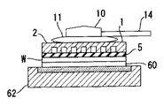
以下、図面を参照して本発明の好ましい実施の形態を説明すると、本実施形態における吸着装置は、図1ないし図16に示すように、バックグラインドにより薄化された半導体ウェーハW用の吸着治具1を吸着パッド10に取り外し可能に支持させ、この吸着パッド10により吸着治具1を、半導体製造装置であるグラインダ装置61から基板収納カセット20、洗浄装置63、あるいは次工程であるダイシング工程等に適宜搬送するようにしている。
Hereinafter, a preferred embodiment of the present invention will be described with reference to the drawings. As shown in FIGS. 1 to 16, the adsorption apparatus in this embodiment is an adsorption treatment for a semiconductor wafer W thinned by back grinding. The
半導体ウェーハWは、図1、図2、図6、図7、図10に示すように、例えば口径300mmのシリコンウェーハからなり、周縁部に結晶方向の判別や整列を容易にするノッチが平面略半楕円形に切り欠かれる。 As shown in FIGS. 1, 2, 6, 7, and 10, the semiconductor wafer W is made of, for example, a silicon wafer having a diameter of 300 mm, and the peripheral portion has a notch that makes it easy to determine and align the crystal direction. Cut out into a semi-elliptical shape.
吸着治具1は、図1や図2に示すように、剛性を有する薄い板体2と、この板体2に形成される凹み穴3と、この凹み穴3を被覆して半導体ウェーハWを着脱自在に粘着保持する弾性変形可能な保持層5と、この保持層5に被覆された凹み穴3の空気を排気する排気孔6とを備え、凹み穴3内には、保持層5を支持する複数の支持突起4が並設される。
As shown in FIGS. 1 and 2, the
板体2は、所定の材料を使用して半導体ウェーハWと略同じか、あるいは僅かに大きい円板形に形成され、半導体ウェーハWを粘着保持した状態、あるいは粘着保持しない状態で基板収納カセット20に水平に収納される。この板体2の材料としては、特に限定されるものではないが、例えば板体2に半導体ウェーハWが搭載された場合の撓み量を5mm以下に抑制可能なPC、PP、PE、アクリル樹脂、塩化ビニル樹脂、アルミニウム合金、マグネシウム合金、ガラス、ステンレス等があげられる。
The
凹み穴3は、図1ないし図5等に示すように、板体2の表面における周縁部を除く大部分に浅く凹み形成され、半導体ウェーハWよりも僅かに小さい円形に形成される。この凹み穴3の底面には、保持層5を接着支持する複数の支持突起4が隙間をおいて規則的に配列され、各支持突起4が凹み穴3の深さと略同じ長さ・高さの円柱形に形成される。複数の支持突起4は、例えば凹み穴3の底面に成形法、サンドブラスト法、エッチング法等により一体形成される。
As shown in FIG. 1 to FIG. 5 and the like, the recessed hole 3 is formed to be shallowly recessed at most of the surface of the
保持層5は、図1や図2に示すように、可撓性、粘着性、弾性の材料を使用して半導体ウェーハWと略同じか、あるいは僅かに大きい平面円形の柔軟な薄膜に成形され、板体2の表面周縁部に積層して接着されるとともに、各支持突起4の平坦な表面に接着されており、凹み穴3を被覆してその底面との間に空気流通用の空間を区画する。
As shown in FIGS. 1 and 2, the
保持層5の材料としては、特に限定されるものではないが、例えば耐熱性、耐候性、耐水性、剥離性、経時安定性等に優れるシリコーン系、ウレタン系、オレフィン系、フッ素系のエラストマーが使用される。この保持層5には、半導体ウェーハWの保護シート面側又は裏面側が選択的に保持される。
The material of the
排気孔6は、同図に示すように、板体2の外側厚さ方向に丸く穿孔され、保持層5に被覆された凹み穴3内の空気を排気するとともに、この空気の排気により平坦な保持層5を凹み穴3の底面方向に変形させ、保持層5と半導体ウェーハWとの界面に空気流入用の隙間を形成して粘着した半導体ウェーハWの剥離を容易化するよう機能する。
As shown in the figure, the
吸着パッド10は、同図に示すように、吸着治具1の裏面に接離可能に積層するパッド11と、このパッド11の後部から後方に直線的に伸びる長板形のアーム14とを備え、これらパッド11とアーム14とが所定の成形材料により透明に一体成形されており、アーム14が図示しないロボットに取付具を介しXYZ方向に移動可能、そして回転可能に支持される。
As shown in the figure, the
パッド11は、半導体ウェーハWや吸着治具1よりも僅かに小さい円板形に形成され、吸着治具1の板体裏面に重なる表面の中心部には、吸着治具1の板体裏面中心部に対向する拡径の対向溝穴12が浅く穿孔されており、表面の周縁部には、吸着治具1の排気孔6に重なって連通する連通溝穴13が深く穿孔される。
The
パッド11からアーム14の内部後方にかけては、パッド11の対向溝穴12に上流端部が連通する給排路15と、パッド11の連通溝穴13に上流端部が連通する排出路16とが互いに交差しないように並べて設けられ、アーム14の後部裏面から露出した給排路15の下流端部が真空ポンプからなる給排装置17に接続されており、アーム14の後部裏面から露出した排出路16の下流端部が真空ポンプからなる負圧源18に接続される。
From the
給排装置17は、対向溝穴12内の空気を排気してパッド11やその対向溝穴12に吸着治具1の裏面を真空吸着するよう機能する。また、負圧源18は、半導体ウェーハWの着脱に応じて駆動し、凹み穴3の空間の空気を排気孔6と連通溝穴13を介し外部に排気して保持層5を凹み穴3の底面方向に凹凸に変形させ、保持層5と半導体ウェーハWとの界面に空気流入用の隙間を形成して半導体ウェーハWの剥離を容易化する。
The supply /
基板収納カセット20は、フロントオープンボックスタイプのカセットケース21に内蔵して並べられる複数の棚板31と、各棚板31に形成される凹部である窪み穴32と、この窪み穴32を被覆して半導体ウェーハW又は吸着治具1を着脱自在に粘着保持する弾性変形可能な密着保持層34と、この密着保持層34に被覆された窪み穴32の空気を排気する複数の排気通路35とを備え、バックグラインド工程からその後の工程にかけて使用されるグラインダ装置61等からなる半導体製造装置やそのオープナ50に位置決め搭載される。
The
カセットケース21は、図6ないし図9に示すように、半導体ウェーハW又は吸着治具1の収納に十分な隙間をおいて相対向する左右一対の側壁22を備え、この一対の側壁22の下部間には底板23が水平に架設されるとともに、上端部間には天板24が水平に架設され、開口した背面には縦長の背面壁25が装着されており、正面が開口して薄化された半導体ウェーハWや吸着治具1の出し入れ口として機能する。
As shown in FIG. 6 to FIG. 9, the
カセットケース21の側壁22、底板23、天板24、及び背面壁25は、例えば耐衝撃性、耐熱性、耐水性等に優れる透明のPCやPEEK等の成形材料を使用して別々に成形され、ビスやナット等を介して組み立てられる。
The
カセットケース21の側壁22は上下方向に伸びる縦長の板に形成され、底板23の裏面における前部両側と後部中央とには、複数の位置決め具26が底面視で三角形を描くよう配設される。各位置決め具26は、平面略トラック形のブロックに形成され、オープナ50のステージから突出した位置決めピン51に摺接するV溝27が長手方向に切り欠かれており、このV溝27がオープナ50の位置決めピン51に上方から嵌合することにより、基板収納カセット20を高精度に位置決めするよう機能する。
The
カセットケース21の天板24には、RFIDシステムを構築するICタグ28が貼着されるとともに、把持用のハンドル29が着脱自在に装着され、背面壁25には、半導体ウェーハWや密着保持層34の視認を可能とする縦長の観察窓30が選択的に形成される。
An
複数の棚板31は、図6や図7に示すように、カセットケース21の内部上下方向に所定のピッチで配列され、棚板31と棚板31との間には、半導体ウェーハWや吸着治具1の出し入れに支障を来たさない空間が確保される。各棚板31は、所定の材料を使用して半導体ウェーハW、吸着治具1、密着保持層34よりも大きい平面矩形に形成され、カセットケース21の両側壁間にビスやナット等を介し水平に架設される。
As shown in FIGS. 6 and 7, the plurality of
棚板31の材料としては、特に限定されるものではないが、例えばPES、PAI、PET、PBT、PEN、PEI、PEEK、PPS、ポリアリレート、アルミニウム、マグネシウム、銅、ニッケル、ガラス、セラミックス等があげられる。
The material of the
窪み穴32は、図7や図10に示すように、各棚板31の表面に浅く凹み形成され、半導体ウェーハWや吸着治具1よりも大きい平面矩形を呈する。この窪み穴32の底面には、密着保持層34を下方から支持する複数の突起33が間隔をおき規則的に並設され、各突起33が窪み穴32の深さと略同じ長さ・高さの円柱形に形成される。
As shown in FIGS. 7 and 10, the recessed
密着保持層34は、図6、図7、図10に示すように、可撓性、粘着性、弾性の材料を使用して半導体ウェーハWや吸着治具1よりも大きい平面矩形で柔軟な薄膜に成形され、各棚板31の表面に積層して接着されるとともに、各突起33の表面に接着されており、窪み穴32を被覆してその底面との間に空気流通用の空間を区画する。この密着保持層34の材料としては、特に限定されるものではないが、例えば耐熱性、耐候性、耐水性、剥離性、経時安定性等に優れるシリコーン系、ウレタン系、オレフィン系、フッ素系のエラストマーが使用される。
As shown in FIGS. 6, 7, and 10, the
複数の排気通路35は、同図に示すように、棚板31や密着保持層34の数に応じて基板収納カセット20の内部に間隔をおいて形成され、この基板収納カセット20がオープナ50に高精度に位置決め搭載されることにより、オープナ50に内蔵された真空ユニット38に自動的に接続される。
As shown in the figure, the plurality of
各排気通路35は、棚板31の内部に屈曲形成されて窪み穴32に下方から上流端部が連通する第一の通路36と、一の側壁22の内部上下方向に形成されて第一の通路36の棚板側面に開口した下流端部に連通する第二の通路37とを備え、この第二の通路37の下流端部が側壁22の底面に開口して真空ユニット38の接続ノズル39にOリング等を介し着脱自在に接続される。
Each
真空ユニット38は、図7に示すように、例えばオープナ50のステージに接続ノズル39を起立状態に露出させた真空ポンプ40やその付属タンク等からなり、吸着パッド10の吸着に応じて駆動し、窪み穴32の空間の空気を外部に排気して平坦な密着保持層34を窪み穴32の底面方向に凹凸に変形させ、密着保持層34と半導体ウェーハW等との界面に空気流入用の隙間を形成して粘着した半導体ウェーハWや吸着治具1の剥離を容易化する。その他の部分については、従来例と同様であるので説明を省略する。
As shown in FIG. 7, the
上記において、グラインダ装置61によりバックグラインドされ、薄化された半導体ウェーハWを基板収納カセット20の棚板31に移す場合には、先ず、チャックテーブル62に吸着された半導体ウェーハWの裏面からなる被吸着面の略全てに吸着装置の吸着治具1を上方から対向させ、この吸着治具1を降下押圧して保持層5に半導体ウェーハWを粘着保持(図1、図3、図4参照)し、チャックテーブル62の吸着を解除して半導体ウェーハWを吸着装置により基板収納カセット20に搬送する(図5、図6参照)。
In the above, when the semiconductor wafer W that has been back-ground and thinned by the
半導体ウェーハWを基板収納カセット20に搬送したら、密着保持層34の表面上に半導体ウェーハWを僅かな力で押圧して重ね、密着保持層34の粘着力により半導体ウェーハWを安定した平坦な姿勢で密着し、その後、吸着装置の負圧源18を駆動する。すると、凹み穴3の空間の空気が外部に排気され、平坦な保持層5が複数の支持突起4に沿い凹凸に変形し、保持層5と半導体ウェーハWとの界面に空気流入用の隙間が多数形成されて半導体ウェーハWを吸着治具1から取り外すことができる(図2、図7参照)。
After the semiconductor wafer W is transported to the
上記構成によれば、吸着治具1の保持層5が有する粘着力により半導体ウェーハWを隙間なく略平坦に密着支持することができるので、半導体ウェーハWがバックグラインドにより50μm以下に薄化され、脆くなっていても、搬送時やハンドリング時等に簡単に破損することがない。
According to the above configuration, since the semiconductor wafer W can be closely and closely supported without gaps by the adhesive force of the
また、薄化された半導体ウェーハWの周縁部がばたついて弓なりに変形したり、湾曲した半導体ウェーハWの周縁部が周囲に干渉するのを防止することができるので、基板収納カセット20に半導体ウェーハWを円滑かつ確実に収納したり、以後の作業におけるハンドリング性を著しく向上させたり、工程間のハンドリングの安全性に大いに資することができる。また、保持層5の粘着力のみにより半導体ウェーハWを長時間密着支持することができるので、半導体ウェーハWを平坦に保持するための専用真空装置等を省略することができ、装置の簡素化や大幅なコスト削減を図ることができる。
Further, it is possible to prevent the peripheral edge of the thinned semiconductor wafer W from flapping and deforming like a bow, or the peripheral edge of the curved semiconductor wafer W from interfering with the surroundings. The wafer W can be smoothly and reliably stored, the handling property in the subsequent work can be remarkably improved, and the handling safety between processes can be greatly contributed. In addition, since the semiconductor wafer W can be closely adhered and supported only by the adhesive force of the
また、凹み穴3の底面に、保持層5を接着支持する複数の支持突起4を配列するので、保持層5が広範囲に亘って過剰に大きく凹んだり、保持層5の半導体ウェーハWの姿勢が崩れて傾斜したり、位置ずれして脱落するのを確実に防止することができる。また、吸着治具1と吸着パッド10とが固定ではなく、真空吸着により取り外し可能であるので、基板収納カセット20や従来の基板収納カセット20Aに半導体ウェーハWの他、吸着治具1や半導体ウェーハWを搭載した吸着治具1を適宜収納することができ、これにより、半導体ウェーハWの搬送、ハンドリング、又は保管等の便宜を大いに図ることができる。
In addition, since the plurality of
また、基板収納カセット20の密着保持層34が有する粘着力により半導体ウェーハWを隙間なく略平坦に密着支持することができるので、半導体ウェーハWがバックグラインドにより50μm以下に薄化され、脆くても、搬送時やハンドリング時等に簡単に破損するのを防止することが可能になる。
In addition, since the semiconductor wafer W can be adhered and supported substantially flat without gaps by the adhesive force of the
また、上記基板収納カセット20によれば、薄化された半導体ウェーハWの周縁部がばたついて弓なりに変形したり、湾曲した半導体ウェーハWの周縁部が周囲に干渉するのを防止することができるので、基板収納カセット20に半導体ウェーハWを円滑かつ確実に収納したり、以後の作業におけるハンドリング性を向上させたり、工程間のハンドリングの安全性に寄与することが可能になる。
Further, according to the
また、基板収納カセット20の密着保持層34の粘着力のみにより半導体ウェーハWを長時間密着支持することができるので、半導体ウェーハWを保持する専用真空装置等を省略することができ、装置の簡素化やコスト削減を図ることが可能になる。また、窪み穴32の底面に、密着保持層34を接着支持する複数の突起33を配列するので、密着保持層34が広範囲に亘って大きく凹んだり、密着保持層34の半導体ウェーハWの姿勢が崩れたり、位置ずれして脱落するのを防止することが可能になる。
In addition, since the semiconductor wafer W can be adhered and supported for a long time only by the adhesive force of the
さらに、カセットケース21にICタグ28を貼着するので、半導体ウェーハWや基板収納カセット20を非接触で明瞭に識別することができ、しかも、ICタグ28とRFIDシステムのリーダ/ライタとの間に金属以外の障害物(例えば、水や合成樹脂等)が介在しても、確実に交信することが期待できる。
Further, since the
次に、図11、図12は本発明の第2の実施形態を示すもので、この場合には、吸着治具1の凹み穴3の中心部に保持層5の中心部を断面略漏斗形に凹ませて接着し、この保持層5の凹んだ中心部から板体2の中心部厚さ方向にかけて吸着パッド10の対向溝穴12に連通する丸い貫通孔41を穿孔し、給排路15の下流端部を真空ポンプとブロワーからなる給排装置17に接続して空気を排気したり、圧送するようにしている。
Next, FIGS. 11 and 12 show a second embodiment of the present invention. In this case, the central portion of the
上記において、グラインダ装置61によりバックグラインドされ、薄化された半導体ウェーハWを基板収納カセット20の棚板31に移す場合には、先ず、チャックテーブル62に吸着された半導体ウェーハWの裏面からなる被吸着面の略全てに吸着装置の吸着治具1を上方から押圧して半導体ウェーハWを粘着保持するとともに、給排装置17を駆動して半導体ウェーハWと保持層5の中心部の間から空気を貫通孔41、対向溝穴12、給排路15を介し外部に排気することにより半導体ウェーハWを吸着保持し、チャックテーブル62の吸着を解除して半導体ウェーハWを基板収納カセット20に搬送する(図11参照)。
In the above, when the semiconductor wafer W that has been back-ground and thinned by the
半導体ウェーハWを基板収納カセット20に搬送したら、密着保持層34の表面上に半導体ウェーハWを僅かな力で押圧して重ね、密着保持層34の粘着力により半導体ウェーハWを安定した平坦な姿勢で密着し、吸着装置の給排装置17と負圧源18とをそれぞれ駆動する。すると、空気が給排装置17から給排路15、対向溝穴12、貫通孔41を順次経由して半導体ウェーハWと保持層5の中心部の間に供給され、これらの間に空気が流入して半導体ウェーハWを吸着治具1から速やかに取り外すことができる(図12参照)。
After the semiconductor wafer W is transported to the
また、凹み穴3の空間の空気が外部に排気され、平坦な保持層5が複数の支持突起4に沿い凹凸に変形し、保持層5と半導体ウェーハWとの界面に空気流入用の隙間が形成されて半導体ウェーハWを吸着治具1から取り外すことができる。これらの際、給排装置17の空気供給力が負圧源18の空気排気力よりも大きいと、吸着パッド10に吸着治具1を真空吸着することが困難になるので、給排装置17の空気供給力を負圧源18の空気排気力未満とすることが好ましい。すなわち、排気孔6の表面積×排出路16の真空圧>対向溝穴12の表面積×給排路15のエア圧であることが好ましい。その他の部分については、上記実施形態と同様であるので説明を省略する。
Further, the air in the space of the recessed hole 3 is exhausted to the outside, the
本実施形態においても上記実施形態と同様の作用効果が期待でき、しかも、半導体ウェーハWと保持層5の大きく凹んだ中心部との間で空気を吸引したり、供給するので、半導体ウェーハWの脱着をさらに容易化することができるのは明らかである。
In this embodiment, the same effect as that of the above embodiment can be expected, and air is sucked or supplied between the semiconductor wafer W and the central portion of the
次に、図13は本発明の第3の実施形態を示すもので、この場合には、基板収納カセット20のカセットケース21から背面壁25を省略し、密着保持層34を省略して複数の突起33に半導体ウェーハWや吸着治具1を直接支持させるようにしている。
この場合、カセットケース21に、排気通路35の下流端部に接続した真空ポンプ等の別の負圧源を装着し、この負圧源の駆動に基づき、半導体ウェーハWや吸着治具1を真空吸着するようにしても良い。その他の部分については、上記実施形態と同様であるので説明を省略する。
Next, FIG. 13 shows a third embodiment of the present invention. In this case, the
In this case, another negative pressure source such as a vacuum pump connected to the downstream end of the
本実施形態においても上記実施形態と同様の作用効果が期待でき、しかも、基板収納カセット20の構成の多様化の他、背面壁25や密着保持層34を省略できるので、部品点数の大幅な削減を図ることができるのは明らかである。
In this embodiment, the same effect as the above embodiment can be expected, and besides the diversification of the configuration of the
次に、図14は本発明の第4の実施形態を示すもので、この場合には、棚板31の表面に、窪み穴32の周面に連通する第一の通路36を略溝形に切り欠くとともに、この第一の通路36を棚板31の側面まで伸ばして側壁22に形成された第二の通路37の上流端部に接続可能とし、第一の通路36を拡大した密着保持層34に被覆させるようにしている。その他の部分については、上記実施形態と同様であるので説明を省略する。
本実施形態においても上記実施形態と同様の作用効果が期待でき、しかも、排気通路35の構成の多様化を図ることができるのは明白である。
Next, FIG. 14 shows a fourth embodiment of the present invention. In this case, the
In the present embodiment, it is obvious that the same operational effects as those of the above-described embodiment can be expected, and the configuration of the
なお、上記実施形態では吸着パッド10を透明に形成したが、何らこれに限定されるものではなく、例えば不透明や半透明に形成したり、パッド11を平面略多角形等に形成して円板形のプレートを取り付け、このプレートを板体2の裏面に重ねて姿勢を安定化させるようにしても良い。また、基板収納カセット20のカセットケース正面に、着脱自在の蓋体や開閉可能な扉を設けても良いし、カセットケース21の両側壁に、作業者が握持するためのハンドルやフランジをそれぞれ装着しても良い。
In the above embodiment, the
また、カセットケース21を、棚板31を並べ備えた周知の構成としたり、カセットケース21の両側壁内面に、半導体ウェーハWを支持する左右一対のティースを複数配設して棚板31を省略しても良い。また、窪み穴32の周面に密着保持層34の周縁部を接着支持させ、窪み穴32の底面と密着保持層34との間に空間を区画することもできる。また、排気通路35を、棚板31の内部に形成されて窪み穴32に連通する第一の通路36と、側壁22と底板23の内部に形成されて第一の通路36の下流端部に連通する第二の通路37とから形成し、この第二の通路37の下流端部を底板23の裏面に開口することもできる。
Further, the
また、オープナ50のステージに対して真空ポンプ40のシール付きの接続ノズル39をエアシリンダ等のアクチュエータにより昇降させ、位置決めされた基板収納カセット20の排気通路35の下流端部に真空ポンプ40を接続することもできる。また、基板収納カセット20をバックグラインド工程におけるバックグラインド作業の直後のみに使用しても良い。
In addition, the
さらに、バックグラインド工程に、半導体ウェーハWの裏面にダイシング工程で必要なUVテープを貼着する作業や半導体ウェーハWのパターン形成面から保護シート60を剥離する作業が含まれる場合には、その際に使用しても良い。
Further, when the back grinding process includes an operation of attaching the UV tape necessary for the dicing process to the back surface of the semiconductor wafer W and an operation of peeling the
1 吸着治具
2 板体
3 凹み穴(凹部)
4 支持突起
5 保持層
6 排気孔
10 吸着パッド
11 パッド
12 対向溝穴(対向穴)
13 連通溝穴(連通穴)
14 アーム
15 給排路
16 排出路
17 給排装置
18 負圧源
20 基板収納カセット
21 カセットケース
41 貫通孔(貫通部)
61 グラインダ装置
62 チャックテーブル
W 半導体ウェーハ(基板)
1
4
13 Communication groove (Communication hole)
14
61
Claims (2)
吸着治具は、剛性を有する板体と、この板体の表面に形成される凹部と、この凹部を被覆して基板を着脱自在に粘着保持する変形可能な保持層と、板体に設けられて保持層に被覆された凹部の気体を外部に排気する排気孔とを含み、凹部には、保持層を支持する複数の支持突起を設け、
吸着パッドは、吸着治具の板体裏面に重なるパッドと、このパッドから伸びるアームとを含み、パッドには、吸着治具の板体裏面に対向する対向穴と、吸着治具の排気孔に連通する連通穴とをそれぞれ設け、パッドとアームのうち少なくともアームには、パッドの対向穴に連通する給排路、及びパッドの連通穴に連通する排出路を設け、
吸着治具の凹部に保持層の一部を変形させて取り付け、この保持層の変形した一部から板体にかけて吸着パッドの対向穴に連通する貫通部を設けたことを特徴とする吸着装置。 A suction device in which a suction jig for holding a substrate is removably supported by a suction pad,
The suction jig is provided on the plate body having rigidity, a concave portion formed on the surface of the plate body, a deformable holding layer that covers the concave portion and detachably adheres and holds the substrate. An exhaust hole for exhausting the gas in the concave portion covered with the holding layer to the outside, and the concave portion is provided with a plurality of support protrusions for supporting the holding layer,
The suction pad includes a pad that overlaps the back surface of the suction jig plate and an arm that extends from the pad. The pad includes an opposing hole that faces the back surface of the suction jig and an exhaust hole of the suction jig. A communication hole that communicates with each other, and at least the arm of the pad and the arm is provided with a supply / discharge path that communicates with the opposing hole of the pad, and a discharge path that communicates with the communication hole of the pad,
A suction device characterized in that a part of the holding layer is deformed and attached to the recess of the suction jig, and a penetrating part communicating with the opposing hole of the suction pad is provided from the deformed part of the holding layer to the plate .
Priority Applications (1)
| Application Number | Priority Date | Filing Date | Title |
|---|---|---|---|
| JP2005348266A JP4573763B2 (en) | 2005-12-01 | 2005-12-01 | Adsorption device |
Applications Claiming Priority (1)
| Application Number | Priority Date | Filing Date | Title |
|---|---|---|---|
| JP2005348266A JP4573763B2 (en) | 2005-12-01 | 2005-12-01 | Adsorption device |
Publications (2)
| Publication Number | Publication Date |
|---|---|
| JP2007157847A JP2007157847A (en) | 2007-06-21 |
| JP4573763B2 true JP4573763B2 (en) | 2010-11-04 |
Family
ID=38241855
Family Applications (1)
| Application Number | Title | Priority Date | Filing Date |
|---|---|---|---|
| JP2005348266A Expired - Fee Related JP4573763B2 (en) | 2005-12-01 | 2005-12-01 | Adsorption device |
Country Status (1)
| Country | Link |
|---|---|
| JP (1) | JP4573763B2 (en) |
Families Citing this family (12)
| Publication number | Priority date | Publication date | Assignee | Title |
|---|---|---|---|---|
| JP5058520B2 (en) * | 2006-06-15 | 2012-10-24 | 株式会社 エイ・エス・エイ・ピイ | Substrate gripping structure, substrate gripping jig, and substrate gripping method |
| JP4907302B2 (en) * | 2006-11-09 | 2012-03-28 | リンテック株式会社 | Semiconductor wafer grinding equipment |
| JP4745945B2 (en) * | 2006-12-04 | 2011-08-10 | リンテック株式会社 | Conveying device, sheet sticking device using the same, and sheet peeling device |
| JP4812660B2 (en) * | 2007-03-09 | 2011-11-09 | 信越ポリマー株式会社 | Substrate handling equipment and substrate handling method |
| JP5663126B2 (en) * | 2007-08-09 | 2015-02-04 | リンテック株式会社 | Work conveying method and apparatus having work delivery mechanism |
| JP4965406B2 (en) * | 2007-10-31 | 2012-07-04 | リンテック株式会社 | Mounting device and mounting method |
| JP5100579B2 (en) * | 2008-09-04 | 2012-12-19 | 信越ポリマー株式会社 | Adsorption device for substrate and method for handling substrate |
| KR101168411B1 (en) | 2010-08-09 | 2012-07-25 | 엘지이노텍 주식회사 | Universal pad for transferring |
| JP2012093184A (en) * | 2010-10-26 | 2012-05-17 | Jfe Techno Research Corp | Spray device for corrosion acceleration test |
| JP6027794B2 (en) * | 2012-07-04 | 2016-11-16 | ヤマハ発動機株式会社 | Transfer jig |
| JP2015069987A (en) * | 2013-09-26 | 2015-04-13 | 株式会社日立国際電気 | Substrate processing device, method of manufacturing semiconductor device, and substrate processing method |
| CN106981559B (en) * | 2017-05-18 | 2023-10-27 | 深圳新益昌科技股份有限公司 | Vacuum suction plate device |
Citations (5)
| Publication number | Priority date | Publication date | Assignee | Title |
|---|---|---|---|---|
| JPS5827093U (en) * | 1981-08-12 | 1983-02-21 | 西部電機工業株式会社 | Detachment/exchange mechanism for vacuum suction cup |
| JPS59169784A (en) * | 1983-03-17 | 1984-09-25 | 富士通株式会社 | Robot hand with adapter for adsorbing part of different kind |
| JPS61166788U (en) * | 1985-04-04 | 1986-10-16 | ||
| JP2004158658A (en) * | 2002-11-07 | 2004-06-03 | Juki Corp | Component holding device |
| WO2005109489A1 (en) * | 2004-05-07 | 2005-11-17 | Shin-Etsu Engineering Co., Ltd. | Work neutralizing method and apparatus thereof |
-
2005
- 2005-12-01 JP JP2005348266A patent/JP4573763B2/en not_active Expired - Fee Related
Patent Citations (5)
| Publication number | Priority date | Publication date | Assignee | Title |
|---|---|---|---|---|
| JPS5827093U (en) * | 1981-08-12 | 1983-02-21 | 西部電機工業株式会社 | Detachment/exchange mechanism for vacuum suction cup |
| JPS59169784A (en) * | 1983-03-17 | 1984-09-25 | 富士通株式会社 | Robot hand with adapter for adsorbing part of different kind |
| JPS61166788U (en) * | 1985-04-04 | 1986-10-16 | ||
| JP2004158658A (en) * | 2002-11-07 | 2004-06-03 | Juki Corp | Component holding device |
| WO2005109489A1 (en) * | 2004-05-07 | 2005-11-17 | Shin-Etsu Engineering Co., Ltd. | Work neutralizing method and apparatus thereof |
Also Published As
| Publication number | Publication date |
|---|---|
| JP2007157847A (en) | 2007-06-21 |
Similar Documents
| Publication | Publication Date | Title |
|---|---|---|
| JP4573763B2 (en) | Adsorption device | |
| KR102007042B1 (en) | Delamination device | |
| KR101486104B1 (en) | Work carrying method and device with work transfer mechanism | |
| EP1722410A1 (en) | Non-contact holding device, and non-contact holding and conveying device | |
| TWI301653B (en) | ||
| KR20100058457A (en) | Securing tool and work processing method | |
| JP4484760B2 (en) | Fixed carrier and manufacturing method thereof | |
| WO2007114331A1 (en) | Thin plate container | |
| JP4797027B2 (en) | Substrate body sticking apparatus and substrate body handling method | |
| TW201919969A (en) | Transport device, substrate processing system, transport method, and substrate processing method | |
| JP2007096085A (en) | Fixed carrier and its use | |
| JP4987577B2 (en) | Fixing jig for goods | |
| JP2007157953A (en) | Substrate housing cassette | |
| JP4812660B2 (en) | Substrate handling equipment and substrate handling method | |
| JP2007168025A (en) | Holding table, processing device of held article and processing device of semiconductor wafer | |
| JP2006190817A (en) | Substrate transfer device and substrate transfer method | |
| JP4693488B2 (en) | Fixed carrier | |
| JP4450766B2 (en) | Manufacturing method of reinforced carrier | |
| JP2009043997A (en) | Coating method | |
| JP4688567B2 (en) | Fixed carrier | |
| JP4907302B2 (en) | Semiconductor wafer grinding equipment | |
| JP2007194482A (en) | Chuck device | |
| JP2007201173A (en) | Suction jig | |
| JP2019169585A (en) | Wafer guide jig, and method of housing single crystal wafer | |
| JP4671751B2 (en) | Manufacturing method of fixed carrier |
Legal Events
| Date | Code | Title | Description |
|---|---|---|---|
| A621 | Written request for application examination |
Free format text: JAPANESE INTERMEDIATE CODE: A621 Effective date: 20081112 |
|
| A131 | Notification of reasons for refusal |
Free format text: JAPANESE INTERMEDIATE CODE: A131 Effective date: 20100413 |
|
| A977 | Report on retrieval |
Free format text: JAPANESE INTERMEDIATE CODE: A971007 Effective date: 20100415 |
|
| A521 | Written amendment |
Free format text: JAPANESE INTERMEDIATE CODE: A523 Effective date: 20100603 |
|
| TRDD | Decision of grant or rejection written | ||
| A01 | Written decision to grant a patent or to grant a registration (utility model) |
Free format text: JAPANESE INTERMEDIATE CODE: A01 Effective date: 20100817 |
|
| A01 | Written decision to grant a patent or to grant a registration (utility model) |
Free format text: JAPANESE INTERMEDIATE CODE: A01 |
|
| A61 | First payment of annual fees (during grant procedure) |
Free format text: JAPANESE INTERMEDIATE CODE: A61 Effective date: 20100817 |
|
| R150 | Certificate of patent or registration of utility model |
Free format text: JAPANESE INTERMEDIATE CODE: R150 |
|
| FPAY | Renewal fee payment (event date is renewal date of database) |
Free format text: PAYMENT UNTIL: 20130827 Year of fee payment: 3 |
|
| S531 | Written request for registration of change of domicile |
Free format text: JAPANESE INTERMEDIATE CODE: R313531 |
|
| FPAY | Renewal fee payment (event date is renewal date of database) |
Free format text: PAYMENT UNTIL: 20130827 Year of fee payment: 3 |
|
| R350 | Written notification of registration of transfer |
Free format text: JAPANESE INTERMEDIATE CODE: R350 |
|
| LAPS | Cancellation because of no payment of annual fees |