JP4525277B2 - Semiconductor device - Google Patents
Semiconductor device Download PDFInfo
- Publication number
- JP4525277B2 JP4525277B2 JP2004285839A JP2004285839A JP4525277B2 JP 4525277 B2 JP4525277 B2 JP 4525277B2 JP 2004285839 A JP2004285839 A JP 2004285839A JP 2004285839 A JP2004285839 A JP 2004285839A JP 4525277 B2 JP4525277 B2 JP 4525277B2
- Authority
- JP
- Japan
- Prior art keywords
- lead
- main surface
- semiconductor device
- wire
- semiconductor chip
- Prior art date
- Legal status (The legal status is an assumption and is not a legal conclusion. Google has not performed a legal analysis and makes no representation as to the accuracy of the status listed.)
- Active
Links
Images


Classifications
-
- H—ELECTRICITY
- H01—ELECTRIC ELEMENTS
- H01L—SEMICONDUCTOR DEVICES NOT COVERED BY CLASS H10
- H01L23/00—Details of semiconductor or other solid state devices
- H01L23/28—Encapsulations, e.g. encapsulating layers, coatings, e.g. for protection
-
- H—ELECTRICITY
- H01—ELECTRIC ELEMENTS
- H01L—SEMICONDUCTOR DEVICES NOT COVERED BY CLASS H10
- H01L23/00—Details of semiconductor or other solid state devices
- H01L23/48—Arrangements for conducting electric current to or from the solid state body in operation, e.g. leads, terminal arrangements ; Selection of materials therefor
- H01L23/488—Arrangements for conducting electric current to or from the solid state body in operation, e.g. leads, terminal arrangements ; Selection of materials therefor consisting of soldered or bonded constructions
- H01L23/495—Lead-frames or other flat leads
- H01L23/49541—Geometry of the lead-frame
- H01L23/49548—Cross section geometry
-
- H—ELECTRICITY
- H01—ELECTRIC ELEMENTS
- H01L—SEMICONDUCTOR DEVICES NOT COVERED BY CLASS H10
- H01L21/00—Processes or apparatus adapted for the manufacture or treatment of semiconductor or solid state devices or of parts thereof
- H01L21/02—Manufacture or treatment of semiconductor devices or of parts thereof
- H01L21/04—Manufacture or treatment of semiconductor devices or of parts thereof the devices having at least one potential-jump barrier or surface barrier, e.g. PN junction, depletion layer or carrier concentration layer
- H01L21/50—Assembly of semiconductor devices using processes or apparatus not provided for in a single one of the subgroups H01L21/06 - H01L21/326, e.g. sealing of a cap to a base of a container
- H01L21/56—Encapsulations, e.g. encapsulation layers, coatings
- H01L21/565—Moulds
- H01L21/566—Release layers for moulds, e.g. release layers, layers against residue during moulding
-
- H—ELECTRICITY
- H01—ELECTRIC ELEMENTS
- H01L—SEMICONDUCTOR DEVICES NOT COVERED BY CLASS H10
- H01L23/00—Details of semiconductor or other solid state devices
- H01L23/28—Encapsulations, e.g. encapsulating layers, coatings, e.g. for protection
- H01L23/31—Encapsulations, e.g. encapsulating layers, coatings, e.g. for protection characterised by the arrangement or shape
- H01L23/3107—Encapsulations, e.g. encapsulating layers, coatings, e.g. for protection characterised by the arrangement or shape the device being completely enclosed
-
- H—ELECTRICITY
- H01—ELECTRIC ELEMENTS
- H01L—SEMICONDUCTOR DEVICES NOT COVERED BY CLASS H10
- H01L23/00—Details of semiconductor or other solid state devices
- H01L23/48—Arrangements for conducting electric current to or from the solid state body in operation, e.g. leads, terminal arrangements ; Selection of materials therefor
- H01L23/50—Arrangements for conducting electric current to or from the solid state body in operation, e.g. leads, terminal arrangements ; Selection of materials therefor for integrated circuit devices, e.g. power bus, number of leads
-
- H—ELECTRICITY
- H01—ELECTRIC ELEMENTS
- H01L—SEMICONDUCTOR DEVICES NOT COVERED BY CLASS H10
- H01L24/00—Arrangements for connecting or disconnecting semiconductor or solid-state bodies; Methods or apparatus related thereto
- H01L24/01—Means for bonding being attached to, or being formed on, the surface to be connected, e.g. chip-to-package, die-attach, "first-level" interconnects; Manufacturing methods related thereto
- H01L24/26—Layer connectors, e.g. plate connectors, solder or adhesive layers; Manufacturing methods related thereto
- H01L24/31—Structure, shape, material or disposition of the layer connectors after the connecting process
- H01L24/32—Structure, shape, material or disposition of the layer connectors after the connecting process of an individual layer connector
-
- H—ELECTRICITY
- H01—ELECTRIC ELEMENTS
- H01L—SEMICONDUCTOR DEVICES NOT COVERED BY CLASS H10
- H01L24/00—Arrangements for connecting or disconnecting semiconductor or solid-state bodies; Methods or apparatus related thereto
- H01L24/93—Batch processes
- H01L24/95—Batch processes at chip-level, i.e. with connecting carried out on a plurality of singulated devices, i.e. on diced chips
- H01L24/97—Batch processes at chip-level, i.e. with connecting carried out on a plurality of singulated devices, i.e. on diced chips the devices being connected to a common substrate, e.g. interposer, said common substrate being separable into individual assemblies after connecting
-
- H—ELECTRICITY
- H01—ELECTRIC ELEMENTS
- H01L—SEMICONDUCTOR DEVICES NOT COVERED BY CLASS H10
- H01L21/00—Processes or apparatus adapted for the manufacture or treatment of semiconductor or solid state devices or of parts thereof
- H01L21/02—Manufacture or treatment of semiconductor devices or of parts thereof
- H01L21/04—Manufacture or treatment of semiconductor devices or of parts thereof the devices having at least one potential-jump barrier or surface barrier, e.g. PN junction, depletion layer or carrier concentration layer
- H01L21/48—Manufacture or treatment of parts, e.g. containers, prior to assembly of the devices, using processes not provided for in a single one of the subgroups H01L21/06 - H01L21/326
- H01L21/4814—Conductive parts
- H01L21/4821—Flat leads, e.g. lead frames with or without insulating supports
- H01L21/4842—Mechanical treatment, e.g. punching, cutting, deforming, cold welding
-
- H—ELECTRICITY
- H01—ELECTRIC ELEMENTS
- H01L—SEMICONDUCTOR DEVICES NOT COVERED BY CLASS H10
- H01L2224/00—Indexing scheme for arrangements for connecting or disconnecting semiconductor or solid-state bodies and methods related thereto as covered by H01L24/00
- H01L2224/01—Means for bonding being attached to, or being formed on, the surface to be connected, e.g. chip-to-package, die-attach, "first-level" interconnects; Manufacturing methods related thereto
- H01L2224/26—Layer connectors, e.g. plate connectors, solder or adhesive layers; Manufacturing methods related thereto
- H01L2224/31—Structure, shape, material or disposition of the layer connectors after the connecting process
- H01L2224/32—Structure, shape, material or disposition of the layer connectors after the connecting process of an individual layer connector
- H01L2224/3201—Structure
- H01L2224/32012—Structure relative to the bonding area, e.g. bond pad
- H01L2224/32014—Structure relative to the bonding area, e.g. bond pad the layer connector being smaller than the bonding area, e.g. bond pad
-
- H—ELECTRICITY
- H01—ELECTRIC ELEMENTS
- H01L—SEMICONDUCTOR DEVICES NOT COVERED BY CLASS H10
- H01L2224/00—Indexing scheme for arrangements for connecting or disconnecting semiconductor or solid-state bodies and methods related thereto as covered by H01L24/00
- H01L2224/01—Means for bonding being attached to, or being formed on, the surface to be connected, e.g. chip-to-package, die-attach, "first-level" interconnects; Manufacturing methods related thereto
- H01L2224/26—Layer connectors, e.g. plate connectors, solder or adhesive layers; Manufacturing methods related thereto
- H01L2224/31—Structure, shape, material or disposition of the layer connectors after the connecting process
- H01L2224/32—Structure, shape, material or disposition of the layer connectors after the connecting process of an individual layer connector
- H01L2224/321—Disposition
- H01L2224/32151—Disposition the layer connector connecting between a semiconductor or solid-state body and an item not being a semiconductor or solid-state body, e.g. chip-to-substrate, chip-to-passive
- H01L2224/32221—Disposition the layer connector connecting between a semiconductor or solid-state body and an item not being a semiconductor or solid-state body, e.g. chip-to-substrate, chip-to-passive the body and the item being stacked
- H01L2224/32245—Disposition the layer connector connecting between a semiconductor or solid-state body and an item not being a semiconductor or solid-state body, e.g. chip-to-substrate, chip-to-passive the body and the item being stacked the item being metallic
-
- H—ELECTRICITY
- H01—ELECTRIC ELEMENTS
- H01L—SEMICONDUCTOR DEVICES NOT COVERED BY CLASS H10
- H01L2224/00—Indexing scheme for arrangements for connecting or disconnecting semiconductor or solid-state bodies and methods related thereto as covered by H01L24/00
- H01L2224/01—Means for bonding being attached to, or being formed on, the surface to be connected, e.g. chip-to-package, die-attach, "first-level" interconnects; Manufacturing methods related thereto
- H01L2224/42—Wire connectors; Manufacturing methods related thereto
- H01L2224/44—Structure, shape, material or disposition of the wire connectors prior to the connecting process
- H01L2224/45—Structure, shape, material or disposition of the wire connectors prior to the connecting process of an individual wire connector
- H01L2224/45001—Core members of the connector
- H01L2224/45099—Material
- H01L2224/451—Material with a principal constituent of the material being a metal or a metalloid, e.g. boron (B), silicon (Si), germanium (Ge), arsenic (As), antimony (Sb), tellurium (Te) and polonium (Po), and alloys thereof
- H01L2224/45138—Material with a principal constituent of the material being a metal or a metalloid, e.g. boron (B), silicon (Si), germanium (Ge), arsenic (As), antimony (Sb), tellurium (Te) and polonium (Po), and alloys thereof the principal constituent melting at a temperature of greater than or equal to 950°C and less than 1550°C
- H01L2224/45144—Gold (Au) as principal constituent
-
- H—ELECTRICITY
- H01—ELECTRIC ELEMENTS
- H01L—SEMICONDUCTOR DEVICES NOT COVERED BY CLASS H10
- H01L2224/00—Indexing scheme for arrangements for connecting or disconnecting semiconductor or solid-state bodies and methods related thereto as covered by H01L24/00
- H01L2224/01—Means for bonding being attached to, or being formed on, the surface to be connected, e.g. chip-to-package, die-attach, "first-level" interconnects; Manufacturing methods related thereto
- H01L2224/42—Wire connectors; Manufacturing methods related thereto
- H01L2224/47—Structure, shape, material or disposition of the wire connectors after the connecting process
- H01L2224/48—Structure, shape, material or disposition of the wire connectors after the connecting process of an individual wire connector
- H01L2224/4805—Shape
- H01L2224/4809—Loop shape
- H01L2224/48091—Arched
-
- H—ELECTRICITY
- H01—ELECTRIC ELEMENTS
- H01L—SEMICONDUCTOR DEVICES NOT COVERED BY CLASS H10
- H01L2224/00—Indexing scheme for arrangements for connecting or disconnecting semiconductor or solid-state bodies and methods related thereto as covered by H01L24/00
- H01L2224/01—Means for bonding being attached to, or being formed on, the surface to be connected, e.g. chip-to-package, die-attach, "first-level" interconnects; Manufacturing methods related thereto
- H01L2224/42—Wire connectors; Manufacturing methods related thereto
- H01L2224/47—Structure, shape, material or disposition of the wire connectors after the connecting process
- H01L2224/48—Structure, shape, material or disposition of the wire connectors after the connecting process of an individual wire connector
- H01L2224/4805—Shape
- H01L2224/4809—Loop shape
- H01L2224/48095—Kinked
-
- H—ELECTRICITY
- H01—ELECTRIC ELEMENTS
- H01L—SEMICONDUCTOR DEVICES NOT COVERED BY CLASS H10
- H01L2224/00—Indexing scheme for arrangements for connecting or disconnecting semiconductor or solid-state bodies and methods related thereto as covered by H01L24/00
- H01L2224/01—Means for bonding being attached to, or being formed on, the surface to be connected, e.g. chip-to-package, die-attach, "first-level" interconnects; Manufacturing methods related thereto
- H01L2224/42—Wire connectors; Manufacturing methods related thereto
- H01L2224/47—Structure, shape, material or disposition of the wire connectors after the connecting process
- H01L2224/48—Structure, shape, material or disposition of the wire connectors after the connecting process of an individual wire connector
- H01L2224/481—Disposition
- H01L2224/48151—Connecting between a semiconductor or solid-state body and an item not being a semiconductor or solid-state body, e.g. chip-to-substrate, chip-to-passive
- H01L2224/48221—Connecting between a semiconductor or solid-state body and an item not being a semiconductor or solid-state body, e.g. chip-to-substrate, chip-to-passive the body and the item being stacked
- H01L2224/48245—Connecting between a semiconductor or solid-state body and an item not being a semiconductor or solid-state body, e.g. chip-to-substrate, chip-to-passive the body and the item being stacked the item being metallic
- H01L2224/48247—Connecting between a semiconductor or solid-state body and an item not being a semiconductor or solid-state body, e.g. chip-to-substrate, chip-to-passive the body and the item being stacked the item being metallic connecting the wire to a bond pad of the item
-
- H—ELECTRICITY
- H01—ELECTRIC ELEMENTS
- H01L—SEMICONDUCTOR DEVICES NOT COVERED BY CLASS H10
- H01L2224/00—Indexing scheme for arrangements for connecting or disconnecting semiconductor or solid-state bodies and methods related thereto as covered by H01L24/00
- H01L2224/01—Means for bonding being attached to, or being formed on, the surface to be connected, e.g. chip-to-package, die-attach, "first-level" interconnects; Manufacturing methods related thereto
- H01L2224/42—Wire connectors; Manufacturing methods related thereto
- H01L2224/47—Structure, shape, material or disposition of the wire connectors after the connecting process
- H01L2224/48—Structure, shape, material or disposition of the wire connectors after the connecting process of an individual wire connector
- H01L2224/484—Connecting portions
- H01L2224/48463—Connecting portions the connecting portion on the bonding area of the semiconductor or solid-state body being a ball bond
- H01L2224/48465—Connecting portions the connecting portion on the bonding area of the semiconductor or solid-state body being a ball bond the other connecting portion not on the bonding area being a wedge bond, i.e. ball-to-wedge, regular stitch
-
- H—ELECTRICITY
- H01—ELECTRIC ELEMENTS
- H01L—SEMICONDUCTOR DEVICES NOT COVERED BY CLASS H10
- H01L2224/00—Indexing scheme for arrangements for connecting or disconnecting semiconductor or solid-state bodies and methods related thereto as covered by H01L24/00
- H01L2224/01—Means for bonding being attached to, or being formed on, the surface to be connected, e.g. chip-to-package, die-attach, "first-level" interconnects; Manufacturing methods related thereto
- H01L2224/42—Wire connectors; Manufacturing methods related thereto
- H01L2224/47—Structure, shape, material or disposition of the wire connectors after the connecting process
- H01L2224/49—Structure, shape, material or disposition of the wire connectors after the connecting process of a plurality of wire connectors
- H01L2224/491—Disposition
- H01L2224/4912—Layout
- H01L2224/49175—Parallel arrangements
-
- H—ELECTRICITY
- H01—ELECTRIC ELEMENTS
- H01L—SEMICONDUCTOR DEVICES NOT COVERED BY CLASS H10
- H01L2224/00—Indexing scheme for arrangements for connecting or disconnecting semiconductor or solid-state bodies and methods related thereto as covered by H01L24/00
- H01L2224/73—Means for bonding being of different types provided for in two or more of groups H01L2224/10, H01L2224/18, H01L2224/26, H01L2224/34, H01L2224/42, H01L2224/50, H01L2224/63, H01L2224/71
- H01L2224/732—Location after the connecting process
- H01L2224/73251—Location after the connecting process on different surfaces
- H01L2224/73265—Layer and wire connectors
-
- H—ELECTRICITY
- H01—ELECTRIC ELEMENTS
- H01L—SEMICONDUCTOR DEVICES NOT COVERED BY CLASS H10
- H01L2224/00—Indexing scheme for arrangements for connecting or disconnecting semiconductor or solid-state bodies and methods related thereto as covered by H01L24/00
- H01L2224/91—Methods for connecting semiconductor or solid state bodies including different methods provided for in two or more of groups H01L2224/80 - H01L2224/90
- H01L2224/92—Specific sequence of method steps
- H01L2224/922—Connecting different surfaces of the semiconductor or solid-state body with connectors of different types
- H01L2224/9222—Sequential connecting processes
- H01L2224/92242—Sequential connecting processes the first connecting process involving a layer connector
- H01L2224/92247—Sequential connecting processes the first connecting process involving a layer connector the second connecting process involving a wire connector
-
- H—ELECTRICITY
- H01—ELECTRIC ELEMENTS
- H01L—SEMICONDUCTOR DEVICES NOT COVERED BY CLASS H10
- H01L2224/00—Indexing scheme for arrangements for connecting or disconnecting semiconductor or solid-state bodies and methods related thereto as covered by H01L24/00
- H01L2224/93—Batch processes
- H01L2224/95—Batch processes at chip-level, i.e. with connecting carried out on a plurality of singulated devices, i.e. on diced chips
- H01L2224/97—Batch processes at chip-level, i.e. with connecting carried out on a plurality of singulated devices, i.e. on diced chips the devices being connected to a common substrate, e.g. interposer, said common substrate being separable into individual assemblies after connecting
-
- H—ELECTRICITY
- H01—ELECTRIC ELEMENTS
- H01L—SEMICONDUCTOR DEVICES NOT COVERED BY CLASS H10
- H01L24/00—Arrangements for connecting or disconnecting semiconductor or solid-state bodies; Methods or apparatus related thereto
- H01L24/01—Means for bonding being attached to, or being formed on, the surface to be connected, e.g. chip-to-package, die-attach, "first-level" interconnects; Manufacturing methods related thereto
- H01L24/42—Wire connectors; Manufacturing methods related thereto
- H01L24/44—Structure, shape, material or disposition of the wire connectors prior to the connecting process
- H01L24/45—Structure, shape, material or disposition of the wire connectors prior to the connecting process of an individual wire connector
-
- H—ELECTRICITY
- H01—ELECTRIC ELEMENTS
- H01L—SEMICONDUCTOR DEVICES NOT COVERED BY CLASS H10
- H01L24/00—Arrangements for connecting or disconnecting semiconductor or solid-state bodies; Methods or apparatus related thereto
- H01L24/01—Means for bonding being attached to, or being formed on, the surface to be connected, e.g. chip-to-package, die-attach, "first-level" interconnects; Manufacturing methods related thereto
- H01L24/42—Wire connectors; Manufacturing methods related thereto
- H01L24/47—Structure, shape, material or disposition of the wire connectors after the connecting process
- H01L24/48—Structure, shape, material or disposition of the wire connectors after the connecting process of an individual wire connector
-
- H—ELECTRICITY
- H01—ELECTRIC ELEMENTS
- H01L—SEMICONDUCTOR DEVICES NOT COVERED BY CLASS H10
- H01L24/00—Arrangements for connecting or disconnecting semiconductor or solid-state bodies; Methods or apparatus related thereto
- H01L24/01—Means for bonding being attached to, or being formed on, the surface to be connected, e.g. chip-to-package, die-attach, "first-level" interconnects; Manufacturing methods related thereto
- H01L24/42—Wire connectors; Manufacturing methods related thereto
- H01L24/47—Structure, shape, material or disposition of the wire connectors after the connecting process
- H01L24/49—Structure, shape, material or disposition of the wire connectors after the connecting process of a plurality of wire connectors
-
- H—ELECTRICITY
- H01—ELECTRIC ELEMENTS
- H01L—SEMICONDUCTOR DEVICES NOT COVERED BY CLASS H10
- H01L24/00—Arrangements for connecting or disconnecting semiconductor or solid-state bodies; Methods or apparatus related thereto
- H01L24/73—Means for bonding being of different types provided for in two or more of groups H01L24/10, H01L24/18, H01L24/26, H01L24/34, H01L24/42, H01L24/50, H01L24/63, H01L24/71
-
- H—ELECTRICITY
- H01—ELECTRIC ELEMENTS
- H01L—SEMICONDUCTOR DEVICES NOT COVERED BY CLASS H10
- H01L2924/00—Indexing scheme for arrangements or methods for connecting or disconnecting semiconductor or solid-state bodies as covered by H01L24/00
- H01L2924/01—Chemical elements
- H01L2924/01005—Boron [B]
-
- H—ELECTRICITY
- H01—ELECTRIC ELEMENTS
- H01L—SEMICONDUCTOR DEVICES NOT COVERED BY CLASS H10
- H01L2924/00—Indexing scheme for arrangements or methods for connecting or disconnecting semiconductor or solid-state bodies as covered by H01L24/00
- H01L2924/01—Chemical elements
- H01L2924/01006—Carbon [C]
-
- H—ELECTRICITY
- H01—ELECTRIC ELEMENTS
- H01L—SEMICONDUCTOR DEVICES NOT COVERED BY CLASS H10
- H01L2924/00—Indexing scheme for arrangements or methods for connecting or disconnecting semiconductor or solid-state bodies as covered by H01L24/00
- H01L2924/01—Chemical elements
- H01L2924/01013—Aluminum [Al]
-
- H—ELECTRICITY
- H01—ELECTRIC ELEMENTS
- H01L—SEMICONDUCTOR DEVICES NOT COVERED BY CLASS H10
- H01L2924/00—Indexing scheme for arrangements or methods for connecting or disconnecting semiconductor or solid-state bodies as covered by H01L24/00
- H01L2924/01—Chemical elements
- H01L2924/01029—Copper [Cu]
-
- H—ELECTRICITY
- H01—ELECTRIC ELEMENTS
- H01L—SEMICONDUCTOR DEVICES NOT COVERED BY CLASS H10
- H01L2924/00—Indexing scheme for arrangements or methods for connecting or disconnecting semiconductor or solid-state bodies as covered by H01L24/00
- H01L2924/01—Chemical elements
- H01L2924/01033—Arsenic [As]
-
- H—ELECTRICITY
- H01—ELECTRIC ELEMENTS
- H01L—SEMICONDUCTOR DEVICES NOT COVERED BY CLASS H10
- H01L2924/00—Indexing scheme for arrangements or methods for connecting or disconnecting semiconductor or solid-state bodies as covered by H01L24/00
- H01L2924/01—Chemical elements
- H01L2924/01057—Lanthanum [La]
-
- H—ELECTRICITY
- H01—ELECTRIC ELEMENTS
- H01L—SEMICONDUCTOR DEVICES NOT COVERED BY CLASS H10
- H01L2924/00—Indexing scheme for arrangements or methods for connecting or disconnecting semiconductor or solid-state bodies as covered by H01L24/00
- H01L2924/01—Chemical elements
- H01L2924/01079—Gold [Au]
-
- H—ELECTRICITY
- H01—ELECTRIC ELEMENTS
- H01L—SEMICONDUCTOR DEVICES NOT COVERED BY CLASS H10
- H01L2924/00—Indexing scheme for arrangements or methods for connecting or disconnecting semiconductor or solid-state bodies as covered by H01L24/00
- H01L2924/01—Chemical elements
- H01L2924/01082—Lead [Pb]
-
- H—ELECTRICITY
- H01—ELECTRIC ELEMENTS
- H01L—SEMICONDUCTOR DEVICES NOT COVERED BY CLASS H10
- H01L2924/00—Indexing scheme for arrangements or methods for connecting or disconnecting semiconductor or solid-state bodies as covered by H01L24/00
- H01L2924/15—Details of package parts other than the semiconductor or other solid state devices to be connected
- H01L2924/181—Encapsulation
Description
本発明は、半導体装置の製造技術に関し、特に、半導体装置の小型化に適用して有効な技術に関する。 The present invention relates to a semiconductor device manufacturing technique, and more particularly to a technique effective when applied to miniaturization of a semiconductor device.
従来の樹脂封止型半導体装置は、ダイパッド部上に接着剤により搭載された半導体素子と、先端部がダイパッド部に対向して配列された複数のインナーリード部と、半導体素子とインナーリード部とを接続した金属細線と、外囲を封止した封止樹脂とからなり、インナーリード部の先端部は上面厚を削除した薄厚部を有しているので、ダイパッド部にアップセット構造を形成しなくても、搭載した半導体素子の周縁部をインナーリード部の先端部上面に近接させることができる(例えば、特許文献1参照)。
QFN(Quad Flat Non-leaded Package) などの半導体装置では、各リードの一部が封止体の裏面の周縁部に露出して配置され、これらが外部端子となっている。このようなQFNにおいて、更なる小型化・薄形化にともなってチップサイズに近いパッケージサイズの半導体装置が要求されている。 In a semiconductor device such as a QFN (Quad Flat Non-leaded Package), a part of each lead is arranged exposed at the peripheral edge of the back surface of the sealing body, and these are external terminals. In such a QFN, a semiconductor device having a package size close to the chip size is required as the size and thickness are further reduced.
QFNでは、一般的にインナリード(リードのワイヤ接続面)とアウタリード(リードの実装面)が同じ長さか、インナリード(ワイヤ接続面)の方を長くしてリードの封止用樹脂へのくい付き(抜け防止)や密着性を考慮している。 In QFN, the inner lead (wire connection surface of the lead) and the outer lead (lead mounting surface) are generally the same length, or the inner lead (wire connection surface) is made longer and the lead is sealed to the resin for sealing the lead. Considers sticking (prevention of omission) and adhesion.
この構造で、パッケージサイズをチップサイズに近づけるには、リードを短くする必要がある。リードを短くするとアウタリードに相当するリードの実装面が短くなる。その結果、基板実装後の端子面積が小さくなり、基板実装後の接続強度や電気的特性が低下するという問題が起こる。 With this structure, it is necessary to shorten the leads in order to bring the package size close to the chip size. When the lead is shortened, the lead mounting surface corresponding to the outer lead is shortened. As a result, the terminal area after board mounting becomes small, and there arises a problem that the connection strength and electrical characteristics after board mounting are lowered.
なお、前記特許文献1には、CSP(Chip Scale Package) においてパッケージサイズを変えずに可能な範囲で大きな半導体素子を搭載してパッケージ占有率を向上させる技術についての記載はあるが、半導体チップの側面から封止体の側面までの距離に着目してパッケージサイズをチップサイズにより近づけて半導体装置の小型化を図ることを実現する技術についての開示はない。
The above-mentioned
本発明の目的は、パッケージサイズをチップサイズに近づけて小型化を図ることができる半導体装置の製造方法を提供することにある。 An object of the present invention is to provide a method of manufacturing a semiconductor device that can be miniaturized by making the package size close to the chip size.
本発明の前記ならびにその他の目的と新規な特徴は、本明細書の記述および添付図面から明らかになるであろう。 The above and other objects and novel features of the present invention will be apparent from the description of this specification and the accompanying drawings.
本願において開示される発明のうち、代表的なものの概要を簡単に説明すれば、以下のとおりである。 Of the inventions disclosed in this application, the outline of typical ones will be briefly described as follows.
すなわち、本発明は、複数の電極が形成された表面と、前記表面とは反対側の裏面と、を有する半導体チップと、前記半導体チップの外形寸法よりも小さいチップ搭載部と、第1主面と、前記第1主面と反対側の第2主面と、前記第1主面と前記第2主面との間に位置する第3主面と、を有し、前記チップ搭載部の周囲に配置された複数のリードと、前記半導体チップの前記複数の電極と前記複数のリードとをそれぞれ電気的に接続する複数のワイヤと、前記半導体チップ、前記複数のワイヤ、前記複数のリードの一部を封止する封止体と、を含み、前記リードは、前記チップ搭載部から前記封止体の各辺に向かう方向に延在しており、前記リードの前記第1主面は、前記封止体の裏面より露出しており、前記ワイヤは、前記リードの前記第2主面に接続されており、前記リードは、前記第3主面が前記半導体チップの前記裏面と対向するように配置されており、前記リードの前記第2主面の延在方向の長さは、前記第3主面の延在方向の長さよりも短いものである。 That is, the present invention includes a surface having a plurality of electrodes are formed, a semiconductor chip having a rear surface opposite to the surface, and a small chip mounting portion than the outer dimension of the semiconductor chip, the first major surface And a second main surface opposite to the first main surface, and a third main surface located between the first main surface and the second main surface, and surrounding the chip mounting portion a plurality of leads arranged, the plurality of wires in which the connecting plurality of electrodes and the plurality of the lead in each electrically the semiconductor chip, the semiconductor chip, the plurality of wires, the plurality of leads one part anda sealing member for sealing said lead, said has a chip mounting portion extending in a direction toward the sides of the sealing body, wherein the first major surface of the lead, the sealing body is exposed from the rear surface, the wire, prior to the lead's rating first Is connected to the main surface, the lead is the third major surface is arranged to face the back surface of the semiconductor chip, the length of the extending direction of the second main surface of the lead The third main surface is shorter than the length in the extending direction .
本願において開示される発明のうち、代表的なものによって得られる効果を簡単に説明すれば、以下のとおりである。 Of the inventions disclosed in the present application, effects obtained by typical ones will be briefly described as follows.
リードのワイヤ接続面が実装面より短く形成されており、半導体チップの裏面とリードの肉薄部とが対向するように半導体チップを搭載し、さらにワイヤボンディングにおいて先にリードのワイヤ接続面と導電性ワイヤとを接続し、その後、導電性ワイヤと半導体チップの電極とを接続することにより、リードの実装面を短くせずに、逆ボンディングによって半導体チップの側面と封止体の側面の距離を短くすることができる。その結果、基板実装後の接続強度や電気的特性を低下させることなく、パッケージサイズをチップサイズにより近づけて半導体装置の小型化を図ることが可能になる。 The lead wire connection surface is shorter than the mounting surface, and the semiconductor chip is mounted so that the back surface of the semiconductor chip and the thin part of the lead face each other. By connecting the wire and then connecting the conductive wire and the electrode of the semiconductor chip, the distance between the side surface of the semiconductor chip and the side surface of the sealing body is reduced by reverse bonding without shortening the lead mounting surface. can do. As a result, it is possible to reduce the size of the semiconductor device by reducing the package size closer to the chip size without reducing the connection strength and electrical characteristics after mounting on the substrate.
以下の実施の形態では特に必要なとき以外は同一または同様な部分の説明を原則として繰り返さない。 In the following embodiments, the description of the same or similar parts will not be repeated in principle unless particularly necessary.
さらに、以下の実施の形態では便宜上その必要があるときは、複数のセクションまたは実施の形態に分割して説明するが、特に明示した場合を除き、それらはお互いに無関係なものではなく、一方は他方の一部または全部の変形例、詳細、補足説明などの関係にある。 Further, in the following embodiment, when it is necessary for the sake of convenience, the description will be divided into a plurality of sections or embodiments, but they are not irrelevant to each other unless otherwise specified. The other part or all of the modifications, details, supplementary explanations, and the like are related.
また、以下の実施の形態において、要素の数など(個数、数値、量、範囲などを含む)に言及する場合、特に明示した場合および原理的に明らかに特定の数に限定される場合などを除き、その特定の数に限定されるものではなく、特定の数以上でも以下でも良いものとする。 Also, in the following embodiments, when referring to the number of elements (including the number, numerical value, quantity, range, etc.), particularly when clearly indicated and when clearly limited to a specific number in principle, etc. Except, it is not limited to the specific number, and it may be more or less than the specific number.
以下、本発明の実施の形態を図面に基づいて詳細に説明する。なお、実施の形態を説明するための全図において、同一の機能を有する部材には同一の符号を付し、その繰り返しの説明は省略する。 Hereinafter, embodiments of the present invention will be described in detail with reference to the drawings. Note that components having the same function are denoted by the same reference symbols throughout the drawings for describing the embodiments, and the repetitive description thereof will be omitted.
(実施の形態1)
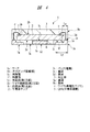
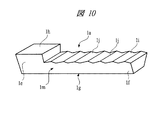
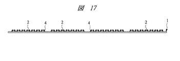
図1は本発明の実施の形態1の半導体装置の構造の一例を封止体を透過して示す斜視図、図2は図1に示す半導体装置の構造を示す断面図、図3は図1に示す半導体装置の短リードタイプの構造の一例を示す断面図、図4は図1に示す半導体装置の逆ボンディングタイプの構造の一例を示す断面図、図5は図1に示す半導体装置のリードの構造の一例を示す斜視図、図6および図7はそれぞれ図1に示す半導体装置の変形例のリードの構造を示す斜視図、図8は図1に示す半導体装置の逆台形のリードの構造の一例を示す斜視図、図9は図8に示すリードの構造を示す正面図、図10は図1に示す半導体装置の逆台形のリードの変形例の構造を示す斜視図、図11は図10に示すリードの構造を示す正面図、図12は図1に示す半導体装置の逆台形のリードの変形例の構造を示す斜視図、図13は図12に示すリードの構造を示す正面図、図14は本発明の実施の形態1の半導体装置の組み立てに用いられるリードフレームの構造の一例を示す平面図、図15は図14に示すリードフレームの構造を示す側面図、図16は本発明の実施の形態1の半導体装置の組み立てにおけるダイボンディング後の構造の一例を示す側面図、図17は本発明の実施の形態1の半導体装置の組み立てにおけるワイヤボンディング後の構造の一例を示す側面図、図18は本発明の実施の形態1の半導体装置の組み立てにおける樹脂モールディング時の構造の一例を示す部分断面図、図19は樹脂モールディング後の構造を示す斜視図、図20は本発明の実施の形態1の半導体装置の組み立てにおける個片化ダイシング時の構造の一例を示す斜視図、図21は図20に示す個片化ダイシング時の構造を示す断面図、図22は本発明の実施の形態1の半導体装置の組み立てにおける組み立て完了後の構造の一例を示す断面図、図28はワイヤボンディングにおける部分拡大断面図、図29はワイヤボンディング後の部分拡大断面図および部分拡大斜視図、図30は個片モールディングによる半導体装置の部分拡大断面図、図31は一括モールディングによる半導体装置の部分拡大断面図である。
(Embodiment 1)
1 is a perspective view showing an example of the structure of a semiconductor device according to
図1および図2に示す本実施の形態1の半導体装置は、樹脂封止型で、かつ小型の半導体パッケージであり、封止体3の裏面3aの周縁部に複数のリード1aそれぞれの実装面1gが露出して並べて配置されたノンリード型のものである。本実施の形態1では、前記半導体装置の一例として、QFN5を取り上げて説明する。なお、QFN5は、小型の半導体パッケージであるが、可能な限りパッケージサイズをチップサイズに近づけたものである。
The semiconductor device according to the first embodiment shown in FIGS. 1 and 2 is a resin-encapsulated and small-sized semiconductor package, and each mounting surface of a plurality of leads 1a on the peripheral portion of the
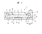
QFN5の構成について説明すると、その主面2bに半導体素子および複数のパッド(電極)2aを有する半導体チップ2と、半導体チップ2と接続するチップ搭載部であるタブ1bと、実装面(第1主面)1gとその反対側に配置されたワイヤ接続面(第2主面)1hとを有しており、かつワイヤ接続面1hを有する肉厚部(第1部分)1eと肉厚部1eより厚さが薄い肉薄部(第2部分)1fとを備え、さらにそれぞれワイヤ接続面1hの延在方向の長さが実装面1gより短く形成され、かつ、肉厚部1eにおける延在方向の長さが肉薄部1fにおける延在方向の長さよりも短く形成された複数のリード1aと、半導体チップ2の複数のパッド2aとこれに対応する複数のリード1aとをそれぞれ接続する複数の導電性ワイヤであるワイヤ4と、半導体チップ2および複数のワイヤ4を樹脂封止する封止体3とを有している。
The configuration of the
さらに、各リード1aは、その実装面1gが封止体3の裏面3aの周縁部に並んで配置されているとともに、各リード1aの肉薄部1fが、半導体チップ2の下部にもぐり込んで半導体チップ2の裏面2cと対向するように配置されている。
Furthermore, each lead 1a has its
このようにQFN5は、各リード1aの肉薄部1fを半導体チップ2の下部にもぐり込ませて配置することにより、封止体3の裏面3aに露出する各リード1aの実装面1gのリード延在方向の長さ(Lp)を確保して実装時の強度を保持しつつ、半導体チップ2の側面2dから封止体3の側面3bまでの距離(La)を可能な限り短くしてパッケージサイズをチップサイズに近づけてQFN5の小型化を図るものである。
In this way, the QFN 5 extends the lead 1a on the
したがって、各リード1aの肉厚部1eのワイヤ接続面1hのリード延在方向の長さは、ワイヤ4を接続するために必要な最低限の長さとし、本実施の形態1では、肉厚部1eにおける延在方向の長さが肉薄部1fにおける延在方向の長さよりも短く形成されている。このように、距離(La)ができるだけ短くなるようにしている。
Therefore, the length in the lead extending direction of the
なお、本実施の形態1のQFN5は、その組み立てにおいて図18に示すように、1枚のリードフレーム1の複数の装置形成領域を樹脂成形金型9の1つのキャビティ9cで覆って樹脂封止を行う一括モールディング方法を採用し、さらにその後ダイシングで個片化して組み立てたものである。したがって、封止体3の側面3bがリード1aの実装面1gに対してほぼ垂直に形成されるため、半導体チップ2の側面2dに隣接する封止体3の領域をその高さ方向に一律に距離(La)で形成することができ、これにより、半導体チップ2の側部においてワイヤ4を配置する領域を確保しやすい構造となっている。
In the assembly of the
そもそも封止体3の裏面3a側に露出するリード端子の長さは、QFN5を実装する実装基板、あるいはJEITAなどの規格として規定されている。このため、パッケージサイズの薄型化および小型化を図ろうとした場合、リード1aのワイヤ接続面側(リード1aにおいてタブ1bと隣接する端部)が半導体チップ2(特に裏面2c側の周縁部)と接触してしまう。そこで、本実施の形態1のように、リード1aのワイヤ接続面1h側において肉薄部1fを形成し、半導体チップ2とリード1aの接触を防止している。この時、単にリード1aを薄く形成すると、パッケージサイズの小型化に伴い、半導体チップ2の側面2dから封止体3の側面3bまでの距離が短く、その上、1stボンディング部と2ndボンディング部の高低差が大きくなるため、急峻な角度にワイヤボンディングすることになる。急峻な角度にワイヤボンディングすると、図28に示すように、1stボンディング側において、ワイヤボンディング技術により形成されるスタッドバンプからワイヤ4が引き出される根元部4aに応力が集中し、前記根元部4a付近で断線の原因となる。このように、断線の原因となる応力が生じないように、2ndボンディング側のワイヤ接続面1hは肉厚部1eとしてその厚みを残しておき、1stボンディング点と2ndボンディング点の高低差を低減する。ここで、パッケージサイズを十分に小型化にしたいため、ワイヤ接続面1hを有する肉厚部1eは、ワイヤボンディングが可能な領域(長さ)のみ設け、それ以外の領域は肉薄部1fとして薄く形成する。本実施の形態1では、肉厚部1eの領域(長さ)が肉薄部1fよりも小さく(狭く)形成されている。これにより、半導体チップ2とリード1aの接触を抑制し、かつ、パッケージサイズの小型化を図れる。
In the first place, the length of the lead terminal exposed on the
正ボンディングでワイヤ4を形成する場合、図29に示すように、2ndボンディング側はワイヤ4を引きちぎるようにリード1aのワイヤ接続面1hに圧着することから、1stボンディング側のボンディング面積よりも大きくなる。また、1つのデバイス領域1tを1つのテーパ付きのキャビディ9cで覆って樹脂封止する個片モールディングにより封止体3を形成すると、図23に示すように封止体3の側面3bは傾斜面となり、リード1aを金型でクランプした状態で樹脂封止するため、切断しろ1vが形成される。このため、2ndボンディングを打つためのワイヤ接続面1hの領域(長さ)Xが小さく(狭く)なる。
When the
この結果、図30に示すように2ndボンディングの際、ワイヤ端部4bが封止体3の側面3bから露出してしまい、ショート不良の原因となる。しかし、図2に示すような、一括モールディングにより封止体3を形成すれば、封止体3の側面3bは、リード1aのワイヤ接続面1hにほぼ垂直方向に形成され、かつ、リード1aのクランプ時に形成される切断しろ1vが形成されなくなるため、図31に示すように、2ndボンディングを打つリード1aのワイヤ接続面1hの領域(長さ)Yが図30に示すような個片モールディングタイプよりも広く確保(X<Y)できるため、封止体3の側面3bから露出するといった問題は抑制できる。
As a result, as shown in FIG. 30, the
また、各リード1aの肉薄部1fは、例えば、ハーフエッチング加工やプレス加工などによって肉厚部1eの1/2程度の厚さに薄く形成されたものである。例えば、リードフレーム1(図14参照)の厚さが、0.2mmの場合、各リード1aの肉厚部1eやタブ1bの厚さは、0.2mmとなり、肉薄部1fはその1/2程度の厚さとなる。これによって、半導体チップ2の裏面2cとリード1aの肉薄部1fとの間に樹脂を介在させて半導体チップ2の下部にリード1aの肉薄部1fをもぐり込ませることができる。
In addition, the
なお、各リード1aの肉薄部1fが半導体チップ2の裏面2c側に配置されるため、タブ1bは各リード1aの肉薄部1fと干渉しないように半導体チップ2の大きさより小さく形成された小タブ構造のものである。
Since the
QFN5では、半導体チップ2は、その厚さと交差する平面は四角形であり、例えば、シリコンなどによって形成され、その裏面2cがダイボンド材6によってタブ1bの主面1cと接合されて固定されている。
In the
また、各リード1aやタブ1bは、例えば、銅合金によって形成され、さらに、ワイヤ4は、例えば、金線であり、封止体3は、例えば、熱硬化性のエポキシ樹脂などから成る。
Each lead 1a and
図2に示すQFN5では、リード1aの実装面1gのリード延在方向の長さ(Lp)は、例えば、標準的な0.6mmであり、その際、半導体チップ2の側面2dから封止体3の側面3bまでの距離(La)を0.35mm程度に短くすることができる。
In the
また、図3に示す短リードタイプのQFN5のように、図2のQFN5と同様の構造においてさらに短いリード1aを採用することにより、リード1aの長さ(Lp)を、例えば、0.45mmにすることができる。 Further, by adopting a shorter lead 1a in the same structure as the QFN5 of FIG. 2, such as the short lead type QFN5 shown in FIG. 3, the length (Lp) of the lead 1a is, for example, 0.45 mm. can do.
本実施の形態1のQFN5では、各リード1aの薄く形成された肉薄部1fが、半導体チップ2の下部にもぐり込んで配置されていることにより、各リード1aの実装面1gのリード延在方向の長さ(Lp)を確保して実装時の接続強度を保持しつつ、半導体チップ2の側面2dから封止体3の側面3bまでの距離(La)をできる限り短くしてパッケージサイズをチップサイズに近づけ、これによって、QFN5の小型化を図ることができる。
In the
なお、QFN5における半導体チップ2の側部の領域の水平方向の長さの規定としては、例えば、リード1aの延在方向に平行な方向のワイヤ接続面1hの長さを、実装面1gの同方向の長さの1/2以下にすることにより、QFN5の小型化を図ることができる。あるいは、半導体チップ2の側面2dから封止体3の側面3bまでの距離(La)を、0.35mm以下にすることにより、QFN5の小型化を図ることができる。
The horizontal length of the side region of the
また、本実施の形態1のQFN5では、各リード1aの肉薄部1fが、半導体チップ2の下部にもぐり込んで配置されていることにより、肉薄部1fが肉厚部1eより薄く形成されている分、封止体3の厚さを薄くしてQFN5の薄型化を図ることができる。
Further, in the
さらに、QFN5では、タブ1bが、その裏面1dが封止体3の裏面3aに露出するように配置されているため、半導体チップ2から発せられる熱をタブ1bから外部に放散させることができ、QFN5の放熱性を向上させることができる。また、タブ1bが封止体3の裏面3aに露出しているため、実装基板への実装時にタブ1bをGND接続に用いることにより、QFN5のGND強化を図ってGNDを安定化させることができる。
Furthermore, in QFN5, the
また、タブ1bが封止体3の裏面3aに露出するように配置されているため、QFN5の薄型化を図ることができる。
Further, since the
次に、図4に示すQFN5の構造について説明する。
Next, the structure of
図4に示すQFN5は、逆ボンディングタイプの構造のものであり、図3に示すQFN5をチップサイズを変えることなく、さらに小型化を図るものである。
The
図2および図3に示すQFN5では、ワイヤボンディングの際に、まず半導体チップ2側を先に接続し、その後リード1a側を接続する正ボンディング方法を採用しているのに対して、図4に示すQFN5は、ワイヤボンディングの際に、まずリード1a側を先に接続し、その後半導体チップ2側を接続する逆ボンディング方法を採用している。
The
ワイヤボンディングでは、先に接続する側(以降、1stボンディング側という)は、被接続面に対してほぼ垂直にワイヤ4を立ち上げることができ、さらに、前記被接続面において必要とされるボンディング面積は、後に接続する側(以降、2ndボンディング側という)に比較して小さくすることが可能なため、この特性を利用してワイヤボンディングの際にリード1a側に1stボンディングを行い、これによって、リード1aの肉厚部1eにおけるワイヤ接続面1hの長さをワイヤボンディング技術により形成されるスタッドバンプとほぼ同等の長さ(幅)にまで縮小にすることができる。また、上記で説明したように、ワイヤ4は1stボンディング側に形成されるスタッドバンプからリード1aのワイヤ接続面1hにほぼ垂直方向に立ち上げる(引き出される)ため、ワイヤ4の根元部4aにかかる応力が、正ボンディング方法に比べて低減できる。このように、半導体チップ2の側面2dから封止体3の側面3bまでの距離(La)を最小にし、かつ、1stボンディング側のワイヤ4の根元部4aに生じる応力を低減することができる。
In wire bonding, the side to be connected first (hereinafter referred to as the first bonding side) can raise the
なお、その際においても各リード1aの実装面1gのリード延在方向の長さ(Lp)は、例えば、Lp=0.45mmを確保しており、基板実装時の接続強度は保持している。
Even in this case, the length (Lp) in the lead extending direction of the mounting
したがって、図4に示すQFN5のように、一括モールディング方法と逆ボンディング方法を採用することにより、QFN5における距離(La)を最小にして図2および図3に示す構造よりも、さらにQFN5の小型化を図ることができる。図4に示すQFN5では、距離(La)は、例えば、0.30mm程度である。
Therefore, by adopting the batch molding method and the reverse bonding method as in QFN5 shown in FIG. 4, the distance (La) in QFN5 is minimized and the size of QFN5 is further reduced as compared with the structure shown in FIGS. Can be achieved. In the
なお、図4に示すQFN5では、ワイヤボンディングの2ndボンディング側が半導体チップ2側であるため、2ndボンディングではワイヤ4と半導体チップ2のパッド2aとを接続することになる。半導体チップ2のパッド2aの表面はアルミ層であるため、ワイヤ4が金線である場合には、予めパッド2a上に金バンプ7を接続しておき、図4に示すように、2ndボンディングの際にこの金バンプ7にワイヤ4を接続するようにしてもよい。このように、2ndボンディングでワイヤ4と半導体チップ2のアルミニウムのパッド2aとを接続するような場合には、予めパッド2a上に金バンプ7を接続しておき、この金バンプ7とワイヤ4とを接続することにより、ワイヤ4とパッド2aとの接続信頼性をより高めることができる。
In the
ただし、パッド2aに対して直接ワイヤ4を接続しても接続信頼性上特に問題がなければ、金バンプ7を用いずに直接ワイヤ4とパッド2aとを接続してもよい。
However, if there is no particular problem in connection reliability even if the
なお、パッド2a上に金バンプ7を形成する際には、ワイヤボンディング技術を利用したスタッドバンプ形成方法で形成することが好ましい。
In addition, when forming the
次に、QFN5における種々のリード形状について説明する。図5は、図1に示すQFN5に組み込まれたリード1aの形状の一例を示しており、肉厚部1eと肉薄部1fとからなり、肉厚部1eはワイヤ接続面(第2主面)1hを有している。一方、肉厚部1eより厚さが薄い肉薄部1fは、段差面(第3主面)1iを有している。
Next, various lead shapes in the
これに対して図6に示す変形例のリード1aは、その肉薄部1fの段差面1iに、波形状の凹凸1jが形成されている。これにより、リード1aと封止用樹脂(図18参照)8との接触面積を増やしてリード1aと封止用樹脂8の密着度を高めることができる。さらに、凹凸1jが形成されたことにより、リード1aの延在方向に対する封止体3からの引き抜き強度を高めることができ、リード1aの封止体3からの脱落を低減することができる。
On the other hand, the lead 1a of the modification shown in FIG. 6 has a wave-shaped
また、図7に示す変形例のリード1aは、その肉薄部1fの段差面1iに、複数の窪み部であるディンプル1kが形成されており、前記凹凸1jの場合と同様に、リード1aと封止用樹脂8との接触面積を増やしてリード1aと封止用樹脂8の密着度を高めることができ、さらに、パッケージ水平方向に対する封止体3からの引き抜き強度を高めて、リード1aの封止体3からの脱落を低減することができる。
Further, the lead 1a of the modification shown in FIG. 7 has a plurality of
また、図8〜図13に示すリード1aは、図5、図6および図7に示すリード1aに対して、それぞれリード1aの延在方向に対する直角な方向の幅を、実装面1gよりワイヤ接続面1hまたは段差面1iの方が広くなるように形成したものである。すなわち、図9、図11および図13に示すようにそれぞれのリード1aが実装面1gに向けて幅狭になるように形成されており、各リード1aの長手方向の側部の面が傾斜面1mとなっている。したがって、各リード1aの正面形状が逆台形になるように形成されており、これにより、リード1aの厚さ方向に対する封止体3からの引き抜き強度を高めて、リード1aの封止体3からの脱落を低減することができる。
Further, the lead 1a shown in FIGS. 8 to 13 is connected to the lead 1a shown in FIGS. 5, 6, and 7 in a width direction perpendicular to the extending direction of the lead 1a from the mounting
前記特許文献1(特開2003−37219号公報)の構造の場合、インナーリード部において2ndボンディング点から封止体の側面の間に、樹脂とリードの密着性を向上させる目的で凹部が形成されている。このため、個片モールディングにより封止体を形成しても、2ndボンディング点から封止体の側面までの距離が十分に確保されているため、封止体の側面から露出することはない。しかし、この構造では、よりチップサイズに近いパッケージサイズを実現できない。 In the case of the structure of Patent Document 1 (Japanese Patent Laid-Open No. 2003-37219), a recess is formed between the 2nd bonding point and the side surface of the sealing body in the inner lead portion for the purpose of improving the adhesion between the resin and the lead. ing. For this reason, even if the sealing body is formed by individual molding, the distance from the 2nd bonding point to the side surface of the sealing body is sufficiently secured, so that it is not exposed from the side surface of the sealing body. However, with this structure, a package size closer to the chip size cannot be realized.
これに対し、本実施の形態1ではワイヤ接続面1hを有する肉厚部1eは、ワイヤボンディングが可能な領域(長さ、幅)のみ設けられるため、ワイヤ接続面1h上に、例えば樹脂との密着性を向上するための凹部(溝)など形成できないことから、リード1aの密着度強化のためには、図6乃至図13に示すような構造が効果的である。また凹部(溝)をワイヤ接続面1h上に形成しない分、パッケージサイズの小型化が実現できる。
On the other hand, in the first embodiment, the thick portion 1e having the
次に、本実施の形態1のQFN5(半導体装置)の製造方法について説明する。 Next, a method for manufacturing QFN 5 (semiconductor device) according to the first embodiment will be described.
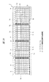
まず、図14および図15に示すように複数のデバイス領域(装置形成領域)1tが区画形成されたリードフレーム1を準備する。なお、1つのデバイス領域1tは、実装面1gとその反対側に配置されたワイヤ接続面1hとを有しており、かつワイヤ接続面1hを有する肉厚部1eと肉厚部1eより厚さが薄い肉薄部1fとを備えており、さらにそれぞれワイヤ接続面1hのリード延在方向の長さが実装面1gより短く形成された複数のリード1aと、複数のリード1aの内側に配置されたチップ搭載部であるタブ1bとを含んでいる。肉薄部1fは、ハーフエッチング加工やプレス加工によって肉厚部1eよりその厚さを薄く形成したものである。
First, as shown in FIGS. 14 and 15, a
また、リードフレーム1には、区画形成された複数のデバイス領域1tの外側の枠部1uに、応力緩和用の第1スリット1n、樹脂通過用の第2スリット1p、フレームの反り防止用の長スリット1q、搬送用のガイド孔1rおよび位置決め孔1sがそれぞれ複数形成されている。
Further, the
その後、図16に示すようにダイボンディングを行う。ここでは、リードフレーム1のタブ1bの主面1c上にダイボンド材6を介して半導体チップ2を搭載し、半導体チップ2を固着する。その際、半導体チップ2の裏面2cとリード1aの肉薄部1fとが対向するように半導体チップ2をタブ1bに搭載する。
Thereafter, die bonding is performed as shown in FIG. Here, the
ダイボンディング後、図17に示すように、ワイヤボンディングを行う。すなわち、半導体チップ2のパッド2aとリード1aの肉厚部1eのワイヤ接続面1hとをワイヤ4で接続する。
After die bonding, wire bonding is performed as shown in FIG. That is, the
その際、図4に示すような逆ボンディングを採用する場合には、まず、先にリード1aの肉厚部1eのワイヤ接続面1hとワイヤ4とをワイヤボンディングする。これにより、1stボンディング側は、被接続面に対してほぼ垂直にワイヤ4を立ち上げた状態で接続を完了できるため、リード1aのワイヤ接続面1hに対してほぼ垂直にワイヤ4を立ち上げて接続することができる。
At that time, when reverse bonding as shown in FIG. 4 is employed, first, the
また、1stボンディング側は、2ndボンディング側よりそのボンディングに必要な面積が小さくて済むため、これにより、ワイヤ接続面1hにほぼ垂直にワイヤ4を立ち上げることができるとともに、リード1aの肉厚部1eのワイヤ接続面1hを最小にすることができ、さらにこのワイヤ接続面1hにほぼ垂直にワイヤ4を立ち上げることができるため、半導体チップ2の側面2dから封止体3の側面3bまでの距離(La)を最小とし、かつ、1stボンディング側のワイヤ4の根元部4aに生じる応力を低減することができる。
Further, since the first bonding side requires a smaller area than the 2nd bonding side, the
1stボンディング終了後、ワイヤ4と半導体チップ2のパッド2aとを接続する2ndボンディングを行う。その際、ワイヤ4と、半導体チップ2のパッド2a上に予め接続された金バンプ7とを接続する。ただし、金バンプ7は、必ずしも用いなくてもよい。
After the completion of the 1st bonding, 2nd bonding for connecting the
なお、ワイヤボンディングとして、正ボンディング、すなわち半導体チップ2側を1stボンディングしてリード1a側を2ndボンディングする場合には、図3に示すように、まず、1stボンディングとして半導体チップ2のパッド2aとワイヤ4とを接続し、その後、2ndボンディングとしてリード1aの肉厚部1eのワイヤ接続面1hとワイヤ4とを接続する。
When wire bonding is positive bonding, that is, when 1st bonding is performed on the
ワイヤボンディング終了後、樹脂モールディングを行う。すなわち、封止体3の裏面3aの周縁部に複数のリード1aそれぞれの実装面(第1の主面)1gが露出するように半導体チップ2と複数のワイヤ4を樹脂封止して封止体3を形成する。タブ露出構造の場合には、封止体3の裏面3aにタブ1bも露出するように樹脂封止する。
Resin molding is performed after wire bonding. That is, the
本実施の形態1では、樹脂封止工程で、リードフレーム1上に区画形成された複数のデバイス領域(装置形成領域)1tを樹脂成形金型の1つのキャビティで覆って前記樹脂封止を行う一括モールディング方法で樹脂封止する。その際、図18に示すように、樹脂成形金型9の上型9aの金型面9d上にリードフレーム1を配置し、リードフレーム1上に区画形成された複数のデバイス領域1tを所望の区画数ごとに樹脂成形金型9の上型9aの複数のキャビティ9cそれぞれで覆って樹脂封止する。すなわち、所定数のデバイス領域1tを含んだブロック単位を1つのキャビティ9cで覆ってブロック単位ごとに分けた状態での一括モールディングを行う。ただし、この際、複数のリード1aそれぞれの実装面(第1主面)1gが露出するようにフィルムシート14などを採用しリード1a端子面を覆い、露出端子面へのモールド樹脂漏れを防ぐ方法が取られる。
In the first embodiment, in the resin sealing step, the resin sealing is performed by covering a plurality of device regions (device forming regions) 1t partitioned and formed on the
このようにブロック単位ごと分けて1つのキャビティ9cで覆って一括モールディングを行うことにより、図19に示すように、1枚のリードフレーム1上に複数に分割した一括封止体10を形成することができ、樹脂(例えば、熱硬化性のエポキシ樹脂)と金属(例えば、銅合金)との熱収縮量の差によりリードフレーム1上で発生する応力を分散させることができ、リードフレーム1における反りを低減することができる。
As shown in FIG. 19, a
樹脂封止後、リードフレーム1から複数のリード1aそれぞれを分離して個片化を行う。ここでは、図20および図21に示すように、ブレード11を用いてダイシングによって個片化を行い、これにより、図22に示すようなQFN5の組み立て完了となる。
After the resin sealing, the plurality of leads 1a are separated from the
このように本実施の形態1では、リード1aのワイヤ接続面1hが実装面1gより短く形成されたリードフレーム1を用い、半導体チップ2の裏面2cとリード1aの肉薄部1fとが対向するように半導体チップ2をタブ1b上に搭載して組み立てることにより、図2や図3に示すように、半導体チップ2の側面2dから封止体3の側面3bまでの距離(La)を短くすることができ、その結果、パッケージサイズをチップサイズに近づけてQFN5の小型化を図ることができる。
As described above, in the first embodiment, the
さらに、ワイヤボンディングにおいて先にリード1aのワイヤ接続面(第2の主面)1hとワイヤ4とを接続し、その後、ワイヤ4と半導体チップ2のパッド2aとを接続(逆ボンディング)することにより、リード1aの実装面1gを短くすることなく、逆ボンディングによって図4に示すように半導体チップ2の側面2dと封止体3の側面3bの距離(La)をさらに短くすることができる。
Further, in wire bonding, the wire connection surface (second main surface) 1h of the lead 1a is first connected to the
その結果、封止体3の裏面3aに露出するリード1aの実装面1gを短くせずにパッケージサイズをよりチップサイズに近づけることが可能になり、基板実装後の接続強度や電気的特性を低下させることなくQFN5の小型化を図ることができる。すなわち、パッケージサイズをチップサイズにより近づけてQFN5の小型化を図ることが可能になる。
As a result, the package size can be made closer to the chip size without shortening the mounting
なお、本実施の形態1で説明したように一括モールディングによって樹脂封止を行うことにより、逆ボンディングを行った際には、リード1aのワイヤ接続面1hにほぼ垂直にワイヤ4を立ち上げることができるため、一括モールディングおよびその後のダイシングによる個片化でリード1aのワイヤ接続面1h上(半導体チップ2の側部)に一律な幅で封止体3を形成することができ、これにより、逆ボンディングによってワイヤ接続面1h上にほぼ垂直に立ち上がったワイヤ4を十分に樹脂で覆うことができる。
As described in the first embodiment, by performing resin sealing by batch molding, when reverse bonding is performed, the
さらに、一括モールディングは、正ボンディング(1stボンディングを半導体チップ2に対して行って、2ndボンディングをリード1aに対して行うワイヤボンディング)の場合においても有効である。
Furthermore, batch molding is also effective in the case of positive bonding (wire bonding in which 1st bonding is performed on the
すなわち、一括モールディングと正ボンディングを組み合わせた場合、正ボンディングにおける2ndボンディングはリード1aのワイヤ接続面1hに対して行うが、その際、図23に示すような個片モールディング(1つのデバイス領域1tを1つのキャビティ9cで覆って樹脂封止する方法)タイプの半導体装置では、リード1aのワイヤ接続面1hの外側端部に切断しろ1vが必要になるため、ワイヤ接続面1hが狭くなり、2ndボンディング側のボンディング条件が厳しくなる。これに対して一括モールディングでは、図22に示すようにリード1aのワイヤ接続面1hが外側端部ぎりぎりまで樹脂で覆われるため、リード1aのワイヤ接続面1hに対する2ndボンディング側のボンディング条件に余裕ができる。
That is, when batch molding and positive bonding are combined, 2nd bonding in the positive bonding is performed on the
したがって、一括モールディングは、ワイヤ接続面1hが小さなリード1aに対して非常に有効であるとともに、正ボンディングまたは逆ボンディングに対しても非常に有効である。
Therefore, collective molding is very effective for the lead 1a having a small
(実施の形態2)
図23は本発明の実施の形態2の半導体装置の構造の一例を示す断面図、図24は本発明の実施の形態2の半導体装置の組み立てにおける個片化切断時の構造の一例を示す断面図である。
(Embodiment 2)
23 is a cross-sectional view showing an example of the structure of the semiconductor device according to the second embodiment of the present invention, and FIG. 24 is a cross-section showing an example of the structure at the time of singulation cutting in the assembly of the semiconductor device according to the second embodiment of the present invention. FIG.
本実施の形態2の半導体装置は、実施の形態1のQFN5と同様に、パッケージサイズをチップサイズに近づけたQFN12であるが、樹脂封止工程で個片モールディングが行われ、さらに、個片化工程で図24に示すような切断金型13を用いて切断が行われて個片化された半導体装置である。
The semiconductor device of the second embodiment is a
すなわち、図23に示すQFN12は、実施の形態1のQFN5と同様にそれぞれに肉薄部1fと肉厚部1eを有する複数のリード1aを有しており、かつ半導体チップ2の裏面2cと各リード1aの肉薄部1fとが対向して配置され、各リード1aの肉薄部1fを半導体チップ2の裏面2c側にもぐり込ませたことにより、半導体チップ2の側面2dと封止体3の側面3bとの距離を短くするとともに、ワイヤボンディングで逆ボンディングを行ってパッケージサイズをチップサイズに近づけてその小型化を図ることができる。
That is, the
QFN12の組み立てでは、ワイヤボンディングの際に、1stボンディングとしてリード1aの肉厚部1eのワイヤ接続面1hにワイヤ4を接続し、その後、2ndボンディングとして半導体チップ2のパッド2aにワイヤ4を接続する逆ボンディングを行う。さらに、ワイヤボンディング後、個片モールディングによって樹脂封止を行って封止体3を形成する。
In the assembly of the
実施の形態1では、逆ボンディングによりワイヤボンディングした後、一括モールド方法により封止体3を形成したQFN5について説明したが、上記したように、逆ボンディングによりワイヤボンディングを行うと、半導体チップ2の側面2dから封止体3の側面3bまでの距離(La)を低減できる。言い換えると、個片モールディングにより切断しろ1vや封止体3の側面3bが傾斜面(テーパ)となるように形成されると、ワイヤ接続面1hの長さ(幅)が短くなるが、逆ボンディングによるワイヤボンディングの場合、1stボンディング側のボンディング面積を2nd側のボンディング面積よりも低減できるため、個片モールディングにより形成された封止体3の側面3bから半導体チップ2の側面2dまでの距離が狭くなっても、封止体3の側面3bからワイヤ4が露出することなく形成できる。
In the first embodiment, the
樹脂封止工程後、個片化工程で、図24に示す切断金型13を用いて個片化を行う。その際、切断金型13の上型13aと下型13bによってリードフレーム1を挟持し、切断刃13cによってリード切断を行う。なお、下型13bの支持部13fでリードフレーム1を支持する箇所の先端の幅は、0.1mm程度であり、したがって、図23に示す各リード1aの切断しろ1vも0.1mm程度である。
After the resin sealing step, in the individualization step, individualization is performed using the cutting
リード1aの切断では、まず、ゲートに相当する1つの角部で切断(ゲートカット)を行う。次に、残る3箇所の角部でリード切断(ピンチカット)を行い、さらに、2方向のうちの何れか一方の方向の辺に対応して設けられた複数のリード1aの切断(X側のリード先端カット)を行う。その後、2方向のうちの何れか他方の方向の辺に対応して設けられた複数のリード1aの切断(Y側のリード先端カット)を行う。すなわち、リード切断では、4つの工程に分けてリード切断を行う。 In cutting the lead 1a, first, cutting (gate cutting) is performed at one corner corresponding to the gate. Next, lead cutting (pinch cutting) is performed at the remaining three corners, and a plurality of leads 1a provided corresponding to sides in one of two directions (cutting on the X side) Cut the lead tip. Thereafter, the plurality of leads 1a provided corresponding to the side in either one of the two directions are cut (Y-side lead tip cut). That is, in lead cutting, lead cutting is performed in four steps.
なお、切断金型13の上型13aおよび下型13bには、それぞれ逃げ部13d,13eが設けられている。つまり、逃げ部13d,13eが設けられたことにより、上型13aと封止体3、および下型13bと封止体3との間にそれぞれ隙間が形成され、特にリード切断時には、リード1aや樹脂などの切断くずが下型13bと封止体3との間に挟まれることなく逃げ部13eに落下させることができる。これにより、前記切断くずによって封止体3に傷が形成されることを防止できる。
The
また、上型13aの逃げ部13dは、タブ1bを逃げた形状となっており、リード切断時にリード1aのみを押さえるように形成されている。これにより、リード切断時にはタブ1bにはプレッシャーが付与されず、半導体チップ2へのプレッシャーの付与を避けることができる。
Further, the
このようにしてリード切断を行い、図23に示すQFN12の組み立てを完了する。
In this way, lead cutting is performed to complete the assembly of the
実施の形態2のQFN12のように、個片モールディングを行って、その後、リード切断による個片化を行ってもパッケージサイズをチップサイズに近づけてQFN12の小型化を図ることができる。
Even if individual molding is performed and then individualization by lead cutting is performed as in the
以上、本発明者によってなされた発明を発明の実施の形態に基づき具体的に説明したが、本発明は前記発明の実施の形態に限定されるものではなく、その要旨を逸脱しない範囲で種々変更可能であることは言うまでもない。 Although the invention made by the present inventor has been specifically described based on the embodiments of the invention, the present invention is not limited to the embodiments of the invention, and various modifications can be made without departing from the scope of the invention. It goes without saying that it is possible.
例えば、前記実施の形態1では、一括モールディングとして、ブロック単位ごとに分けてそれぞれブロックごとに1つのキャビティ9cで複数のデバイス領域1tを覆って一括モールディングを行う場合を説明したが、前記一括モールディングとしては、ブロックごとに分けずにリードフレーム1上に形成された全てのデバイス領域1tを1つのキャビティ9cで覆って一括モールディングを行ってもよい。
For example, in the first embodiment, a case has been described in which batch molding is performed by covering a plurality of device regions 1t with one
また、前記本実施の形態1および2では、タブ1bが封止体3の裏面3aから露出する構造について説明したが、図25〜図27に示すように、タブ1bをその裏面1dから主面1cに向ってハーフエッチングを施し、封止体3内にタブ1bを内蔵させてもよい。タブ1bを封止体3に内蔵させることで、QFN5を実装する実装基板側での配線パターンの引き回しできる領域が、タブ1bを封止体3の裏面3aから露出する場合に比べて広くなり、自由度を向上できる。
In the first and second embodiments, the structure in which the
本発明は、電子装置および半導体装置の製造技術に好適である。 The present invention is suitable for manufacturing techniques of electronic devices and semiconductor devices.
1 リードフレーム
1a リード
1b タブ(チップ搭載部)
1c 主面
1d 裏面
1e 肉厚部
1f 肉薄部
1g 実装面(第1主面)
1h ワイヤ接続面(第2主面)
1i 段差面(第3主面)
1j 凹凸
1k ディンプル(窪み部)
1m 傾斜面
1n 第1スリット
1p 第2スリット
1q 長スリット
1r ガイド孔
1s 位置決め孔
1t デバイス領域(装置形成領域)
1u 枠部
1v 切断しろ
2 半導体チップ
2a パッド(電極)
2b 主面
2c 裏面
2d 側面
3 封止体
3a 裏面
3b 側面
4 ワイヤ(導電性ワイヤ)
4a 根元部
4b ワイヤ端部
5 QFN(半導体装置)
6 ダイボンド材
7 金バンプ
8 封止用樹脂
9 樹脂成形金型
9a 上型
9b 下型
9c キャビティ
9d 金型面
10 一括封止体
11 ブレード
12 QFN(半導体装置)
13 切断金型
13a 上型
13b 下型
13c 切断刃
13d,13e 逃げ部
13f 支持部
14 フィルムシート
1 Lead
1h Wire connection surface (second main surface)
1i Step surface (third main surface)
1j Concavity and
1m inclined surface 1n
1u
6
13
Claims (16)
前記半導体チップの外形寸法よりも小さいチップ搭載部と、
第1主面と、前記第1主面と反対側の第2主面と、前記第1主面と前記第2主面との間
に位置する第3主面と、を有し、前記チップ搭載部の周囲に配置された複数のリードと、
前記半導体チップの前記複数の電極と前記複数のリードとをそれぞれ電気的に接続する複数のワイヤと、
前記半導体チップ、前記複数のワイヤ、前記複数のリードの一部を封止する封止体と、を含み、
前記リードは、前記チップ搭載部から前記封止体の各辺に向かう方向に延在しており、
前記リードの前記第1主面は、前記封止体の裏面より露出しており、
前記ワイヤは、前記リードの前記第2主面に接続されており、
前記リードは、前記第3主面が前記半導体チップの前記裏面と対向するように配置されており、
前記リードの前記第2主面の延在方向の長さは、前記第3主面の延在方向の長さよりも短いことを特徴とする半導体装置。 A semiconductor chip having a surface on which a plurality of electrodes are formed, and a back surface opposite to the surface;
A chip mounting portion smaller than the outer dimensions of the semiconductor chip;
A chip having a first main surface, a second main surface opposite to the first main surface, and a third main surface located between the first main surface and the second main surface. A plurality of leads arranged around the mounting portion;
A plurality of wires that electrically connect the plurality of electrodes and the plurality of leads of the semiconductor chip, and
A sealing body that seals part of the semiconductor chip, the plurality of wires, and the plurality of leads,
The lead extends in a direction from the chip mounting portion toward each side of the sealing body,
The first main surface of the lead is exposed from the back surface of the sealing body,
The wire is connected to the second main surface of the lead;
The lead is disposed such that the third main surface faces the back surface of the semiconductor chip,
The length of the lead in the extending direction of the second main surface of the lead is shorter than the length of the third main surface in the extending direction.
前記リードの前記第2主面上には、凹部や溝が形成されていないことを特徴とする半導体装置。 The semiconductor device according to claim 1,
A semiconductor device is characterized in that no recess or groove is formed on the second main surface of the lead.
前記リードの前記第1主面から前記第3主面までのリード厚が、前記第1主面から前記第2主面までのリード厚よりも薄いことを特徴とする半導体装置。 The semiconductor device according to claim 1,
A semiconductor device, wherein a lead thickness of the lead from the first main surface to the third main surface is smaller than a lead thickness from the first main surface to the second main surface.
前記第1主面から前記第3主面までのリード厚は、前記第1主面から前記第2主面までのリード厚の1/2程度であることを特徴とする半導体装置。 The semiconductor device according to claim 1,
A semiconductor device, wherein a lead thickness from the first main surface to the third main surface is about ½ of a lead thickness from the first main surface to the second main surface.
前記リードの前記第2主面の領域は、前記第3主面の領域よりも狭く形成されていることを特徴とする半導体装置。 The semiconductor device according to claim 1,
An area of the second main surface of the lead is formed narrower than an area of the third main surface.
前記ワイヤと前記半導体チップの前記電極とは、前記半導体チップの前記電極上に形成されたバンプを介して接続されていることを特徴とする半導体装置。 The semiconductor device according to claim 1,
The semiconductor device, wherein the wire and the electrode of the semiconductor chip are connected via a bump formed on the electrode of the semiconductor chip.
前記リードの延在方向とは直角な方向の前記第2主面の幅は、前記リードの前記第1主面の幅よりも広いことを特徴とする半導体装置。 The semiconductor device according to claim 1,
The width of the second main surface in a direction perpendicular to the extending direction of the lead is wider than the width of the first main surface of the lead.
前記リードの延在方向とは直角な方向の前記第3主面の幅は、前記リードの前記第1主面の幅よりも広いことを特徴とする半導体装置。 The semiconductor device according to claim 1,
The width of the third main surface in a direction perpendicular to the extending direction of the lead is wider than the width of the first main surface of the lead.
前記リードの延在方向とは直角な方向の前記第2主面の幅は、前記リードの前記第3主面の幅よりも広いことを特徴とする半導体装置。 The semiconductor device according to claim 1,
The width of the second main surface in a direction perpendicular to the extending direction of the leads is wider than the width of the third main surface of the leads.
前記第2主面の延在方向の長さは、前記第1主面の延在方向の長さの1/2以下であることを特徴とする半導体装置。 The semiconductor device according to claim 1,
Before SL length in the extending direction of the second main surface, wherein a said first major surface of the extending direction is 1/2 or less of the length.
前記封止体の側面は、前記リードの前記第2主面に対して垂直方向に形成されていることを特徴とする半導体装置。 The semiconductor device according to claim 1,
Side of the front Kifutometai A semiconductor device characterized by being formed in a direction perpendicular to the second major surface of the lead.
前記リードの前記第2主面は、前記封止体の前記側面から露出していないことを特徴とする半導体装置。 The semiconductor device according to claim 11.
The semiconductor device according to claim 1, wherein the second main surface of the lead is not exposed from the side surface of the sealing body.
前記半導体チップの外形寸法よりも小さいチップ搭載部と、
第1主面と、前記第1主面と反対側の第2主面と、を有し、前記チップ搭載部の周囲に配置された複数のリードと、
前記半導体チップの前記複数の電極と前記複数のリードとをそれぞれ電気的に接続する複数のワイヤと、
前記半導体チップ、前記複数のワイヤ、前記複数のリードの一部を封止する封止体と、を含み、
前記リードは、第1部分と、前記第1部分よりもリード厚が薄い第2部分と、を有し、前記チップ搭載部から前記封止体の各辺に向かう方向に延在しており、
前記リードの前記第1主面は、前記封止体の裏面より露出しており、
前記ワイヤは、前記リードの前記第1部分における前記第2主面に接続されており、
前記リードは、前記第2部分における前記第2主面が前記半導体チップの前記裏面と対向するように配置されており、
前記リードの前記第1部分における前記第2主面の延在方向の長さは、前記第2部分における前記第2主面の延在方向の長さよりも短いことを特徴とする半導体装置。 A semiconductor chip having a surface on which a plurality of electrodes are formed, and a back surface opposite to the surface;
A chip mounting portion smaller than the outer dimensions of the semiconductor chip;
A plurality of leads having a first main surface and a second main surface opposite to the first main surface, and disposed around the chip mounting portion;
A plurality of wires that electrically connect the plurality of electrodes and the plurality of leads of the semiconductor chip, and
A sealing body that seals part of the semiconductor chip, the plurality of wires, and the plurality of leads,
The lead has a first portion and a second portion having a lead thickness thinner than the first portion, and extends in a direction from the chip mounting portion toward each side of the sealing body,
The first main surface of the lead is exposed from the back surface of the sealing body,
The wire is connected to the second major surface of the first portion of the lead;
The lead is disposed such that the second main surface of the second portion faces the back surface of the semiconductor chip;
The length of the second main surface in the extending direction of the first portion of the lead is shorter than the length of the second main surface in the extending direction of the second portion.
前記リードの前記第1部分における前記第2主面上には、凹部や溝が形成されていないことを特徴とする半導体装置。 The semiconductor device according to claim 15, wherein
A semiconductor device is characterized in that no recess or groove is formed on the second main surface of the first portion of the lead.
Priority Applications (6)
| Application Number | Priority Date | Filing Date | Title |
|---|---|---|---|
| JP2004285839A JP4525277B2 (en) | 2004-09-30 | 2004-09-30 | Semiconductor device |
| TW094128043A TWI431738B (en) | 2004-09-30 | 2005-08-17 | A manufacturing method of a semiconductor device |
| CNB2005100986435A CN100446201C (en) | 2004-09-30 | 2005-09-05 | Manufacturing method of a semiconductor device |
| US11/222,959 US7323366B2 (en) | 2004-09-30 | 2005-09-12 | Manufacturing method of a semiconductor device |
| KR1020050086272A KR101160694B1 (en) | 2004-09-30 | 2005-09-15 | Manufacturing Method of Semiconductor Device |
| US12/014,313 US7728412B2 (en) | 2004-09-30 | 2008-01-15 | Semiconductor device having plurality of leads |
Applications Claiming Priority (1)
| Application Number | Priority Date | Filing Date | Title |
|---|---|---|---|
| JP2004285839A JP4525277B2 (en) | 2004-09-30 | 2004-09-30 | Semiconductor device |
Related Child Applications (1)
| Application Number | Title | Priority Date | Filing Date |
|---|---|---|---|
| JP2009274068A Division JP2010050491A (en) | 2009-12-02 | 2009-12-02 | Method of manufacturing semiconductor device |
Publications (3)
| Publication Number | Publication Date |
|---|---|
| JP2006100636A JP2006100636A (en) | 2006-04-13 |
| JP2006100636A5 JP2006100636A5 (en) | 2007-10-25 |
| JP4525277B2 true JP4525277B2 (en) | 2010-08-18 |
Family
ID=36145875
Family Applications (1)
| Application Number | Title | Priority Date | Filing Date |
|---|---|---|---|
| JP2004285839A Active JP4525277B2 (en) | 2004-09-30 | 2004-09-30 | Semiconductor device |
Country Status (5)
| Country | Link |
|---|---|
| US (2) | US7323366B2 (en) |
| JP (1) | JP4525277B2 (en) |
| KR (1) | KR101160694B1 (en) |
| CN (1) | CN100446201C (en) |
| TW (1) | TWI431738B (en) |
Families Citing this family (20)
| Publication number | Priority date | Publication date | Assignee | Title |
|---|---|---|---|---|
| US7001798B2 (en) * | 2001-11-14 | 2006-02-21 | Oki Electric Industry Co., Ltd. | Method of manufacturing semiconductor device |
| US8344524B2 (en) * | 2006-03-07 | 2013-01-01 | Megica Corporation | Wire bonding method for preventing polymer cracking |
| US7851902B2 (en) * | 2006-06-22 | 2010-12-14 | Dai Nippon Printing Co., Ltd. | Resin-sealed semiconductor device, manufacturing method thereof, base material for the semiconductor device, and layered and resin-sealed semiconductor device |
| JP5499437B2 (en) * | 2008-01-10 | 2014-05-21 | 株式会社デンソー | Mold package |
| US20090315159A1 (en) * | 2008-06-20 | 2009-12-24 | Donald Charles Abbott | Leadframes having both enhanced-adhesion and smooth surfaces and methods to form the same |
| CN101740528B (en) * | 2008-11-12 | 2011-12-28 | 力成科技股份有限公司 | Radiating-enhanced outer pin-free semiconductor packaging structure and combination thereof |
| US8080885B2 (en) * | 2008-11-19 | 2011-12-20 | Stats Chippac Ltd. | Integrated circuit packaging system with multi level contact and method of manufacture thereof |
| JP5157964B2 (en) * | 2009-02-27 | 2013-03-06 | オムロン株式会社 | Optical transmission module, electronic device, and manufacturing method of optical transmission module |
| JP5663214B2 (en) * | 2009-07-03 | 2015-02-04 | 株式会社半導体エネルギー研究所 | Method for manufacturing semiconductor device |
| JP2011077277A (en) * | 2009-09-30 | 2011-04-14 | Sanyo Electric Co Ltd | Semiconductor device |
| JP2012049421A (en) * | 2010-08-30 | 2012-03-08 | Keihin Corp | Mounting structure of electronic component |
| CN102263079B (en) * | 2011-07-18 | 2017-06-09 | 日月光半导体制造股份有限公司 | Semiconductor package |
| JP5966275B2 (en) * | 2011-08-10 | 2016-08-10 | 三菱マテリアル株式会社 | Power module substrate manufacturing method |
| KR101464605B1 (en) * | 2012-12-07 | 2014-11-24 | 시그네틱스 주식회사 | QFN package inproving a solder joint ability and the method thereof |
| EP2854162B1 (en) * | 2013-09-26 | 2019-11-27 | Ampleon Netherlands B.V. | Semiconductor device leadframe |
| EP2854161B1 (en) | 2013-09-26 | 2019-12-04 | Ampleon Netherlands B.V. | Semiconductor device leadframe |
| JP6395045B2 (en) * | 2014-11-18 | 2018-09-26 | 日亜化学工業株式会社 | Composite substrate, light emitting device, and manufacturing method thereof |
| JP6608672B2 (en) * | 2015-10-30 | 2019-11-20 | 新光電気工業株式会社 | Semiconductor device and manufacturing method thereof, lead frame and manufacturing method thereof |
| US11742265B2 (en) * | 2019-10-22 | 2023-08-29 | Texas Instruments Incorporated | Exposed heat-generating devices |
| CN114226185B (en) * | 2022-02-17 | 2022-04-29 | 常州江苏大学工程技术研究院 | Conveying system based on Internet of things circuit board and manufacturing method thereof |
Citations (3)
| Publication number | Priority date | Publication date | Assignee | Title |
|---|---|---|---|---|
| JP2000012758A (en) * | 1998-06-26 | 2000-01-14 | Matsushita Electron Corp | Lead frame, resin sealed type semiconductor device using the same and manufacture thereof |
| JP2002118221A (en) * | 2000-10-06 | 2002-04-19 | Rohm Co Ltd | Semiconductor device and lead frame used for the semiconductor device |
| JP2003037219A (en) * | 2001-07-23 | 2003-02-07 | Matsushita Electric Ind Co Ltd | Resin sealed semiconductor device and method for manufacturing the same |
Family Cites Families (11)
| Publication number | Priority date | Publication date | Assignee | Title |
|---|---|---|---|---|
| US6008068A (en) * | 1994-06-14 | 1999-12-28 | Dai Nippon Printing Co., Ltd. | Process for etching a semiconductor lead frame |
| CN1072393C (en) * | 1997-02-05 | 2001-10-03 | 华通电脑股份有限公司 | Bead array type integrated circut package method |
| US6198171B1 (en) * | 1999-12-30 | 2001-03-06 | Siliconware Precision Industries Co., Ltd. | Thermally enhanced quad flat non-lead package of semiconductor |
| JP4349541B2 (en) * | 2000-05-09 | 2009-10-21 | 大日本印刷株式会社 | Resin-encapsulated semiconductor device frame |
| JP2002026198A (en) * | 2000-07-04 | 2002-01-25 | Nec Corp | Semiconductor device and manufacturing method therefor |
| CN1354526A (en) * | 2000-11-21 | 2002-06-19 | 财团法人工业技术研究院 | Light-emitting element wafer-covering package method and its structure |
| KR100369393B1 (en) * | 2001-03-27 | 2003-02-05 | 앰코 테크놀로지 코리아 주식회사 | Lead frame and semiconductor package using it and its manufacturing method |
| US6882048B2 (en) * | 2001-03-30 | 2005-04-19 | Dainippon Printing Co., Ltd. | Lead frame and semiconductor package having a groove formed in the respective terminals for limiting a plating area |
| JP2002368176A (en) * | 2001-06-11 | 2002-12-20 | Rohm Co Ltd | Lead frame for semiconductor electronic component |
| KR100445072B1 (en) * | 2001-07-19 | 2004-08-21 | 삼성전자주식회사 | Bumped chip carrier package using lead frame and method for manufacturing the same |
| EP1318544A1 (en) * | 2001-12-06 | 2003-06-11 | STMicroelectronics S.r.l. | Method for manufacturing semiconductor device packages |
-
2004
- 2004-09-30 JP JP2004285839A patent/JP4525277B2/en active Active
-
2005
- 2005-08-17 TW TW094128043A patent/TWI431738B/en active
- 2005-09-05 CN CNB2005100986435A patent/CN100446201C/en active Active
- 2005-09-12 US US11/222,959 patent/US7323366B2/en active Active
- 2005-09-15 KR KR1020050086272A patent/KR101160694B1/en active IP Right Grant
-
2008
- 2008-01-15 US US12/014,313 patent/US7728412B2/en not_active Expired - Fee Related
Patent Citations (3)
| Publication number | Priority date | Publication date | Assignee | Title |
|---|---|---|---|---|
| JP2000012758A (en) * | 1998-06-26 | 2000-01-14 | Matsushita Electron Corp | Lead frame, resin sealed type semiconductor device using the same and manufacture thereof |
| JP2002118221A (en) * | 2000-10-06 | 2002-04-19 | Rohm Co Ltd | Semiconductor device and lead frame used for the semiconductor device |
| JP2003037219A (en) * | 2001-07-23 | 2003-02-07 | Matsushita Electric Ind Co Ltd | Resin sealed semiconductor device and method for manufacturing the same |
Also Published As
| Publication number | Publication date |
|---|---|
| JP2006100636A (en) | 2006-04-13 |
| KR20060051340A (en) | 2006-05-19 |
| KR101160694B1 (en) | 2012-06-28 |
| US20060079028A1 (en) | 2006-04-13 |
| TW200614474A (en) | 2006-05-01 |
| US20080135992A1 (en) | 2008-06-12 |
| CN100446201C (en) | 2008-12-24 |
| US7323366B2 (en) | 2008-01-29 |
| TWI431738B (en) | 2014-03-21 |
| CN1755907A (en) | 2006-04-05 |
| US7728412B2 (en) | 2010-06-01 |
Similar Documents
| Publication | Publication Date | Title |
|---|---|---|
| KR101160694B1 (en) | Manufacturing Method of Semiconductor Device | |
| US20030006492A1 (en) | Semiconductor device and method of manufacturing the same | |
| WO2004004005A1 (en) | Semiconductor device and its manufacturing method | |
| JP2009076658A (en) | Semiconductor device and manufacturing method thereof | |
| JP3470111B2 (en) | Method for manufacturing resin-encapsulated semiconductor device | |
| US6893898B2 (en) | Semiconductor device and a method of manufacturing the same | |
| JP2004349316A (en) | Semiconductor device and its manufacturing method | |
| JP2003174131A (en) | Resin-sealed semiconductor device and method of manufacturing the same | |
| JP2004363365A (en) | Semiconductor device and manufacturing method thereof | |
| JP6603169B2 (en) | Semiconductor device manufacturing method and semiconductor device | |
| WO2009081494A1 (en) | Semiconductor device and manufacturing method thereof | |
| JP2006279088A (en) | Method for manufacturing semiconductor device | |
| JP5119092B2 (en) | Manufacturing method of semiconductor device | |
| JP2005311099A (en) | Semiconductor device and its manufacturing method | |
| JP2010050491A (en) | Method of manufacturing semiconductor device | |
| JP4651218B2 (en) | Manufacturing method of semiconductor device | |
| US8648452B2 (en) | Resin molded semiconductor device and manufacturing method thereof | |
| JP4840305B2 (en) | Manufacturing method of semiconductor device | |
| US20220384316A1 (en) | Lead frames for semiconductor packages with increased reliability and related microelectronic device packages and methods | |
| JP2006216993A (en) | Resin sealed semiconductor device | |
| JPH08279575A (en) | Semiconductor package | |
| JP2006049682A (en) | Semiconductor device and method for manufacturing the same | |
| JP3499655B2 (en) | Semiconductor device | |
| JPH08162596A (en) | Lead frame and semiconductor device | |
| JPH1126643A (en) | Semiconductor device |
Legal Events
| Date | Code | Title | Description |
|---|---|---|---|
| A521 | Request for written amendment filed |
Free format text: JAPANESE INTERMEDIATE CODE: A523 Effective date: 20070911 |
|
| A621 | Written request for application examination |
Free format text: JAPANESE INTERMEDIATE CODE: A621 Effective date: 20070911 |
|
| A977 | Report on retrieval |
Free format text: JAPANESE INTERMEDIATE CODE: A971007 Effective date: 20090918 |
|
| A131 | Notification of reasons for refusal |
Free format text: JAPANESE INTERMEDIATE CODE: A131 Effective date: 20091006 |
|
| A521 | Request for written amendment filed |
Free format text: JAPANESE INTERMEDIATE CODE: A523 Effective date: 20091202 |
|
| A131 | Notification of reasons for refusal |
Free format text: JAPANESE INTERMEDIATE CODE: A131 Effective date: 20100119 |
|
| A521 | Request for written amendment filed |
Free format text: JAPANESE INTERMEDIATE CODE: A523 Effective date: 20100312 |
|
| TRDD | Decision of grant or rejection written | ||
| A01 | Written decision to grant a patent or to grant a registration (utility model) |
Free format text: JAPANESE INTERMEDIATE CODE: A01 Effective date: 20100427 |
|
| A01 | Written decision to grant a patent or to grant a registration (utility model) |
Free format text: JAPANESE INTERMEDIATE CODE: A01 |
|
| A711 | Notification of change in applicant |
Free format text: JAPANESE INTERMEDIATE CODE: A712 Effective date: 20100511 |
|
| A61 | First payment of annual fees (during grant procedure) |
Free format text: JAPANESE INTERMEDIATE CODE: A61 Effective date: 20100524 |
|
| FPAY | Renewal fee payment (event date is renewal date of database) |
Free format text: PAYMENT UNTIL: 20130611 Year of fee payment: 3 |
|
| R150 | Certificate of patent or registration of utility model |
Ref document number: 4525277 Country of ref document: JP Free format text: JAPANESE INTERMEDIATE CODE: R150 Free format text: JAPANESE INTERMEDIATE CODE: R150 |
|
| FPAY | Renewal fee payment (event date is renewal date of database) |
Free format text: PAYMENT UNTIL: 20130611 Year of fee payment: 3 |
|
| FPAY | Renewal fee payment (event date is renewal date of database) |
Free format text: PAYMENT UNTIL: 20140611 Year of fee payment: 4 |
|
| S531 | Written request for registration of change of domicile |
Free format text: JAPANESE INTERMEDIATE CODE: R313531 |
|
| R350 | Written notification of registration of transfer |
Free format text: JAPANESE INTERMEDIATE CODE: R350 |