JP4492840B2 - Improved receptor for use in chemical vapor deposition processes. - Google Patents
Improved receptor for use in chemical vapor deposition processes. Download PDFInfo
- Publication number
- JP4492840B2 JP4492840B2 JP2001582617A JP2001582617A JP4492840B2 JP 4492840 B2 JP4492840 B2 JP 4492840B2 JP 2001582617 A JP2001582617 A JP 2001582617A JP 2001582617 A JP2001582617 A JP 2001582617A JP 4492840 B2 JP4492840 B2 JP 4492840B2
- Authority
- JP
- Japan
- Prior art keywords
- receptor
- chamber
- gas
- semiconductor wafer
- wafer
- Prior art date
- Legal status (The legal status is an assumption and is not a legal conclusion. Google has not performed a legal analysis and makes no representation as to the accuracy of the status listed.)
- Expired - Lifetime
Links
Images


Classifications
-
- H—ELECTRICITY
- H01—ELECTRIC ELEMENTS
- H01L—SEMICONDUCTOR DEVICES NOT COVERED BY CLASS H10
- H01L21/00—Processes or apparatus adapted for the manufacture or treatment of semiconductor or solid state devices or of parts thereof
- H01L21/67—Apparatus specially adapted for handling semiconductor or electric solid state devices during manufacture or treatment thereof; Apparatus specially adapted for handling wafers during manufacture or treatment of semiconductor or electric solid state devices or components ; Apparatus not specifically provided for elsewhere
- H01L21/68—Apparatus specially adapted for handling semiconductor or electric solid state devices during manufacture or treatment thereof; Apparatus specially adapted for handling wafers during manufacture or treatment of semiconductor or electric solid state devices or components ; Apparatus not specifically provided for elsewhere for positioning, orientation or alignment
-
- C—CHEMISTRY; METALLURGY
- C30—CRYSTAL GROWTH
- C30B—SINGLE-CRYSTAL GROWTH; UNIDIRECTIONAL SOLIDIFICATION OF EUTECTIC MATERIAL OR UNIDIRECTIONAL DEMIXING OF EUTECTOID MATERIAL; REFINING BY ZONE-MELTING OF MATERIAL; PRODUCTION OF A HOMOGENEOUS POLYCRYSTALLINE MATERIAL WITH DEFINED STRUCTURE; SINGLE CRYSTALS OR HOMOGENEOUS POLYCRYSTALLINE MATERIAL WITH DEFINED STRUCTURE; AFTER-TREATMENT OF SINGLE CRYSTALS OR A HOMOGENEOUS POLYCRYSTALLINE MATERIAL WITH DEFINED STRUCTURE; APPARATUS THEREFOR
- C30B29/00—Single crystals or homogeneous polycrystalline material with defined structure characterised by the material or by their shape
- C30B29/02—Elements
- C30B29/06—Silicon
-
- C—CHEMISTRY; METALLURGY
- C23—COATING METALLIC MATERIAL; COATING MATERIAL WITH METALLIC MATERIAL; CHEMICAL SURFACE TREATMENT; DIFFUSION TREATMENT OF METALLIC MATERIAL; COATING BY VACUUM EVAPORATION, BY SPUTTERING, BY ION IMPLANTATION OR BY CHEMICAL VAPOUR DEPOSITION, IN GENERAL; INHIBITING CORROSION OF METALLIC MATERIAL OR INCRUSTATION IN GENERAL
- C23C—COATING METALLIC MATERIAL; COATING MATERIAL WITH METALLIC MATERIAL; SURFACE TREATMENT OF METALLIC MATERIAL BY DIFFUSION INTO THE SURFACE, BY CHEMICAL CONVERSION OR SUBSTITUTION; COATING BY VACUUM EVAPORATION, BY SPUTTERING, BY ION IMPLANTATION OR BY CHEMICAL VAPOUR DEPOSITION, IN GENERAL
- C23C16/00—Chemical coating by decomposition of gaseous compounds, without leaving reaction products of surface material in the coating, i.e. chemical vapour deposition [CVD] processes
- C23C16/02—Pretreatment of the material to be coated
- C23C16/0227—Pretreatment of the material to be coated by cleaning or etching
-
- C—CHEMISTRY; METALLURGY
- C23—COATING METALLIC MATERIAL; COATING MATERIAL WITH METALLIC MATERIAL; CHEMICAL SURFACE TREATMENT; DIFFUSION TREATMENT OF METALLIC MATERIAL; COATING BY VACUUM EVAPORATION, BY SPUTTERING, BY ION IMPLANTATION OR BY CHEMICAL VAPOUR DEPOSITION, IN GENERAL; INHIBITING CORROSION OF METALLIC MATERIAL OR INCRUSTATION IN GENERAL
- C23C—COATING METALLIC MATERIAL; COATING MATERIAL WITH METALLIC MATERIAL; SURFACE TREATMENT OF METALLIC MATERIAL BY DIFFUSION INTO THE SURFACE, BY CHEMICAL CONVERSION OR SUBSTITUTION; COATING BY VACUUM EVAPORATION, BY SPUTTERING, BY ION IMPLANTATION OR BY CHEMICAL VAPOUR DEPOSITION, IN GENERAL
- C23C16/00—Chemical coating by decomposition of gaseous compounds, without leaving reaction products of surface material in the coating, i.e. chemical vapour deposition [CVD] processes
- C23C16/44—Chemical coating by decomposition of gaseous compounds, without leaving reaction products of surface material in the coating, i.e. chemical vapour deposition [CVD] processes characterised by the method of coating
- C23C16/458—Chemical coating by decomposition of gaseous compounds, without leaving reaction products of surface material in the coating, i.e. chemical vapour deposition [CVD] processes characterised by the method of coating characterised by the method used for supporting substrates in the reaction chamber
- C23C16/4582—Rigid and flat substrates, e.g. plates or discs
- C23C16/4583—Rigid and flat substrates, e.g. plates or discs the substrate being supported substantially horizontally
- C23C16/4584—Rigid and flat substrates, e.g. plates or discs the substrate being supported substantially horizontally the substrate being rotated
-
- C—CHEMISTRY; METALLURGY
- C30—CRYSTAL GROWTH
- C30B—SINGLE-CRYSTAL GROWTH; UNIDIRECTIONAL SOLIDIFICATION OF EUTECTIC MATERIAL OR UNIDIRECTIONAL DEMIXING OF EUTECTOID MATERIAL; REFINING BY ZONE-MELTING OF MATERIAL; PRODUCTION OF A HOMOGENEOUS POLYCRYSTALLINE MATERIAL WITH DEFINED STRUCTURE; SINGLE CRYSTALS OR HOMOGENEOUS POLYCRYSTALLINE MATERIAL WITH DEFINED STRUCTURE; AFTER-TREATMENT OF SINGLE CRYSTALS OR A HOMOGENEOUS POLYCRYSTALLINE MATERIAL WITH DEFINED STRUCTURE; APPARATUS THEREFOR
- C30B25/00—Single-crystal growth by chemical reaction of reactive gases, e.g. chemical vapour-deposition growth
- C30B25/02—Epitaxial-layer growth
- C30B25/12—Substrate holders or susceptors
-
- Y—GENERAL TAGGING OF NEW TECHNOLOGICAL DEVELOPMENTS; GENERAL TAGGING OF CROSS-SECTIONAL TECHNOLOGIES SPANNING OVER SEVERAL SECTIONS OF THE IPC; TECHNICAL SUBJECTS COVERED BY FORMER USPC CROSS-REFERENCE ART COLLECTIONS [XRACs] AND DIGESTS
- Y10—TECHNICAL SUBJECTS COVERED BY FORMER USPC
- Y10S—TECHNICAL SUBJECTS COVERED BY FORMER USPC CROSS-REFERENCE ART COLLECTIONS [XRACs] AND DIGESTS
- Y10S117/00—Single-crystal, oriented-crystal, and epitaxy growth processes; non-coating apparatus therefor
- Y10S117/90—Apparatus characterized by composition or treatment thereof, e.g. surface finish, surface coating
-
- Y—GENERAL TAGGING OF NEW TECHNOLOGICAL DEVELOPMENTS; GENERAL TAGGING OF CROSS-SECTIONAL TECHNOLOGIES SPANNING OVER SEVERAL SECTIONS OF THE IPC; TECHNICAL SUBJECTS COVERED BY FORMER USPC CROSS-REFERENCE ART COLLECTIONS [XRACs] AND DIGESTS
- Y10—TECHNICAL SUBJECTS COVERED BY FORMER USPC
- Y10T—TECHNICAL SUBJECTS COVERED BY FORMER US CLASSIFICATION
- Y10T117/00—Single-crystal, oriented-crystal, and epitaxy growth processes; non-coating apparatus therefor
- Y10T117/10—Apparatus
Landscapes
- Chemical & Material Sciences (AREA)
- Engineering & Computer Science (AREA)
- Organic Chemistry (AREA)
- Materials Engineering (AREA)
- Metallurgy (AREA)
- General Chemical & Material Sciences (AREA)
- Chemical Kinetics & Catalysis (AREA)
- Crystallography & Structural Chemistry (AREA)
- Mechanical Engineering (AREA)
- Physics & Mathematics (AREA)
- Condensed Matter Physics & Semiconductors (AREA)
- General Physics & Mathematics (AREA)
- Manufacturing & Machinery (AREA)
- Computer Hardware Design (AREA)
- Microelectronics & Electronic Packaging (AREA)
- Power Engineering (AREA)
- Chemical Vapour Deposition (AREA)
- Crystals, And After-Treatments Of Crystals (AREA)
Description
【0001】
(発明の背景)
本発明は、化学的蒸着法に用いられる改良された受容体に関するものである。特に、本発明は、エピタキシャル蒸着反応装置およびその方法に用いられる複数の孔を有する改良された受容体に関し、半導体ウェーハ表面のオートドーピング及び半導体ウェーハ裏面での不連続的なシリコンの成長を著しく減らす又は排除するものである。
【0002】
チョクラルスキー(Czochralski)法によって成長されるシリコン単結晶の製造では、ドーパントを用いて又は用いないで、まず石英るつぼ内で多結晶シリコンが溶解される。多結晶シリコンが溶解し温度が平衡になった後、種結晶を溶解物内に入れ、その次に、石英のるつぼを回転させながら、この種結晶を引き上げて、単結晶シリコンのインゴットを形成する。単結晶シリコンのインゴットは、次に、個々の半導体ウェーハにスライスされ、これらのウェーハがラッピング/グラインディング、エッチング、ポリッシングを含むいくつかの処理を受け、表面に鏡面光沢を持つ半導体ウェーハが製造される。装置の製造のためのウェーハを用意するため、ウェーハはエピタキシャル蒸着法などの化学的蒸着法処理を受ける。この蒸着処理では、ウェーハの表面に厚さが、通常で約0.1から約200μmの薄いシリコン層を成長させ、これにより装置は直接エピタキシャル層上に組み立てることが可能となる。従来のエピタキシャル蒸着処理は、米国特許第5,904,769号及び第5,769,942号に開示されている。
【0003】
エピタキシャル蒸着処理は、一般に二つの工程から構成される。第一の工程では、半導体ウェーハが蒸着チャンバに入れられ、受容体上に降ろされた後、ウェーハの表側表面は、約1150℃の水素または水素/塩酸混合物などの洗浄ガスに曝されてプリベークされる。半導体ウェーハの表面がクリーニングされてその表面上にあるもともとの酸化物が除去されることにより、表側表面上に平らで連続的なエピタキシャルシリコン層の成長が可能になる。エピタキシャル蒸着処理の第二の工程では、ウェーハの表側表面は、約800℃またはそれ以上の蒸気状のシリコンの源(例えば、シランまたはトリクロロシラン)に曝され、表側表面上にエピタキシャルシリコン層が蒸着されて成長させる。エピタキシャル蒸着処理の両工程の間、半導体ウェーハは、ユピタキシャル層の均一な成長を図るために回転される受容体により、エピタキシャル蒸着チャンバ内で支持される。受容体は、通常高純度のグラファイトで構成され、高温処理の間、周囲にグラファイトから放出される鉄などの汚染物質の量を減らすために、グラファイトを完全に覆うシリコンカーバイト層を備えている。エピタキシャル成長処理に使用される従来の受容体は、この分野ではよく知られており、米国特許第4,322,592号、第4,496,609号、第5,200,157号、第5,242,501号により開示されている。
【0004】
エピタキシャル蒸着処理に従来の受容体を使用する際、ウェーハを受容体に降ろす装填処理の間、ガスが受容体とウェーハの間に閉じ込められ、ウェーハが浮遊状態になり、受容体上でスライドして傾いた状態になる。これにより、エピタキシャルの成長は不均一になる。さらに、プレベーク工程の間、水素などの少量の洗浄ガスが、ウェーハと受容体の間のウェーハ縁の周辺に放出され、ウェーハと受容体の間のスペースに入る。ウェーハの裏側表面が酸化物層(低温酸化物層)でシールされている場合、放出された水素は酸化物層と十分に反応せずにその層にピンホールを形成するか、または酸化物層を完全に除去することができない。裏側表面が、多くの装置製造者により必要とされるエッチング面またはポリッシング面の場合、洗浄ガスがウェーハの周囲で放出される薄いもともとの酸化物層のみである場合、ウェーハ裏側表面の外周端近傍の酸化層が水素または水素/塩素の酸混合物によって完全に除去されて、該酸化物層にピンホールの開口を形成し、そのために、エッチング処理がウェーハの外周端から遠ざかる際にシリコン表面が露出することになる。これらのピンホールの開口は、一般にウェーハの回りにリング又は変色むらを形成する。
【0005】
エピタキシャル蒸着処理の間、少量のシリコン含有ソースガスは、ウェーハと受容体の間にあるウェーハ縁に放出され、ウェーハと受容体の間にあるスペースに入る。ウェーハの裏側表面が酸化物でシールされている場合、結晶の核形成及びシリコン膜の成長は、著しく抑制される。洗浄ガスによりもとの酸化物層が完全にエッチングされた部分では、滑らかで連続的なシリコン層が成長する。しかし、洗浄ガスがもとの酸化物層を完全に除去していない場合、シリコン含有ソースガスがピンホールにシリコンを蒸着し、エピタキシャル蒸着の間、ウェーハ裏側表面に不均一なシリコンの薄層を形成する。したがって、本来の酸化物層のみを有するエッチングまたはポリッシングされた裏側表面を有するウェーハでは、プリベーク工程の際に本来の酸化物層内に形成されたピンホールによって、ウェーハ裏側表面に不連続なシリコンの成長が生じ、これが明るい光をあてたときに曇ってみえる。ウェーハの裏側表面にあるこの曇りまたは変色むらは、直径約0.5μm及び高さ約10nmの小さなシリコンの成長物又は隆起部からなる。シリコンのこれらの隆起部は、光を分散させて曇りを生じ、装置処理の間、ウェーハ裏側表面を観察するマシンビジョン及び光学高温計システムを妨害するため機械観察装置や光学高温測定装置と干渉するために望ましくない。
【0006】
高温でのエピタキシャルシリコン層の成長の間に直面するもう一つの問題は、高温プレベーク及びエピタキシャル成長工程の間に、半導体ウェーハの裏側表面を介してホウ素やリンのようなドーパント原子の外方拡散である。従来の受容体では、裏側表面から外方拡散したドーパント原子は、受容体とウェーハ自身の間に閉じ込められ、受容体とウェーハ縁の間からウェーハの表側表面に向かって放出される。これらのドーパント原子は、成長中の蒸着層に入って汚染し、ウェーハ縁の近傍のの抵抗率の均一性を低下させる。仮に、半導体ウェーハの裏側表面が、例えば、低温酸化物によりシールされている場合、ドーパント原子は、実質上裏側表面から外方に拡散することがない。しかしながら、エッチングまたはポリッシングされた裏側表面を有する半導体ウェーハでは、エピタキシャル蒸着工程の間、裏側表面からドーパント原子の外方拡散が生じ、それにより望ましくない表側表面のオートドーピングを生じる。
【0007】
裏側表面の変色むら及びオートドーピングを排除する試みとしていくつかの方法が提案されている。裏側表面の変色むらを排除するために、ナカムラ(日本特許公開公報11−16844号)は、フッ化水素洗浄及び/または高温水素焼鈍処置を、ウェーハの裏側表面に対して行うことを開示している。ウェーハをエピタキシャル反応炉に装填する前の10日までに、その処理は、蒸着処理を大幅に複雑化するとともに高コスト化し得る更なる処理工程を追加することになる。ディアトン(Deaton)等(米国特許第5,960,555号)は、ウェーハの縁に沿ったチャンネルを有する受容体を用いてパージガスの流れをウェーハの縁に向けることで、表側の反応ソースガスをウェーハの裏側に発散しないようにする方法を開示している。この方法は、既存のエピタキシャル蒸着チャンバに相当な変更を必要とする。また、この方法は、大量のパージガスを利用するため、パージガスがウェーハ表側表面に漏れ出してソースガスと混合し、これが出来あがったエピタキシャル膜の品質を低下させる。
【0008】
オートドーピングを減らすために、ホシ(日本特許公開公報11−87250号)は、受容体の縁で真空吸引することにより、受容体の縁にあるホウ素ドーパントを取り除いてオートドーピングを防ぐことを開示している。この方法は、ウェーハ縁の均一性と厚さに影響を与え、既存のエピタキシャル蒸着システムに相当な変更を必要とする。ナカムラ(日本特許公開公報10−223545号)は、受容体の縁に複数のスロットを有する改良された受容体を開示しており、そこでは、外方拡散したドーパント原子をスロットを介して排気装置に押し出すようにしている。この方法もまた大量の蒸着ガスがウェーハの裏側表面の下に排出され、上述の変色むらの影響のみならず排気装置システムの早期腐食や安全性の問題を生じ得る。
【0009】
現在まで、エピタキシャル蒸着プロセスの際中にウェーハ裏側表面からドーパントが外方に拡散することに関連した、半導体の裏側表面に生じる変色むらやオートドーピングの問題を解消する満足できる方法は提示されていない。このように、半導体産業では、例えば、変色むらの影響やエピタキシャル蒸着処理の間に起こる半導体表側表面の望ましくないオートドーピングを解決する簡単でコスト面で有効な方策が必要とされている。
【0010】
(発明の要約)
本発明の目的の中にある改良された受容体の供給により、洗浄ガスは半導体ウェーハ裏側表面全体に十分に接触する。改良された受容体の提供により、エピタキシャルシリコン成長の間、半導体ウェーハの表側表面のオートドーピングは著しく減少する。改良された受容体の提供により、エピタキシャル蒸着のプレベーク処理の間、半導体ウェーハの裏側表面から本来の酸化物の除去が十分に完了し、変色むらの影響は実質上無くなる。複数の孔を有する改良された受容体の提供により、該受容体を使用して生産されたエピタキシャルウェーハの品質は向上する。改良された受容体の提供により、装填の間、ウェーハの浮遊状態は減るまたは無くなる。
【0011】
簡潔に、本発明は、半導体ウェーハ上にエピタキシャル層を成長させる化学的蒸着処理を行う装置を目的とする。この装置は、半導体ウェーハを支持する大きさと形にされた受容体を有する。受容体は、1平方センチメートルあたり約0.2個から約4個の割合で開口部を有する開口密度を備えた表面を有し、通常、ウェーハに対し平行で向かい合う表面によって、流体はその開口を通して流れる。
【0012】
本発明は、更に、半導体ウェーハ上にエピタキシャル層を成長させるエピタキシャル蒸着処理を行う装置を目的とする。この装置は、半導体ウェーハを支持する大きさと形にされた受容体を有する。受容体は、1平方センチメートルあたり約0.5個から約2個の割合で開口部を有する開口密度を備えた表面を有し、通常、ウェーハに対し平行で向かい合う表面によって、流体はその開口を通して流れる。装置は、更に、受容体とウェーハを支持する回転する装置、加熱要素、受容体の周囲を囲む縁リング、そしてガス注入口及びガス排出口を有する。
【0013】
本発明は、更に、半導体ウェーハ上にエピタキシャルシリコン層を成長させる処理を目的とする。この処理では、洗浄ガスは、表面から本来の酸化物層を除去するために、ウェーハを収容するエピタキシャル蒸着チャンバ内に導入され、表側及び裏側表面と平行に流れ、ウェーハの表側表面と接触し、また裏側表面と十分に接触する。洗浄ガスの次にシリコンを含むソースガスは、表側表面上にエピタキシャルシリコン層を成長させるために、蒸着チャンバ内に導入される。
【0014】
本発明の他の目的及び特徴は、部分的には明らかであり、部分的には後に本明細書内で指摘する。
【0015】
(好適な実施例の詳細な説明)
本発明によれば、複数の開口部を有する改良受容体を組み入れたエピタキシャル蒸着チャンバを利用することで、表側表面にエピタキシャルシリコン層を有する高品質の半導体ウェーハが得られる。都合の良いことに、改良された受容体は実質的に装填中の「浮遊状態」を無くし、ウェーハ裏側表面に向かうまたは該裏側表面からの流体輸送を可能にする。そのため、エピタキシャル蒸着プロセスのプレベーク工程で利用される洗浄ガスが半導体ウェーハ裏側表面の略全体に接触して本来の酸化物層をほぼすべて化学的に除去する。その結果、エピタキシャル層の成長中、ソースガスが半導体ウェーハの裏側表面に接触すると、滑らかで連続的なシリコン層が成長し、ウェーハ裏側表面における変色むらが減少するか又は無くなる。また、改良された受容体によれば、エピタキシャル蒸着プロセスの際にウェーハ裏側表面から、外方拡散する、半導体ウェーハに含まれるドーパント原子が、パージガスの流れに乗ってウェーハの表側表面から遠ざけられて排気部に送られるため、ウェーハと受容体縁部との間から大量のドーパントが排出されてウェーハ表側表面に接触することでウェーハ表側表面に好ましくないオートドーピングを生じるということがない。
【0016】
図を参照すると、特に図1には、本発明の改良された受容体2の断面図が示されている。改良された受容体2は、表側表面6と裏側表面8とを有する半導体ウェーハ4を支持することができる内側環状棚22を有する。改良された受容体2は多孔表面9を有し、この多孔表面は多数の孔または開口10、11、12、13、14、16、18、及びウェーハリフト用ピン孔21を備えている。「開口」と「孔」の用語は、本明細書中では取り替えて使用してもよく、両者は多孔表面9内の開通路を指している。この開口を有する多孔表面9は、半導体ウェーハ4の直下に配置される。ここで用いられているように「複数」の用語は、2つまたはそれ以上の孔を意味する。孔10、11、12,13、14,14,16,18は、コーティング処理される前に、改良された受容体2にドリルで形成される。エピタキシャル蒸着処理のプレベーク工程の間、これらの孔10、11、12,13、14,14,16,18により洗浄ガスが半導体ウェーハ4の裏側表面8のほぼ全面と接触し、半導体ウェーハ4の裏側表面8上にあるもともとの酸化物ほぼ全てと反応してこれを除去する。受容体2の内側環状棚22と接触している半導体ウェーハ4の裏側表面8の部分もまた、ウェーハと受容体との間に洗浄ガスが放出される際、この洗浄ガスによってほとんどエッチングされる。裏側表面8からもともとの酸化物が除去されることにより、半導体ウェーハの裏側表面の変色むらが大幅に減少するか無くなる。そのため、エピタキシャル成長プロセス中にウェーハと受容体との間から放出してウェーハ裏側表面に接触するソースガスがシリコン上端面にむらなく連続的にエピタキシャル層を成長させる。高温洗浄工程及びエピタキシャル蒸着処理のエピタキシャル蒸着工程の間、孔10、11、12,13、14,16,18により、更に、半導体ウェーハ4の裏側表面8から外方拡散するドーパント原子は、これらの孔を通って、パージガスまたは水素流内に及び半導体ウェーハ4の表面表面6から排気装置システムへ排出されることが可能になる。これによって、ユピタキシャル蒸着処理の間中の表側表面の著しいオートドーピングの減少が理解される。
【0017】
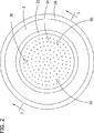
ここで図2を参照すると、それには、内側環状棚22及び複数の孔をもつ多孔表面24を有する改良された受容体2の上面図が示されている。多孔表面24上のウェーハリフト用ピン孔28、30、32により、エピタキシャル蒸着処理の間及び後、改良された受容体2の下にあるリフト用ピン(示せず)は、改良された受容体へ半導体ウェーハを載せたりまた受容体から半導体ウェーハを持ち上げる。改良された受容体2の周辺を囲んでいる縁リング26は、エピタキシャル蒸着処理の間使用され、半導体ウェーハ全体の温度均一性を保証し、温度勾配がウェーハ全体に生じたりまた蒸着処理に悪影響を与えるということがなくなる。縁リング26は、通常、4cmから約10cmの直径であり、改良された受容体2の直径より大きく、高純度のグラファイトから構成され、シリコンカーバイトまたはグラスカーボンコーティングを備えている。
【0018】
本発明の改良された受容体は、受容体の内側環状棚に、任意の直径、例えば、150mm、200mm、300mmのウェーハを収容可能にする大きさと形状にすることができる。改良された受容体は、高純度グラファイトなどの従来からある材料で構成してもよく、高温エピタキシャル蒸着処理の間、グラファイトから周囲環境に放出される不純物の量を減らすため、シリコンカーバイトまたはグラスカーボンの層のコーティングを備えている。受容体を構成するために使用されるグラファイトは、通常少なくとも約99%、さらに好ましくは少なくとも約99.9%、最も好ましくは少なくとも99.99%の純度のグラファイトである。さらに、グラファイトは、鉄、モリブデン、銅、ニッケルなどの金属を合計約20ppm以下で含有しているものが望ましいが、鉄、モリブデン、銅、ニッケルなど金属が合計約5ppm以下で含有するものがより望ましい。グラファイトを被覆するシリコンカーバイトまたはグラスカーボンコーティングは、通常、膜厚約75μmから約150μmであり、約125μmであるものが望ましい。
【0019】
半導体ウェーハの直下に配置された改良された受容体の多孔表面の孔は、シリコンカーバイトまたはグラスカーボンのコーティングが、受容体にドリルで穴を形成した後に該コーティングを受容体に塗布したとき、実質的に孔をブロックすることまたふさぐこともなく、したがってそこを通る流体の流れを制限することもない大きさの径を有することが好ましい。開口(通常は「孔」という)は、四角、溝形、ひし形、もしくはその中を流体が流れることが可能である任意の他の形でも可能でよいことが、当業者に認識されている。開口は、好ましくは約0.1mmから約3mmの幅、より好ましくは約0.1mmから約1mmの幅が、最も好ましくは約0.5mmから約1mmの幅を有する。開口の幅は、開口の2つのコーナ間の最大距離、若しくは開口が円である場合には直径により定義される。孔は改良された受容体に間隔をあけて形成されており、そのために、エピタキシャル蒸着処理のプレベーク工程の間に使用される洗浄ガスが、半導体ウェーハの裏側表面全体に十分に接触してその裏側表面をエッチングする。改良された受容体の孔の間隔は、約0.5mmから約4cm、より好ましくは約2mmから約2cmが、最も好ましくは約6mmから約1.5cmであり、それにより、洗浄ガスは、半導体ウェーハの裏側表面面全体に十分に接触し、裏側表面から実質的に本来の酸化物全てをエッチングすることが可能になる。受容体の表面に対する開口面積合計のパーセンテージは、受容体の全表面積の約0.5%から約4%、さらに好ましくは受容体の全表面積の約1%から3%とする。受容体の表面は、好ましくは1平方センチメートルあたり約0.2孔から0.4孔の密度、より好ましくは1平方センチメートルあたり約0.8孔から約1.75孔である。本明細書内で使用される密度は、均一若しくは不均一な密度を意味する。
【0020】
通常、改良された受容体の孔は、実際には、シリコンカーバイトまたはグラスカーボンのコーティングにより、孔を通り半導体ウェーハの裏側表面への流体の流れが制限されない程度の、小さい直径であるのが望ましい。ドリルにより形成された受容体の孔が大きすぎる場合、裏側表面上に局地的な温度不均一が生じ、それによりウェーハ表側表面上にナノトポロジーの問題が発生する。改良された受容体の大きい直径の孔は、半導体ウェーハの下に配置された加熱ランプによる裏側表面への直接照射によって、半導体ウェーハの裏側表面上に高温部分または低温部分を発生させる。これらの高温または冷低温部分は、半導体ウェーハの表側表面全体に温度勾配を引き起こし、半導体ウェーハの表側表面上のエピタキシャルシリコンの成長を不均一なものにする。エピタキシャル層の不均一な成長は、ウェーハの品質を著しく低下させることになる。改良された受容体上の孔は、受容体に斜めに形成されており、それにより、加熱ランプによる裏側表面への直接照射の可能性はさらに減少し、高温または低温部分の形成によって表側表面上に不均一なエピタキシャルが成長し、さらにそのうえ、改良された受容体上に孔は、ガスが受容体を透過して裏側表面に接触することを可能にし、また外方拡散したドーパント原子が裏側表面から離れ移動することを可能にする。高温または低温部分を形成するポテンシャル、及び孔を介するウェーハへの直接照射による半導体ウェーハ上の温度勾配の発生をさらに減少し、リフト用ピン穴により生じた他の高温または低温部分を減少または無くすため、半導体ウェーハの上下にある加熱ランプのランプ出力比は、ランプから均衡のとれた加熱が行われるように、調整されまた切替られる。
【0021】
本発明の改良された受容体は、エピタキシャル蒸着処理などの化学的蒸着処理装置の一部分として使用してもよい。図3を参照すると、そこには、本発明の改良された受容体36を利用し、エピタキシャル成長処理の際に使用するエピタキシャル反応チャンバ34が示されている。改良された受容体36は回転可能である支持装置58及び59に取り付けられ、エピタキシャル蒸着処理の間、内側環状棚42上に半導体ウェーハ38を支持する大きさと形にされている。半導体ウェーハ38は、改良された受容体36内の多孔面49の孔44、45、46、47、48、49、51と間隔があけられている。リフト用ピン孔62により、改良された受容体36の多孔表面9を介して、リフトピン(図示せず)を半導体ウェーハ38へアクセスし、エピタキシャル蒸着処理の前に、半導体ウェーハ38を、改良された受容体36へ載せ、また蒸着処理後にウェーハを受容体から持ち上げることができる。エピタキシャル蒸着チャンバ34は、更に、エピタキシャル蒸着処理の間の加熱源として、改良された受容体36の上下それぞれに配置された加熱ランプアレイ50及び52を収容している。ガス注入口54及び56は、エピタキシャル蒸着処理のプレベーク工程の間、洗浄ガスの導入を可能にし、洗浄ガスは、半導体ウェーハ38の表側表面60及び裏側表面62にある本来の酸化物の除去を促進するために、半導体ウェーハ38の上下に案内される。エピタキシャル成長工程の間、ガス注入口54は、ウェーハ38上を流れるシリコンを含有するソースガスを導入する。また、ガス注入口56は、半導体ウェーハ38の裏側表面62を洗浄するために水素または不活性ガスをウェーハ38の下に導入し、そして、表側表面から外方拡散した不純物原子を運び去る。図3に示すように、エピタキシャル蒸着チャンバに噴射されたガスは、半導体ウェーハの表側及び裏側表面と平行に流れる。そのような流れパターンは、噴射されたガスを表側表面と接触させるとともに、受容体表面の孔を介して受容体を透過させてウェーハの裏側表面に接触させる。ガスは半導体表面と垂直ではなく平行に流れるため、ウェーハ縁と環状棚縁との間から放出したガスにより半導体ウェーハが環状棚から離脱し変形する可能性は、著しく減少するまたは無くなる。ガス注入口54及び56からチャンバ34内に導入されたガスは、排出口64を通ってチャンバ34から取り除かれる。
【0022】
改良された受容体の孔により、洗浄ガスは改良された受容体を通過し、洗浄工程の間、半導体ウェーハの裏面全体に十分に接触する。その結果、裏側表面にある本来の酸化物は洗浄ガスにより除去される。この本来の酸化物を裏側表面から除去することにより、エピタキシャル層が成長している間、滑らかで連続的なエピタキシャル層が、ソースガスに接触する半導体ウェーハ裏側表面の任意の部分で成長し、裏側表面上で変色むらが生じるのを実質的に防止する。さらに、改良された受容体の孔により、不活性ガスまたは水素がウェーハの裏側表面に接触し、その結果、洗浄工程及びユピタキシャル成長処置の間に、裏側表面から外方拡散するドーパント原子が、半導体ウェーハから排気装置へ運び出され、ウェーハ表側表面のオートドーピングがほとんど無くなる。
【0023】
本発明の受容体を有する上述のエピタキシャル反応チャンバは、エピタキシャル蒸着処理の洗浄工程と成長工程両方に使用してもよい。本発明に係る一つのエピタキシャル蒸着処理では、エピタキシャルシリコン層を、半導体ウェーハの表側表面に成長させる。本発明の好適な実施例では、シリコンウェーハは、大気圧でユピタキシャル蒸着チャンバに導入される。水素または水素と塩酸の混合物などの洗浄ガスは、半導体ウェーハの表側及び裏側表面上にある本来の酸化物層を除去するために、約1,000℃から約1,300℃間の温度で、毎分約1リットルから約50リットルの間の流速で、好ましくは毎分約10リットルから20リットルの間で、少なくとも約10秒間、チャンバへ導入される。
【0024】
本来の酸化物層が半導体ウェーハの表側及び裏側表面から除去されると、洗浄ガスは停止され、反応チャンバの温度は、約600℃から約1,200℃の間に調整される。例えば、シランまたはジクロロシランなどのシリコンを含有するソースガスは、半導体ウェーハの表側表面上に毎分約1リットルから約20リットルの間の流速で、半導体ウェーハ上のエピタキシャルシリコン層が、厚さ約0.1μmから約200μmの間、望ましくは約1μmから約100μmの間で十分に成長するまでの期間中導入される。シリコンを含有するソースガスが、半導体ウェーハの表側表面上の蒸着チャンバに導入されると同時に、窒素またはアルゴンまたは水素またはそれらの混合物、若しくは原料ガスなどのガスが半導体ウェーハの裏側表面の下に、毎分約1リットルから約50リットルの間の流速で、好ましくは毎分約10リットルから約20リットルの間で導入される。その結果、パージガスは、半導体ウェーハの裏側表面に接触し、裏側表面から外方拡散したドーパント原子を排気装置出口へ運び去る。この好適な実施例は、裏側表面の変色むらの影響を著しく減少させまたは排除し、表側表面のオートドーピングを最小限に抑える。好適なエピタキシャル蒸着処理は大気圧で実施されるが、低圧化学蒸着も本発明の範囲内に含まれる。
【0025】
本発明の他の実施例では、改良された受容体は、半導体ウェーハを直に多孔表面に載せることを可能にする大きさと形にしてもよく、その場合、図1に示す内側環状棚22は除かれる。図4は、半導体ウェーハを直に多孔表面に載せている改良された受容体の断面図を示す。半導体ウェーハ70の裏側表面76は、改良された受容体74の多孔表面72上に直に置かれている。ウェーハ70の裏側表面76が直に多孔表面72に接触しているが、改良された受容体74の下を流れるガスは、孔78、80、82、84、86、88、90を介して多孔表面72を透過し、ウェーハ70の裏側表面76全体と十分に接触する。
【0026】
さらに別の実施例では、図4に示す本発明の改良された受容体は更に改良されており、多孔表面72は、半導体ウェーハの外縁のみを改良された受容体に接触させるために、皿状または半球形状に形成されている。ここで、図5には、半導体ウェーハを受容体の多孔表面に直に載せている改良された受容体の断面図が示されている。半導体ウェーハ70の裏側表面76は、改良された受容体74の多孔表面72上に直に置かれている。多孔表面72は、皿または半球形のように形成されており、半導体ウェーハ70の外部縁92及び94が、多孔表面72に直に接触し、ウェーハ70の裏側表面76の残り部分は多孔表面72と直に接触していない。使用中、孔78、80、82、84、86、88、90により、流体はそれを通ってウェーハの裏側表面に流れる。
【0027】
本発明の改良された受容体が、使用される受容体の形状に関係なく、バレル型、パンケーキ型、ミニバッチ型の反応炉を含むさまざまな種類の蒸着反応炉に使用できることは、当業者にとって認識されることである。
【0028】
以上より、本発明の複数の目的は達成されたことがわかる。本発明の範囲から逸脱することなく、上述の改良された受容体を種々改変することができ、本願明細書に含まれる全ての内容は単なる例示であって限定的な意味に解釈されるべきではない。
【図面の簡単な説明】
【図1】 図2の1−1線に沿った面の、本発明である改良された受容体の断面である。
【図2】 本発明に係る改良された受容体の平面図である。
【図3】 図2の1−1線に沿った面で本発明の改良された受容体を示すエピタキシャル反応チャンバの断面である。
【図4】 本発明である改良された受容体の断面である。
【図5】 本発明である改良された受容体の断面である。[0001]
(Background of the Invention)
The present invention relates to an improved receptor for use in chemical vapor deposition. In particular, the present invention relates to an improved receptor having a plurality of holes used in an epitaxial deposition reactor and method, which significantly reduces autodoping of the semiconductor wafer surface and discontinuous silicon growth on the backside of the semiconductor wafer. Or exclude it.
[0002]
In the production of a silicon single crystal grown by the Czochralski method, polycrystalline silicon is first dissolved in a quartz crucible with or without a dopant. After the polycrystalline silicon is melted and the temperature is equilibrated, the seed crystal is placed in the melt, and then the seed crystal is pulled up while rotating the quartz crucible to form a single crystal silicon ingot. . Single crystal silicon ingots are then sliced into individual semiconductor wafers that are subjected to several processes including lapping / grinding, etching, and polishing to produce semiconductor wafers with specular gloss on the surface. The In order to prepare a wafer for device fabrication, the wafer is subjected to a chemical vapor deposition process such as an epitaxial deposition process. In this deposition process, a thin silicon layer, typically about 0.1 to about 200 μm thick, is grown on the surface of the wafer, which allows the device to be assembled directly on the epitaxial layer. Conventional epitaxial deposition processes are disclosed in US Pat. Nos. 5,904,769 and 5,769,942.
[0003]
The epitaxial deposition process is generally composed of two steps. In the first step, after the semiconductor wafer is placed in the deposition chamber and lowered onto the receptor, the front surface of the wafer is pre-baked by exposure to a cleaning gas such as hydrogen or a hydrogen / hydrochloric acid mixture at about 1150 ° C. The By cleaning the surface of the semiconductor wafer to remove the original oxide on the surface, a flat and continuous epitaxial silicon layer can be grown on the front surface. In the second step of the epitaxial deposition process, the front surface of the wafer is exposed to a source of vaporous silicon (eg, silane or trichlorosilane) at about 800 ° C. or higher to deposit an epitaxial silicon layer on the front surface. To be grown. During both steps of the epitaxial deposition process, the semiconductor wafer is supported in the epitaxial deposition chamber by a receptor that is rotated to achieve uniform growth of the epitaxial layer. The receptor is usually composed of high purity graphite and has a silicon carbide layer that completely covers the graphite to reduce the amount of iron and other contaminants released from the graphite during high temperature processing. . Conventional receptors used in epitaxial growth processes are well known in the art and are disclosed in US Pat. Nos. 4,322,592, 4,496,609, 5,200,157, and 5,242,501.
[0004]
When using a conventional receptor for epitaxial deposition processes, during the loading process to lower the wafer to the receiver, gas is trapped between the receiver and the wafer, and the wafer floats and slides on the receiver. It will be tilted. This makes the epitaxial growth non-uniform. In addition, during the pre-bake process, a small amount of cleaning gas, such as hydrogen, is released around the wafer edge between the wafer and the receiver and enters the space between the wafer and the receiver. When the backside surface of the wafer is sealed with an oxide layer (low temperature oxide layer), the released hydrogen does not react well with the oxide layer and forms pinholes in the layer or the oxide layer Cannot be completely removed. If the backside surface is an etched or polishing surface required by many equipment manufacturers, if the cleaning gas is only a thin original oxide layer released around the wafer, near the outer edge of the wafer backside surface The oxide layer is completely removed by hydrogen or a hydrogen / chlorine acid mixture to form pinhole openings in the oxide layer so that the silicon surface is exposed as the etching process moves away from the outer edge of the wafer. Will do. These pinhole openings typically form rings or discoloration irregularities around the wafer.
[0005]
During the epitaxial deposition process, a small amount of silicon-containing source gas is released to the wafer edge between the wafer and the receptor and enters the space between the wafer and the receptor. When the backside surface of the wafer is sealed with oxide, crystal nucleation and silicon film growth are significantly suppressed. In the portion where the original oxide layer is completely etched by the cleaning gas, a smooth and continuous silicon layer grows. However, if the cleaning gas has not completely removed the original oxide layer, the silicon-containing source gas deposits silicon into the pinhole, and during epitaxial deposition, a non-uniform thin silicon layer is formed on the wafer backside surface. Form. Therefore, in a wafer having an etched or polished backside surface that has only the native oxide layer, pinholes formed in the native oxide layer during the pre-bake process cause discontinuous silicon on the wafer backside surface. Growth occurs and it appears cloudy when exposed to bright light. This haze or discoloration unevenness on the backside surface of the wafer consists of small silicon growths or ridges with a diameter of about 0.5 μm and a height of about 10 nm. These ridges of silicon disperse the light and cause fogging, interfering with machine observation and optical pyrometry devices to interfere with machine vision and optical pyrometer systems that observe the wafer backside surface during device processing. Because it is undesirable.
[0006]
Another problem encountered during the growth of epitaxial silicon layers at high temperatures is the outdiffusion of dopant atoms such as boron and phosphorus through the backside surface of the semiconductor wafer during the high temperature prebake and epitaxial growth processes. . In conventional receptors, dopant atoms that have diffused out of the backside surface are confined between the receptor and the wafer itself, and are emitted from between the receptor and the wafer edge toward the frontside surface of the wafer. These dopant atoms enter the growing deposition layer and become contaminated, reducing the resistivity uniformity near the wafer edge. If the backside surface of the semiconductor wafer is sealed with, for example, a low temperature oxide, the dopant atoms will not substantially diffuse outward from the backside surface. However, in a semiconductor wafer having an etched or polished backside surface, out-diffusion of dopant atoms from the backside surface occurs during the epitaxial deposition process, thereby causing undesired frontside surface autodoping.
[0007]
Several methods have been proposed as an attempt to eliminate uneven color change and autodoping on the backside surface. In order to eliminate discoloration unevenness on the backside surface, Nakamura (Japanese Patent Publication No. 11-16844) discloses performing hydrogen fluoride cleaning and / or high-temperature hydrogen annealing treatment on the backside surface of the wafer. Yes. By 10 days prior to loading the wafer into the epitaxial reactor, the process adds additional processing steps that can greatly complicate and increase the cost of the deposition process. Deaton et al. (US Pat. No. 5,960,555) use a receptor with channels along the edge of the wafer to direct the flow of purge gas to the edge of the wafer, thereby bringing the reaction source gas on the front side to the back side of the wafer. A method for preventing divergence is disclosed. This method requires significant modifications to existing epitaxial deposition chambers. In addition, since this method uses a large amount of purge gas, the purge gas leaks to the front surface of the wafer and mixes with the source gas, which degrades the quality of the epitaxial film that is completed.
[0008]
In order to reduce autodoping, Hoshi (Japanese Patent Publication No. 11-87250) discloses that vacuum doping at the edge of the receptor removes boron dopant at the edge of the receptor to prevent autodoping. ing. This method affects the uniformity and thickness of the wafer edge and requires considerable modifications to existing epitaxial deposition systems. Nakamura (Japanese Patent Publication No. 10-223545) discloses an improved receptor having a plurality of slots at the edges of the receptor, in which out-diffused dopant atoms are exhausted through the slots. To extrude. This method also causes a large amount of vapor deposition gas to be exhausted under the backside surface of the wafer, which can cause premature corrosion and safety problems of the exhaust system as well as the effects of the aforementioned discoloration unevenness.
[0009]
To date, no satisfactory method has been proposed to eliminate the uneven discoloration and autodoping problems that occur on the backside surface of semiconductors associated with the outward diffusion of dopants from the backside surface of the wafer during the epitaxial deposition process. . Thus, there is a need in the semiconductor industry for a simple and cost effective strategy that resolves, for example, the effects of uneven discoloration and undesirable autodoping of the semiconductor front side surface that occurs during epitaxial deposition processes.
[0010]
(Summary of the Invention)
With the improved receptor supply within the purpose of the present invention, the cleaning gas is in full contact with the entire backside surface of the semiconductor wafer. By providing an improved receptor, the autodoping of the front surface of the semiconductor wafer is significantly reduced during epitaxial silicon growth. By providing an improved receptor, the removal of the native oxide from the backside surface of the semiconductor wafer is sufficiently completed during the pre-bake process of epitaxial deposition, and the effect of uneven discoloration is virtually eliminated. By providing an improved receptor having a plurality of holes, the quality of an epitaxial wafer produced using the receptor is improved. By providing an improved receptor, the floating state of the wafer is reduced or eliminated during loading.
[0011]
Briefly, the present invention is directed to an apparatus for performing a chemical vapor deposition process for growing an epitaxial layer on a semiconductor wafer. The apparatus has a receiver sized and shaped to support a semiconductor wafer. The receiver has a surface with an aperture density having apertures at a rate of about 0.2 to about 4 per square centimeter, with fluid flowing through the apertures, usually by a surface parallel and facing the wafer. .
[0012]
The present invention is further directed to an apparatus for performing an epitaxial deposition process for growing an epitaxial layer on a semiconductor wafer. The apparatus has a receiver sized and shaped to support a semiconductor wafer. The receiver has a surface with an aperture density having apertures at a rate of about 0.5 to about 2 per square centimeter, and the fluid usually flows through the apertures by a surface that is parallel and opposite to the wafer. . The apparatus further comprises a rotating device that supports the receiver and wafer, a heating element, an edge ring surrounding the receiver, and a gas inlet and a gas outlet.
[0013]
The present invention is further directed to a process for growing an epitaxial silicon layer on a semiconductor wafer. In this process, a cleaning gas is introduced into the epitaxial deposition chamber containing the wafer to remove the native oxide layer from the surface, flows parallel to the front and back surfaces, contacts the front surface of the wafer, It also makes good contact with the backside surface. A source gas containing silicon next to the cleaning gas is introduced into the deposition chamber to grow an epitaxial silicon layer on the front surface.
[0014]
Other objects and features of the invention will be in part apparent and will in part be pointed out hereinafter.
[0015]
Detailed Description of the Preferred Embodiment
According to the present invention, a high quality semiconductor wafer having an epitaxial silicon layer on the front side surface is obtained by utilizing an epitaxial deposition chamber incorporating an improved receptor having a plurality of openings. Conveniently, the improved receiver substantially eliminates “floating” during loading and allows fluid transport toward or from the wafer backside surface. Therefore, the cleaning gas used in the pre-bake process of the epitaxial deposition process contacts almost the entire surface of the back side of the semiconductor wafer and chemically removes almost all the original oxide layer. As a result, during the growth of the epitaxial layer, when the source gas contacts the backside surface of the semiconductor wafer, a smooth and continuous silicon layer grows, and the discoloration unevenness on the backside surface of the wafer is reduced or eliminated. Also, according to the improved receptor, dopant atoms contained in the semiconductor wafer, which diffuse out from the wafer backside surface during the epitaxial deposition process, are moved away from the front surface of the wafer by the purge gas flow. Since it is sent to the exhaust portion, a large amount of dopant is discharged from between the wafer and the edge of the receiver and does not cause undesirable autodoping on the front surface of the wafer due to contact with the front surface of the wafer.
[0016]
Referring to the figures, and in particular, FIG. 1 shows a cross-sectional view of an
[0017]
Reference is now made to FIG. 2, which shows a top view of an
[0018]
The improved receptor of the present invention can be sized and shaped to accommodate wafers of any diameter, eg 150 mm, 200 mm, 300 mm, on the inner annular shelf of the receiver. The improved receptor may be composed of conventional materials such as high purity graphite, and silicon carbide or glass to reduce the amount of impurities released from the graphite to the ambient environment during the high temperature epitaxial deposition process. With carbon layer coating. The graphite used to make up the receptor is usually graphite with a purity of at least about 99%, more preferably at least about 99.9%, and most preferably at least 99.99%. Further, graphite preferably contains metals such as iron, molybdenum, copper and nickel at a total of about 20 ppm or less, but more preferably contains metals such as iron, molybdenum, copper and nickel at a total of about 5 ppm or less. desirable. The silicon carbide or glass carbon coating that coats the graphite typically has a film thickness of about 75 μm to about 150 μm, preferably about 125 μm.
[0019]
The hole on the porous surface of the improved receptor located directly under the semiconductor wafer is when the coating of silicon carbide or glass carbon is applied to the receptor after the hole has been drilled into the receptor, It is preferred to have a diameter that does not substantially block or block the hole and therefore does not restrict the flow of fluid therethrough. It will be appreciated by those skilled in the art that the openings (usually referred to as “holes”) can be square, grooved, diamond shaped, or any other shape through which fluid can flow. The opening preferably has a width of about 0.1 mm to about 3 mm, more preferably a width of about 0.1 mm to about 1 mm, and most preferably a width of about 0.5 mm to about 1 mm. The width of the opening is defined by the maximum distance between the two corners of the opening, or the diameter if the opening is a circle. The pores are spaced apart in the improved receptor, so that the cleaning gas used during the pre-baking step of the epitaxial deposition process is sufficiently in contact with the entire backside surface of the semiconductor wafer. Etch the surface. The improved receptor pore spacing is from about 0.5 mm to about 4 cm, more preferably from about 2 mm to about 2 cm, and most preferably from about 6 mm to about 1.5 cm, so that the cleaning gas is a semiconducting gas. The entire backside surface of the wafer is in full contact and allows substantially all of the native oxide to be etched from the backside surface. The percentage of the total open area relative to the surface of the receptor is about 0.5% to about 4% of the total surface area of the receptor, more preferably about 1% to 3% of the total surface area of the receptor. The surface of the receptor preferably has a density of about 0.2 to 0.4 holes per square centimeter, more preferably about 0.8 to about 1.75 holes per square centimeter. As used herein, density means uniform or non-uniform density.
[0020]
Typically, the improved receptor holes are actually small in diameter so that the silicon carbide or glass carbon coating does not restrict fluid flow through the holes to the backside surface of the semiconductor wafer. desirable. If the hole in the receptor formed by the drill is too large, a local temperature non-uniformity occurs on the backside surface, thereby creating nanotopology problems on the wafer frontside surface. The improved receptor large diameter holes generate hot or cold portions on the backside surface of the semiconductor wafer by direct illumination of the backside surface by a heating lamp located under the semiconductor wafer. These hot or cold portions cause a temperature gradient across the front surface of the semiconductor wafer, causing uneven growth of epitaxial silicon on the front surface of the semiconductor wafer. Non-uniform growth of the epitaxial layer will significantly degrade the quality of the wafer. The holes on the improved receptor are diagonally formed in the receptor, thereby further reducing the possibility of direct irradiation of the backside surface by a heating lamp and on the front surface by the formation of hot or cold parts. In addition, heterogeneous epitaxial growth occurs on the surface of the improved receptor, as well as holes that allow gas to permeate the receptor and contact the backside surface, and out-diffusion dopant atoms are present on the backside surface. Allows you to move away from. To further reduce the potential to form hot or cold parts and the generation of temperature gradients on the semiconductor wafer by direct irradiation of the wafer through the holes, and to reduce or eliminate other hot or cold parts caused by the lift pin holes The lamp power ratios of the heating lamps above and below the semiconductor wafer are adjusted and switched so that balanced heating is performed from the lamps.
[0021]
The improved receptor of the present invention may be used as part of a chemical vapor deposition apparatus such as an epitaxial vapor deposition process. Referring to FIG. 3, there is shown an
[0022]
The improved receptor holes allow the cleaning gas to pass through the improved receiver and fully contact the entire backside of the semiconductor wafer during the cleaning process. As a result, the original oxide on the back surface is removed by the cleaning gas. By removing this native oxide from the backside surface, a smooth and continuous epitaxial layer grows on any part of the backside surface of the semiconductor wafer that contacts the source gas while the epitaxial layer is growing, and the backside Substantially prevent the occurrence of uneven discoloration on the surface. In addition, the improved acceptor pores allow inert gas or hydrogen to contact the backside surface of the wafer, so that dopant atoms that diffuse out of the backside surface during the cleaning process and the epitaxial growth procedure, It is carried from the semiconductor wafer to the exhaust device, and there is almost no auto-doping on the front surface of the wafer.
[0023]
The above-described epitaxial reaction chamber having the receptor of the present invention may be used for both the cleaning process and the growth process of the epitaxial deposition process. In one epitaxial deposition process according to the present invention, an epitaxial silicon layer is grown on the front surface of a semiconductor wafer. In the preferred embodiment of the present invention, the silicon wafer is introduced into the optical deposition chamber at atmospheric pressure. A cleaning gas, such as hydrogen or a mixture of hydrogen and hydrochloric acid, at a temperature between about 1,000 ° C. and about 1,300 ° C. to remove the native oxide layers on the front and back surfaces of the semiconductor wafer, The chamber is introduced into the chamber at a flow rate between about 1 liter and about 50 liters per minute, preferably between about 10 liters and 20 liters per minute for at least about 10 seconds.
[0024]
When the native oxide layer is removed from the front and back surfaces of the semiconductor wafer, the cleaning gas is turned off and the temperature of the reaction chamber is adjusted to between about 600 ° C and about 1200 ° C. For example, a source gas containing silicon, such as silane or dichlorosilane, has a flow rate between about 1 liter to about 20 liters per minute on the front surface of the semiconductor wafer, and the epitaxial silicon layer on the semiconductor wafer has a thickness of about It is introduced during a period until it grows sufficiently between 0.1 μm and about 200 μm, desirably between about 1 μm and about 100 μm. While a source gas containing silicon is introduced into the deposition chamber on the front surface of the semiconductor wafer, a gas such as nitrogen or argon or hydrogen or a mixture thereof, or a source gas is under the back surface of the semiconductor wafer, It is introduced at a flow rate between about 1 liter and about 50 liters per minute, preferably between about 10 liters and about 20 liters per minute. As a result, the purge gas contacts the backside surface of the semiconductor wafer and carries away dopant atoms diffused outward from the backside surface to the exhaust device outlet. This preferred embodiment significantly reduces or eliminates the effect of uneven discoloration on the back surface and minimizes autodoping on the front surface. A suitable epitaxial deposition process is performed at atmospheric pressure, although low pressure chemical vapor deposition is within the scope of the present invention.
[0025]
In other embodiments of the invention, the improved receiver may be sized and shaped to allow a semiconductor wafer to be placed directly on the porous surface, in which case the inner
[0026]
In yet another embodiment, the improved receiver of the present invention shown in FIG. 4 is further improved, and the
[0027]
It will be appreciated by those skilled in the art that the improved receptor of the present invention can be used in various types of vapor deposition reactors, including barrel type, pancake type, mini-batch type reactors, regardless of the receiver shape used. It is to be recognized.
[0028]
From the above, it can be seen that a plurality of objects of the present invention have been achieved. Various modifications can be made to the improved receptor described above without departing from the scope of the present invention, and all contents contained herein are merely exemplary and should not be construed in a limiting sense. Absent.
[Brief description of the drawings]
FIG. 1 is a cross-section of an improved receptor of the present invention, taken along the line 1-1 in FIG.
FIG. 2 is a plan view of an improved receptor according to the present invention.
FIG. 3 is a cross section of an epitaxial reaction chamber showing the improved receptor of the present invention in the plane along line 1-1 of FIG.
FIG. 4 is a cross section of the improved receptor of the present invention.
FIG. 5 is a cross section of the improved receptor of the present invention.
Claims (17)
この受容体は、
上記受容体に支持された半導体ウェーハの裏側表面にほぼ平行に対向し、上記受容体を介して上記半導体ウェーハの裏側表面にガスの流れを接触させる多孔面を有し、
上記多孔面は1平方センチメートルあたり0.2個から4個の割合で開口部を有する開口密度を備えており、
上記多孔面における全開口領域の割合が0.5%と4%の間であり、
上記受容体は、上記受容体の周囲を囲む縁リングを備えている受容体。A receptor for supporting a semiconductor wafer during chemical vapor deposition for growing an epitaxial silicon layer on a semiconductor wafer having a front surface and a back surface,
This receptor is
Opposite parallel to the back side surface of the semiconductor wafer supported by the receptor, and having a porous surface for contacting the flow of gas to the back side surface of the semiconductor wafer through the receptor,
The porous surface has an opening density having openings of 0.2 to 4 per square centimeter;
The percentage of the total open area in the perforated surface Ri der between 0.5% and 4%,
The receptor comprising an edge ring surrounding the periphery of the receptor.
上記チャンバの内部空間内で半導体ウェーハを支持する大きさと形状を有し、
上記多孔面が、上記半導体が支持されている間、上記多孔面を介してガスを内側に向けて流して上記半導体ウェーハの裏側表面に接触させるとともに上記多孔面を介してガスを外側に流して上記ガス出口を通じて上記チャンバから排出するように上記チャンバ内に露出されている請求項1の受容体。Used with a chamber comprising an internal space, a gas inlet for introducing gas into the internal space in the chamber, and a gas outlet for exhausting the gas from the internal space of the chamber;
Having a size and shape for supporting a semiconductor wafer in the internal space of the chamber;
While the semiconductor is supported by the porous surface, the gas flows inward through the porous surface to contact the back side surface of the semiconductor wafer, and the gas flows outward through the porous surface. receptor of claim 1 which is exposed to the chamber so as to discharge from said chamber through said gas outlet.
上記チャンバの中で受容体を支持する受容体支持部であって、上記受容体の第2の側が上記チャンバの内部に露出して上記受容体の多孔面を介して上記ガスを内側に自由に流して上記半導体ウェーハの裏側表面に接触させるとともに上記受容体の多孔面を介して上記ガスを外側に流して上記ガス出口を通じて上記チャンバから排出するものとともに使用される請求項1に記載の受容体。A vapor deposition chamber for forming an internal space having a gas inlet for introducing gas into the internal space of the chamber and a gas outlet for discharging gas from the internal space of the chamber;
A receptor support for supporting a receptor in the chamber, wherein the second side of the receptor is exposed to the inside of the chamber so that the gas can freely pass inward through the porous surface of the receptor; The receptor according to claim 1 , wherein the receptor is used together with a gas flowing into contact with the backside surface of the semiconductor wafer and flowing out of the gas through the porous surface of the receptor and discharged from the chamber through the gas outlet. .
チャンバの内部空間に配置された受容体にウェーハを載せる積載工程であって、上記受容体は該受容体の第1の側から第2の側へ伸びる複数の開口部を備えた多孔部を有し、上記積載工程は上記ウェーハの裏側表面が上記受容体の多孔部の第1の側に対向するように上記ウェーハを上記受容体に乗せることを含む工程と、
上記受容体の第2の側が上記チャンバの内部空間に露出するように上記チャンバの内部に上記受容体を支持する工程と、
上記チャンバの内部空間にガスを流し、上記受容体の多孔面を介して上記ガスの自由な流れを内側に向けて上記半導体の裏側表面に接触させて上記裏側表面を処理するとともに上記受容体の多孔面を介して上記ガスの流れを外側に向けて上記チャンバの内部空間に戻す工程と、
上記チャンバの内部空間からガスを排出する工程と、
上記チャンバの内部空間で上記受容体を回転し、その間、上記ガスが上記チャンバの内部空間に向けて流される工程を有する方法。A method of treating the back side surface of a semiconductor wafer having a front side surface and a back side surface with a gas,
A loading step of placing a wafer on a receptor disposed in an interior space of the chamber, wherein the receptor has a porous portion having a plurality of openings extending from a first side to a second side of the receptor; The loading step includes placing the wafer on the receiver such that the back side surface of the wafer faces the first side of the porous portion of the receptor;
Supporting the receptor within the chamber such that a second side of the receptor is exposed to the interior space of the chamber;
A gas is flowed into the internal space of the chamber, the free surface flow of the gas is directed inward through the porous surface of the receptor, and the back surface of the semiconductor is treated by contacting the back surface of the semiconductor. Returning the gas flow to the outside through the porous surface and returning to the internal space of the chamber;
Exhausting gas from the interior space of the chamber;
Rotating the receptor in the interior space of the chamber, during which time the gas is flowed towards the interior space of the chamber.
上記半導体ウェーハを収容するチャンバの内部空間にクリーニングガスを導入する工程であって、上記クリーニングガスが上記表側表面と裏側表面に平行に流れ、上記半導体ウェーハの表側表面に接触するとともに上記半導体ウェーハの裏側表面の全体に接触して、上記半導体ウェーハの表側表面と裏側表面からもともとの酸化物層を除去する工程と、
シリコン含有のソースガスをチャンバの内部空間に導入して上記半導体ウェーハの表側表面にエピタキシャルシリコン層を成長させるとともに、チャンバの内部空間にパージガスを導入して上記半導体ウェーハの裏側表面から外方拡散したドーパント原子を上記半導体ウェーハの表側表面から取り除く工程とを含む請求項15に記載の方法。The process of flowing gas into the interior space of the chamber
Introducing a cleaning gas into the internal space of the chamber containing the semiconductor wafer, the cleaning gas flowing in parallel to the front surface and the back surface, contacting the front surface of the semiconductor wafer and the semiconductor wafer; Contacting the entire back side surface, removing the original oxide layer from the front side surface and back side surface of the semiconductor wafer;
A silicon-containing source gas is introduced into the internal space of the chamber to grow an epitaxial silicon layer on the front surface of the semiconductor wafer, and a purge gas is introduced into the internal space of the chamber to diffuse outward from the back surface of the semiconductor wafer. the method of claim 15, the dopant atoms and a step of removing from the front surface of the semiconductor wafer.
Applications Claiming Priority (2)
| Application Number | Priority Date | Filing Date | Title |
|---|---|---|---|
| US09/566,890 US6444027B1 (en) | 2000-05-08 | 2000-05-08 | Modified susceptor for use in chemical vapor deposition process |
| PCT/US2001/012668 WO2001086034A2 (en) | 2000-05-08 | 2001-04-19 | Modified susceptor for use in chemical vapor deposition process |
Publications (3)
| Publication Number | Publication Date |
|---|---|
| JP2004522294A JP2004522294A (en) | 2004-07-22 |
| JP2004522294A5 JP2004522294A5 (en) | 2006-01-05 |
| JP4492840B2 true JP4492840B2 (en) | 2010-06-30 |
Family
ID=24264828
Family Applications (1)
| Application Number | Title | Priority Date | Filing Date |
|---|---|---|---|
| JP2001582617A Expired - Lifetime JP4492840B2 (en) | 2000-05-08 | 2001-04-19 | Improved receptor for use in chemical vapor deposition processes. |
Country Status (8)
| Country | Link |
|---|---|
| US (3) | US6444027B1 (en) |
| EP (1) | EP1287187B1 (en) |
| JP (1) | JP4492840B2 (en) |
| KR (1) | KR100784001B1 (en) |
| CN (1) | CN1223709C (en) |
| DE (1) | DE60139008D1 (en) |
| TW (1) | TWI285936B (en) |
| WO (1) | WO2001086034A2 (en) |
Families Citing this family (119)
| Publication number | Priority date | Publication date | Assignee | Title |
|---|---|---|---|---|
| US6113702A (en) * | 1995-09-01 | 2000-09-05 | Asm America, Inc. | Wafer support system |
| US6183565B1 (en) * | 1997-07-08 | 2001-02-06 | Asm International N.V | Method and apparatus for supporting a semiconductor wafer during processing |
| US6444027B1 (en) * | 2000-05-08 | 2002-09-03 | Memc Electronic Materials, Inc. | Modified susceptor for use in chemical vapor deposition process |
| DE10027931C1 (en) * | 2000-05-31 | 2002-01-10 | Infineon Technologies Ag | Method for rear-side electrical contacting of a semiconductor substrate during its processing |
| US6599815B1 (en) * | 2000-06-30 | 2003-07-29 | Memc Electronic Materials, Inc. | Method and apparatus for forming a silicon wafer with a denuded zone |
| US6822945B2 (en) | 2000-11-08 | 2004-11-23 | Genesys Telecommunications Laboratories, Inc. | Method and apparatus for anticipating and planning communication-center resources based on evaluation of events waiting in a communication center master queue |
| US6576572B2 (en) * | 2000-12-28 | 2003-06-10 | Schott Lithotec Ag | Method of heating a substrate using a variable surface hot plate for improved bake uniformity |
| DE10111761A1 (en) * | 2001-03-12 | 2002-10-02 | Infineon Technologies Ag | Arrangement and method for contacting a semiconductor substrate from the rear |
| JP2003229370A (en) * | 2001-11-30 | 2003-08-15 | Shin Etsu Handotai Co Ltd | Susceptor, vapor phase growth device, method of manufacturing epitaxial wafer, and epitaxial wafer |
| WO2003046966A1 (en) * | 2001-11-30 | 2003-06-05 | Shin-Etsu Handotai Co., Ltd. | Susceptor, gaseous phase growing device, device and method for manufacturing epitaxial wafer, and epitaxial wafer |
| JP4061062B2 (en) * | 2001-12-13 | 2008-03-12 | ローム株式会社 | Semiconductor light emitting device manufacturing method and oxidation furnace |
| US20050000449A1 (en) * | 2001-12-21 | 2005-01-06 | Masayuki Ishibashi | Susceptor for epitaxial growth and epitaxial growth method |
| JP2003197532A (en) * | 2001-12-21 | 2003-07-11 | Sumitomo Mitsubishi Silicon Corp | Epitaxial growth method and epitaxial growth suscepter |
| DE10211312A1 (en) | 2002-03-14 | 2003-10-02 | Wacker Siltronic Halbleitermat | Epitaxial coating applying method of semiconductor wafer in chemical vapor deposition reactor, involves exposing back surface of semiconductor wafer to ejection gas containing specific amount of hydrogen |
| JP4089354B2 (en) * | 2002-08-30 | 2008-05-28 | 株式会社Sumco | Epitaxial wafer and manufacturing method thereof |
| JP4016823B2 (en) * | 2002-12-06 | 2007-12-05 | 信越半導体株式会社 | Manufacturing method of silicon epitaxial wafer |
| DE10261362B8 (en) * | 2002-12-30 | 2008-08-28 | Osram Opto Semiconductors Gmbh | Substrate holder |
| US20060225642A1 (en) * | 2003-03-31 | 2006-10-12 | Yoshihiko Kanzawa | Method of forming semiconductor crystal |
| US7064073B1 (en) * | 2003-05-09 | 2006-06-20 | Newport Fab, Llc | Technique for reducing contaminants in fabrication of semiconductor wafers |
| JP4066881B2 (en) * | 2003-05-21 | 2008-03-26 | 信越半導体株式会社 | Surface treatment method, silicon epitaxial wafer manufacturing method, and silicon epitaxial wafer |
| DE102004060625A1 (en) * | 2004-12-16 | 2006-06-29 | Siltronic Ag | Coated semiconductor wafer and method and apparatus for producing the semiconductor wafer |
| US7285483B2 (en) * | 2003-06-26 | 2007-10-23 | Silitronic Ag | Coated semiconductor wafer, and process and apparatus for producing the semiconductor wafer |
| DE10328842B4 (en) * | 2003-06-26 | 2007-03-01 | Siltronic Ag | A chemical vapor deposition susceptor, a process for processing a semiconductor wafer by chemical vapor deposition, and a process wafer |
| JP4839836B2 (en) * | 2003-06-26 | 2011-12-21 | 信越半導体株式会社 | Manufacturing method of silicon epitaxial wafer |
| JP4655935B2 (en) * | 2003-10-01 | 2011-03-23 | 信越半導体株式会社 | Manufacturing method of silicon epitaxial wafer |
| US7827930B2 (en) * | 2004-01-26 | 2010-11-09 | Applied Materials, Inc. | Apparatus for electroless deposition of metals onto semiconductor substrates |
| US7323058B2 (en) * | 2004-01-26 | 2008-01-29 | Applied Materials, Inc. | Apparatus for electroless deposition of metals onto semiconductor substrates |
| US7654221B2 (en) * | 2003-10-06 | 2010-02-02 | Applied Materials, Inc. | Apparatus for electroless deposition of metals onto semiconductor substrates |
| US7166528B2 (en) * | 2003-10-10 | 2007-01-23 | Applied Materials, Inc. | Methods of selective deposition of heavily doped epitaxial SiGe |
| US7235139B2 (en) * | 2003-10-28 | 2007-06-26 | Veeco Instruments Inc. | Wafer carrier for growing GaN wafers |
| DE10357698A1 (en) * | 2003-12-09 | 2005-07-14 | Schunk Kohlenstofftechnik Gmbh | Carrier for objects to be treated and method for producing such |
| KR101112029B1 (en) * | 2004-02-13 | 2012-03-21 | 에이에스엠 아메리카, 인코포레이티드 | Substrate Support System for Reduced Autodoping and Backside Deposition |
| US20050193951A1 (en) * | 2004-03-08 | 2005-09-08 | Muneo Furuse | Plasma processing apparatus |
| JP4636807B2 (en) * | 2004-03-18 | 2011-02-23 | キヤノン株式会社 | Substrate holding device and exposure apparatus using the same |
| US20080032040A1 (en) * | 2004-03-29 | 2008-02-07 | Akira Okabe | Wafer Support and Semiconductor Substrate Processing Method |
| US20050217585A1 (en) * | 2004-04-01 | 2005-10-06 | Blomiley Eric R | Substrate susceptor for receiving a substrate to be deposited upon |
| US20050217569A1 (en) * | 2004-04-01 | 2005-10-06 | Nirmal Ramaswamy | Methods of depositing an elemental silicon-comprising material over a semiconductor substrate and methods of cleaning an internal wall of a chamber |
| US20050223985A1 (en) * | 2004-04-08 | 2005-10-13 | Blomiley Eric R | Deposition apparatuses, methods of assessing the temperature of semiconductor wafer substrates within deposition apparatuses, and methods for deposition of epitaxial semiconductive material |
| US20050223993A1 (en) * | 2004-04-08 | 2005-10-13 | Blomiley Eric R | Deposition apparatuses; methods for assessing alignments of substrates within deposition apparatuses; and methods for assessing thicknesses of deposited layers within deposition apparatuses |
| JP2005333090A (en) * | 2004-05-21 | 2005-12-02 | Sumco Corp | P-type silicon wafer and method for heat-treatment thereof |
| JP2006040972A (en) * | 2004-07-22 | 2006-02-09 | Shin Etsu Handotai Co Ltd | Silicon epitaxial wafer and its manufacturing method |
| JP4304720B2 (en) * | 2004-07-30 | 2009-07-29 | 信越半導体株式会社 | Susceptor, vapor phase growth apparatus, epitaxial wafer manufacturing method, and epitaxial wafer |
| US7250358B2 (en) * | 2004-08-06 | 2007-07-31 | Globitech Incorporated | Wafer for preventing the formation of silicon nodules and method for preventing the formation of silicon nodules |
| KR100678468B1 (en) * | 2005-01-14 | 2007-02-02 | 삼성전자주식회사 | Method for in-situ cleaning semiconductor substrate and method of fabricating semiconductor device employing the same |
| US7198677B2 (en) * | 2005-03-09 | 2007-04-03 | Wafermasters, Inc. | Low temperature wafer backside cleaning |
| US7462246B2 (en) * | 2005-04-15 | 2008-12-09 | Memc Electronic Materials, Inc. | Modified susceptor for barrel reactor |
| US7474114B2 (en) * | 2005-09-08 | 2009-01-06 | Sitronic Corporation | System and method for characterizing silicon wafers |
| KR100794719B1 (en) * | 2005-11-02 | 2008-01-15 | 주식회사 실트론 | Susceptor for chemical vapor-phase deposition apparatus |
| US7485928B2 (en) * | 2005-11-09 | 2009-02-03 | Memc Electronic Materials, Inc. | Arsenic and phosphorus doped silicon wafer substrates having intrinsic gettering |
| TWI354320B (en) * | 2006-02-21 | 2011-12-11 | Nuflare Technology Inc | Vopor phase deposition apparatus and support table |
| US7566951B2 (en) | 2006-04-21 | 2009-07-28 | Memc Electronic Materials, Inc. | Silicon structures with improved resistance to radiation events |
| US20070282471A1 (en) * | 2006-06-01 | 2007-12-06 | Integrated System Solution Corp. | Bluetooth audio chip with multiple input/output sources |
| CN100392815C (en) * | 2006-06-02 | 2008-06-04 | 河北工业大学 | Apparatus capable of eliminating slip line and high stress zone in silicon gas phase epitaxial layer |
| US8951351B2 (en) * | 2006-09-15 | 2015-02-10 | Applied Materials, Inc. | Wafer processing hardware for epitaxial deposition with reduced backside deposition and defects |
| US8852349B2 (en) * | 2006-09-15 | 2014-10-07 | Applied Materials, Inc. | Wafer processing hardware for epitaxial deposition with reduced auto-doping and backside defects |
| DE102006055038B4 (en) * | 2006-11-22 | 2012-12-27 | Siltronic Ag | An epitaxated semiconductor wafer and apparatus and method for producing an epitaxied semiconductor wafer |
| CN101241854B (en) * | 2007-02-06 | 2011-06-01 | 中芯国际集成电路制造(上海)有限公司 | A wafer production technology |
| US8083963B2 (en) * | 2007-02-08 | 2011-12-27 | Applied Materials, Inc. | Removal of process residues on the backside of a substrate |
| US7605054B2 (en) * | 2007-04-18 | 2009-10-20 | S.O.I.Tec Silicon On Insulator Technologies | Method of forming a device wafer with recyclable support |
| US20080314319A1 (en) * | 2007-06-19 | 2008-12-25 | Memc Electronic Materials, Inc. | Susceptor for improving throughput and reducing wafer damage |
| DE102008010041A1 (en) * | 2007-09-28 | 2009-04-02 | Osram Opto Semiconductors Gmbh | Layer deposition apparatus, e.g. for epitaxial deposition of compound semiconductor layers, has segmented process gas enclosure in which substrate is moved relative to partition |
| US20090165721A1 (en) * | 2007-12-27 | 2009-07-02 | Memc Electronic Materials, Inc. | Susceptor with Support Bosses |
| US8404049B2 (en) * | 2007-12-27 | 2013-03-26 | Memc Electronic Materials, Inc. | Epitaxial barrel susceptor having improved thickness uniformity |
| JP5396737B2 (en) * | 2008-04-04 | 2014-01-22 | 株式会社Sumco | Epitaxial silicon wafer and manufacturing method thereof |
| US20090280248A1 (en) * | 2008-05-06 | 2009-11-12 | Asm America, Inc. | Porous substrate holder with thinned portions |
| DE102008023054B4 (en) * | 2008-05-09 | 2011-12-22 | Siltronic Ag | Process for producing an epitaxied semiconductor wafer |
| JP5380912B2 (en) * | 2008-06-10 | 2014-01-08 | 株式会社Sumco | Film thickness measuring method, epitaxial wafer manufacturing method, and epitaxial wafer |
| CN103058194B (en) * | 2008-09-16 | 2015-02-25 | 储晞 | Reactor for producing high-purity particulate silicon |
| JP2010098284A (en) * | 2008-09-19 | 2010-04-30 | Covalent Materials Corp | Method for production of silicon wafer for epitaxial substrate, and method for production of epitaxial substrate |
| JP5271648B2 (en) * | 2008-09-22 | 2013-08-21 | 株式会社ニューフレアテクノロジー | Semiconductor manufacturing method and semiconductor manufacturing apparatus |
| US20100098519A1 (en) * | 2008-10-17 | 2010-04-22 | Memc Electronic Materials, Inc. | Support for a semiconductor wafer in a high temperature environment |
| KR101543273B1 (en) | 2008-10-27 | 2015-08-12 | 주성엔지니어링(주) | Appratus for treatmenting substrate |
| US8151852B2 (en) | 2009-06-30 | 2012-04-10 | Twin Creeks Technologies, Inc. | Bonding apparatus and method |
| JP5795461B2 (en) * | 2009-08-19 | 2015-10-14 | 株式会社Sumco | Epitaxial silicon wafer manufacturing method |
| US9127364B2 (en) * | 2009-10-28 | 2015-09-08 | Alta Devices, Inc. | Reactor clean |
| JP5544859B2 (en) * | 2009-12-15 | 2014-07-09 | 信越半導体株式会社 | Manufacturing method of silicon epitaxial wafer |
| KR101125739B1 (en) * | 2010-02-03 | 2012-03-27 | 주식회사 엘지실트론 | Susceptor for manufacturing semiconductor |
| US9181619B2 (en) * | 2010-02-26 | 2015-11-10 | Fujifilm Corporation | Physical vapor deposition with heat diffuser |
| US9650726B2 (en) | 2010-02-26 | 2017-05-16 | Applied Materials, Inc. | Methods and apparatus for deposition processes |
| US20110239933A1 (en) * | 2010-04-01 | 2011-10-06 | Bernhard Freudenberg | Device and method for the production of silicon blocks |
| US9570328B2 (en) | 2010-06-30 | 2017-02-14 | Applied Materials, Inc. | Substrate support for use with multi-zonal heating sources |
| US8535445B2 (en) * | 2010-08-13 | 2013-09-17 | Veeco Instruments Inc. | Enhanced wafer carrier |
| KR20120071695A (en) * | 2010-12-23 | 2012-07-03 | 삼성엘이디 주식회사 | Susceptor for chemical vapor deposition, chemical vapor deposition apparatus, and heating method using the chemical vapor deposition apparatus |
| WO2012092064A1 (en) * | 2010-12-30 | 2012-07-05 | Veeco Instruments Inc. | Wafer processing with carrier extension |
| KR101238841B1 (en) * | 2011-01-04 | 2013-03-04 | 주식회사 엘지실트론 | Susceptor for chemical vapor deposition apparatus and chemical vapor deposition apparatus having the same |
| WO2012102755A1 (en) * | 2011-01-28 | 2012-08-02 | Applied Materials, Inc. | Carbon addition for low resistivity in situ doped silicon epitaxy |
| CN102851735B (en) * | 2011-06-28 | 2015-08-19 | 上海华虹宏力半导体制造有限公司 | Chemical vapor deposition growing epitaxial silicon method |
| JP5780062B2 (en) * | 2011-08-30 | 2015-09-16 | 東京エレクトロン株式会社 | Substrate processing apparatus and film forming apparatus |
| CN102412271A (en) * | 2011-09-15 | 2012-04-11 | 上海晶盟硅材料有限公司 | Epitaxial wafer substrate, epitaxial wafer and semiconductor device |
| US8940094B2 (en) | 2012-04-10 | 2015-01-27 | Sunedison Semiconductor Limited | Methods for fabricating a semiconductor wafer processing device |
| US9401271B2 (en) | 2012-04-19 | 2016-07-26 | Sunedison Semiconductor Limited (Uen201334164H) | Susceptor assemblies for supporting wafers in a reactor apparatus |
| WO2013162972A1 (en) * | 2012-04-25 | 2013-10-31 | Applied Materials, Inc. | Process chamber having separate process gas and purge gas regions |
| JP5845143B2 (en) * | 2012-06-29 | 2016-01-20 | 株式会社Sumco | Epitaxial silicon wafer manufacturing method and epitaxial silicon wafer |
| US11326255B2 (en) * | 2013-02-07 | 2022-05-10 | Uchicago Argonne, Llc | ALD reactor for coating porous substrates |
| WO2014179014A1 (en) * | 2013-05-01 | 2014-11-06 | Applied Materials, Inc. | Inject and exhaust design for epi chamber flow manipulation |
| JP6559706B2 (en) | 2014-01-27 | 2019-08-14 | ビーコ インストルメンツ インコーポレイテッド | Wafer carrier with holding pockets with compound radius for chemical vapor deposition systems |
| CN204434500U (en) * | 2015-03-05 | 2015-07-01 | 京东方科技集团股份有限公司 | A kind of evaporation support plate and evaporation coating device |
| WO2016154052A1 (en) | 2015-03-25 | 2016-09-29 | Applied Materials, Inc. | Chamber components for epitaxial growth apparatus |
| JP6447351B2 (en) * | 2015-05-08 | 2019-01-09 | 株式会社Sumco | Method for manufacturing silicon epitaxial wafer and silicon epitaxial wafer |
| US10184193B2 (en) | 2015-05-18 | 2019-01-22 | Globalwafers Co., Ltd. | Epitaxy reactor and susceptor system for improved epitaxial wafer flatness |
| US20160342147A1 (en) | 2015-05-19 | 2016-11-24 | Applied Materials, Inc. | Methods and systems for applying run-to-run control and virtual metrology to reduce equipment recovery time |
| DE102016210203B3 (en) * | 2016-06-09 | 2017-08-31 | Siltronic Ag | Susceptor for holding a semiconductor wafer, method for depositing an epitaxial layer on a front side of a semiconductor wafer and semiconductor wafer with an epitaxial layer |
| CN107546101A (en) * | 2016-06-23 | 2018-01-05 | 上海新昇半导体科技有限公司 | A kind of epitaxial growth method |
| US20180102247A1 (en) * | 2016-10-06 | 2018-04-12 | Asm Ip Holding B.V. | Substrate processing apparatus and method of manufacturing semiconductor device |
| CN108728898A (en) * | 2017-04-24 | 2018-11-02 | 上海新昇半导体科技有限公司 | A kind of epitaxial furnace silicon chip pedestal |
| CN109811406B (en) * | 2017-11-20 | 2021-09-17 | 北京北方华创微电子装备有限公司 | Quartz piece, process chamber and semiconductor processing equipment |
| US10991617B2 (en) * | 2018-05-15 | 2021-04-27 | Applied Materials, Inc. | Methods and apparatus for cleaving of semiconductor substrates |
| JP7321768B2 (en) * | 2018-05-23 | 2023-08-07 | 信越化学工業株式会社 | Chemical vapor deposition apparatus and film forming method |
| JP6998839B2 (en) * | 2018-06-25 | 2022-01-18 | グローバルウェーハズ・ジャパン株式会社 | Manufacturing method of epitaxial silicon wafer |
| KR102620219B1 (en) * | 2018-11-02 | 2024-01-02 | 삼성전자주식회사 | Substrate processing method and substrate processing apparatus |
| DE102019132933A1 (en) | 2018-12-10 | 2020-06-10 | Showa Denko K.K. | SUSCEPTOR AND DEVICE FOR CHEMICAL GAS PHASE DEPOSITION |
| CN112309950B (en) * | 2019-07-26 | 2023-01-17 | 上海宏轶电子科技有限公司 | Wafer cleaning machine platform |
| US11111578B1 (en) | 2020-02-13 | 2021-09-07 | Uchicago Argonne, Llc | Atomic layer deposition of fluoride thin films |
| CN111599746B (en) * | 2020-07-27 | 2020-10-30 | 西安奕斯伟硅片技术有限公司 | Susceptor, apparatus and method for epitaxial growth of wafer |
| US20220157602A1 (en) * | 2020-11-18 | 2022-05-19 | Applied Materials, Inc. | Silicon oxide gap fill using capacitively coupled plasmas |
| KR102582346B1 (en) * | 2021-03-30 | 2023-09-25 | 에스케이실트론 주식회사 | Method for growing epitaxial layer on wafer |
| US20220352006A1 (en) * | 2021-04-30 | 2022-11-03 | Asm Ip Holding B.V. | Susceptors with film deposition control features |
| CN117256046A (en) * | 2021-05-12 | 2023-12-19 | 应用材料公司 | Low quality substrate support |
| US11901169B2 (en) | 2022-02-14 | 2024-02-13 | Uchicago Argonne, Llc | Barrier coatings |
Family Cites Families (30)
| Publication number | Priority date | Publication date | Assignee | Title |
|---|---|---|---|---|
| US4496609A (en) | 1969-10-15 | 1985-01-29 | Applied Materials, Inc. | Chemical vapor deposition coating process employing radiant heat and a susceptor |
| US4322592A (en) | 1980-08-22 | 1982-03-30 | Rca Corporation | Susceptor for heating semiconductor substrates |
| JPS58130518A (en) | 1982-01-29 | 1983-08-04 | Toshiba Corp | Vapor phase growth method |
| US5242501A (en) | 1982-09-10 | 1993-09-07 | Lam Research Corporation | Susceptor in chemical vapor deposition reactors |
| NL8602357A (en) | 1985-10-07 | 1987-05-04 | Epsilon Ltd Partnership | APPARATUS AND METHOD FOR THE CHEMICAL VAPOR DISPOSAL USING AN AXIAL SYMMETRICAL GAS FLOW. |
| US5200157A (en) | 1986-02-17 | 1993-04-06 | Toshiba Ceramics Co., Ltd. | Susceptor for vapor-growth deposition |
| DE3943482C2 (en) * | 1989-05-08 | 1994-07-07 | Balzers Hochvakuum | Workpiece carrier for a disc-shaped workpiece, as well as vacuum process chamber |
| DE69007733T2 (en) | 1989-05-08 | 1994-09-29 | Philips Nv | DEVICE AND METHOD FOR TREATING A FLAT, DISC-SHAPED SUBSTRATE AT LOW PRESSURE. |
| US5133284A (en) | 1990-07-16 | 1992-07-28 | National Semiconductor Corp. | Gas-based backside protection during substrate processing |
| US5192371A (en) | 1991-05-21 | 1993-03-09 | Asm Japan K.K. | Substrate supporting apparatus for a CVD apparatus |
| JP2921306B2 (en) | 1992-11-20 | 1999-07-19 | 株式会社村田製作所 | Coil component and method of manufacturing the same |
| US5695568A (en) * | 1993-04-05 | 1997-12-09 | Applied Materials, Inc. | Chemical vapor deposition chamber |
| JPH088198A (en) | 1994-06-21 | 1996-01-12 | Sumitomo Sitix Corp | Susceptor for vapor growth apparatus |
| JPH0897159A (en) | 1994-09-29 | 1996-04-12 | Handotai Process Kenkyusho:Kk | Method and system for epitaxial growth |
| JPH08236462A (en) | 1995-03-01 | 1996-09-13 | Shin Etsu Handotai Co Ltd | Vapor growth method |
| JP3725598B2 (en) | 1996-01-12 | 2005-12-14 | 東芝セラミックス株式会社 | Epitaxial wafer manufacturing method |
| JP3467960B2 (en) | 1996-02-29 | 2003-11-17 | 信越半導体株式会社 | Method and apparatus for producing semiconductor single crystal thin film |
| US5960555A (en) | 1996-07-24 | 1999-10-05 | Applied Materials, Inc. | Method and apparatus for purging the back side of a substrate during chemical vapor processing |
| JPH10144697A (en) | 1996-11-06 | 1998-05-29 | Toshiba Ceramics Co Ltd | Silicon wafer and manufacture thereof |
| JP3336897B2 (en) | 1997-02-07 | 2002-10-21 | 三菱住友シリコン株式会社 | Susceptor for vapor phase epitaxy |
| JPH1116844A (en) | 1997-06-23 | 1999-01-22 | Sumitomo Metal Ind Ltd | Production of epitaxial silicon wafer and material wafer |
| JPH11116844A (en) | 1997-08-09 | 1999-04-27 | Elegant:Kk | Filling coating material for aluminium and aluminium alloy, and coated structure, bonded structure and molded product of aluminium and aluminium alloy using the same |
| JPH1187250A (en) | 1997-09-01 | 1999-03-30 | Inotetsuku Kk | Vapor growth device |
| US6596086B1 (en) | 1998-04-28 | 2003-07-22 | Shin-Etsu Handotai Co., Ltd. | Apparatus for thin film growth |
| US6127286A (en) * | 1998-05-11 | 2000-10-03 | Lsi Logic Corporation | Apparatus and process for deposition of thin film on semiconductor substrate while inhibiting particle formation and deposition |
| EP1125008B1 (en) | 1998-10-14 | 2003-06-18 | MEMC Electronic Materials, Inc. | Thermally annealed, low defect density single crystal silicon |
| TW457557B (en) | 1998-10-29 | 2001-10-01 | Shinetsu Handotai Kk | Semiconductor wafer and its manufacturing method |
| US6284384B1 (en) | 1998-12-09 | 2001-09-04 | Memc Electronic Materials, Inc. | Epitaxial silicon wafer with intrinsic gettering |
| US6184154B1 (en) | 1999-10-13 | 2001-02-06 | Seh America, Inc. | Method of processing the backside of a wafer within an epitaxial reactor chamber |
| US6444027B1 (en) * | 2000-05-08 | 2002-09-03 | Memc Electronic Materials, Inc. | Modified susceptor for use in chemical vapor deposition process |
-
2000
- 2000-05-08 US US09/566,890 patent/US6444027B1/en not_active Expired - Lifetime
- 2000-12-29 US US09/752,222 patent/US6596095B2/en not_active Expired - Fee Related
-
2001
- 2001-04-19 JP JP2001582617A patent/JP4492840B2/en not_active Expired - Lifetime
- 2001-04-19 CN CNB018108091A patent/CN1223709C/en not_active Expired - Lifetime
- 2001-04-19 EP EP01930582A patent/EP1287187B1/en not_active Expired - Lifetime
- 2001-04-19 DE DE60139008T patent/DE60139008D1/en not_active Expired - Lifetime
- 2001-04-19 WO PCT/US2001/012668 patent/WO2001086034A2/en active Application Filing
- 2001-04-19 KR KR1020027015043A patent/KR100784001B1/en active IP Right Grant
- 2001-06-26 TW TW090110944A patent/TWI285936B/en not_active IP Right Cessation
-
2002
- 2002-08-28 US US10/229,415 patent/US6652650B2/en not_active Expired - Lifetime
Also Published As
| Publication number | Publication date |
|---|---|
| DE60139008D1 (en) | 2009-07-30 |
| CN1223709C (en) | 2005-10-19 |
| KR20030086220A (en) | 2003-11-07 |
| US20030041799A1 (en) | 2003-03-06 |
| US6444027B1 (en) | 2002-09-03 |
| JP2004522294A (en) | 2004-07-22 |
| US20010037761A1 (en) | 2001-11-08 |
| CN1434884A (en) | 2003-08-06 |
| TWI285936B (en) | 2007-08-21 |
| EP1287187B1 (en) | 2009-06-17 |
| US6596095B2 (en) | 2003-07-22 |
| US6652650B2 (en) | 2003-11-25 |
| WO2001086034A3 (en) | 2002-02-21 |
| WO2001086034B1 (en) | 2002-05-10 |
| WO2001086034A2 (en) | 2001-11-15 |
| EP1287187A2 (en) | 2003-03-05 |
| KR100784001B1 (en) | 2007-12-07 |
Similar Documents
| Publication | Publication Date | Title |
|---|---|---|
| JP4492840B2 (en) | Improved receptor for use in chemical vapor deposition processes. | |
| EP1287188B1 (en) | Epitaxial silicon wafer free from autodoping and backside halo | |
| JP3908112B2 (en) | Susceptor, epitaxial wafer manufacturing apparatus and epitaxial wafer manufacturing method | |
| TW202403941A (en) | Epitaxy system integrated with high selectivity oxide removal and high temperature contaminant removal | |
| KR101077324B1 (en) | Methods for producing epitaxially coated silicon wafers | |
| JP3207832B2 (en) | CVD reactor and method for producing epitaxially grown semiconductor wafers | |
| JP2003197532A (en) | Epitaxial growth method and epitaxial growth suscepter | |
| WO1990015172A1 (en) | Method for high temperature thermal processing with reduced convective heat loss | |
| JP3092801B2 (en) | Thin film growth equipment | |
| US6887775B2 (en) | Process and apparatus for epitaxially coating a semiconductor wafer and epitaxially coated semiconductor wafer | |
| JP5195370B2 (en) | Epitaxial wafer manufacturing method | |
| JPWO2005093136A1 (en) | Support and semiconductor substrate processing method | |
| JP2002231634A (en) | Silicon epitaxial wafer and method of manufacturing the same | |
| JPH06188198A (en) | Epitaxial growth method | |
| WO2008050476A1 (en) | Method for manufacturing epitaxial silicon wafer, and epitaxial silicon wafer | |
| JP2004186376A (en) | Apparatus and method for manufacturing silicon wafer | |
| JP2006041436A (en) | Manufacturing methods of susceptor, vapor phase epitaxy equipment and epitaxial wafer, and epitaxial wafer | |
| CN116288692A (en) | Apparatus and method for epitaxial wafer epitaxy and susceptor for carrying silicon wafer during epitaxial process | |
| TW202301674A (en) | Cleaning method for normal-pressure epitaxial reaction chamber and epitaxial silicon wafer | |
| JP2003197533A (en) | Epitaxial growth method | |
| KR20090077245A (en) | Wafer's defect control method |
Legal Events
| Date | Code | Title | Description |
|---|---|---|---|
| A521 | Written amendment |
Free format text: JAPANESE INTERMEDIATE CODE: A523 Effective date: 20051018 |
|
| A621 | Written request for application examination |
Free format text: JAPANESE INTERMEDIATE CODE: A621 Effective date: 20051018 |
|
| A977 | Report on retrieval |
Free format text: JAPANESE INTERMEDIATE CODE: A971007 Effective date: 20081226 |
|
| A131 | Notification of reasons for refusal |
Free format text: JAPANESE INTERMEDIATE CODE: A131 Effective date: 20090113 |
|
| A601 | Written request for extension of time |
Free format text: JAPANESE INTERMEDIATE CODE: A601 Effective date: 20090413 |
|
| A602 | Written permission of extension of time |
Free format text: JAPANESE INTERMEDIATE CODE: A602 Effective date: 20090420 |
|
| A601 | Written request for extension of time |
Free format text: JAPANESE INTERMEDIATE CODE: A601 Effective date: 20090513 |
|
| A602 | Written permission of extension of time |
Free format text: JAPANESE INTERMEDIATE CODE: A602 Effective date: 20090520 |
|
| A521 | Written amendment |
Free format text: JAPANESE INTERMEDIATE CODE: A523 Effective date: 20090610 |
|
| A02 | Decision of refusal |
Free format text: JAPANESE INTERMEDIATE CODE: A02 Effective date: 20090924 |
|
| A521 | Written amendment |
Free format text: JAPANESE INTERMEDIATE CODE: A523 Effective date: 20100121 |
|
| A911 | Transfer of reconsideration by examiner before appeal (zenchi) |
Free format text: JAPANESE INTERMEDIATE CODE: A911 Effective date: 20100209 |
|
| TRDD | Decision of grant or rejection written | ||
| A01 | Written decision to grant a patent or to grant a registration (utility model) |
Free format text: JAPANESE INTERMEDIATE CODE: A01 Effective date: 20100309 |
|
| A01 | Written decision to grant a patent or to grant a registration (utility model) |
Free format text: JAPANESE INTERMEDIATE CODE: A01 |
|
| RD03 | Notification of appointment of power of attorney |
Free format text: JAPANESE INTERMEDIATE CODE: A7423 Effective date: 20100310 |
|
| A521 | Written amendment |
Free format text: JAPANESE INTERMEDIATE CODE: A821 Effective date: 20100310 |
|
| A61 | First payment of annual fees (during grant procedure) |
Free format text: JAPANESE INTERMEDIATE CODE: A61 Effective date: 20100331 |
|
| R150 | Certificate of patent or registration of utility model |
Ref document number: 4492840 Country of ref document: JP Free format text: JAPANESE INTERMEDIATE CODE: R150 Free format text: JAPANESE INTERMEDIATE CODE: R150 |
|
| FPAY | Renewal fee payment (event date is renewal date of database) |
Free format text: PAYMENT UNTIL: 20130416 Year of fee payment: 3 |
|
| FPAY | Renewal fee payment (event date is renewal date of database) |
Free format text: PAYMENT UNTIL: 20140416 Year of fee payment: 4 |
|
| R250 | Receipt of annual fees |
Free format text: JAPANESE INTERMEDIATE CODE: R250 |
|
| R250 | Receipt of annual fees |
Free format text: JAPANESE INTERMEDIATE CODE: R250 |
|
| R250 | Receipt of annual fees |
Free format text: JAPANESE INTERMEDIATE CODE: R250 |
|
| R250 | Receipt of annual fees |
Free format text: JAPANESE INTERMEDIATE CODE: R250 |
|
| R250 | Receipt of annual fees |
Free format text: JAPANESE INTERMEDIATE CODE: R250 |
|
| R250 | Receipt of annual fees |
Free format text: JAPANESE INTERMEDIATE CODE: R250 |
|
| R250 | Receipt of annual fees |
Free format text: JAPANESE INTERMEDIATE CODE: R250 |
|
| S111 | Request for change of ownership or part of ownership |
Free format text: JAPANESE INTERMEDIATE CODE: R313113 |
|
| S531 | Written request for registration of change of domicile |
Free format text: JAPANESE INTERMEDIATE CODE: R313531 |
|
| S533 | Written request for registration of change of name |
Free format text: JAPANESE INTERMEDIATE CODE: R313533 |
|
| R350 | Written notification of registration of transfer |
Free format text: JAPANESE INTERMEDIATE CODE: R350 |
|
| R250 | Receipt of annual fees |
Free format text: JAPANESE INTERMEDIATE CODE: R250 |