JP4476276B2 - Band gap reference voltage circuit and method for generating temperature curvature corrected reference voltage - Google Patents
Band gap reference voltage circuit and method for generating temperature curvature corrected reference voltage Download PDFInfo
- Publication number
- JP4476276B2 JP4476276B2 JP2006502617A JP2006502617A JP4476276B2 JP 4476276 B2 JP4476276 B2 JP 4476276B2 JP 2006502617 A JP2006502617 A JP 2006502617A JP 2006502617 A JP2006502617 A JP 2006502617A JP 4476276 B2 JP4476276 B2 JP 4476276B2
- Authority
- JP
- Japan
- Prior art keywords
- transistor
- voltage
- ptat
- emitter
- current
- Prior art date
- Legal status (The legal status is an assumption and is not a legal conclusion. Google has not performed a legal analysis and makes no representation as to the accuracy of the status listed.)
- Expired - Fee Related
Links
Images

Classifications
-
- G—PHYSICS
- G05—CONTROLLING; REGULATING
- G05F—SYSTEMS FOR REGULATING ELECTRIC OR MAGNETIC VARIABLES
- G05F3/00—Non-retroactive systems for regulating electric variables by using an uncontrolled element, or an uncontrolled combination of elements, such element or such combination having self-regulating properties
- G05F3/02—Regulating voltage or current
- G05F3/08—Regulating voltage or current wherein the variable is dc
- G05F3/10—Regulating voltage or current wherein the variable is dc using uncontrolled devices with non-linear characteristics
- G05F3/16—Regulating voltage or current wherein the variable is dc using uncontrolled devices with non-linear characteristics being semiconductor devices
- G05F3/20—Regulating voltage or current wherein the variable is dc using uncontrolled devices with non-linear characteristics being semiconductor devices using diode- transistor combinations
- G05F3/30—Regulators using the difference between the base-emitter voltages of two bipolar transistors operating at different current densities
Landscapes
- Engineering & Computer Science (AREA)
- Microelectronics & Electronic Packaging (AREA)
- Physics & Mathematics (AREA)
- Power Engineering (AREA)
- Nonlinear Science (AREA)
- Electromagnetism (AREA)
- General Physics & Mathematics (AREA)
- Radar, Positioning & Navigation (AREA)
- Automation & Control Theory (AREA)
- Control Of Electrical Variables (AREA)
Description
本発明は、安定的なTlnT温度曲率が補正された基準電圧を発生させるための、好ましくはCMOSプロセス製造に適したバンドギャップ基準電圧回路に関し、また、本発明は、トランジスタのベース・エミッタ間に発生されるタイプの未補正TlnT温度曲率CTAT電圧と相補的な温度曲率を有するPTAT電圧を発生させるための、好ましくはCMOSプロセス製造に適したPTAT電圧発生回路に関する。また、本発明は、基準電圧およびPTAT電圧のような電圧を発生させるための方法に関する。
に関する。
The present invention relates to a bandgap reference voltage circuit, preferably suitable for CMOS process fabrication, for generating a stable TlnT temperature curvature corrected reference voltage, and the invention relates to the transistor base-emitter. The present invention relates to a PTAT voltage generation circuit, preferably suitable for CMOS process manufacturing, for generating a PTAT voltage having a temperature curvature complementary to the type of uncorrected TlnT temperature curvature CTAT voltage. The invention also relates to a method for generating a voltage, such as a reference voltage and a PTAT voltage.
About.
ほとんどの電子回路は、安定的なDC電圧、特に温度に対して安定的な電圧を必要とする。温度に対して適度に安定的なDC基準電圧を発生させるためのバンドギャップ基準電圧回路が知られている。このようなバンドギャップ基準電圧回路は、実質的に一定のベース・エミッタ電圧を発生させるバイポーラトランジスタの特性を利用しており、シリコンで製造される場合には、ベース・エミッタ電圧が0.5ボルトないし0.8ボルトの範囲で発生されるというシリコンの特性を利用している。しかしながら、トランジスタのベース・エミッタによって発生される電圧は、負の温度係数を有し、換言すると、電圧は、絶対温度に対して相補的である(CTAT; Complementary To Absolute Temperature)。既知のバンドギャップ基準電圧回路においては、一対のトランジスタが異なる電流密度で作動され、且つこれら二つのトランジスタのベース・エミッタ電圧における差分に比例した電圧を発生させるために配置される。この差分電圧は、正の温度係数を有し、換言すると、電圧は、絶対温度に比例する(PTAT; Proportional To Absolute Temperature)。ベース・エミッタ電圧における差分によって供給されるPTAT電圧は適切にスケーリングされ、そして上記トランジスタの一つのCTAT電圧と合算されて、基準電圧を発生させる。しかしながら、トランジスタのCTATベース・エミッタ電圧の温度との線形関係のみならず、CTATベース・エミッタ電圧は、温度曲率(temperature curvature)と称される非線形温度関係も呈する。温度に対するCTAT電圧のこの非線形関係は、一般に、項K.TlnTで表され、ここで、Kは定数であり、Tは度ケルビン(°K)での絶対温度である。従って、適度な温度範囲にわたって全く安定的な基準電圧を発生させるためには、CTATベース・エミッタ電圧のTlnT温度曲率も補正されなければならない。 Most electronic circuits require a stable DC voltage, particularly a temperature stable voltage. A bandgap reference voltage circuit for generating a DC reference voltage that is moderately stable with respect to temperature is known. Such a bandgap voltage reference circuit utilizes the characteristics of a bipolar transistor that generates a substantially constant base-emitter voltage, and when manufactured in silicon, the base-emitter voltage is 0.5 volts. It utilizes the property of silicon that is generated in the range of 0.8 volts. However, the voltage generated by the base emitter of the transistor has a negative temperature coefficient, in other words, the voltage is complementary to absolute temperature (CTAT). In known bandgap voltage reference circuits, a pair of transistors are operated at different current densities and are arranged to generate a voltage proportional to the difference in the base-emitter voltage of the two transistors. This differential voltage has a positive temperature coefficient, in other words, the voltage is proportional to absolute temperature (PTAT). The PTAT voltage supplied by the difference in base-emitter voltage is appropriately scaled and summed with one of the transistors' CTAT voltage to generate a reference voltage. However, the CTAT base-emitter voltage exhibits not only a linear relationship with the temperature of the CTAT base-emitter voltage of the transistor, but also a non-linear temperature relationship referred to as a temperature curvature. This nonlinear relationship of CTAT voltage to temperature is generally described by the term K.D. Expressed as TlnT, where K is a constant and T is the absolute temperature in degrees Kelvin (° K). Therefore, in order to generate a completely stable reference voltage over a reasonable temperature range, the TlnT temperature curvature of the CTAT base emitter voltage must also be corrected.
トランジスタのベース・エミッタのCTAT電圧のTlnT非線形性を補正するために種々の試みがなされてきた。Audyの米国特許明細書第5352973号は、TlnT温度曲率が補正されたバンドギャップ基準電圧回路を開示している。このAudyのバンドギャップ基準電圧回路は、ブローコー(Brokaw)バンドギャップ基準電圧セルと補正セル(correction cell)を備える。ブローコーセルは、第1および第2バイポーラトランジスタを備え、これらトランジスタは、これら二つのトランジスタのベース・エミッタ電圧における差分に比例したPTAT電圧を発生させるために配置される。上記PTAT電圧差は第1抵抗を通じて発生される。上記第1および第2トランジスタは、PTATコレクタ電流で作動され、そして上記二つのトランジスタのコレクタは、演算増幅器によって共通電圧に保持される。 Various attempts have been made to correct the TlnT nonlinearity of the CTAT voltage of the transistor base emitter. Audy U.S. Pat. No. 5,352,973 discloses a bandgap voltage reference circuit with corrected TlnT temperature curvature. The Audy bandgap reference voltage circuit includes a Brokaw bandgap reference voltage cell and a correction cell. The Brochose cell includes first and second bipolar transistors, which are arranged to generate a PTAT voltage proportional to the difference in the base-emitter voltage of the two transistors. The PTAT voltage difference is generated through a first resistor. The first and second transistors are operated with a PTAT collector current, and the collectors of the two transistors are held at a common voltage by an operational amplifier.
上記補正セルは、TlnT曲率項を補正し、そして第3トランジスタを備え、この第3トランジスタは、この第3トランジスタとブローコーセルの第2トランジスタとのベース・エミッタ電圧における差分に比例した第2抵抗を通じて電圧を発生させるためにバンドギャップセルの第2トランジスタのうちの一つと協調動作する。演算増幅器は、第3トランジスタのコレクタ電流が実質的に温度に鈍感な一定値になるまで第3トランジスタのエミッタを駆動する。従って、このことは、第2抵抗を通じて発生される差分電圧に、ベース・エミッタCTAT電圧のTlnT曲率に相補的なTlnT曲率を持たせる。ブローコーセルの第1抵抗とコレクションセルの第2抵抗を流れる電流は、CTATベース・エミッタ電圧に対して相補的なTlnT曲率を有する対応電圧を発生させるためのブローコーセルに組み込まれた第3抵抗において合算される。この第3抵抗を通じて発生された電圧は、バンドギャップセルの第2トランジスタのCTATベース・エミッタ電圧と合算されて、温度に対して安定的で且つTlnT曲率が補正された基準電圧を供給する。 The correction cell corrects the TlnT curvature term and comprises a third transistor, the third transistor being a second resistance proportional to the difference in base-emitter voltage between the third transistor and the second transistor of the Brochose cell. Cooperates with one of the second transistors of the bandgap cell to generate a voltage through it. The operational amplifier drives the emitter of the third transistor until the collector current of the third transistor reaches a constant value that is substantially insensitive to temperature. This therefore causes the differential voltage generated through the second resistor to have a TlnT curvature that is complementary to the TlnT curvature of the base-emitter CTAT voltage. The current flowing through the first resistor of the Brochose cell and the second resistance of the collection cell is a third resistor built into the Brochose cell to generate a corresponding voltage having a TlnT curvature complementary to the CTAT base-emitter voltage. It is added up. The voltage generated through this third resistor is combined with the CTAT base-emitter voltage of the second transistor of the bandgap cell to provide a reference voltage that is stable with temperature and corrected for TlnT curvature.
しかしながら、Audyのバンドギャップ回路により発生された基準電圧は、TlnT曲率が補正され、従って比較的広い範囲で温度的に安定しているが、残念ながら、このAudyのバンドギャップ回路は、CMOSプロセスでの簡単な実施には適していない。さらに、Audyの回路は、第3抵抗を通じてTlnT曲率を有するPTAT電圧を発生させるためにCTATベース・エミッタ電圧に対して相補的なTlnT曲率を有する第2抵抗を流れる電流と第1抵抗を流れるPTAT電流とを利用する。 However, although the reference voltage generated by Audy's bandgap circuit is corrected for TlnT curvature and is therefore thermally stable over a relatively wide range, unfortunately, this Audy bandgap circuit is a CMOS process. It is not suitable for simple implementation. In addition, Audy's circuit generates a PTAT voltage having a TlnT curvature through a third resistor, a current flowing through a second resistor having a TlnT curvature complementary to the CTAT base-emitter voltage and a PTAT flowing through the first resistor. Use the current.
Nguyenの米国特許明細書第5424628号は、米国特許明細書第5352973号におけるAudyの回路と同様に配置された一対のバイポーラトランジスタから成るバンドギャップセルを備え、上記二つのトランジスタのベース・エミッタ電圧における差分に比例したPTAT電圧を発生させるためのバンドギャップ基準電圧回路を開示し、上記PTAT電圧は、バンドギャップセルのトランジスタのうちの一つのCTATベース・エミッタ電圧と合算される。このNguyenのバンドギャップ基準電圧回路は、補正電流信号を供給するための追加的な回路を備え、この補正電流信号は、電流二乗回路(current squaring circuit)によって発生され、そして上記バンドギャップセルの二つのトランジスタのコレクタ電流値が等しくならないように、上記二つのトランジスタのうちの一つのコレクタに注入される。この補正電流は、基準電圧のCTATベース・エミッタ電圧を供給するためのトランジスタに注入され、そして上記二つのトランジスタ間のコレクタ電流差がCTATベース・エミッタ電圧のTlnT曲率の除去を可能としていると言える。しかしながら、このNguyenのバンドギャップ基準電圧回路の実施に必要とされる回路は比較的複雑であり、その上、それはCMOSプロセスに適していない。 Nguyen U.S. Pat. No. 5,424,628 comprises a bandgap cell consisting of a pair of bipolar transistors arranged similarly to Audy's circuit in U.S. Pat. No. 5,352,973, in the base-emitter voltage of the two transistors. A bandgap reference voltage circuit for generating a PTAT voltage proportional to the difference is disclosed, the PTAT voltage being summed with the CTAT base-emitter voltage of one of the transistors of the bandgap cell. The Nguyen bandgap voltage reference circuit includes an additional circuit for providing a correction current signal, which is generated by a current squaring circuit and is coupled to the second bandgap cell. It is injected into one collector of the two transistors so that the collector current values of the two transistors are not equal. This correction current is injected into the transistor for supplying the CTAT base-emitter voltage of the reference voltage, and it can be said that the collector current difference between the two transistors enables the removal of the TlnT curvature of the CTAT base-emitter voltage. . However, the circuitry required to implement this Nguyen bandgap voltage reference circuit is relatively complex and, moreover, it is not suitable for CMOS processes.
Rincon-moraの米国特許明細書第6157245号は、一対のトランジスタから成るバンドギャップセルを備えたバンドギャップ基準電圧回路を開示し、この一対のトランジスタは、これらトランジスタのベース・エミッタ電圧の差分に比例したPTAT電圧を発生させるために配置され、そしてこの電圧はPTAT電流を発生させるために使用され、このPTAT電流は、二つの抵抗を備えた抵抗分割回路のうちの一つの抵抗に印加され、この抵抗を通じて基準電圧が発生される。また、Rincon-moraのバンドギャップ基準電圧回路は、対数の動作温度依存電流を発生させる補償回路を備え、この対数の動作温度依存電流は、電圧分割回路の第2抵抗を通じて対数温度依存補正電流(logarithmic temperature dependent correcting voltage)を発生させるために該第2抵抗に印加される。上記第1および第2抵抗を通じた電圧は合算されて基準電圧を供給し、この基準電圧は、温度的に安定的であり、且つTlnT曲率が補正されたものとなる。Rincon-moraのバンドギャップ基準電圧回路は、比較的複雑であり、しかもCMOSプロセスにおける実施には容易には適さない。 Rincon-mora US Pat. No. 6,157,245 discloses a bandgap voltage reference circuit comprising a bandgap cell comprising a pair of transistors, the pair of transistors being proportional to the difference between the base-emitter voltages of the transistors. And is used to generate a PTAT current, which is applied to one resistor of a resistance divider circuit having two resistors, and this voltage is used to generate a PTAT current. A reference voltage is generated through the resistor. In addition, the Rincon-mora bandgap voltage reference circuit includes a compensation circuit that generates a logarithmic operating temperature-dependent current, and the logarithmic operating temperature-dependent current is a logarithmic temperature-dependent correction current (through a second resistor of the voltage divider circuit). logarithmic temperature dependent correcting voltage) is applied to the second resistor. The voltages across the first and second resistors are summed to provide a reference voltage that is temperature stable and has a corrected TlnT curvature. Rincon-mora's bandgap voltage reference circuit is relatively complex and not easily suitable for implementation in a CMOS process.
Nagarajの米国特許明細書第5512817号は、一対のバイポーラトランジスタから成るバンドギャップセルを備えたバンドギャップ基準電圧回路を開示し、これらトランジスタは、これらトランジスタのベース・エミッタ電圧における差分に比例したPTAT電圧を発生させるために配置されている。このPTAT差分電圧は、第1抵抗を通じて発生され、そして第1抵抗上で発生されたこのPTAT差分電圧は、カレントミラー回路を介して第2抵抗上でスケーリングされる。第2抵抗上のスケーリングされた電圧は、バンドギャップ基準電圧を供給するためにバンドギャップセルのトランジスタのうちの一つのCTATベース・エミッタ電圧と合算される。このNagarajのバンドギャップ基準電圧回路によって発生された基準電圧は如何なるTlnT曲率補正も含まない。 Nagaraj U.S. Pat. No. 5,512,817 discloses a bandgap voltage reference circuit comprising a bandgap cell consisting of a pair of bipolar transistors, the PTAT voltage being proportional to the difference in the base-emitter voltage of these transistors. Is arranged to generate. The PTAT differential voltage is generated through the first resistor, and the PTAT differential voltage generated on the first resistor is scaled on the second resistor via a current mirror circuit. The scaled voltage on the second resistor is summed with the CTAT base-emitter voltage of one of the band gap cell transistors to provide a band gap reference voltage. The reference voltage generated by this Nagaraj bandgap reference voltage circuit does not include any TlnT curvature correction.
Sundbyの米国特許明細書第5325045号は、バイポーラトランジスタの二つのスタックが配置されたバンドギャップセルを備えたバンドギャップ基準電圧回路が開示され、これら二つのトランジスタは、上記各スタックのトランジスタのベース・エミッタ電圧における差分に比例したPTAT電圧を発生させるためのものである。上記PTAT電圧差は、抵抗分割回路の3つの抵抗のうちの一つを通じて発生される。上記抵抗分割回路の3つの抵抗は負の温度係数を有する抵抗であり、上記抵抗分割回路の他の二つの抵抗を通じて発生される電圧はPTAT電圧と合算される。3つの全ての抵抗を通じて発生される電圧は、温度曲率が補正された基準電圧を発生させるための別個のバイポーラトランジスタのCTATベース・エミッタ電圧と合算される。Sundbyの回路では、TlnT温度曲率補正は、負の温度係数を有する抵抗を用いて達成される。しかしながら、Sundbyのバンドギャップ基準電圧回路のTlnT温度曲率補償は、とりわけ正確ではなく、高温度係数を有する抵抗の使用は望ましくない。 Sundby U.S. Pat. No. 5,325,045 discloses a bandgap voltage reference circuit comprising a bandgap cell in which two stacks of bipolar transistors are arranged, the two transistors being connected to the bases of the transistors in each of the stacks. This is for generating a PTAT voltage proportional to the difference in the emitter voltage. The PTAT voltage difference is generated through one of the three resistors of the resistive divider circuit. The three resistors of the resistor divider circuit are resistors having a negative temperature coefficient, and the voltage generated through the other two resistors of the resistor divider circuit is added to the PTAT voltage. The voltage generated through all three resistors is combined with the CTAT base-emitter voltage of a separate bipolar transistor to generate a temperature curvature corrected reference voltage. In Sundby's circuit, TlnT temperature curvature correction is achieved using a resistor with a negative temperature coefficient. However, the TlnT temperature curvature compensation of Sundby's bandgap voltage reference circuit is not particularly accurate and the use of resistors with high temperature coefficients is undesirable.
Yumの米国特許明細書第5053640号は、基準電圧を確立するためのバンドギャップセルと、バンドギャップ基準電圧の非線形温度依存性を補償するための補償回路とを備えた基準電圧回路を開示する。バンドギャップセルは、二つのトランジスタを備え、これら二つのトランジスタは、これら二つのトランジスタのベース・エミッタ電圧における差分に比例した補正PTAT電圧を発生させるために配置される。補正PTAT電圧は、抵抗分割回路のうちの一つの抵抗を通じて発生され、そして抵抗分割回路における補償抵抗を通じて発生される補償電圧と合算される。補償回路は、温度曲率を補償するための所定の温度しきい値に応じて変えられる補償抵抗を流れる電流を切り換えるためのスイッチ回路を備える。しかしながら、この補償回路は所定の温度しきい値に応じて補償抵抗を流れる電流を次第に変えるので、この回路によって提供される温度曲率補正は、比較的不正確であり、しかも回路が比較的複雑になる。 Yum US Pat. No. 5,053,640 discloses a reference voltage circuit comprising a bandgap cell for establishing a reference voltage and a compensation circuit for compensating for the non-linear temperature dependence of the bandgap reference voltage. The bandgap cell comprises two transistors, which are arranged to generate a corrected PTAT voltage that is proportional to the difference in the base-emitter voltage of the two transistors. The corrected PTAT voltage is generated through the resistance of one of the resistance divider circuits and is summed with the compensation voltage generated through the compensation resistor in the resistor divider circuit. The compensation circuit includes a switch circuit for switching a current flowing through the compensation resistor that is changed according to a predetermined temperature threshold value for compensating the temperature curvature. However, since the compensation circuit gradually changes the current through the compensation resistor in response to a predetermined temperature threshold, the temperature curvature correction provided by the circuit is relatively inaccurate and the circuit is relatively complex. Become.
Carvajalの米国特許明細書第4939442号は、バンドギャップセルを備えたバンドギャップ基準電圧回路を開示し、このバンドギャップセルは、このバンドギャップセルの二つのバイポーラトランジスタのベース・エミッタ電圧における差分に比例したPTAT電圧を発生させるためのものである。上記PTAT差分電圧は、基準電圧を供給するための別個のトランジスタのCTATベース・エミッタ電圧と合算される。しかしながら、上記二つのトランジスタのCTAT電圧とPTAT電圧差は、CTATベース・エミッタ電圧の温度曲率を補償するための二つの補償抵抗を通じて発生される電圧と合算される。上記補償抵抗のうちの一方は、高い温度で補償するための補償電流を入力する一方、他方の補償抵抗は、低い温度で補償するための補償電流を入力する。上記高い温度および低い温度での電流を発生させるための回路が備えられる。しかしながら、曲率補正回路によって提供される温度曲率補正は、精度が制限され、しかもTlnT曲率を適切に補償しない。さらに、Carvajalの回路は、CMOSプロセスによる実施に容易には適さない。 Carvajal U.S. Pat. No. 4,939,442 discloses a bandgap voltage reference circuit with a bandgap cell, which is proportional to the difference in base-emitter voltage of the two bipolar transistors of the bandgap cell. This is for generating the PTAT voltage. The PTAT differential voltage is summed with the CTAT base-emitter voltage of a separate transistor to provide a reference voltage. However, the difference between the CTAT voltage and the PTAT voltage of the two transistors is added to the voltage generated through two compensation resistors for compensating the temperature curvature of the CTAT base-emitter voltage. One of the compensation resistors inputs a compensation current for compensation at a high temperature, while the other compensation resistor inputs a compensation current for compensation at a low temperature. A circuit is provided for generating current at the high and low temperatures. However, the temperature curvature correction provided by the curvature correction circuit is limited in accuracy and does not adequately compensate for TlnT curvature. Furthermore, Carvajal's circuit is not readily suitable for implementation by a CMOS process.
Nelsonの米国特許明細書第4603291号は、一対のバイポーラトランジスタから成るバンドギャップセルを備えたバンドギャップ基準電圧回路を開示し、これら二つのトランジスタは、第1抵抗を通じて上記二つのトランジスタのベース・エミッタ電圧における差分に比例したPTAT電圧を発生させるために配置されている。補正回路は、TlnTの形式の補正電流を発生させ、この補正電流は、バンドギャップセルの基準電圧からTlnT曲率を排除するためにバンドギャップセルのトランジスタのうちの一つのコレクタに加えられる。しかしながら、Nelsonの回路は、比較的複雑であり、しかもCMOSプロセスにおける実施には容易には適さない。 Nelson U.S. Pat. No. 4,603,291 discloses a bandgap voltage reference circuit comprising a bandgap cell consisting of a pair of bipolar transistors, the two transistors being connected to the base-emitter of the two transistors through a first resistor. Arranged to generate a PTAT voltage proportional to the difference in voltage. The correction circuit generates a correction current in the form of TlnT, which is applied to the collector of one of the bandgap cell transistors to eliminate the TlnT curvature from the bandgap cell reference voltage. However, Nelson's circuit is relatively complex and not easily suitable for implementation in a CMOS process.
MacQuiggの米国特許明細書第6218822号は、一対のバイポーラトランジスタから成るバンドギャップセルを備え、これら二つのトランジスタは、これら二つのトランジスタのベース・エミッタ電圧における差分に比例したPTAT電圧を発生させるために配置されている。このPTAT電圧は、上記トランジスタのうちの一つCTATベース・エミッタ電圧と合算されて基準電圧を発生させる。n型LDD(lightly doped drain)拡散抵抗のように、バンドギャップセルの基準電圧とは反対の曲率特性を有する非線形抵抗が、基準電圧の温度曲率を補正するために備えられる。非線形抵抗をトリミングするための条件が作られる。曲率補正がもっぱら非線形抵抗に依存しているので、この回路の基準電圧の温度安定性は制限される。 MacQuigg US Pat. No. 6,218,822 comprises a bandgap cell consisting of a pair of bipolar transistors, the two transistors for generating a PTAT voltage proportional to the difference in the base-emitter voltage of the two transistors. Has been placed. This PTAT voltage is summed with the CTAT base-emitter voltage of one of the transistors to generate a reference voltage. A non-linear resistance having a curvature characteristic opposite to the reference voltage of the bandgap cell, such as an n-type LDD (lightly doped drain) diffusion resistance, is provided to correct the temperature curvature of the reference voltage. A condition is created for trimming the non-linear resistance. Since the curvature correction depends exclusively on the non-linear resistance, the temperature stability of the reference voltage of this circuit is limited.
Lewisの米国特許明細書第4808908号は、一対のバイポーラトランジスタから成るバンドギャップセルを備えたバンドギャップ基準電圧回路を開示し、これら二つのトランジスタは、これら二つのトランジスタのベース・エミッタ電圧における差分に比例したPTAT電圧を発生させるために配置される。このPTAT差分電圧は、トランジスタのCTATベース・エミッタ電圧と合算されて基準電圧を発生させる。補償電圧は、補償抵抗を通じて発生され、温度の関数としてバンドギャップセル出力の一次および二次導関数を補正するためにPTAT差分電圧およびCTATベース・エミッタ電圧と合算される。このLewisの回路は、CMOSプロセスにおける実施には容易には適さず、しかも、TlnT温度曲率補正が制限される。 Lewis, U.S. Pat. No. 4,808,908, discloses a bandgap voltage reference circuit comprising a bandgap cell consisting of a pair of bipolar transistors, the two transistors having a difference in the base-emitter voltage of the two transistors. Arranged to generate a proportional PTAT voltage. This PTAT differential voltage is summed with the CTAT base-emitter voltage of the transistor to generate a reference voltage. A compensation voltage is generated through the compensation resistor and is combined with the PTAT differential voltage and the CTAT base-emitter voltage to correct the first and second derivatives of the bandgap cell output as a function of temperature. This Lewis circuit is not readily suitable for implementation in a CMOS process, and TlnT temperature curvature correction is limited.
従って、既存のバンドギャップ基準電圧回路の問題を克服するバンドギャップ基準電圧回路に対する要請が存在し、好ましくは、それはCMOSプロセスでの実施に容易に適し、且つ、適度な温度範囲にわたってTlnT曲率について補正されると共に比較的温度的に安定した電圧を提供する。また、CTATベース・エミッタトランジスタ電圧と相補的なPTAT電圧を発生させるためのPTAT電圧発生回路に対する要請も存在し、好ましくは、それはCMOSプロセスにおける実施に容易に適する。
本発明は、このようなバンドギャップ基準電圧回路およびPTAT電圧発生回路を提供することを目的とし、また、本発明は、PTAT電圧およびバンドギャップ基準電圧を発生させるための方法を提供することを目的とする。 The present invention aims to provide such a band gap reference voltage circuit and a PTAT voltage generation circuit, and the present invention also provides a method for generating the PTAT voltage and the band gap reference voltage. And
本発明によれば、TlnT温度曲率補正を有する温度的に安定な基準電圧を供給するためのバンドギャップ基準電圧回路が提供され、該バンドギャップ基準電圧回路は、PTAT電流がそれぞれ供給された少なくとも一つの第1トランジスタと少なくとも一つの第2トランジスタとを備え、前記少なくとも一つの第2トランジスタは、前記少なくとも一つの第1トランジスタが動作可能な電流密度よりも低い電流密度で動作可能であると共に、前記第1及び第2トランジスタのベース・エミッタ電圧における差分に比例した補正PTAT電圧を発生させて未補正トランジスタベース・エミッタCTAT電圧と結合させて前記基準電圧を発生させるために前記少なくとも一つの第1トランジスタと協調動作し、CTAT補正電流は、前記未補正トランジスタベース・エミッタCTAT電圧の前記TlnT温度曲率と相補的な曲率を有する前記補正PTAT電圧を発生させるために前記PTAT電流と共に前記少なくとも一つの第2トランジスタのうちの一つに供給され、これにより、前記補正PTAT電圧が前記未補正トランジスタベース・エミッタCTAT電圧と結合されると、前記発生された基準電圧が温度的に安定であり且つTlnT温度曲率が補正される。 According to the present invention, there is provided a bandgap reference voltage circuit for supplying a temperature stable reference voltage having TlnT temperature curvature correction, the bandgap reference voltage circuit being at least one of which is supplied with PTAT current, respectively. A first transistor and at least one second transistor, wherein the at least one second transistor is operable at a current density lower than a current density at which the at least one first transistor is operable, and The at least one first transistor to generate a corrected PTAT voltage proportional to the difference in base-emitter voltage of the first and second transistors and combine with an uncorrected transistor base-emitter CTAT voltage to generate the reference voltage. And the CTAT correction current is uncorrected. Supplied to the one of the at least one second transistor together with the PTAT current to generate the corrected PTAT voltage having a curvature complementary to the TlnT temperature curvature of the transistor base emitter CTAT voltage, When the corrected PTAT voltage is combined with the uncorrected transistor base-emitter CTAT voltage, the generated reference voltage is temperature stable and the TlnT temperature curvature is corrected.
本発明の一実施形態において、前記PTAT電流に対する前記CTAT補正電流の比は、前記少なくとも一つの第1トランジスタの面積に対する前記少なくとも一つの第2トランジスタの面積の比に応じて選択される。 In an embodiment of the present invention, a ratio of the CTAT correction current to the PTAT current is selected according to a ratio of an area of the at least one second transistor to an area of the at least one first transistor.
好ましくは、主抵抗が備えられ、該主抵抗は、前記第1及び第2トランジスタの前記ベース・エミッタ電圧における差分に対応する前記補正PTAT電圧が該主抵抗を通じて発生されるように、前記第1及び第2トランジスタと協調動作する。 Preferably, a main resistance is provided, the main resistance being such that the corrected PTAT voltage corresponding to the difference in the base-emitter voltage of the first and second transistors is generated through the main resistance. And cooperates with the second transistor.
本発明の一実施形態において、前記少なくとも一つの第1トランジスタは、第1電圧レベルと第2電圧レベルとの間に接続され、前記第2電圧レベルは前記第1電圧レベルとは異なり、前記少なくとも一つの第2トランジスタは、前記第1電圧レベルと前記第2電圧レベルとの間に前記主抵抗と直列に接続される。 In one embodiment of the present invention, the at least one first transistor is connected between a first voltage level and a second voltage level, the second voltage level being different from the first voltage level, One second transistor is connected in series with the main resistor between the first voltage level and the second voltage level.
好ましくは、前記主抵抗が接続された前記第2トランジスタに供給される前記PTAT電流は、前記主抵抗を介して前記第2トランジスタに供給される。 Preferably, the PTAT current supplied to the second transistor to which the main resistor is connected is supplied to the second transistor via the main resistor.
本発明の一実施形態において、前記第1及び第2トランジスタのコレクタは、共通電圧レベルに保持され、前記PTAT電流は、前記第1及び第2トランジスタのエミッタに供給され、前記CTAT補正電流は、前記第2トランジスタのエミッタに供給され、且つ、好ましくは、前記共通電圧レベルは、前記第2電圧レベルと同一である。 In one embodiment of the present invention, the collectors of the first and second transistors are held at a common voltage level, the PTAT current is supplied to the emitters of the first and second transistors, and the CTAT correction current is Preferably, the common voltage level is supplied to the emitter of the second transistor and is the same as the second voltage level.
本発明の一実施形態において、前記主抵抗は、前記第1電圧レベルと前記少なくとも一つの第2トランジスタのうちの一つのエミッタとの間に接続される。 In one embodiment of the present invention, the main resistor is connected between the first voltage level and one emitter of the at least one second transistor.
本発明の他の実施形態において、副抵抗が備えられ、前記補正PTAT電圧は、前記副抵抗を通して前記主抵抗から反射され、前記副抵抗は、前記トランジスタと協調動作し、その前記未補正ベース・エミッタCTAT電圧は、前記補正PTAT電圧を前記トランジスタの前記未補正ベース・エミッタCTAT電圧と合算して前記基準電圧を発生させるために前記補正PTAT電圧と結合される。 In another embodiment of the present invention, a sub-resistance is provided, and the corrected PTAT voltage is reflected from the main resistance through the sub-resistance, and the sub-resistance cooperates with the transistor, and the uncorrected base An emitter CTAT voltage is combined with the corrected PTAT voltage to add the corrected PTAT voltage with the uncorrected base-emitter CTAT voltage of the transistor to generate the reference voltage.
好ましくは、前記補正PTAT電圧は、前記主抵抗から前記副抵抗にスケーリングされる。 Preferably, the corrected PTAT voltage is scaled from the main resistance to the sub resistance.
本発明の一実施形態において、その前記未補正ベース・エミッタCTAT電圧が前記補正電圧と結合されるべき前記トランジスタは、前記少なくとも一つの第1トランジスタのうちの一つである。 In one embodiment of the invention, the transistor whose uncorrected base-emitter CTAT voltage is to be combined with the correction voltage is one of the at least one first transistor.
本発明の一実施形態において、前記CTAT補正電流は、前記主抵抗から前記副抵抗への前記補正PTAT電圧の利得に応じて選択される。 In one embodiment of the present invention, the CTAT correction current is selected according to the gain of the correction PTAT voltage from the main resistor to the sub resistor.
本発明の一実施形態において、前記回路は、一つの第1トランジスタと一つの第2トランジスタとを備え、前記第1及び第2トランジスタのベースは前記第2電圧レベルに保持される。 In one embodiment of the present invention, the circuit includes a first transistor and a second transistor, and the bases of the first and second transistors are held at the second voltage level.
或いは、複数の第1トランジスタは、前記第1トランジスタのベース・エミッタ電圧が合算されて第1トランジスタスタックのベース・エミッタ電圧を供給するように該第1トランジスタスタックに配置されて備えられ、且つ、複数の第2トランジスタは、該第2トランジスタのベース・エミッタ電圧の和が合算されて第2トランジスタスタックのベース・エミッタ電圧を供給するように該第2トランジスタスタックに配置され、前記第2トランジスタスタックにおける第2トランジスタの数は、前記第1トランジスタスタックにおける第1トランジスタの数に対応し、前記第1及び第2トランジスタにはPTAT電流がそれぞれ供給される。 Alternatively, the plurality of first transistors are arranged in the first transistor stack so that the base-emitter voltages of the first transistors are added to supply the base-emitter voltage of the first transistor stack, and A plurality of second transistors are arranged in the second transistor stack so that a sum of base-emitter voltages of the second transistors is added to supply a base-emitter voltage of the second transistor stack, and the second transistor stack The number of second transistors in corresponds to the number of first transistors in the first transistor stack, and a PTAT current is supplied to each of the first and second transistors.
本発明の一実施形態において、各第1トランジスタのベースは、前記第1トランジスタスタックにおける次に低い第1トランジスタのエミッタに接続され、各第2トランジスタのベースは、前記第2トランジスタスタックにおける次に低い第2トランジスタのエミッタに接続される。 In one embodiment of the present invention, the base of each first transistor is connected to the emitter of the next lower first transistor in the first transistor stack, and the base of each second transistor is next to the second transistor stack. Connected to the emitter of the lower second transistor.
本発明の他の実施形態において、前記主抵抗は、前記第2トランジスタスタックにおける最高位の第2トランジスタと前記第1電圧レベルとの間に接続される。 In another embodiment of the present invention, the main resistor is connected between the highest second transistor in the second transistor stack and the first voltage level.
本発明の更なる実施形態において、前記CTAT補正電流は、前記第2トランジスタスタックの最低位の第2トランジスタに供給される。 In a further embodiment of the invention, the CTAT correction current is provided to the lowest second transistor of the second transistor stack.
本発明の他の実施形態において、前記各第1及び第2トランジスタスタックの前記最低位の第1及び第2トランジスタのベースは、前記第2電圧レベルに接続される。 In another embodiment of the present invention, the bases of the lowest first and second transistors of each of the first and second transistor stacks are connected to the second voltage level.
本発明の更なる実施形態において、その未補正ベース・エミッタCTAT電圧が前記補正PTAT電圧と結合されるべき前記トランジスタは、前記第1トランジスタスタックの前記最低位の第1トランジスタである。 In a further embodiment of the invention, the transistor whose uncorrected base-emitter CTAT voltage is to be combined with the corrected PTAT voltage is the lowest first transistor of the first transistor stack.
好ましくは、前記CTAT補正電流は、前記補正PTAT電圧が結合される前記トランジスタの前記未補正ベース・エミッタCTAT電圧から引き出される。 Preferably, the CTAT correction current is derived from the uncorrected base-emitter CTAT voltage of the transistor to which the corrected PTAT voltage is coupled.
本発明の一実施形態において、前記CTAT補正電流を調整するための第1較正回路が備えられる。 In one embodiment of the present invention, a first calibration circuit for adjusting the CTAT correction current is provided.
本発明の他の実施形態において、前記副抵抗を通じて発生される前記補正PTAT電圧を調整するために前記副抵抗を介して供給される前記PTAT電流を調整するための第2較正回路が備えられる。 In another embodiment of the present invention, a second calibration circuit is provided for adjusting the PTAT current supplied through the sub-resistance to adjust the corrected PTAT voltage generated through the sub-resistance.
本発明の更なる実施形態において、前記第2較正回路は、前記抵抗に供給される前記PTAT電流を調整するために備えられ、その前記未補正ベース・エミッタCTAT電圧は前記補正PTAT電圧と結合される。 In a further embodiment of the invention, the second calibration circuit is provided for adjusting the PTAT current supplied to the resistor, the uncorrected base-emitter CTAT voltage being combined with the corrected PTAT voltage. The
本発明の一実施形態において、前記回路はCMOSで実施される。 In one embodiment of the invention, the circuit is implemented in CMOS.
加えて、本発明は、トランジスタのベース・エミッタCTAT電圧の未補正TlnT温度曲率と相補的な曲率を有するPTAT電圧を発生させるためのPTAT電圧発生回路を提供し、前記PTAT電圧発生回路は、PTAT電流がそれぞれ供給された少なくとも一つの第1トランジスタと少なくとも一つの第2トランジスタとを備え、前記少なくとも一つの第2トランジスタは、前記少なくとも一つの第1トランジスタが動作可能な電流密度よりも低い電流密度で動作可能であると共に、前記第1及び第2トランジスタのベース・エミッタ電圧における差分に比例したPTAT電圧を発生させるために前記少なくとも一つの第1トランジスタと協調動作し、CTAT補正電流は、未補正トランジスタベース・エミッタCTAT電圧の前記TlnT温度曲率と相補的な曲率を有する前記PTAT電圧を発生させるために前記PTAT電流と共に前記少なくとも一つの第2トランジスタのうちの一つに供給される。 In addition, the present invention provides a PTAT voltage generating circuit for generating a PTAT voltage having a curvature complementary to the uncorrected TlnT temperature curvature of the base-emitter CTAT voltage of the transistor, the PTAT voltage generating circuit comprising: PTAT At least one first transistor and at least one second transistor each supplied with a current, wherein the at least one second transistor has a current density lower than a current density at which the at least one first transistor can operate; In conjunction with the at least one first transistor to generate a PTAT voltage proportional to the difference in the base-emitter voltage of the first and second transistors, and the CTAT correction current is uncorrected. Transistor base-emitter CTAT voltage T Wherein together with the PTAT current to generate the PTAT voltage having a complementary curvature and nT temperature curvature is supplied to one of the at least one second transistor.
本発明の一実施形態において、前記PTAT電流に対する前記CTAT電流の比は、前記少なくとも一つの第1トランジスタの面積に対する前記少なくとも一つの第2トランジスタの面積の比に応じて選択される。 In an embodiment of the present invention, a ratio of the CTAT current to the PTAT current is selected according to a ratio of an area of the at least one second transistor to an area of the at least one first transistor.
好ましくは、主抵抗が備えられ、該主抵抗は、前記第1及び第2トランジスタの前記ベース・エミッタ電圧における差分に対応する前記PTAT電圧が該主抵抗を通じて発生されるように、前記第1及び第2トランジスタと協調動作する。 Preferably, a main resistance is provided, the main resistance being such that the PTAT voltage corresponding to the difference in the base-emitter voltage of the first and second transistors is generated through the main resistance. Cooperates with the second transistor.
本発明の一実施形態において、前記少なくとも一つの第1トランジスタは、第1電圧レベルと第2電圧レベルとの間に接続され、前記第2電圧レベルは前記第1電圧レベルと異なり、前記少なくとも一つの第2トランジスタは、前記第1電圧レベルと前記第2電圧レベルとの間に前記主抵抗と直列に接続される。 In one embodiment of the present invention, the at least one first transistor is connected between a first voltage level and a second voltage level, and the second voltage level is different from the first voltage level and the at least one first transistor is different from the first voltage level. Two second transistors are connected in series with the main resistor between the first voltage level and the second voltage level.
好ましくは、前記主抵抗が接続された前記第2トランジスタに供給される前記PTAT電流は、前記主抵抗を介して前記第2トランジスタに供給される。 Preferably, the PTAT current supplied to the second transistor to which the main resistor is connected is supplied to the second transistor via the main resistor.
有利には、前記第1及び第2トランジスタのコレクタは共通電圧レベルに保持され、前記PTAT電流は前記第1及び第2トランジスタのエミッタに供給され、前記CTAT補正電流は前記第2トランジスタのエミッタに供給される。好ましくは、前記共通電圧レベルは前記第2電圧レベルと同一である。 Advantageously, the collectors of the first and second transistors are held at a common voltage level, the PTAT current is supplied to the emitters of the first and second transistors, and the CTAT correction current is applied to the emitter of the second transistor. Supplied. Preferably, the common voltage level is the same as the second voltage level.
本発明の一実施形態において、複数の第1トランジスタが、該第1トランジスタのベース・エミッタ電圧が合算されて第1トランジスタスタックのベース・エミッタ電圧を供給するように該第1トランジスタスタックに配置されて備えられ、各第1トランジスタのベースが、前記第1トランジスタスタックにおける次に低い第1トランジスタのエミッタに接続され、複数の第2トランジスタが、該第2トランジスタのベース・エミッタ電圧の和が合算されて第2トランジスタスタックのベース・エミッタ電圧を供給するように該第2トランジスタスタックに配置され、各第2トランジスタのベースが、前記第2トランジスタスタックにおける次に低い第2トランジスタのエミッタに接続され、前記第2トランジスタスタックにおける第2トランジスタの数が前記第1トランジスタスタックにおける第1トランジスタの数に対応し、前記第1及び第2トランジスタにはPTAT電流がそれぞれ供給される。 In one embodiment of the present invention, a plurality of first transistors are arranged in the first transistor stack such that the base-emitter voltages of the first transistors are summed to provide the base-emitter voltage of the first transistor stack. And the base of each first transistor is connected to the emitter of the next lower first transistor in the first transistor stack, and a plurality of second transistors have the sum of the base-emitter voltages of the second transistors combined. Is arranged in the second transistor stack to supply a base-emitter voltage of the second transistor stack, and the base of each second transistor is connected to the emitter of the next lower second transistor in the second transistor stack. , A second transistor in the second transistor stack. Corresponds to the number of the first transistor number register is in the first transistor stack, said first and second transistors are PTAT currents are supplied.
本発明の他の実施形態において、前記主抵抗は、前記第2トランジスタスタックにおける最高位の第2トランジスタと前記第1電圧レベルとの間に接続され、前記CTAT補正電流は、前記第2トランジスタスタックの最低位の第2トランジスタに供給され、前記各第1及び第2トランジスタスタックの前記最低位の第1及び第2トランジスタのベースは前記第2電圧レベルに接続される。 In another embodiment of the present invention, the main resistor is connected between the second highest transistor in the second transistor stack and the first voltage level, and the CTAT correction current is applied to the second transistor stack. And the bases of the lowest first and second transistors of each of the first and second transistor stacks are connected to the second voltage level.
更に、本発明は、TlnT温度曲率補正を有する温度的に安定なバンドギャップ基準電圧を発生させるための方法を提供し、該方法は、
少なくとも一つの第1トランジスタと該少なくとも一つの第1トランジスタと協調動作する少なくとも一つの第2トランジスタとを備え、前記第1及び第2トランジスタのベース・エミッタ電圧における差分に比例した補正PTAT電圧を発生させるためのステップと、
前記少なくとも一つの第1トランジスタと前記少なくとも一つの第2トランジスタとにPTAT電流をそれぞれ供給するステップと、
前記補正PTAT電圧を発生させるために前記少なくとも一つの第1トランジスタが動作される電流密度よりも低い電流密度で前記少なくとも一つの第2トランジスタを動作させるステップと、
前記基準電圧を発生させるために前記補正PTAT電圧を未補正トランジスタベース・エミッタCTAT電圧と結合するステップとを含み、
該方法は、更に、
CTAT補正電流を、前記未補正トランジスタベース・エミッタCTAT電圧の前記TlnT温度曲率と相補的な曲率を有する前記補正PTAT電圧を発生させるために前記PTAT電流と共に前記少なくとも一つの第2トランジスタのうちの一つに供給し、これにより、前記補正PTAT電圧が前記未補正トランジスタベース・エミッタCTAT電圧と結合されると、前記発生された基準電圧が温度的に安定であり且つTlnT温度曲率が補正されるステップを含む。
Furthermore, the present invention provides a method for generating a temperature stable bandgap reference voltage with TlnT temperature curvature correction, the method comprising:
At least one first transistor and at least one second transistor cooperating with the at least one first transistor, and generating a corrected PTAT voltage proportional to a difference in base-emitter voltage of the first and second transistors Steps to make
Supplying a PTAT current to each of the at least one first transistor and the at least one second transistor;
Operating the at least one second transistor at a current density lower than a current density at which the at least one first transistor is operated to generate the corrected PTAT voltage;
Combining the corrected PTAT voltage with an uncorrected transistor base-emitter CTAT voltage to generate the reference voltage;
The method further comprises:
One of the at least one second transistor along with the PTAT current to generate a corrected PTAT voltage having a curvature complementary to the TlnT temperature curvature of the uncorrected transistor base-emitter CTAT voltage. So that when the corrected PTAT voltage is combined with the uncorrected transistor base-emitter CTAT voltage, the generated reference voltage is thermally stable and the TlnT temperature curvature is corrected. including.
本発明の一実施形態において、前記PTAT電流は、前記第1及び第2トランジスタのエミッタに供給され、前記CTAT補正電流は、前記第2トランジスタのエミッタに供給される。 In one embodiment of the present invention, the PTAT current is supplied to the emitters of the first and second transistors, and the CTAT correction current is supplied to the emitters of the second transistors.
本発明の他の実施形態において、前記PTAT電流に対する前記CTAT補正電流の比は、前記少なくとも一つの第2トランジスタの面積に対する前記少なくとも一つの第1トランジスタの面積の比に応じて選択される。 In another embodiment of the present invention, the ratio of the CTAT correction current to the PTAT current is selected according to the ratio of the area of the at least one first transistor to the area of the at least one second transistor.
また、本発明は、トランジスタのベース・エミッタCTAT電圧の未補正TlnT温度曲率と相補的な曲率を有するPTAT電圧を発生させるための方法であって、該方法は、
少なくとも一つの第1トランジスタと該少なくとも一つの第1トランジスタと協調動作する少なくとも一つの第2トランジスタとを備え、前記第1トランジスタ及び第2トランジスタのベース・エミッタ電圧における差分に比例したPTAT電圧を発生させるためのステップと、
前記少なくとも一つの第1トランジスタと前記少なくとも一つの第2トランジスタとにPTAT電流をそれぞれ供給するステップと、
前記第1及び第2トランジスタのベース・エミッタ電圧における差分に比例した前記PTAT電圧を発生させるために前記少なくとも一つの第1トランジスタが動作される電流密度よりも低い電流密度で前記少なくとも一つの第2トランジスタを動作させるステップとを含み、
該方法は、更に、
前記未補正トランジスタベース・エミッタCTAT電圧の前記TlnT温度曲率と相補的な曲率を有する前記PTAT電圧を発生させるために前記PTAT電流と共にCTAT補正電流を前記少なくとも一つの第2トランジスタのうちの一つに供給するステップを含む。
The present invention is also a method for generating a PTAT voltage having a curvature complementary to an uncorrected TlnT temperature curvature of a base-emitter CTAT voltage of a transistor, the method comprising:
At least one first transistor and at least one second transistor cooperating with the at least one first transistor, and generates a PTAT voltage proportional to a difference between base-emitter voltages of the first transistor and the second transistor Steps to make
Supplying a PTAT current to each of the at least one first transistor and the at least one second transistor;
The at least one second at a current density lower than a current density at which the at least one first transistor is operated to generate the PTAT voltage proportional to a difference in base-emitter voltage of the first and second transistors. Operating the transistor,
The method further comprises:
A CTAT correction current is applied to one of the at least one second transistor to generate the PTAT voltage having a curvature complementary to the TlnT temperature curvature of the uncorrected transistor base-emitter CTAT voltage. Providing a step.
本発明の一実施形態において、前記PTAT電流は前記第1及び第2トランジスタのエミッタに供給され、前記CTAT補正電流は前記第2トランジスタのエミッタに供給される。 In one embodiment of the present invention, the PTAT current is supplied to the emitters of the first and second transistors, and the CTAT correction current is supplied to the emitter of the second transistor.
本発明の他の実施形態において、前記PTAT電流に対する前記CTAT補正電流の比は、前記少なくとも一つの第2トランジスタの面積に対する前記少なくとも一つの第1トランジスタの面積の比に応じて選択される。 In another embodiment of the present invention, the ratio of the CTAT correction current to the PTAT current is selected according to the ratio of the area of the at least one first transistor to the area of the at least one second transistor.
本発明の利点は多い。本バンドギャップ基準電圧は、TlnT温度曲率について補正された温度的に安定な基準電圧を供給し、この基準電圧は、比較的広い範囲、特に−40℃ないし+120℃の温度範囲にわたって安定的である。実際、上記基準電圧は実に広い温度範囲にわたって安定的であると考えられる。更に、本発明によるバンドギャップ基準電圧回路は、比較的複雑でない回路であり、且つ比較的低いダイ面積要件を有するCMOSプロセスで簡単かつ容易に実施できる。この利点は、この回路が、上記第1及び第2トランジスタのコレクタを、グランドまたは他の適切な共通電圧レベルで有り得る同一電圧レベルに結合させて構成できるという事実によって達成されている。、本発明によるバンドギャップ基準電圧回路によって発生されたPTAT電圧は、正の温度係数を有するのみならず、トランジスタのCTATベース・エミッタ電圧のTlnT曲率と相補的であるTlnT形式の曲率を有し、従って、上記バンドギャップ基準電圧回路によって発生されたPTAT電圧は、温度的に安定なTlnT温度曲率補正された基準電圧を発生させるために、トランジスタのベース・エミッタCTAT電圧の負の温度係数のTlnT温度曲率を補正するのに理想的に適している。CTAT補正電流が第1トランジスタのうちの一つのベース・エミッタCTAT電圧から引き出されるという事実は、この回路の温度安定性および簡素性(simplicity)をもたらす。 The advantages of the present invention are numerous. The bandgap reference voltage provides a temperature stable reference voltage corrected for TlnT temperature curvature, which is stable over a relatively wide range, particularly over the temperature range of −40 ° C. to + 120 ° C. . In fact, the reference voltage is considered stable over a very wide temperature range. Furthermore, the bandgap voltage reference circuit according to the present invention is a relatively uncomplicated circuit and can be implemented simply and easily in a CMOS process with relatively low die area requirements. This advantage is achieved by the fact that the circuit can be configured with the collectors of the first and second transistors coupled to the same voltage level, which can be ground or other suitable common voltage level. The PTAT voltage generated by the bandgap voltage reference circuit according to the present invention not only has a positive temperature coefficient, but also has a TlnT-type curvature that is complementary to the TlnT curvature of the CTAT base-emitter voltage of the transistor, Accordingly, the PTAT voltage generated by the bandgap reference voltage circuit generates a TlnT temperature having a negative temperature coefficient of the base-emitter CTAT voltage of the transistor in order to generate a temperature-stable TlnT temperature curvature corrected reference voltage. Ideally suited to correct curvature. The fact that the CTAT correction current is drawn from the base-emitter CTAT voltage of one of the first transistors provides the temperature stability and simplicity of this circuit.
上記バンドギャップ基準電圧回路の簡素性と上記基準電圧の温度安定性は、主として、トランジスタベース・エミッタCTAT電圧と該トランジスタベース・エミッタCTAT電圧のTlnT温度曲率成分とについての補正が同一のバンドギャップセルにおいて補正されるという事実によって達成される。換言すれば、補正PTAT電圧と、上記トランジスタベース・エミッタTlnT温度曲率成分と相補的であるTlnT曲率成分との両方とも、同一のバンドギャップセルにおいて発生される。補正電圧成分、換言すれば補正PTAT電圧と、相補的TlnT温度曲率補正との両方が、バンドギャップセルにおいて発生され、そしてバンドギャップセルにおける主抵抗を通して発生される。そして、上記主抵抗を通して同時に発生される相補的TlnT温度曲率補正を有する上記補正PTAT電圧は即座に反射(reflect)され、そして、必要に応じて未補正トランジスタベース・エミッタCTAT電圧と合算するために副抵抗にスケーリングされる。 The simplicity of the bandgap reference voltage circuit and the temperature stability of the reference voltage are mainly due to the same correction of the transistor base / emitter CTAT voltage and the TlnT temperature curvature component of the transistor base / emitter CTAT voltage. Achieved by the fact that it is corrected in In other words, both the corrected PTAT voltage and the TlnT curvature component that is complementary to the transistor base-emitter TlnT temperature curvature component are generated in the same bandgap cell. Both a corrected voltage component, in other words a corrected PTAT voltage, and a complementary TlnT temperature curvature correction are generated in the band gap cell and through the main resistance in the band gap cell. Then, the corrected PTAT voltage with complementary TlnT temperature curvature correction generated simultaneously through the main resistor is immediately reflected and, if necessary, combined with the uncorrected transistor base-emitter CTAT voltage Scaled to secondary resistance.
具体的には、本発明による回路の簡素性は、TlnT温度曲率補正電圧と共に補正PTAT電圧が、単一の抵抗、即ちバンドギャップセルにおける主抵抗を通して同時に発生されるという事実により達成される。このことは、バンドギャップセルの相当な簡素化をもたらし、更には、プロセス変動に対するバンドギャップセルの感度を最小化する。 In particular, the simplicity of the circuit according to the invention is achieved by the fact that the corrected PTAT voltage together with the TlnT temperature curvature correction voltage is generated simultaneously through a single resistance, ie the main resistance in the band gap cell. This results in considerable simplification of the band gap cell and further minimizes the band gap cell sensitivity to process variations.
本発明の更なる利点は、バンドギャップ電圧回路が較正中に調整(trim)する際の容易性に関する。補正PTAT電圧のTlnT曲率成分はPTAT電圧と共に主抵抗を通して発生されるので、TlnT温度曲率成分の調整(trimming)は、PTAT電流と合算されて第2トランジスタのエミッタに供給されるCTAT補正電流の比率(proportion)を調整することにより即座に容易に達成される。換言すれば、TlnT曲率成分の調整は、所望のTlnT曲率成分が達成されるまで、第2トランジスタに供給されるPTAT電流に対するCTAT補正電流の比率を変えることにより実行される。従って、CTAT補正電流を調整するための第1較正回路は、簡単な電流DACとして迅速かつ容易に備えられ得る。TlnT温度曲率成分を調整するこの方法は、従来のバンドギャップ基準電圧回路において要求される調整方法よりも極めて簡単である。概して、従来のバンドギャップ基準電圧回路では、TlnT温度曲率の調整は、TlnT温度曲率が発生されるところの抵抗を調整することが必要とされる。このことは、TlnT温度曲率補正電圧が発生されるところの抵抗回路を備えることを必要とし、且つ、TlnT温度曲率補正電圧が適切に補正されるまで、抵抗回路の抵抗を該抵抗回路の中または外に選択的に切り替えるための設備が必要とされる。 A further advantage of the present invention relates to the ease with which the bandgap voltage circuit can be trimmed during calibration. Since the TlnT curvature component of the corrected PTAT voltage is generated through the main resistor along with the PTAT voltage, the trimming of the TlnT temperature curvature component is the ratio of the CTAT correction current that is added to the PTAT current and supplied to the emitter of the second transistor. Instantly and easily achieved by adjusting (proportion). In other words, the adjustment of the TlnT curvature component is performed by changing the ratio of the CTAT correction current to the PTAT current supplied to the second transistor until the desired TlnT curvature component is achieved. Thus, the first calibration circuit for adjusting the CTAT correction current can be quickly and easily provided as a simple current DAC. This method of adjusting the TlnT temperature curvature component is much simpler than the adjustment method required in conventional bandgap reference voltage circuits. In general, in a conventional bandgap voltage reference circuit, adjustment of the TlnT temperature curvature requires adjusting the resistance at which the TlnT temperature curvature is generated. This requires the provision of a resistor circuit where the TlnT temperature curvature correction voltage is generated, and until the TlnT temperature curvature correction voltage is properly corrected, the resistance of the resistor circuit in the resistor circuit or Equipment for selectively switching outside is required.
本発明およびその利点は、添付の図面を参照して、以下に説明される本明細書のいくつかの好ましい実施形態から更に明確に理解され、その実施形態は単なる一例として与えられる。 The invention and its advantages will be more clearly understood from several preferred embodiments of the present specification described below with reference to the accompanying drawings, which embodiments are given by way of example only.
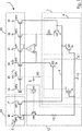
最初に、図1を参照すると、TlnT温度曲率補正(TlnT tenperature curvature correction)を有する温度的に安定なDC基準電圧出力を供給するための本発明によるバンドギャップ基準電圧回路(bandgap voltage reference circuit)が図示され、参照番号1によって概略的に示されている。基準電圧回路1は、CMOSプロセスによってシリコンチップ上に集積回路として実施されている。基準電圧回路1は、電源レール(supply rail)2に電源電圧(supply voltage)Vddが供給されており、基準電圧回路1はグランド3で接地されている。温度的に安定なTlnT温度曲率補正された基準電圧(the temperature stable TlnT temperature curvature corrected voltage reference)は、出力端子5とグランド3との間に発生される。
First, referring to FIG. 1, a bandgap voltage reference circuit according to the present invention for providing a temperature stable DC reference voltage output having TlnT temperature curvature correction is shown. Shown and schematically indicated by
基準電圧回路1はバンドギャップセル(bandgap cell)7を備え、このバンドギャップセル7は、二つのスタックドトランジスタ、即ち二つの第1トランジスタQ1,Q2から成る第1トランジスタスタック(first transistor stack)8と、二つのスタックドトランジスタ(stacked transistor)、即ち二つの第2トランジスタQ3,Q4から成る第2トランジスタスタック(second transistor stack)9とを備える。第1トランジスタスタック8および第2トランジスタスタック9は、第1トランジスタスタック8及び第2トランジスタスタック9のベース・エミッタ電圧ΔVbeにおける差分に比例した補正PTAT電圧を発生させるように構成される。換言すれば、補正PTAT電圧ΔVbeは、第2トランジスタQ3,Q4のベース・エミッタ電圧の和(sum)、および第1トランジスタQ1,Q2のベース・エミッタ電圧の和における電圧差に比例する。補正PTAT電圧ΔVbeは、主抵抗(primary resistor)R1を通して発生され、副抵抗(secondary resistor)R3上にスケーリングされる。副抵抗R3を通して発生された上記スケーリングされた補正PTAT電圧は、出力端子5とグランド3との間に基準電圧を提供するために、第1トランジスタスタック8の第1トランジスタQ1のベース・エミッタCTAT電圧と合算される。
The
第1トランジスタQ1,Q2及び第2トランジスタQ3,Q4のコレクタは、グランドに接続される。第1トランジスタスタック8および第2トランジスタスタック9における最低位(lowermost)の第1および第2トランジスタ、即ちトランジスタQ1およびQ3のベースもまたグランドに接続される。第1トランジスタスタック8および第2トランジスタスタック9における最高位(topmost)の第1トランジスタQ2および第2トランジスタQ4のベースは、各トランジスタスタック8および9の対応する第1トランジスタQ1および第2トランジスタQ3のエミッタに接続される。主抵抗R1は、第2トランジスタスタック9における最高位の第2トランジスタQ4のエミッタと、ハイインピーダンスの演算増幅器A1の反転入力との間に接続される。第1トランジスタスタック8における最高位の第1トランジスタQ2のエミッタは、演算増幅器A1の非反転入力に接続される。演算増幅器A1は、その反転入力および非反転入力上の電圧を共通の第1電圧レベルに駆動するために、第1カレントミラー回路10のMOSFET MP1から、その出力を通じて値Ifの電流I1を引き込む。演算増幅器A1によって引き込まれた電流は実質的にPTAT電流であり、従って第1カレントミラー回路10によって供給される電流は、同様に実質的にPTAT電流である。
The collectors of the first transistors Q1, Q2 and the second transistors Q3, Q4 are connected to the ground. The lowermost first and second transistors in the first transistor stack 8 and the second transistor stack 9, ie, the bases of the transistors Q1 and Q3, are also connected to ground. The topmost bases of the first transistor Q2 and the second transistor Q4 in the first transistor stack 8 and the second transistor stack 9 are the bases of the corresponding first transistor Q1 and second transistor Q3 of each transistor stack 8 and 9, respectively. Connected to the emitter. The main resistor R1 is connected between the emitter of the second highest transistor Q4 in the second transistor stack 9 and the inverting input of the high impedance operational amplifier A1. The emitter of the highest first transistor Q2 in the first transistor stack 8 is connected to the non-inverting input of the operational amplifier A1. The operational amplifier A1 draws the current I1 of value If through its output from the MOSFET MP1 of the first
第2トランジスタスタック9の最高位の第2トランジスタQ4のエミッタには、主抵抗R1を介して第1カレントミラー回路10のMOSFET MP2から値IfのPTAT電流I2が供給される。第2トランジスタスタック9の最低位の第2トランジスタQ3のエミッタには、第1カレントミラー回路10のMOSFET MP3を介して値IfのPTAT電流I3が供給される。第1トランジスタスタック8の最高位の第1トランジスタQ2のエミッタには、第1カレントミラー回路10のMOSFET MP4により値n4IfのPTAT電流I4が供給される。第1トランジスタスタック8の最低位の第1トランジスタQ1のエミッタには、副抵抗R3上に主抵抗R1を通じて発生される補正PTAT電圧ΔVbeをスケーリングするために、第1カレントミラー回路10のMOSFET MP5により値(n3−1)・IfのPTAT電流I5が供給される。また、第1トランジスタスタック8の最低位の第1トランジスタQ1のエミッタには、以下に説明される目的のために、第1カレントミラー回路10のMOSFET MP6を介して値Ifの電流I6が供給される。従って、最低位の第1トランジスタQ1のエミッタに供給される電流の合計はn3・Ifである。
The PTAT current I2 having a value If is supplied from the MOSFET MP2 of the first
第1トランジスタQ1,Q2および第2トランジスタQ3,Q4に供給されるPTAT電流の値と、第1トランジスタQ1,Q2および第2トランジスタQ3,Q4のエミッタ面積は、主抵抗R1を通して補正PTAT電圧ΔVbeを発生させるために、第1トランジスタQ1,Q2が動作する電流密度よりも第2トランジスタQ3,Q4が動作する電流密度が小さくなるように選択される。第1トランジスタスタック8の第1トランジスタQ1,Q2のエミッタ面積は同等(similar)であり、それぞれ単位面積とする。第2トランジスタスタック9の最低位の第2トランジスタQ3のエミッタ面積は、第1トランジスタスタック8の最低位の第1トランジスタQ1のエミッタ面積よりも大きく、本発明のこの実施形態では、最低位の第1トランジスタQ1のエミッタ面積のn1倍の面積である。第2トランジスタスタック9の最高位の第2トランジスタQ4のエミッタ面積は、第1トランジスタスタック8の最高位の第1トランジスタQ2のエミッタ面積よりも大きく、本発明のこの実施形態では、最高位の第1トランジスタQ2のエミッタ面積のn2倍の面積であり、従って最低位の第1トランジスタQ1のエミッタ面積のn2倍の面積でもある。 The values of the PTAT current supplied to the first transistors Q1, Q2 and the second transistors Q3, Q4 and the emitter areas of the first transistors Q1, Q2 and the second transistors Q3, Q4 are corrected with the corrected PTAT voltage ΔV be through the main resistor R1. Is selected so that the current density at which the second transistors Q3 and Q4 operate is smaller than the current density at which the first transistors Q1 and Q2 operate. The emitter areas of the first transistors Q1 and Q2 of the first transistor stack 8 are similar, and each has a unit area. The emitter area of the lowest second transistor Q3 in the second transistor stack 9 is larger than the emitter area of the lowest first transistor Q1 in the first transistor stack 8, and in this embodiment of the present invention, the lowest second transistor Q3. 1 is n 1 times the area of the emitter area of the transistor Q1. The emitter area of the highest second transistor Q4 of the second transistor stack 9 is larger than the emitter area of the highest first transistor Q2 of the first transistor stack 8, and in this embodiment of the present invention, the highest second transistor Q4. 1 transistor Q2 is n 2 times the area of the emitter area, and therefore is also a n 2 times the area of the emitter area of the first transistor Q1 of the lowest.
CTAT電流発生回路12は、ライン14上に値IcrのCTAT補正電流I7を供給し、この電流は、以下に説明されるように、最低位の第1トランジスタQ1のベース・エミッタCTAT電圧のTlnT温度曲率成分と相補的(complementary)であるTlnT温度曲率成分を有する主抵抗R1を通じて発生された補正PTAT電圧ΔVbeを提供するために、PTAT電流I3と合算されて第2トランジスタスタック9の最低位の第2トランジスタQ3のエミッタに供給される。CTAT電流発生回路12は抵抗R2を備え、この抵抗を通じて、第1トランジスタスタック8の最低位の第1トランジスタQ1のベース・エミッタCTAT電圧がダイオード接続されたMOSFET MN1とMOSFET MN2とを介して反射される。抵抗R2を通じたベース・エミッタCTAT電圧は、第2カレントミラー回路15のMOSFET MP8を介して値IcrのCTAT電流I8を抵抗R2に引き込ませる。抵抗R2によって引き込まれた値Icrの電流I8は、MOSFET MP7によって第2カレントミラー回路15においてミラーリングされ、MOSFET MP7は、値IcrのCTAT補正電流をライン14上に供給する。
The CTAT
主抵抗R1を通じて発生される補正PTAT電圧ΔVbeのTlnT温度曲率成分を発生させるために最低位の第2トランジスタQ3に供給されるPTAT電流I3の値Ifに対するCTAT補正電流I7の値Icrの比は、補正PTAT電圧が主抵抗R1から副抵抗R3に反射される利得係数(gain factor)の関数であり、また、以下にσとして説明される飽和電流温度指数(saturation current temperature exponent)の関数でもある。拡散シリコン接合(diffused silicon junction)についての飽和電流温度指数の値は、一般には約4である。従って、例えば、もし副抵抗R3を通じて発生されるスケーリングされた補正PTAT電圧が、主抵抗R1を通じて発生される補正PTAT電圧から2の利得係数だけスケールアップ(scaled up)され、且つもし飽和電流温度指数が4であれば、最低位の第2トランジスタQ3のエミッタに供給される電流は温度的に独立であるはずである。換言すれば、PTAT電流の値IfとCTAT補正電流の値Icrとの和は、温度にかかわりなく一定であるはずである。これは、最低位の第2トランジスタQ3のエミッタに供給されるPTAT電流の値Ifに対するCTAT補正電流の値Icrの比を1にすることにより達成される。換言すれば、CTAT補正電流の値Icrは、最低位の第2トランジスタQ3のエミッタに供給されるPTAT電流の値Ifと等しく設定されるべきである。これは、MOSFET MP7,MP8が適切な面積になるように選択することにより達成される。他方、もし、飽和電流温度指数が4よりも大きければ、適切なTlnT温度曲率成分を有する主抵抗R1を通じて発生される補正PTAT電圧を提供するために、CTAT補正電流の値Icrは、最低位の第2トランジスタQ3のエミッタに供給されるPTAT電流I3の値Ifよりも大きくなるべきである。飽和電流温度指数の値が大きくなる程、主抵抗R1から副抵抗R3への補正PTAT電圧の所定の利得係数について必要とされるCTAT補正電流の値Icrが大きくなる。 Is generated primarily through resistor R1 correction PTAT voltage [Delta] V BE TlnT temperature curvature of PTAT current I3 supplied to the second transistor Q3 of the lowest to generate the component values of I cr of CTAT correcting current I7 for I f in The ratio is a function of the gain factor at which the corrected PTAT voltage is reflected from the main resistor R1 to the sub-resistor R3, and a function of the saturation current temperature exponent, which is described below as σ. But there is. The value of the saturation current temperature index for a diffused silicon junction is typically about 4. Thus, for example, if the scaled corrected PTAT voltage generated through the secondary resistor R3 is scaled up by a gain factor of 2 from the corrected PTAT voltage generated through the main resistor R1, and if the saturation current temperature index Is 4, the current supplied to the emitter of the lowest second transistor Q3 should be temperature independent. In other words, the sum of the PTAT current value If and the CTAT correction current value Icr should be constant regardless of the temperature. This is achieved by setting the ratio of the CTAT correction current value I cr to the PTAT current value If supplied to the emitter of the lowest second transistor Q3 to 1. In other words, the CTAT correction current value I cr should be set equal to the PTAT current value If supplied to the emitter of the lowest second transistor Q3. This is achieved by selecting the MOSFETs MP7 and MP8 to have an appropriate area. On the other hand, if the saturation current temperature index is greater than 4, in order to provide a corrected PTAT voltage generated through the main resistor R1 having an appropriate TlnT temperature curvature component, the CTAT correction current value I cr is at the lowest level. Should be larger than the value If of the PTAT current I3 supplied to the emitter of the second transistor Q3. As the value of the saturation current temperature index increases, the CTAT correction current value I cr required for a predetermined gain coefficient of the correction PTAT voltage from the main resistor R1 to the sub resistor R3 increases.
ここで、バンドギャップ基準電圧回路1の動作の背景にある理論を説明する。
絶対温度T°ケルビンでのバイポーラトランジスタのベース・エミッタ電圧の公知の数式は次のようである。
Here, the theory behind the operation of the band gap
A well-known formula for the base-emitter voltage of a bipolar transistor at an absolute temperature T ° Kelvin is:

ここで、Vbe(T)は、T°ケルビンでのバイポーラトランジスタについての温度依存のベース・エミッタ電圧である。
VG0は、シリコンについて約1.205Vを仮定した場合のバンドギャップエネルギー電圧である。
Tは、度ケルビンでの動作絶対温度である。
T0は、度ケルビンでの基準温度(通常、動作温度範囲の中間点)である。
Vbe0は、基準温度T0でのバイポーラトランジスタのベース・エミッタ電圧である。
kは、ボルツマン定数である。
qは、電子の電荷量である。
σは、飽和電流温度指数(SPICE TM 回路シミュレーションプログラムではXTIと称され、拡散シリコン接合については約4の値を有する)である。
Icは、バイポーラトランジスタのコレクタ電流である。
Ic0は、基準温度T0でのバイポーラトランジスタのコレクタ電流である。
Where V be (T) is the temperature dependent base-emitter voltage for a bipolar transistor at T ° Kelvin.
V G0 is a bandgap energy voltage assuming about 1.205 V for silicon.
T is the operating absolute temperature in degrees Kelvin.
T 0 is the reference temperature in degrees Kelvin (usually the midpoint of the operating temperature range).
V be0 is the base-emitter voltage of the bipolar transistor at the reference temperature T 0 .
k is a Boltzmann constant.
q is the charge amount of electrons.
σ is the saturation current temperature index (referred to as XTI in the SPICE ™ circuit simulation program and having a value of about 4 for diffusion silicon junctions).
I c is the collector current of the bipolar transistor.
I c0 is the collector current of the bipolar transistor at the reference temperature T 0 .
数式(1)における最初の2つの項は、温度の増加に伴うベース・エミッタ電圧の線形減少を示す。この数式における最後の2つの項は、ベース・エミッタ電圧の非線形項であり、電圧の未補正温度曲率成分として知られる。
第1トランジスタQ1,Q2および第2トランジスタQ4は、次のように、PTAT電流でバイアスされる。
The first two terms in equation (1) show a linear decrease in base-emitter voltage with increasing temperature. The last two terms in this equation are non-linear terms of the base-emitter voltage, known as the uncorrected temperature curvature component of the voltage.
The first transistors Q1, Q2 and the second transistor Q4 are biased with the PTAT current as follows.
従って、温度T°ケルビンでの第1トランジスタQ1,Q2および第2トランジスタQ4のベース・エミッタ電圧は、次の3つの数式で与えられる。
最低位の第1トランジスタQ1については次の式である。
Accordingly, the base-emitter voltages of the first transistors Q1, Q2 and the second transistor Q4 at the temperature T ° Kelvin are given by the following three equations.
The lowest level first transistor Q1 is represented by the following equation.
最高位の第1トランジスタQ2については次の式である。 The highest level first transistor Q2 is represented by the following equation.
最高位の第2トランジスタQ4については次の式である。 The highest level second transistor Q4 is given by the following equation.
最低位の第2トランジスタQ3は、異なる電流、即ち値IfのPTAT電流I3に値IcrのCTAT電流I7をプラスしたものでバイアスされる。従って、第3トランジスタQ3については次のようになる。 The second transistor Q3 of the lowest positions are different currents, that is, biasing the CTAT current I7 of the PTAT current I3 value I f value I cr in those positive. Therefore, the third transistor Q3 is as follows.
ここで、nは、最低位の第2トランジスタQ3のエミッタ電流の負温度指数(negative temperature exponent)である。従って、温度的に独立な一定電流についてはn=0であり、PTAT電流についてはn=−1である。 Here, n is a negative temperature exponent of the emitter current of the lowest second transistor Q3. Therefore, n = 0 for a temperature independent constant current and n = -1 for a PTAT current.
よって、数式(6)による電流で最低位の第2トランジスタQ3がバイアスされた状態では、温度T°ケルビンでの最低位の第2トランジスタQ3のベース・エミッタ電圧は、次のようになる。 Therefore, in a state where the lowest second transistor Q3 is biased with the current of Equation (6), the base-emitter voltage of the lowest second transistor Q3 at the temperature T ° Kelvin is as follows.
従って、基準温度T0での第1トランジスタQ1,Q2および第2トランジスタQ3,Q4のベース・エミッタ電圧は次のようになる。
最低位の第1トランジスタQ1については次の式である。
Accordingly, the first transistor Q1 at a reference temperature T 0, Q2 and the base-emitter voltage of the second transistors Q3, Q4 are as follows.
The lowest level first transistor Q1 is represented by the following equation.
最高位の第1トランジスタQ2については次の式である。 The highest level first transistor Q2 is represented by the following equation.
最高位の第2トランジスタQ4については次の式である。 The highest level second transistor Q4 is given by the following equation.
最低位の第2トランジスタQ3については次の式である。 The lowest level second transistor Q3 is represented by the following equation.
ここで、Isは、第1トランジスタQ1,Q2および第2トランジスタQ3,Q4の飽和電流であり、エミッタ面積に比例し、且つ、温度およびプロセスに強く依存する。Ifは、第1カレントミラー回路において発生されるPTAT電流であり、n3およびn4は、図1におけるPTAT電流Ifについてのスケーリング値であり、n1およびn2は、図1を参照して上述した第1トランジスタQ1,Q2のエミッタ面積にそれぞれ対する第2トランジスタQ3,Q4のエミッタ面積の比率である。 Here, I s is a first transistor Q1, Q2 and the saturation current of the second transistor Q3, Q4, proportional to the emitter area, and is strongly dependent on temperature and process. I f is the PTAT current generated in the first current mirror circuit, n 3 and n 4, a scaling value for the PTAT current I f in Fig. 1, n 1 and n 2, see Figure 1 The ratio of the emitter areas of the second transistors Q3 and Q4 to the emitter areas of the first transistors Q1 and Q2 described above.
数式(8),(9),(10),(11)において、エミッタおよびコレクタ電流は同一であり、且つ飽和電流Isはエミッタ面積に比例すると仮定できる。
従って、主抵抗R1を通じて発生される電圧ΔVbeは次の数式で与えられる。
Equation (8), (9), (10), (11), emitter and collector currents are the same, and the saturation current I s can be assumed to be proportional to the emitter area.
Therefore, the voltage ΔV be generated through the main resistor R1 is given by the following equation.
数式(3)ないし(7)および(8)ないし(11)から、数式(12)は次のようになる。 From Expressions (3) to (7) and (8) to (11), Expression (12) is as follows.
数式(13)は次のように書き直すことができる。 Equation (13) can be rewritten as follows.
第1トランジスタQ1,Q2が、それぞれ単位エミッタ面積を有すると仮定すると、次のようになる。
IsQ1=IsQ2=Is
最低位の第2トランジスタQ3は、最低位の第1トランジスタQ1のエミッタ面積よりもn1倍大きなエミッタ面積を有するので、最低位の第2トランジスタQ3についての飽和電流は次のようになる。
IsQ3=n1Is
最高位の第2トランジスタQ4についての飽和電流は次のようになる。
IsQ4=n2Is
Assuming that the first transistors Q1 and Q2 each have a unit emitter area, the following is obtained.
I sQ1 = I sQ2 = I s
Since the lowest-order second transistor Q3 has an emitter area n 1 times larger than that of the lowest-order first transistor Q1, the saturation current for the lowest-order second transistor Q3 is as follows.
I sQ3 = n 1 I s
The saturation current for the second highest transistor Q4 is as follows.
I sQ4 = n 2 I s
最低位の第1トランジスタQ1についてのコレクタ電流は次のようになる。
Ic1=(n3−1)If+If=n3If
最高位の第1トランジスタQ2についてのコレクタ電流は次のようになる。
Ic2=n4If
最低位の第2トランジスタQ3は、If(PTAT)のコレクタ電流にCTAT補正電流Icrをプラスしたものを有し、CTAT補正電流Icr=Vbe1/R2であり、ここで、R2は抵抗R2の抵抗値である。
最高位の第2トランジスタQ4のコレクタ電流はIc4=Ifである。
The collector current for the lowest first transistor Q1 is as follows.
I c1 = (n 3 −1) I f + I f = n 3 If
The collector current for the highest first transistor Q2 is as follows.
I c2 = n 4 If
The second transistor Q3 of the lowest has those plus CTAT correcting current I cr the collector current of I f (PTAT), a CTAT correcting current I cr = V be1 / R 2 , where, R 2 Is the resistance value of the resistor R2.
The collector current of the second highest transistor Q4 is I c4 = If .
出力端子5とグランド3との間にバンドギャップ基準電圧回路1により発生される基準電圧Vrefは、最低位の第1トランジスタQ1のベース・エミッタ電圧に抵抗R3を通じた電圧降下をプラスしたものに等しく、それは次の数式で与えられる。
The reference voltage V ref generated by the band gap
ここで、R1およびR3は、それぞれ、主抵抗R1および副抵抗R3の抵抗値である。
数式(15)は次のように書き直すことができる。
Here, R 1 and R 3 are resistance values of the main resistor R1 and the sub resistor R3, respectively.
Equation (15) can be rewritten as follows.
ここで、 here,
且つ and
基準電圧Vrefが温度に対して独立であるために、AおよびBの値はゼロでなければならない。 In order for the reference voltage V ref to be independent of temperature, the values of A and B must be zero.
AおよびBの値をゼロに設定するための多くのオプションが存在する。一つのオプションは、温度的に独立な一定電流を最低位の第2トランジスタQ3に強制的に供給することである。室温で互いに等しくなるように第2トランジスタQ3のエミッタにそれぞれ供給されるCTAT補正電流の値IcrおよびPTAT電流の値Ifを選択することにより、第2トランジスタQ3のエミッタ電流は一定であり且つ温度的に独立である。第2トランジスタQ3のエミッタ電流がそのように選択されると、基準温度(reference temperature)での第2トランジスタQ3のエミッタ電流の数式は次のようになる。 There are many options for setting the values of A and B to zero. One option is to force a constant temperature independent current to the lowest second transistor Q3. By selecting the CTAT correction current value I cr and the PTAT current value If that are respectively supplied to the emitter of the second transistor Q3 so as to be equal to each other at room temperature, the emitter current of the second transistor Q3 is constant and Temperature independent. When the emitter current of the second transistor Q3 is so selected, the formula for the emitter current of the second transistor Q3 at the reference temperature is:
Bの値は、次のようにゼロに設定することができる。
最低位の第2トランジスタQ3のエミッタ電流は一定であるから、数式(6)の第2トランジスタQ3のエミッタ電流の負温度指数nはゼロに等しい。
従って、Bをゼロに等しくし、且つnをゼロに等しくすると、数式(18)は次のようになる。
The value of B can be set to zero as follows:
Since the emitter current of the lowest second transistor Q3 is constant, the negative temperature index n of the emitter current of the second transistor Q3 in equation (6) is equal to zero.
Thus, if B is equal to zero and n is equal to zero, equation (18) becomes:
数式(20)の左辺の項はPTAT利得を表す。この数式は、補正PTAT電圧の利得が最低位の第1トランジスタQ1のベース・エミッタ電圧の曲率電圧(K.T/q*log(T/T0))係数に等しくならなければならないことを示している。 The term on the left side of Equation (20) represents the PTAT gain. This formula shows that the gain of the corrected PTAT voltage must be equal to the curvature voltage (KT / q * log (T / T0)) coefficient of the base-emitter voltage of the lowest first transistor Q1. Yes.
拡散シリコン接合σが4に等しければ、3の利得が必要とされる。これは、抵抗比R3/R1および電流比n3を適切にスケーリングすることにより準備される。もし主抵抗R1および副抵抗R3が等しい抵抗値に選択されると、電流比n3が4に等しくなり得る。あるいは、副抵抗R3は、主抵抗R1の抵抗値の2倍に等しい抵抗値になるように選択されることができ、そして電流比n3は5/2に等しく設定されることができる。 If the diffusion silicon junction σ is equal to 4, then a gain of 3 is required. This is prepared by appropriately scaling the resistance ratio R 3 / R 1 and the current ratio n 3 . When if is selected on the main resistor R1 and the sub-resistor R3 equal resistance value, the current ratio n 3 may be equal to 4. Alternatively, the sub-resistor R3 may be selected to be the resistance value equal to twice the resistance value of the main resistor R1, and the current ratio n 3 can be set equal to 5/2.
数式(17)のAの値がゼロに等しくなるという条件を満たすために、主抵抗R1を通じて発生されるΔVbeの値を与えるためには、次のことが要求される。
もし、
In order to satisfy the condition that the value of A in Equation (17) is equal to zero, the following is required to provide the value of ΔV be generated through the main resistor R1.
if,
であれば、数式(17)よりn1・n2=81であり、従ってn1=n2=9である。 Then, n 1 · n 2 = 81 from equation (17), and therefore n 1 = n 2 = 9.
従って、室温で互いに等しくなるように第2トランジスタQ3にそれぞれ供給されるCTAT補正電流の値IcrおよびPTAT電流の値Ifを選択することにより、且つ、主抵抗R1および副抵抗R3が互いに等しい抵抗値になるように選択することにより、電流比n3が4に等しく、電流比n4が電流比n3に等しく、面積の比n1およびn2が互いに等しく且つ9に等しく、基準電圧Vrefが最低位の第1トランジスタQ1のバンドギャップ電圧VG0に等しくなり、従って温度的に独立になる。あるいは、もし副抵抗R3が主抵抗R1の抵抗値の2倍に等しい抵抗値となるように選択されれば、もし電流比n3が5/2に等しく設定され、且つ残りの変数が上述のように設定されれば、バンドギャップ基準電圧回路1の基準電圧Vrefは、最低位の第1トランジスタQ1のバンドギャップ電圧VG0に等しくなる。
Accordingly, by selecting the CTAT correction current value I cr and the PTAT current value If that are respectively supplied to the second transistor Q3 so as to be equal to each other at room temperature, the main resistance R1 and the sub resistance R3 are equal to each other. By choosing a resistance value, the current ratio n 3 is equal to 4, the current ratio n 4 is equal to the current ratio n 3 , the area ratios n 1 and n 2 are equal to each other and equal to 9, and the reference voltage V ref is equal to the bandgap voltage V G0 of the lowest first transistor Q1, and is therefore temperature independent. Alternatively, if it vice resistor R3 is selected such that the resistance value is equal to twice the resistance value of the main resistor R1, if the current ratio n 3 are set equal to 5/2, and the remaining variables are described above With this setting, the reference voltage V ref of the band gap
AおよびBの値をゼロに設定するための別のオプションは、エミッタに強制的に供給される電流が主にCTAT電流であるように最低位の第2トランジスタQ3のエミッタに供給されるPTAT電流に対するCTAT補正電流の比を選択することである。エミッタ電流の傾き(slope)が負になるように主なCTAT電流をトランジスタのエミッタに強制的に供給することによりベース・エミッタ温度曲率電圧が強調されることが知られている。従って、もしCTAT補正電流が最低位の第2トランジスタQ3のエミッタにおいて十分に支配的であれば、ベース・エミッタ温度曲率電圧は、補正PTAT電圧についての利得と曲率電圧係数とが2に等しいレベルで強調される。従って、数式(18)からのBの値がゼロに等しいことを保証するために、Bをゼロに等しいとした数式(18)は次のように書き直すことができる。 Another option for setting the values of A and B to zero is the PTAT current supplied to the emitter of the lowest second transistor Q3 so that the current forced to the emitter is mainly the CTAT current. The ratio of the CTAT correction current to is selected. It is known that the base-emitter temperature curvature voltage is enhanced by forcibly supplying the main CTAT current to the emitter of the transistor such that the slope of the emitter current is negative. Therefore, if the CTAT correction current is sufficiently dominant at the emitter of the lowest second transistor Q3, the base-emitter temperature curvature voltage is at a level where the gain and curvature voltage coefficient for the correction PTAT voltage are equal to 2. To be emphasized. Thus, to ensure that the value of B from equation (18) is equal to zero, equation (18) with B equal to zero can be rewritten as:
もし、n3=n4=3であり、且つ他の値が数式(21)に従えば、数式(6)の最低位の第2トランジスタQ3のエミッタ電流の負温度指数nは0.5に等しい。したがって、最低位の第2トランジスタQ3のエミッタに強制的に供給されるべき電流は、一定電流とCTAT電流との間の中間であるべきであり、従って次の数式が保持される。 If n 3 = n 4 = 3 and other values follow Formula (21), the negative temperature index n of the emitter current of the second lowest transistor Q3 in Formula (6) becomes 0.5. equal. Therefore, the current to be forcibly supplied to the emitter of the lowest second transistor Q3 should be between the constant current and the CTAT current, and therefore the following equation is maintained.
この例では、n1・n2=5502であり、従って、n1=n2=74である。
上述のことから、補正PTAT電圧の必要な利得が主として主抵抗R1の抵抗値に対する副抵抗R3の抵抗値の比および電流比n3から得られる事により、第2トランジスタQ3,Q4に必要とされるトランジスタ面積が比較的小さいので、一定の温度的に独立な電流を最低位の第2トランジスタQ3のエミッタに強制的に供給するオプションが、集積回路チップのシリコン面積が重要な要素である場合に好ましいオプションであることが明らかになるであろう。主にCTAT補正電流を最低位の第2トランジスタQ3のエミッタに強制的に供給するオプションは、第2トランジスタQ3,Q4に利用可能なシリコン面積が重要でない場合に好ましいオプションであろう。CTAT補正電流を最低位の第2トランジスタQ3に強制的に供給する後者のオプションは、第1および第2カレントミラー回路および演算増幅器A1のオフセットの影響を受けにくい。
In this example, n 1 · n 2 = 5502 and therefore n 1 = n 2 = 74.
From the foregoing, by obtained from the ratio and the current ratio n 3 of the resistance value of the secondary resistor R3 to the resistance value of the required gain of the correction PTAT voltage mainly primary resistance R1, it is required for the second transistors Q3, Q4 If the area of the integrated circuit chip is an important factor, the option to force a constant temperature independent current to the emitter of the lowest second transistor Q3 is a relatively small transistor area. It will become clear that this is a preferred option. The option of mainly forcing CTAT correction current to the emitter of the lowest second transistor Q3 would be the preferred option when the silicon area available for the second transistors Q3, Q4 is not important. The latter option for forcibly supplying the CTAT correction current to the lowest second transistor Q3 is less susceptible to the offsets of the first and second current mirror circuits and the operational amplifier A1.
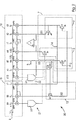
図2を参照すると、温度的に安定なTlnT曲率補正されたDC基準電圧を発生させるための、概略的に参照番号20によって示されたバンドギャップ基準電圧回路が図示されている。このバンドギャップ基準電圧回路20は、実質的に前記バンドギャップ基準電圧回路1と同様であり、同様の構成要素は同一の参照番号によって示されている。基準電圧回路20と基準電圧回路1との間の主な相違点は、第1較正回路21および第2較正回路22が、基準電圧回路20を較正するために備えられていることである。第1較正回路21は、CTAT補正電流I7の値Icrを微調整するために、最低位の第2トランジスタQ3のエミッタにライン14を介して供給される上記CTAT補正電流I7を較正するために備えられる。第1較正回路21は、CTAT較正電流ΔIcrを出力する第1プログラマブル電流デジタル/アナログ変換器(DAC)23を備え、CTAT較正電流ΔIcrは、ライン14を介して最低位の第2トランジスタQ3のエミッタに供給されるCTAT補正電流I7と合算される。CTAT較正電流ΔIcrは、MOSFET MP9を介して第2カレントミラー回路15から得られるCTAT電流I9から導き出される。CTAT較正電流ΔIcrの値は、第1電流DAC 23を適切にプログラムすることにより選択可能になっている。
Referring to FIG. 2, there is illustrated a bandgap reference voltage circuit, generally indicated by
第2較正回路22は、第2プログラマブル電流DAC 24を備え、この第2プログラマブル電流DAC 24には、MOSFET MP10を介して第1カレントミラー回路10から得られるPTAT電流I10が供給される。第2DAC 24は、副抵抗R3を通じて発生されるスケーリングされた補正PTAT電圧の比較的粗い調整と、最低位の第1トランジスタQ1のベース・エミッタCTAT電圧の微調整とを提供する。第2DAC 24は、副抵抗R3を通じて発生される補正PTAT電圧を調整するために、副抵抗R3を介して較正電流ΔIpcを供給し引き込む(source and sink)。較正電流ΔIpcの値とその方向は、第2DAC 24を適切にプログラムすることにより選択可能であり、これにより、副抵抗R3を通じて発生される補正PTAT電圧の上方調整および下方調整を可能にする。第2DAC 24が較正電流ΔIpcを供給し引き込むので、較正電流ΔIpcは、最低位の第1トランジスタQ1のエミッタ電流に何ら影響を及ぼさない。また、第2DAC 24は、最低位の第1トランジスタQ1のベース・エミッタCTAT電圧を微調整するために、最低位の第1トランジスタQ1に供給するための較正電流ΔIpfを供給することがプログラム可能となっている。
最終テスト(final test)と実装(packaging)中に第1DAC 23および第2DAC 24をプログラムするための不揮発性メモリ(図示なし)が備えられる。
The
Non-volatile memory (not shown) is provided for programming the
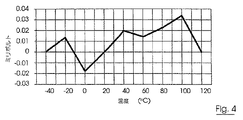
図3および図4を参照すると、図3は、図2のバンドギャップ基準電圧回路20のコンピュータシミュレーション上で実行されたシミュレーションテスト結果を示し、図4は、図2のバンドギャップ基準電圧回路20のCMOS実施上で実行されたテスト結果を示す。図3は、−42℃ないし+85℃の温度範囲にわたる温度に対してプロットされたバンドギャップ基準電圧回路のミリボルトでの3つの電圧波形を示す。波形Aは、図に示すように、出力端子5とグランド6との間に発生される基準電圧Vrefを示し、−42℃ないし+85℃の全温度範囲にわたって実質的に一定である。波形Bは、最低位の第1トランジスタQ1の未補正ベース・エミッタCTAT電圧を示し、一方、波形Cは副抵抗R3を通じて発生されるスケーリングされた補正PTAT電圧を示す。副抵抗R3を通じて発生された補正PTAT電圧は、最低位の第1トランジスタQ1の未補正ベース・エミッタCTAT電圧のTlnT温度曲率と相補的であるTlnT温度曲率を有している。
Referring to FIGS. 3 and 4, FIG. 3 shows a simulation test result executed on a computer simulation of the band gap
図4は、−40℃ないし+120℃の温度範囲にわたる拡大スケールでの直線一定電圧(straight line constant voltage)からのバンドギャップ基準電圧回路20の基準電圧Vrefの偏差(deviation)のプロットを示す。電圧は、度摂氏での温度に対するミリボルトでプロットされている。図に示すように、直線一定電圧からの最大の正の偏差(maximum positive deviation)は100℃で起こり、0.034ミリボルトよりも大きくなく、一方、最大の負の偏差は0℃で起こり、ほんの0.018ミリボルトである。
FIG. 4 shows a plot of the deviation of the reference voltage V ref of the bandgap
従って、出力端子5とグランド3との間に出力される基準電圧Vrefは実質的に一定を維持し、且つ、−40℃ないし+120℃の広い温度範囲にわたって実質的に温度的に独立(temperature independent)である。
Therefore, the reference voltage V ref output between the output terminal 5 and the
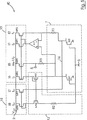
図5を参照すると、本発明の他の実施形態によるバンドギャップ基準電圧回路を示し、参照番号40で概略的に示されている。バンドギャップ基準電圧回路40は、実質的に図1のバンドギャップ基準電圧回路と同様であり、同様の構成要素は同一の参照番号によって示されている。バンドギャップ基準電圧回路40と回路1との間の主な相違点は、主抵抗R1を通じて差電圧ΔVbeを発生させるための第1および第2トランジスタの第1および第2スタックから成るバンドギャップセル7に代えて、バンドギャップセル7が、ただ一つの第1バイポーラトランジスタQ1と、ただ一つの第2バイポーラトランジスタQ3とを備えることである。第2トランジスタQ3のエミッタ面積は、図1のバンドギャップ基準電圧回路を参照して説明したように、第1トランジスタQ1のエミッタ面積のn1倍である。第2トランジスタQ3のエミッタには、主抵抗R1を介して値IfのPTAT電流I2が供給される。CTAT補正電流Icrは、ライン14を介して第2トランジスタQ3のエミッタに供給される。第1トランジスタQ1には、副抵抗R3を介して値(n3−1)・IfのPTAT電流I5が供給される。基準電圧は、端子5とグランド3との間に発生される。トランジスタQ2,Q4がバンドギャップ基準電圧回路40から省かれたので、PTAT電流I3,I4は必要とされず、従ってMOSFET MP3,MP4が第1カレントミラー10から省かれている。
Referring to FIG. 5, a bandgap reference voltage circuit according to another embodiment of the present invention is shown and schematically indicated by
それ以外は、図5のバンドギャップ基準電圧回路40は図1のものと同様であり、主抵抗R1を通じて発生されるPTAT差電圧ΔVbeは、第1および第2トランジスタQ1,Q3のベース・エミッタ電圧における差分に比例し、且つ副抵抗R3上にスケーリングされる。
Otherwise, the bandgap
図1を参照して述べられたバンドギャップ基準電圧回路が、二つのトランジスタからそれぞれ構成される第1および第2トランジスタスタックを備えるものとして説明されたが、第1および第2トランジスタスタックが2以上のトランジスタを備えてもよいことが構想される。ただし、各トランジスタスタックにおけるトランジスタの数は同じ(similar)である。 Although the bandgap reference voltage circuit described with reference to FIG. 1 has been described as including first and second transistor stacks each composed of two transistors, there are two or more first and second transistor stacks. It is envisioned that other transistors may be provided. However, the number of transistors in each transistor stack is the same.
また、必要なエミッタ面積を獲得するために、第1および第2トランジスタスタックにおける各トランジスタは複数のトランジスタによって提供されてもよいことが理解されるであろう。例えば、第1トランジスタは、それぞれ、単位エミッタ面積の各単一トランジスタとして提供されてもよく、一方、第2トランジスタスタックにおける対応トランジスタは、それぞれ、多数のトランジスタとして提供されてもよく、単位エミッタ面積のそれぞれは合算して適切なエミッタ面積になる。 It will also be appreciated that each transistor in the first and second transistor stacks may be provided by a plurality of transistors to obtain the required emitter area. For example, each first transistor may be provided as each single transistor of unit emitter area, while each corresponding transistor in the second transistor stack may be provided as multiple transistors, each having a unit emitter area. Each of these will add up to an appropriate emitter area.
PTATおよびCTAT電流は、カレントミラー回路から得られるものとして説明されたが、このようなPTATおよびCTAT電流を発生させるための他の如何なる適切な手段も、本発明の範囲を逸脱することなく使用できる。
また、演算増幅器の他に第1電圧レベルを発生させるための他の手段が使用できることも理解される。
Although PTAT and CTAT currents have been described as being derived from current mirror circuits, any other suitable means for generating such PTAT and CTAT currents can be used without departing from the scope of the present invention. .
It will also be appreciated that other means for generating the first voltage level besides the operational amplifier can be used.
或る場合には、主抵抗は、第2トランジスタスタックの最高位の第2トランジスタのエミッタと演算増幅器の反転入力との間に接続される以外に、第2トランジスタスタックにおける位置に備えられてもよいことが構想される。例えば、或る場合には、主抵抗は、任意の二つのスタックされた第2トランジスタ間に配置されてもよいことが構想される。 In some cases, the main resistor may be provided at a position in the second transistor stack in addition to being connected between the emitter of the second highest transistor in the second transistor stack and the inverting input of the operational amplifier. Good things are envisioned. For example, it is envisioned that in some cases the main resistor may be placed between any two stacked second transistors.
CTAT補正電流が、第2トランジスタスタックの最低位の第2トランジスタのエミッタに供給されるものとして説明されたが、必ずしもCTAT補正電流が最低位の第2トランジスタに供給される必要はなく、このCTAT補正電流が、第2トランジスタスタックの第2トランジスタのうちの任意の一つのエミッタに供給されてもよいことが理解されるであろう。実際に、或る場合には、CTAT補正電流が第2トランジスタスタックの第2トランジスタのうちの一つよりも多くのエミッタに供給されてもよいことが構想される。 Although the CTAT correction current has been described as being supplied to the emitter of the lowest second transistor of the second transistor stack, the CTAT correction current need not necessarily be supplied to the lowest second transistor. It will be appreciated that the correction current may be supplied to any one of the second transistors of the second transistor stack. Indeed, it is envisioned that in some cases the CTAT correction current may be supplied to more emitters than one of the second transistors of the second transistor stack.
主抵抗R1を通じて発生される相補的なTlnT温度曲率補正を有する補正PTAT電圧が、副抵抗R3上に反射されるものとして説明されたが、或る場合において、主抵抗から副抵抗に補正PTAT電圧をスケーリングすることが必ずしも必要でないことは当業者には即座に明白であろう。副抵抗を通じて発生される補正PTAT電圧の値は、主抵抗を通じて発生される値と同じであってもよい。また、相補的なTlnT温度曲率補正を有する補正PTAT電圧は、第1トランジスタスタックにおけるトランジスタのうちの一つのほかに、任意のトランジスタの未補正トランジスタベース・エミッタCTAT電圧と結合されてもよいことが理解される。例えば、相補的なTlnT温度曲率補正を有する補正PTAT電圧は、バンドギャップセルの外部のトランジスタの未補正ベース・エミッタCTAT電圧と結合されてもよい。いずれの場合においても、副抵抗は、このようなトランジスタの未補正ベース・エミッタCTAT電圧と、TlnT温度曲率補正を有する補正PTAT電圧との合算を容易化するように構成されることが構想される。 Although the corrected PTAT voltage with complementary TlnT temperature curvature correction generated through the main resistor R1 has been described as being reflected on the sub-resistor R3, in some cases the corrected PTAT voltage from the main resistor to the sub-resistor It will be readily apparent to those skilled in the art that it is not necessary to scale the. The value of the corrected PTAT voltage generated through the sub resistance may be the same as the value generated through the main resistance. Also, the corrected PTAT voltage with complementary TlnT temperature curvature correction may be combined with the uncorrected transistor base-emitter CTAT voltage of any transistor in addition to one of the transistors in the first transistor stack. Understood. For example, a corrected PTAT voltage with complementary TlnT temperature curvature correction may be combined with the uncorrected base-emitter CTAT voltage of a transistor external to the bandgap cell. In either case, it is envisioned that the sub-resistor is configured to facilitate the sum of the uncorrected base-emitter CTAT voltage of such a transistor and the corrected PTAT voltage with TlnT temperature curvature correction. .
第1および第2トランジスタスタックの第1および第2トランジスタは、それらのコレクタが共通電圧レベルに保持されるものとして説明されたが、或る場合において、これは必ずしも必要ではないことが構想される。しかしながら、第1および第2トランジスタスタックの第1および第2トランジスタのコレクタを共通電圧レベルに保持することにより、本発明によるバンドギャップ基準電圧回路は、とりわけCMOSプロセスでの製造に適する。 Although the first and second transistors of the first and second transistor stacks have been described as having their collectors held at a common voltage level, it is envisioned that in some cases this is not necessary. . However, by keeping the collectors of the first and second transistors of the first and second transistor stacks at a common voltage level, the bandgap voltage reference circuit according to the present invention is particularly suitable for manufacturing in a CMOS process.
1,20,40 バンドギャップ基準電圧回路
7 バンドギャップセル
8 第1トランジスタスタック
9 第2トランジスタスタック
10 第1カレントミラー回路
12 CTAT電流発生回路
15 第2カレントミラー回路
21 第1較正回路
22 第2較正回路
23 第1プログラマブル電流デジタル/アナログ変換器
24 第2プログラマブル電流デジタル/アナログ変換器
A1 演算増幅器
1, 20, 40 Band gap reference voltage circuit 7 Band gap cell 8 First transistor stack 9
Claims (35)
少なくとも一つの第1トランジスタと少なくとも一つの第2トランジスタとにPTAT電流をそれぞれ供給するステップであって、前記少なくとも一つのの第2トランジスタには主抵抗を通じて対応のPTAT電流が供給されるステップと、
前記第1及び第2トランジスタのベース・エミッタ電圧における差分に対応した補正PTAT電圧を主抵抗の端子間に発生させるために前記少なくとも一つの第1トランジスタ及び前記少なくとも一つの第2トランジスタが前記主抵抗と協調動作するように、前記少なくとも一つの第1トランジスタが動作される電流密度よりも低い電流密度で前記少なくとも一つの第2トランジスタを動作させるステップと、
前記基準電圧を発生させるために前記補正PTAT電圧を未補正トランジスタベース・エミッタCTAT電圧と結合するステップとを含み、
更に、
CTAT補正電流を、前記未補正トランジスタベース・エミッタCTAT電圧の前記TlnT温度曲率と相補的な曲率を有する前記補正PTAT電圧を前記主抵抗の端子間に発生させるために前記PTAT電流と共に前記少なくとも一つの第2トランジスタのうちの一つの第2トランジスタに供給し、これにより、前記未補正トランジスタベース・エミッタCTAT電圧と前記主抵抗の端子間に発生される前記補正PTAT電圧との結合電圧は、温度的に安定であり且つTlnT温度曲率が補正された基準電圧を供給するステップを含む方法。A method for generating a temperature stable bandgap reference voltage having a TlnT temperature curvature correction,
A respectively supplying step a PTAT current and one second transistor even without least at least one first transistor, the corresponding steps of the PTAT current is supplied through the main resistance to the at least one of the second transistor When,
The at least one first transistor and the at least one second transistor are configured to generate a corrected PTAT voltage corresponding to a difference in base-emitter voltage between the first and second transistors between terminals of the main resistor. Operating the at least one second transistor at a current density lower than a current density at which the at least one first transistor is operated to cooperate with
Combining the corrected PTAT voltage with an uncorrected transistor base-emitter CTAT voltage to generate the reference voltage;
Furthermore,
The at least one of the PTAT currents together with the PTAT current to generate a corrected PTAT voltage between terminals of the main resistor having a curvature complementary to the TlnT temperature curvature of the uncorrected transistor base-emitter CTAT voltage. The second transistor of one of the second transistors is supplied, whereby a combined voltage of the uncorrected transistor base-emitter CTAT voltage and the corrected PTAT voltage generated between the terminals of the main resistor is a temperature. how to stable and TlnT temperature curvature comprises the step that to supply corrected reference voltage.
少なくとも一つの第1トランジスタと少なくとも一つの第2トランジスタとにPTAT電流をそれぞれ供給するステップであって、前記少なくとも一つのの第2トランジスタには主抵抗を通じて対応のPTAT電流が供給されるステップと、
前記少なくとも一つの第1トランジスタ及び前記少なくとも一つの第2トランジスタが、前記第1及び第2トランジスタのベース・エミッタ電圧における差分に対応した補正PTAT電圧を主抵抗の端子間に発生させるために前記主抵抗と協調動作するように、前記少なくとも一つの第1トランジスタが動作される電流密度よりも低い電流密度で前記少なくとも一つの第2トランジスタを動作させるステップとを含み、
更に、
前記未補正トランジスタベース・エミッタCTAT電圧の前記TlnT温度曲率と相補的な曲率を有する前記PTAT電圧を前記主抵抗の端子間に発生させるために前記PTAT電流と共にCTAT補正電流を前記少なくとも一つの第2トランジスタのうちの一つの第2トランジスタに供給するステップを含む方法。A method for generating a PTAT voltage having a curvature complementary to an uncorrected TlnT temperature curvature of a base-emitter CTAT voltage of a transistor , comprising:
A respective supplying steps PTAT current and one second transistor even without least at least one first transistor, the corresponding steps of the PTAT current is supplied through the main resistance to the at least one of the second transistor When,
The at least one first transistor and the at least one second transistor cause the main PT to generate a corrected PTAT voltage corresponding to a difference in the base-emitter voltage of the first and second transistors. Operating the at least one second transistor at a current density lower than a current density at which the at least one first transistor is operated so as to cooperate with a resistor ;
Furthermore,
A CTAT correction current together with the PTAT current to generate the PTAT voltage having a curvature complementary to the TlnT temperature curvature of the uncorrected transistor base-emitter CTAT voltage between the terminals of the main resistor . Providing a second transistor of one of the transistors .
Applications Claiming Priority (2)
| Application Number | Priority Date | Filing Date | Title |
|---|---|---|---|
| US10/375,593 US6828847B1 (en) | 2003-02-27 | 2003-02-27 | Bandgap voltage reference circuit and method for producing a temperature curvature corrected voltage reference |
| PCT/IE2004/000025 WO2004077192A1 (en) | 2003-02-27 | 2004-02-23 | A bandgap voltage reference circuit and a method for producing a temperature curvature corrected voltage reference |
Publications (2)
| Publication Number | Publication Date |
|---|---|
| JP2006519433A JP2006519433A (en) | 2006-08-24 |
| JP4476276B2 true JP4476276B2 (en) | 2010-06-09 |
Family
ID=32926268
Family Applications (1)
| Application Number | Title | Priority Date | Filing Date |
|---|---|---|---|
| JP2006502617A Expired - Fee Related JP4476276B2 (en) | 2003-02-27 | 2004-02-23 | Band gap reference voltage circuit and method for generating temperature curvature corrected reference voltage |
Country Status (5)
| Country | Link |
|---|---|
| US (1) | US6828847B1 (en) |
| EP (1) | EP1599776B1 (en) |
| JP (1) | JP4476276B2 (en) |
| CN (1) | CN100527040C (en) |
| WO (1) | WO2004077192A1 (en) |
Families Citing this family (59)
| Publication number | Priority date | Publication date | Assignee | Title |
|---|---|---|---|---|
| US7071673B2 (en) * | 2003-09-02 | 2006-07-04 | Acu Technology Semiconductor Inc. | Process insensitive voltage reference |
| US7543253B2 (en) * | 2003-10-07 | 2009-06-02 | Analog Devices, Inc. | Method and apparatus for compensating for temperature drift in semiconductor processes and circuitry |
| US7211993B2 (en) * | 2004-01-13 | 2007-05-01 | Analog Devices, Inc. | Low offset bandgap voltage reference |
| US7019677B1 (en) * | 2004-09-08 | 2006-03-28 | Cirrus Logic, Inc. | Current steering digital to analog converters with self-calibration, and systems and methods using the same |
| US7486065B2 (en) * | 2005-02-07 | 2009-02-03 | Via Technologies, Inc. | Reference voltage generator and method for generating a bias-insensitive reference voltage |
| KR100605258B1 (en) | 2005-02-28 | 2006-07-31 | 삼성전자주식회사 | Reference voltage providing circuit with ultra low power consumption |
| US7204638B2 (en) * | 2005-05-23 | 2007-04-17 | Etron Technology, Inc. | Precise temperature sensor with smart programmable calibration |
| JP2006338434A (en) * | 2005-06-03 | 2006-12-14 | New Japan Radio Co Ltd | Reference voltage generation circuit |
| US20070052473A1 (en) * | 2005-09-02 | 2007-03-08 | Standard Microsystems Corporation | Perfectly curvature corrected bandgap reference |
| CN100456197C (en) * | 2005-12-23 | 2009-01-28 | 深圳市芯海科技有限公司 | Reference voltage source for low temperature coefficient with gap |
| US7683701B2 (en) | 2005-12-29 | 2010-03-23 | Cypress Semiconductor Corporation | Low power Bandgap reference circuit with increased accuracy and reduced area consumption |
| SG134189A1 (en) * | 2006-01-19 | 2007-08-29 | Micron Technology Inc | Regulated internal power supply and method |
| US7331708B2 (en) * | 2006-02-23 | 2008-02-19 | National Semiconductor Corporation | Frequency ratio digitizing temperature sensor with linearity correction |
| US7411380B2 (en) * | 2006-07-21 | 2008-08-12 | Faraday Technology Corp. | Non-linearity compensation circuit and bandgap reference circuit using the same |
| US7710190B2 (en) * | 2006-08-10 | 2010-05-04 | Texas Instruments Incorporated | Apparatus and method for compensating change in a temperature associated with a host device |
| US7408400B1 (en) | 2006-08-16 | 2008-08-05 | National Semiconductor Corporation | System and method for providing a low voltage bandgap reference circuit |
| KR100795013B1 (en) * | 2006-09-13 | 2008-01-16 | 주식회사 하이닉스반도체 | Band gap reference circuit and temperature data output apparatus using the same |
| US8102201B2 (en) | 2006-09-25 | 2012-01-24 | Analog Devices, Inc. | Reference circuit and method for providing a reference |
| US7576598B2 (en) | 2006-09-25 | 2009-08-18 | Analog Devices, Inc. | Bandgap voltage reference and method for providing same |
| KR100790476B1 (en) * | 2006-12-07 | 2008-01-03 | 한국전자통신연구원 | Band-gap reference voltage bias for low voltage operation |
| US7714563B2 (en) * | 2007-03-13 | 2010-05-11 | Analog Devices, Inc. | Low noise voltage reference circuit |
| CN101266506B (en) * | 2007-03-16 | 2010-12-01 | 深圳赛意法微电子有限公司 | CMOS process band-gap reference voltage source without operation amplifier |
| US20080265860A1 (en) * | 2007-04-30 | 2008-10-30 | Analog Devices, Inc. | Low voltage bandgap reference source |
| KR100912093B1 (en) * | 2007-05-18 | 2009-08-13 | 삼성전자주식회사 | PTAT current generation circuit having high temperature coefficient, display device and method thereof |
| US7605578B2 (en) | 2007-07-23 | 2009-10-20 | Analog Devices, Inc. | Low noise bandgap voltage reference |
| US20090039949A1 (en) * | 2007-08-09 | 2009-02-12 | Giovanni Pietrobon | Method and apparatus for producing a low-noise, temperature-compensated bandgap voltage reference |
| US7636010B2 (en) * | 2007-09-03 | 2009-12-22 | Elite Semiconductor Memory Technology Inc. | Process independent curvature compensation scheme for bandgap reference |
| US7598799B2 (en) * | 2007-12-21 | 2009-10-06 | Analog Devices, Inc. | Bandgap voltage reference circuit |
| US7612606B2 (en) * | 2007-12-21 | 2009-11-03 | Analog Devices, Inc. | Low voltage current and voltage generator |
| US7880533B2 (en) * | 2008-03-25 | 2011-02-01 | Analog Devices, Inc. | Bandgap voltage reference circuit |
| US7750728B2 (en) * | 2008-03-25 | 2010-07-06 | Analog Devices, Inc. | Reference voltage circuit |
| US7902912B2 (en) | 2008-03-25 | 2011-03-08 | Analog Devices, Inc. | Bias current generator |
| JP2011525080A (en) * | 2008-06-19 | 2011-09-08 | クゥアルコム・インコーポレイテッド | Apparatus and method for tuning a Gm-C filter |
| US8710912B2 (en) | 2008-11-24 | 2014-04-29 | Analog Device, Inc. | Second order correction circuit and method for bandgap voltage reference |
| US8390363B2 (en) * | 2008-11-25 | 2013-03-05 | Linear Technology Corporation | Circuit, trim and layout for temperature compensation of metal resistors in semi-conductor chips |
| US8004266B2 (en) * | 2009-05-22 | 2011-08-23 | Linear Technology Corporation | Chopper stabilized bandgap reference circuit and methodology for voltage regulators |
| JP5434695B2 (en) * | 2010-03-08 | 2014-03-05 | 富士通セミコンダクター株式会社 | Band gap circuit, low voltage detection circuit and regulator circuit |
| CN102565473B (en) * | 2010-12-29 | 2016-06-22 | 华润矽威科技(上海)有限公司 | A kind of correcting circuit adopting on sheet heating |
| CN103123512B (en) * | 2011-11-21 | 2015-03-25 | 联芯科技有限公司 | Band-gap reference circuit |
| US8547165B1 (en) * | 2012-03-07 | 2013-10-01 | Analog Devices, Inc. | Adjustable second-order-compensation bandgap reference |
| US8710901B2 (en) | 2012-07-23 | 2014-04-29 | Lsi Corporation | Reference circuit with curvature correction using additional complementary to temperature component |
| US8830618B2 (en) | 2012-12-31 | 2014-09-09 | Lsi Corporation | Fly height control for hard disk drives |
| US9128503B2 (en) * | 2013-10-30 | 2015-09-08 | Texas Instruments Incorporated | Unified bandgap voltage curvature correction circuit |
| US9411355B2 (en) * | 2014-07-17 | 2016-08-09 | Infineon Technologies Austria Ag | Configurable slope temperature sensor |
| CN105159381B (en) * | 2015-08-13 | 2017-05-03 | 电子科技大学 | Band-gap reference voltage source with index compensation feature |
| KR102408860B1 (en) * | 2015-11-30 | 2022-06-15 | 에스케이하이닉스 주식회사 | Integrated circuit and method of driving the same |
| CN105974991B (en) * | 2016-07-05 | 2017-10-13 | 湖北大学 | With high-order temperature compensated low temperature coefficient with gap reference voltage source |
| CN108399933B (en) * | 2017-02-07 | 2021-05-11 | 群联电子股份有限公司 | Reference voltage generating circuit, memory storage device and reference voltage generating method |
| JP6817897B2 (en) | 2017-05-30 | 2021-01-20 | ルネサスエレクトロニクス株式会社 | Semiconductor devices and their control methods |
| US10557894B2 (en) * | 2017-08-07 | 2020-02-11 | Linear Technology Holding Llc | Reference signal correction circuit |
| US10013013B1 (en) | 2017-09-26 | 2018-07-03 | Nxp B.V. | Bandgap voltage reference |
| US10528070B2 (en) | 2018-05-02 | 2020-01-07 | Analog Devices Global Unlimited Company | Power-cycling voltage reference |
| US10409312B1 (en) * | 2018-07-19 | 2019-09-10 | Analog Devices Global Unlimited Company | Low power duty-cycled reference |
| CN108768316B (en) * | 2018-08-14 | 2023-09-01 | 成都嘉纳海威科技有限责任公司 | High-frequency high-power high-efficiency composite transistor die based on four-stacking technology |
| US11068011B2 (en) * | 2019-10-30 | 2021-07-20 | Taiwan Semiconductor Manufacturing Company Ltd. | Signal generating device and method of generating temperature-dependent signal |
| CN110989758B (en) * | 2019-12-18 | 2021-08-13 | 西安交通大学 | Reference source circuit structure with high-order compensation circuit |
| CN114371759A (en) * | 2021-12-02 | 2022-04-19 | 青岛信芯微电子科技股份有限公司 | Band-gap reference voltage source, integrated chip and reference voltage generation method |
| US11940831B2 (en) * | 2021-12-07 | 2024-03-26 | Infineon Technologies LLC | Current generator for memory sensing |
| WO2023135925A1 (en) * | 2022-01-11 | 2023-07-20 | ソニーセミコンダクタソリューションズ株式会社 | Reference voltage generation circuit and electronic apparatus |
Family Cites Families (15)
| Publication number | Priority date | Publication date | Assignee | Title |
|---|---|---|---|---|
| US4603291A (en) | 1984-06-26 | 1986-07-29 | Linear Technology Corporation | Nonlinearity correction circuit for bandgap reference |
| US4808908A (en) | 1988-02-16 | 1989-02-28 | Analog Devices, Inc. | Curvature correction of bipolar bandgap references |
| US4939442A (en) | 1989-03-30 | 1990-07-03 | Texas Instruments Incorporated | Bandgap voltage reference and method with further temperature correction |
| US5053640A (en) | 1989-10-25 | 1991-10-01 | Silicon General, Inc. | Bandgap voltage reference circuit |
| US5352973A (en) | 1993-01-13 | 1994-10-04 | Analog Devices, Inc. | Temperature compensation bandgap voltage reference and method |
| US5325045A (en) | 1993-02-17 | 1994-06-28 | Exar Corporation | Low voltage CMOS bandgap with new trimming and curvature correction methods |
| US5424628A (en) | 1993-04-30 | 1995-06-13 | Texas Instruments Incorporated | Bandgap reference with compensation via current squaring |
| US5512817A (en) | 1993-12-29 | 1996-04-30 | At&T Corp. | Bandgap voltage reference generator |
| US5933045A (en) * | 1997-02-10 | 1999-08-03 | Analog Devices, Inc. | Ratio correction circuit and method for comparison of proportional to absolute temperature signals to bandgap-based signals |
| US6329867B1 (en) * | 1997-04-25 | 2001-12-11 | Texas Instruments Incorporated | Clock input buffer with noise suppression |
| US5982201A (en) | 1998-01-13 | 1999-11-09 | Analog Devices, Inc. | Low voltage current mirror and CTAT current source and method |
| JP2003529227A (en) * | 1998-12-04 | 2003-09-30 | マイクロチップ テクノロジー インコーポレイテッド | Precision buffered oscillator with temperature compensation and various operating modes |
| US6157245A (en) | 1999-03-29 | 2000-12-05 | Texas Instruments Incorporated | Exact curvature-correcting method for bandgap circuits |
| US6218822B1 (en) | 1999-10-13 | 2001-04-17 | National Semiconductor Corporation | CMOS voltage reference with post-assembly curvature trim |
| US6329868B1 (en) | 2000-05-11 | 2001-12-11 | Maxim Integrated Products, Inc. | Circuit for compensating curvature and temperature function of a bipolar transistor |
-
2003
- 2003-02-27 US US10/375,593 patent/US6828847B1/en not_active Expired - Lifetime
-
2004
- 2004-02-23 EP EP04713623.9A patent/EP1599776B1/en not_active Expired - Lifetime
- 2004-02-23 JP JP2006502617A patent/JP4476276B2/en not_active Expired - Fee Related
- 2004-02-23 WO PCT/IE2004/000025 patent/WO2004077192A1/en active Application Filing
- 2004-02-23 CN CNB2004800024227A patent/CN100527040C/en not_active Expired - Fee Related
Also Published As
| Publication number | Publication date |
|---|---|
| EP1599776A1 (en) | 2005-11-30 |
| US6828847B1 (en) | 2004-12-07 |
| CN100527040C (en) | 2009-08-12 |
| CN1739075A (en) | 2006-02-22 |
| EP1599776B1 (en) | 2015-10-28 |
| WO2004077192A1 (en) | 2004-09-10 |
| JP2006519433A (en) | 2006-08-24 |
Similar Documents
| Publication | Publication Date | Title |
|---|---|---|
| JP4476276B2 (en) | Band gap reference voltage circuit and method for generating temperature curvature corrected reference voltage | |
| JP4616281B2 (en) | Low offset band gap voltage reference | |
| US7750728B2 (en) | Reference voltage circuit | |
| US7576598B2 (en) | Bandgap voltage reference and method for providing same | |
| US7193454B1 (en) | Method and a circuit for producing a PTAT voltage, and a method and a circuit for producing a bandgap voltage reference | |
| US7750726B2 (en) | Reference voltage generating circuit | |
| US7411380B2 (en) | Non-linearity compensation circuit and bandgap reference circuit using the same | |
| US7511568B2 (en) | Reference voltage circuit | |
| US7088085B2 (en) | CMOS bandgap current and voltage generator | |
| JP3647468B2 (en) | Dual source for constant current and PTAT current | |
| US7710096B2 (en) | Reference circuit | |
| EP2414905B1 (en) | Method and circuit for low power voltage reference and bias current generator | |
| US5900772A (en) | Bandgap reference circuit and method | |
| US7170336B2 (en) | Low voltage bandgap reference (BGR) circuit | |
| US7420359B1 (en) | Bandgap curvature correction and post-package trim implemented therewith | |
| Zhu et al. | A 4.6-ppm/° C high-order curvature compensated bandgap reference for BMIC | |
| US9851739B2 (en) | Method and circuit for low power voltage reference and bias current generator | |
| US8102201B2 (en) | Reference circuit and method for providing a reference | |
| US7675353B1 (en) | Constant current and voltage generator | |
| US8907652B2 (en) | Band-gap voltage generator | |
| US6750641B1 (en) | Method and circuit for temperature nonlinearity compensation and trimming of a voltage reference | |
| US20070069709A1 (en) | Band gap reference voltage generator for low power | |
| US20050077952A1 (en) | Band gap constant voltage circuit | |
| US6819093B1 (en) | Generating multiple currents from one reference resistor | |
| US7605578B2 (en) | Low noise bandgap voltage reference |
Legal Events
| Date | Code | Title | Description |
|---|---|---|---|
| A621 | Written request for application examination |
Free format text: JAPANESE INTERMEDIATE CODE: A621 Effective date: 20061012 |
|
| A131 | Notification of reasons for refusal |
Free format text: JAPANESE INTERMEDIATE CODE: A131 Effective date: 20090714 |
|
| A601 | Written request for extension of time |
Free format text: JAPANESE INTERMEDIATE CODE: A601 Effective date: 20091014 |
|
| A602 | Written permission of extension of time |
Free format text: JAPANESE INTERMEDIATE CODE: A602 Effective date: 20091021 |
|
| A521 | Written amendment |
Free format text: JAPANESE INTERMEDIATE CODE: A523 Effective date: 20100114 |
|
| TRDD | Decision of grant or rejection written | ||
| A01 | Written decision to grant a patent or to grant a registration (utility model) |
Free format text: JAPANESE INTERMEDIATE CODE: A01 Effective date: 20100209 |
|
| A01 | Written decision to grant a patent or to grant a registration (utility model) |
Free format text: JAPANESE INTERMEDIATE CODE: A01 |
|
| A61 | First payment of annual fees (during grant procedure) |
Free format text: JAPANESE INTERMEDIATE CODE: A61 Effective date: 20100309 |
|
| R150 | Certificate of patent or registration of utility model |
Free format text: JAPANESE INTERMEDIATE CODE: R150 |
|
| FPAY | Renewal fee payment (event date is renewal date of database) |
Free format text: PAYMENT UNTIL: 20130319 Year of fee payment: 3 |
|
| FPAY | Renewal fee payment (event date is renewal date of database) |
Free format text: PAYMENT UNTIL: 20130319 Year of fee payment: 3 |
|
| FPAY | Renewal fee payment (event date is renewal date of database) |
Free format text: PAYMENT UNTIL: 20140319 Year of fee payment: 4 |
|
| R250 | Receipt of annual fees |
Free format text: JAPANESE INTERMEDIATE CODE: R250 |
|
| R250 | Receipt of annual fees |
Free format text: JAPANESE INTERMEDIATE CODE: R250 |
|
| R250 | Receipt of annual fees |
Free format text: JAPANESE INTERMEDIATE CODE: R250 |
|
| LAPS | Cancellation because of no payment of annual fees |