JP4474109B2 - Sputtering equipment - Google Patents
Sputtering equipment Download PDFInfo
- Publication number
- JP4474109B2 JP4474109B2 JP2003064209A JP2003064209A JP4474109B2 JP 4474109 B2 JP4474109 B2 JP 4474109B2 JP 2003064209 A JP2003064209 A JP 2003064209A JP 2003064209 A JP2003064209 A JP 2003064209A JP 4474109 B2 JP4474109 B2 JP 4474109B2
- Authority
- JP
- Japan
- Prior art keywords
- substrate
- target
- film
- axis
- sputtering apparatus
- Prior art date
- Legal status (The legal status is an assumption and is not a legal conclusion. Google has not performed a legal analysis and makes no representation as to the accuracy of the status listed.)
- Expired - Fee Related
Links
Images


Classifications
-
- C—CHEMISTRY; METALLURGY
- C23—COATING METALLIC MATERIAL; COATING MATERIAL WITH METALLIC MATERIAL; CHEMICAL SURFACE TREATMENT; DIFFUSION TREATMENT OF METALLIC MATERIAL; COATING BY VACUUM EVAPORATION, BY SPUTTERING, BY ION IMPLANTATION OR BY CHEMICAL VAPOUR DEPOSITION, IN GENERAL; INHIBITING CORROSION OF METALLIC MATERIAL OR INCRUSTATION IN GENERAL
- C23C—COATING METALLIC MATERIAL; COATING MATERIAL WITH METALLIC MATERIAL; SURFACE TREATMENT OF METALLIC MATERIAL BY DIFFUSION INTO THE SURFACE, BY CHEMICAL CONVERSION OR SUBSTITUTION; COATING BY VACUUM EVAPORATION, BY SPUTTERING, BY ION IMPLANTATION OR BY CHEMICAL VAPOUR DEPOSITION, IN GENERAL
- C23C14/00—Coating by vacuum evaporation, by sputtering or by ion implantation of the coating forming material
- C23C14/22—Coating by vacuum evaporation, by sputtering or by ion implantation of the coating forming material characterised by the process of coating
- C23C14/225—Oblique incidence of vaporised material on substrate
-
- C—CHEMISTRY; METALLURGY
- C23—COATING METALLIC MATERIAL; COATING MATERIAL WITH METALLIC MATERIAL; CHEMICAL SURFACE TREATMENT; DIFFUSION TREATMENT OF METALLIC MATERIAL; COATING BY VACUUM EVAPORATION, BY SPUTTERING, BY ION IMPLANTATION OR BY CHEMICAL VAPOUR DEPOSITION, IN GENERAL; INHIBITING CORROSION OF METALLIC MATERIAL OR INCRUSTATION IN GENERAL
- C23C—COATING METALLIC MATERIAL; COATING MATERIAL WITH METALLIC MATERIAL; SURFACE TREATMENT OF METALLIC MATERIAL BY DIFFUSION INTO THE SURFACE, BY CHEMICAL CONVERSION OR SUBSTITUTION; COATING BY VACUUM EVAPORATION, BY SPUTTERING, BY ION IMPLANTATION OR BY CHEMICAL VAPOUR DEPOSITION, IN GENERAL
- C23C14/00—Coating by vacuum evaporation, by sputtering or by ion implantation of the coating forming material
- C23C14/22—Coating by vacuum evaporation, by sputtering or by ion implantation of the coating forming material characterised by the process of coating
- C23C14/34—Sputtering
- C23C14/3464—Sputtering using more than one target
-
- C—CHEMISTRY; METALLURGY
- C23—COATING METALLIC MATERIAL; COATING MATERIAL WITH METALLIC MATERIAL; CHEMICAL SURFACE TREATMENT; DIFFUSION TREATMENT OF METALLIC MATERIAL; COATING BY VACUUM EVAPORATION, BY SPUTTERING, BY ION IMPLANTATION OR BY CHEMICAL VAPOUR DEPOSITION, IN GENERAL; INHIBITING CORROSION OF METALLIC MATERIAL OR INCRUSTATION IN GENERAL
- C23C—COATING METALLIC MATERIAL; COATING MATERIAL WITH METALLIC MATERIAL; SURFACE TREATMENT OF METALLIC MATERIAL BY DIFFUSION INTO THE SURFACE, BY CHEMICAL CONVERSION OR SUBSTITUTION; COATING BY VACUUM EVAPORATION, BY SPUTTERING, BY ION IMPLANTATION OR BY CHEMICAL VAPOUR DEPOSITION, IN GENERAL
- C23C14/00—Coating by vacuum evaporation, by sputtering or by ion implantation of the coating forming material
- C23C14/22—Coating by vacuum evaporation, by sputtering or by ion implantation of the coating forming material characterised by the process of coating
- C23C14/50—Substrate holders
- C23C14/505—Substrate holders for rotation of the substrates
-
- H—ELECTRICITY
- H01—ELECTRIC ELEMENTS
- H01J—ELECTRIC DISCHARGE TUBES OR DISCHARGE LAMPS
- H01J2237/00—Discharge tubes exposing object to beam, e.g. for analysis treatment, etching, imaging
- H01J2237/20—Positioning, supporting, modifying or maintaining the physical state of objects being observed or treated
- H01J2237/202—Movement
Landscapes
- Chemical & Material Sciences (AREA)
- Chemical Kinetics & Catalysis (AREA)
- Engineering & Computer Science (AREA)
- Materials Engineering (AREA)
- Mechanical Engineering (AREA)
- Metallurgy (AREA)
- Organic Chemistry (AREA)
- Surface Treatment Of Optical Elements (AREA)
- Physical Vapour Deposition (AREA)
- Optical Elements Other Than Lenses (AREA)
Description
【0001】
【発明の属する技術分野】
本発明は、基板ホルダーに取り付けられた凹凸形状を有する基板に成膜する際の膜の均質及び膜厚分布特性を所望の膜厚分布に成膜するスパッタ装置及びスパッタ方法で、特に、基板が大口径レンズの様な基板に均質膜で且つ所望の膜厚分布を持った多層反射防止膜や多層膜ミラー、X線反射多層膜の成膜装置及び成膜方法に関する。
【0002】
【従来の技術】
従来から広く用いられている平行平板型のマグネトロンスパッタは、真空槽内に、薄膜の材料となるターゲットと、基板ホルダーに取り付けられた基体とを対向するように配置した上で、プラズマを生成してターゲットをスパッタリングし、スパッタリングによって叩き出されたスパッタリング粒子を基体上に堆積させることにより、基体上に薄膜を成膜する装置で、他の手法に比べ簡便で高速成膜、大面積成膜、ターゲット寿命等に優れるという特徴がある。
【0003】
この様なスパッタ装置で、近年、光学膜分野に於いてスパッタリングの検討がなされ、特にステッパー等の半導体露光焼き付け装置では焼き付け性能を高める為に高NA化が進められレンズ口径の大型化やレンズに入射する光線の斜入射特性の改善や、更に次世代のX線(EUV)露光装置では大口径で精度の高い傾斜膜(斜入射特性改善)等の要求が出ている。
【0004】
13.4nmのX線波長を使用したモリブデン(Mo)とシリコン(Si)のX線多層ミラーでは、反射特性の帯域幅が非常に狭い為ミラー面に入射するX線の入射角度がかわると反射特性が低下する。この改善策として、反射ミラー面内に於いてX線入射角度に合った反射ミラー特性にする方法がとられている。従って反射ミラー面内に於いて、モリブデン(Mo)とシリコン(Si)の膜厚分布を高精度に分布制御する必要がある。
【0005】
膜厚分布を制御する方法として、遮蔽マスクを使用しその遮蔽マスクの形状と移動速度分布を制御して膜厚分布を制御する方法(特許文献1)や、基体を蒸発源に対し平行なX又はXY方向に移動しながら成膜する方法(特許文献2)更に自公転運動している基板がターゲット上を通過する時の公転速度制御で傾斜膜成膜(特許文献3)等が提案されている。
【0006】
ところが、露光装置などに使用される光学素子は、短波長化し、形状も非球面、自由曲面、放物面などと異形状な物もあり多様化している。その為、従来にまして高精度な膜厚制御が要求される。
【0007】
この様に、非常に高精度な膜厚分布制御が必要な光学素子を具現化する為には下記の様な成膜装置及び成膜方法が必要である。
(1)いろいろな凹凸形状に対し膜厚分布制御が可能である
(2)複数ターゲット(材料の放出角度分布の違いによる膜厚分布が異なる)に対して対応が可能であること
(3)スパッタ粒子の斜入射膜は膜密度が低いので水分吸着で屈折率が変化し光学特性が変化する。従ってスパッタ粒子の斜入射成分を極力抑えた成膜装置であること。
(4)ゴミの発生や残留ガス、特に水の影響を極力抑える為にロードロック方式の成膜が可能であること。
(5)真空装置内に複雑な移動機構を導入しない成膜装置であること。
【0008】
上述の遮蔽マスクを使用しその遮蔽マスクの形状と移動速度分布を制御して膜厚分布を制御する方法(特許文献1)では、上記(1)及び(2)を満足させるには1形状のマスクで対応するには難しく、真空槽を大気に開放してマスクを交換する作業が必要となる。真空槽を大気に開放すると真空槽内に付着した膜に大気中の水が吸着し膜の応力が増加し膜はがれが発生しやすくなり成膜時に(4)の影響が出る。又、ターゲットと基体間の基体近傍に遮蔽マスクが設置されているのでゴミの発生源となり好ましくない。
【0009】
さらに、上述の遮蔽マスクを使用しその遮蔽マスクの形状と移動速度分布を制御して膜厚分布を制御する方法(特許文献1)では、回転対称系の膜しか付けることはできず、異形状には対応できない。また、自公転運動している基板がターゲット上を通過する時の公転速度制御で傾斜膜成膜(特許文献3)する方法でも同様に、回転対称の膜しか付けることはできない。
【0010】
また、基体を蒸発源に対し平行なX又はXY方向に移動しながら成膜する方法
【特許文献2】では、凹凸形状の曲率の大きな及び/または複雑な形状を持つ基体の周辺部の成膜では、基体に入射するスパッタ粒子の斜入射成分が大きく膜密度の低い膜になり特性シフト等の問題があった。更に真空装置内に複雑な移動機構が必要で好ましくない。
【特許文献1】
特開平10−30170号公報
【特許文献2】
特開平9−213634号公報
【特許文献3】
USP6010600号明細書
【0011】
【発明が解決しようとする課題】
本発明の目的は、従来とは異なった方法で、いろいろな形状の基体に光学薄膜を均質且つ高精度に所望の膜厚分布を得ることにある。
【0012】
【課題を解決するための手段】
上記目的を達成するため、本発明のスパッタ装置及びスパッタ方法は、凹凸又は平面形状を有する基板に物理的気相成長にて膜を成膜するスパッタ装置であって、成膜中に基板とターゲットの相対位置関係等を独立に移動走査出来る制御軸が3軸以上有する。
前記の基板とターゲットの相対位置関係等を独立に移動制御出来る3軸は、基板を回転する軸と、少なくとも1つ又は複数のカソードで構成されたカソード回転軸と、回転する基板を走査するスキャン軸である。
【0013】
前記3軸の制御軸をXYZ立体図で配置関係を表現すると(図1,2参照)カソード回転軸はターゲット面に平行なY軸上で、Z軸にオフセットされたX’軸上に回転中心を持ちXZ面上に走査するスキャン軸とスキャン軸でXZ面上を移動するユニット内に組み込まれた基板を回転する回転軸を有する配置関係を有する。
【0014】
更に、前記の3軸とターゲットと基板間の距離を可変可能なTS軸、合計4軸を有する。
前記4軸の制御軸をXYZ立体図で配設関係を表現するとカソード回転軸はターゲット面に平行なY軸上で、Z軸にオフセットされたX’軸上に回転中心を持ちXZ面上に走査するスキャン軸とスキャン軸でXZ面上を移動するユニット内に組み込まれた基板を回転する回転軸とターゲット基板間距離を可変するTS制御軸を有する配置関係である以上の手段で達成される。
【0015】
又、本発明の成膜方法は、上記のスパッタ装置においてカソード回転軸と基板回転軸とスキャン軸とTS制御軸の内少なくとも2軸以上の制御された複数条件の移動速度を1回又は複数回繰り返しスキャンして成膜する方法や2軸以上の制御された複数条件位置の滞在時間を1回又は複数回繰り返しスキャンして成膜する方法で達成される。
【0016】
また、本発明のスパッタ装置は、様々形状を有する基板に物理的気相成長にて膜を成膜するスパッタ装置であって、成膜中に基板とターゲットの相対位置関係等を独立に移動走査出来る制御軸が3軸以上有し、かつ成膜のレートおよび成膜領域を自由に制御できる機構を有する。
【0017】
前記の基板とターゲットの相対位置関係等を独立に移動制御出来る3袖の一つは、基板を走査するスキャン軸である。
【0018】
前記の成膜のレートおよび成膜領域を自由に制御できる機構は、可動型のマスク及び可動型のコリメータである。
【0019】
本発明の成膜方法は、上記スパッタ装置において他の軸と同期して、マスク及び/またはコリメータを制御することによって、自在な膜厚分布を様々な形状を持つ基板に成膜することで達成される。
【0020】
【作用】
本発明の構成は、(XYZ立体図で配置関係を表現すると)少なくとも1つ又は複数のカソードで構成されたカソード回転軸はターゲット面に平行なY軸上で、Z軸にオフセットされたX’軸上に回転中心を持ちXZ面上に走査するスキャン軸とスキャン軸でXZ面上を移動するユニット内に組み込まれた基板を回転する回転軸とターゲット基板間距離を可変するTS制御軸を有する。この構成で基板ホルダーに凹凸面形状基板がセットされた場合、例えば外径φ300mmで曲率半径R=300mmの凸レンズが回転する基板ホルダーにセットされた場合で説明すると、回転したレンズがXZ面上で且つターゲット側の半径のどの成膜領域においてもレンズ法線がターゲット成膜面とほぼ垂直となる様にカソード回転角度(Tθ)とZ軸にオフセットされたX’軸上に回転中心を持ちXZ面上に走査するスキャン軸角度(Sθ)の2軸の角度で達成出来る。
【0021】
この様にターゲットとレンズ内の成膜領域が向かい合う複数条件を設定し、その条件の滞在時間を制御しながら1回もしくは複数回スキャンしながら成膜することでスパッタ粒子の垂直入射成分を多く含んだ膜で且つ所望の膜厚分布を得ることが出来る。同様に、前記複数条件を連続に可変してその2軸の可変速度を制御しながら1回もしくは複数回スキャンすることでも同様の効果を得る事が可能である。
【0022】
更に、ターゲットと基板間の距離を可変可能なTS制御軸を付加する事でターゲットレンズ間の距離が一定となる様に制御しながら前記の様なスキャン成膜を行えば成膜条件が同一となり均質な膜を得ながら膜厚分布の制御が可能となり更に好ましい。
(前記の作用は凸形状レンズで説明したが、凹形状レンズやターゲット材を異種材料に切り替えた時にスパッタ粒子の放出角度分布がかわってもカソード回転角度(Tθ)、スキャン軸角度(Sθ)、ターゲットと基板間の距離条件を最適化すれば同様の効果が得られる。)
又、前記構成はロードロック室を有したスパッタ装置の成膜室チャンバーの真空雰囲気内でやや複雑な動作が必要であるが、本発明では、ターゲット回転軸と基板回転軸は磁気シールを用いた回転軸で、スキャン軸は回転中心部分の周りをベローズで覆う方式を用い、ターゲットと基板間の距離を可変可能なTS軸はベローズを用いた移動機構でリーク等が発生しづらい信頼性の高い機構が比較的簡単に得る事が出来た。
【0023】
従って、従来技術のマスク移動の方式や基体をX、Y軸平行移動の方式では凹凸形状を有する基体の成膜では、レンズ周辺部の領域に於いて、スパッタ粒子の斜入射成分が多い膜密度の低い膜が形成されたが、本発明のスパッタ装置では、ターゲット材料による放出角度分布や基板形状(凹凸)が変わってもカソード回転角度(Tθ)、スキャン軸角度(Sθ)、ターゲットと基板間の距離条件を最適化することでレンズ全面均質且つ、高精度に所望の膜厚分布を有するレンズを得る事が出来た。
【0024】
【発明の実施の形態】
本発明の実施の形態を図面に基づいて説明する。
【0025】
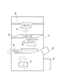
図1は、本発明の実施の形態によるスパッタ装置の正面断面図であり、図2は、平面断面図である。
【0026】
図1及び図2に示す実施形態のスパッタ装置の基本構成は、真空チャンバー1を排気する排気系2、スパッタプロセスガスを供給するガス供給系3と複数のカソードにスパッタ電力を供給する電源4で構成されている。電源4は、カソード毎に電源が接続されていてもよいし、1台の電源で切り替え器を用い使用するカソードのみに電力を供給するタイプでも良い。真空チャンバー内部には、複数のターゲットが取り付けられたカソードユニット5と基体6を回転保持しながらスキャンするスキャンユニット7で構成されている。
更に、チャンバー内部を詳しく説明すると、カソードユニット5はチャンバー1の上面及び底面から磁気シール8,9を介してカソード回転軸10,11で固定され、磁気シール9の下部にはカソード駆動系12が配設されている。多角柱のカソードユニット5の側面には、電気的に絶縁された複数のカソード13a、b、c、dが配設され、異材料のターゲット14a、b、c、dが取り付けられている。又、各カソードにはシャッター15a、b、c、dが配設され独立に開閉できる。回転軸10、11は中空になっていて、その内部には、カソード冷却水や、スパッタ電力供給ケーブルやスパッタリングガス、シャッター駆動用エアー等を供給している。この様な構成にすることで所望のターゲットをスパッタしながら回転移動が可能となる。更に、カソード駆動系12の駆動モーターをサーボモーターを用いることで高精度に位置制御しながら成膜が可能となる。
【0027】
スキャンユニット7は、基体6を保持する基板ホルダー16が基板回転軸17の先端に固定されている。この回転軸17は磁気シール18を介して基板回転させる基板回転駆動系19と、T−Sベローズ20で大気と隔離しながらターゲット基板間距離を可変させるT−S駆動系21と、大気と隔離しながら曲げが可能なSθベローズ22の中心部分に回転中心を持ちユニット全体をチャンバー底面と平行に首振り走査させるスキャン駆動系23で構成させている。この様な構成にすることでスパッタ中に基板回転しながらターゲット基板間距離を可変しながらスキャンして成膜することが可能となる。更に前記のカソード駆動系と同様に各制御軸の駆動モーターをサーボモーターにすることで高精度に位置制御しながら成膜が可能となる。
【0028】
チャンバー内部の各ユニットの配置関係は、カソードユニット7の回転軸をY軸とし、ターゲット14の中心を通るチャンバー底面に平行な軸をX、Z軸とすると、基板回転軸17はX軸に対しZ軸方向にオフセットしたX’軸上に基板回転軸を有し、更にスキャン軸はX’軸上に回転中心を有しスキャンユニット全体をXZ面上のスキャン動作をする。
【0029】
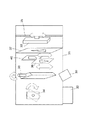
図8は、本発明の別の実施の形態によるスパッタ装置の断面図である。
【0030】
図8に示す実施形態のスパッタ装置の基本構成は、真空チャンバー31を排気する排気系32、回転するスパッタリングターゲツト4がある。また、基体3を回転保持しながらスキャンするスキャンユニット35がある。基板とターゲットの間には、成膜領域を変えるための可動マスク36と固定マスク37を有し、成膜粒子の方向およびレートを決めるコリメータ38がある。このコリメータは回転可能になっており、この角度を変えることにより、成膜レートを可変できる。
【0031】
スパッタリングは、イオン源を用いたイオンビームスパッタでも、ターゲットに電力を供給するマグネトロンスパッタ方式でもどちらでも良い。
【0032】
【実施例】
(実施例1)
本発明のスパッタ装置を用いた実際の多層成膜は、下記の手順で行われる。
スキャン条件設定
スキャン条件の待機時間又は移動速度の最適化
【0033】
成膜工程
▲1▼のスキャン条件設定は、本スパッタ装置のCAD図面の平面図を用いて各ステップ条件のターゲット角度Tθ、T-S間距離、スキャン軸角度Sθを求める方法とプログラムを作成してT-S間距離が一定でターゲット中心と基板上の各ステップを結ぶ線の各交点上の法線との角度sin(tθ)2+sin(sθ)2が最小となる最適化計算によるTθ、Sθ条件を求める方法がある。本実施例では、CAD図面から求める方法で説明する。
まず、CAD図面上で基板ホルダーに取り付けられたレンズの半径よりも約2割程度大きさの半径方向を10〜20分割し、その分割された点をレンズ中心からP0、P1、P2・・・P20とする。ターゲット中心とレンズ表面上のP0、P1、・・・・P20の各T-S間距離を100mmに一定にしてレンズ表面上のP0、P1、・・・・P20の法線とターゲット中心の法線がほぼ一致する各ターゲット角度Tθと各スキャン軸角度Sθを求める。
【0034】
▲2▼上記▲1▼で求めた各ポイントのターゲット角度Tθ、T-S間距離、スキャン軸角度Sθ条件で膜厚分布シミュレーションを用いそれぞれのターゲット材の膜厚分布を算出する。算出した各ポイントの膜厚分布に待機時間を掛けた合計が所望の膜厚分布となる様に最小二乗法を用いて待機時間を最適化する。
【0035】
▲3▼成膜工程では、上記の各ターゲット材料の最適化条件の成膜速度から所望の膜厚となる様に各ポイントの待機時間をスパッタ装置に入力する。次に最適化条件された形状のレンズを基板ホルダーに取り付けロードロック室を介して真空チャンバー内のスキャンユニットにセットする。
【0036】
真空チャンバー内を排気ユニットで十分に排気後、設定された各ポイントのターゲット角度Tθ、T-S間距離、スキャン軸角度Sθ条件で最適化された待機時間で成膜を開始する。
【0037】
成膜後、この基板を取り出し膜厚分布を計測した結果、所望の膜厚分布が得られなかった場合、そのずれ量を補正した待機時間の最適化を行えば容易に所望の膜厚分布を得ることが出来る。
【0038】
(実施例2)
実施例1と同様の構成で各ステップの膜厚シミュレーション結果で得られた所望の膜厚分布となる最適条件からターゲット角度Tθ、T-S間距離、スキャン軸角度Sθの各移動速度を連続的に可変して条件設定しても実施例1と同様の効果が得られる。
【0039】
次に凹凸基板の膜厚分布制御性比較として基体を蒸発源に対し平行なX又はXY方向に移動しながら成膜する方法(特許文献2)と本発明であるターゲット角度Tθ、T-S間距離、スキャン軸角度Sθを制御した方式の比較シミュレーションを行った。
ターゲットはφ5インチ、T-S間距離100、120、150mm、基板中心から半径方向に15mmピッチで16ステップ移動、基板は外径φ300mmで曲率300mmの凸形状基板で回転動作している形態で成膜圧力は散乱の影響が少なくなる放電維持限界0.1Pa程度を想定して散乱効果は無視した。更に放出角度分布は余弦則で計算した。
【0040】
図3は上記凸レンズを蒸発源に対し平行なX方向に15mmピッチで16ステップ移動した従来例方式の場合の各ステップにおける膜厚分布を表したものである。この各ステップの膜厚分布及び成膜速度に待機時間の積の和が所望の100%(全体が均一な膜厚分布)と115%(レンズ中心から周辺に向かって直線的に115%迄増加する)の膜厚分布になる様に待機時間を最適化して求めた膜厚分布が図4である。
【0041】
図5は本発明の構成でシミュレーション計算した各ステップの膜厚分布を示したもので、基本条件は前記と同じであるがターゲット角度Tθ、スキャン軸角度Sθ、及びT−S間距離をCAD図面から求めた。レンズの半径方向を16分割し、その分割された点をレンズ中心からP0、P1、P2・・・P15とします。T-S間距離を100、120、150mmに一定にしてレンズP0、P1、・・・・P10の法線とターゲット中心の法線がほぼ一致する各ターゲット角度Tθと各スキャン軸角度Sθを求めた値を用いた。
【0042】
図6は上記同様に、図5の各ステップの膜厚分布及び成膜速度に待機時間の積の和が100%(全体が均一な膜厚分布)と115%(レンズ中心から周辺に向かって直線的に115%迄増加する)の膜厚分布になる様に待機時間を最適化して求めたものである。
【0043】
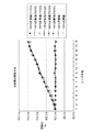
又、図7は全体の待機時間に対する各ステップに於ける待機時間を比率で表した表である。図3、5及び図7でわかるように従来方式では、レンズ外周部の膜厚はスパッタ粒子の基板への斜入射成分が多い点とTS間距離が大きくなる影響で薄くなり、その結果、外周部を成膜する待機比率が高くなり、更に成膜面積の小さい中心部も同時に成膜されてしまうので膜厚均一性も本発明に比べ悪い。尚、本発明でターゲット前面に中空円柱状のチムニーを設けると更に斜入射成分がカットされより膜厚分布や膜質均一化が図れ更に好ましい。
【0044】
(実施例3)
図9は、本実施例の装置形態である。
図9に示すスパッタ装置の基本構成は、真空チャンバー31を排気する排気系32、回転するスパッタリングターゲット34がある。また、基体33を回転保持しながらスキャンするスキャンユニット35がある。基板とターゲツトとの間には、成膜領域を変えるための可動マスク36と固定マスク37を有し、成膜粒子の方向およびレートを決めるコリメータ38がある。このコリメータは回転可能になっており、この角度を変えることにより、成膜レートを可変できる。スパッタリングは、イオン源39を用いたイオンビームスパッタ方式である。
【0045】
本装置を用いて、成膜する手順を説明する。
真空チャンバー31に基板33を導入し、10−4Pa以下の圧力まで待機する。その後、基板33を回転し、イオンビーム39とターゲット34を所望の角度にし、成膜開始する。その際、スキャンユニットおよび、可動マスク36を動かし、基板33上の膜厚分布を制御する。また、成膜レートをコリメータ8によって制御し、均一性を高めている。
この装置を用いた結果、±0.2%以下の精度で所望の膜厚を得ることができた。
【0046】
(実施例2)
図10は、本実施例の装置形態である。
図10に示すスパッタ装置の基本構成は、真空チャンバー31を排気する排気系32、回転するスパッタリングターゲット34がある。また、回転放物面形状を持つ基体33をスキャンするスキャンユニット35がある。基板とターゲットの間には、成膜領域を変えるための可動マスク36および40と固定マスク37を有し、成膜粒子の方向およびレートを決めるコリメータ38がある。このコリメータは回転可能になっており、この角度を変えることにより、成膜レートを可変できる。スパッタリングは、イオン源39を用いたイオンビームスパッタ方式である。
【0047】
本装置を用いて、成膜する手順を説明する。
真空チャンバー31に基板3を導入し、10−4Pa以下の圧力まで待機する。その後、基板33を回転し、イオンビーム39とターゲット34を所望の角度にし、成膜開始する。その際、スキャンユニットおよび、可動マスク36および37を動かし、基板33上の膜厚分布を制御する。また、成膜レートをコリメータ38によって制御し、均一性を高めている。
この装置を用いた結果、±0.2%以下の精度で所望の膜厚を得ることができた。
【0048】
ここで、以下に本発明の実施態様を示す。
(実施態様1) 凹凸又は平面形状を有する基板に物理的気相成長にて膜を成膜するスパッタ装置に於いて、成膜中に基板とカソードの相対位置関係等を独立に可変出来る制御軸が3軸以上有することを特徴とするスパッタ装置。
(実施態様2) 前記基板とカソードの相対位置関係等を独立に可変出来る少なくとも3個の制御軸は、基板を回転する軸と、1または2以上のカソードで構成されたカソード回転軸と、回転する基板を走査するスキャン軸と、であることを特徴とする実施態様1に記載のスパッタ装置。
(実施態様3) 前記カソード回転軸はターゲット面に平行なY軸上で、Z軸にオフセットされたX’軸上に回転中心を持ちXZ面上に走査するスキャン軸と、スキャン軸でXZ面上を移動するユニット内に組み込まれた基板を回転する回転軸と、を有する配置関係であることを特徴とする実施態様2に記載のスパッタ装置。
【0049】
上記実施態様1ないし3のいずれかによれば、 いろいろな形状の基体に光学薄膜を均質且つ高精度に所望の膜厚分布を得ることができる。
(実施態様4) 前記基板とカソードとの相対位置関係等を独立に可変制御出来るカソード対面側に配置された基板を回転する軸と、1又2以上のカソードで構成されたカソード回転軸と、回転する基板を走査するスキャン軸の3軸と、更にターゲット基板間の距離を可変可能なTS制御軸と、を有することを特徴とする実施態様2に記載のスパッタ装置。
(実施態様5) 前記カソード回転軸は、さらに、ターゲット基板間距離を可変するTS制御軸を有する配置関係であることを特徴とする実施態様2または4のスパッタ装置。
【0050】
上記実施態様4または5によれば、ターゲットレンズ間の距離が一定となる様に制御しながら前記の様なスキャン成膜を行えば成膜条件が同一となり均質な膜を得ながら膜厚分布の制御が可能となる。
(実施態様6) 実施態様1ないし5のいずれかに記載のスパッタ装置において、カソード回転軸と基板回転軸とスキャン軸とTS軸制御軸の内少なくとも2軸以上の制御された複数条件の移動速度を1回又は複数回繰り返しスキャンして成膜することを特徴とするスパッタ成膜方法。
(実施態様7) 前記カソード回転軸と基板回転軸とスキャン軸とTS制御軸の内少なくとも2軸以上の制御された複数条件位置の滞在時間を1回又は複数回繰り返しスキャンして成膜することを特徴とする実施態様6に記載のスパッタ成膜方法。
【0051】
上記実施態様6または7によれば、スパッタ粒子の垂直入射成分を多く含んだ膜で且つ所望の膜厚分布を得ることが出来る。同様に、前記複数条件を連続に可変してその2軸の可変速度を制御しながら1回もしくは複数回スキャンすることでも同様の効果を得る事ができる。
(実施態様8) 自由な曲面形状を有する基板に物理的気相成長にて膜を成膜するスパッタ装置であり、成膜中に基板とカソードの相対位置関係を独立に可変出来る制御軸を3軸以上有することを特徴とするスパッタ装置において、相対位置関係の制御軸とは独立に成膜中にレートまたは成膜領域、またはその両方を可変できる機能を1つ以上備えたことを特徴とするスパッタ装置。
(実施態様9) 前記成膜中にレートまたは成膜領域、またはその両方を可変できる機能とは、可動型のマスクであることを特徴とする実施態様8に記載のスパッタ装置。
(実施態様10) 前記成膜中にレートまたは成膜領域、またはその両方を可変できる機能とは、コリメータの角度を変え、開口率を制御することであることを特徴とする実施態様8に記載のスパッタ装置。
(実施態様11) 実施態様9及び10に記載のスパッタ装置において、前記成膜中にレートまたは成膜領域、またはその両方を可変できる機能とは、前記可動型のマスクとコリメータの角度を変え、開口率を制御する複数の機能を組み合わせていることを特徴とする実施態様8に記載のスパッタ装置。
(実施態様12) 実施態様8に記載のスパッタ装置において、前記基板とカソードの相対位置関係等を独立に可変出来る3個以上の制御軸の一つは、基板を走査する軸であり、かつその走査軸と連動して成膜中にレートまたは成膜領域、またはその両方を可変できる機能を1つ以上備えたことを特徴とする実施態様8ないし11のいずれかに記載のスパッタ装置。
(実施態様13) 前記基板を走査する軸とは、直線的に走査するスキャン軸であることを特徴とする実施態様12に記載のスパッタ装置。
【0052】
上記実施態様8ないし13のいずれかによれば、レンズ、ミラー等の様々な形状を有する高性能な光学部品を基板とする成膜プロセスにおいて、成膜中にレートまたは成膜領域、またはその両方を可変できる機能を付加することにより、所望の膜厚分布を有する成膜を効率的に行なうことができる。
【0053】
【発明の効果】
本発明は上述のとおり構成されているスパッタ装置及び成膜方法なので、以下に記載するような効果を奏する。
【0054】
レンズ等の凹凸形状を有する高性能な光学部品を基板とする成膜プロセスにおいて、各ステップのターゲット角度Tθ、スキャン軸角度Sθ条件を最適化してスパッタ粒子の垂直入射成分を主とした部分成膜領域を走査速度制御された連続又は待機時間制御されたステップスキャン走査することでレンズ面内に膜密度の高い均質膜が得られ且つ所望の膜厚分布を有する反射防止膜等の成膜を効率的に行なうことができる。
【0055】
さらに、レンズ、ミラー等の様々な形状を有する高性能な光学部品を基板とする成膜プロセスにおいて、成膜中にレートまたは成膜領域、またはその両方を可変できる機能を付加することにより、所望の膜厚分布を有する成膜を効率的に行なうことができる。
【図面の簡単な説明】
【図1】本発明の実施の形態によるスパッタ装置の正面断面図である。
【図2】本発明の実施の形態によるスパッタ装置の平面断面図である。
【図3】従来方式の各ステップに於ける膜厚分布(φ300、凸形状、曲率300レンズ)である。
【図4】従来方式の各ステップの待機時間を最適化したときの膜厚分布(φ300、凸形状、曲率300レンズ)である。
【図5】本発明の各ステップに於ける膜厚分布(φ300、凸形状、曲率300レンズ)である。
【図6】本発明の各ステップの待機時間を最適化したときの膜厚分布(φ300、凸形状、曲率300レンズ)である。
【図7】最適化した時の待機時間である。
【図8】本発明の別の実施の形態によるスパッタ装置の概略図である。
【図9】本発明の実施例3の形態によるスパッタ装置の概略図である。
【図10】本発明の実施例4の形態によるスパッタ装置の概略図である。
【符号の説明】
1 真空チャンバー、
2 排気系、
3 スパッタプロセスガスを供給するガス供給系、
4 スパッタ電力を供給する電源、
5 複数のターゲットが取り付けられたカソードユニット、
6 基体、
7 スキャンユニット、
8,9 磁気シール、
10,11 カソード回転軸、
12 カソード駆動系、
13a,b,c,d カソード、
14a,b,c,d ターゲット、
15a,b,c,d シャッター、
16 基板ホルダー、
17 基板回転軸、
18 磁気シール、
19 基板回転させる基板回転駆動系、
20 T−Sベローズ、
21 ターゲット基板間距離を可変させるT−S駆動系、
22 Sθベローズ、
23 スキャン駆動系、
31 真空チャンバー、
32 排気系、
33 基体、
34 ターゲット
35 スキャンユニット、
36 可動マスク、
37 固定マスク、
38 開口率および開口方向調整板(コリメータ)、
39 イオンガン、
40 可変マスク。[0001]
BACKGROUND OF THE INVENTION
The present invention relates to a sputtering apparatus and a sputtering method for forming a film with a desired film thickness distribution and a uniform film thickness distribution characteristic when forming a film on a substrate having an uneven shape attached to a substrate holder. The present invention relates to a film formation apparatus and a film formation method for a multilayer antireflection film, a multilayer film mirror, and an X-ray reflection multilayer film having a desired film thickness distribution on a substrate such as a large aperture lens.
[0002]
[Prior art]
Parallel plate magnetron sputtering, which has been widely used in the past, generates plasma after placing a target, which is a thin film material, and a substrate attached to a substrate holder in a vacuum chamber so as to face each other. The target is sputtered and the sputtering particles knocked out by sputtering are deposited on the substrate to form a thin film on the substrate. It is characterized by excellent target life.
[0003]
In recent years, such sputtering devices have been studied for sputtering in the field of optical films. In particular, semiconductor exposure printing devices such as steppers have been used to increase the NA in order to improve the printing performance, and to increase the lens diameter and lens. There is a demand for an improved oblique incidence characteristic of incident light, and for a next-generation X-ray (EUV) exposure apparatus such as a large-diameter and high-precision inclined film (improvement of oblique incidence characteristic).
[0004]
Molybdenum (Mo) and silicon (Si) X-ray multilayer mirrors using an X-ray wavelength of 13.4 nm have a very narrow bandwidth for reflection characteristics, so that the reflection characteristics vary depending on the incident angle of X-rays incident on the mirror surface. Decreases. As an improvement measure, a method is adopted in which the reflection mirror characteristics are adapted to the X-ray incident angle in the reflection mirror surface. Therefore, it is necessary to control the film thickness distribution of molybdenum (Mo) and silicon (Si) with high accuracy in the reflection mirror surface.
[0005]
As a method of controlling the film thickness distribution, a method of controlling the film thickness distribution by using a shielding mask and controlling the shape and moving speed distribution of the shielding mask (Patent Document 1), or an X parallel to the evaporation source Alternatively, a method of forming a film while moving in the XY direction (Patent Document 2) Further, an inclined film forming method (Patent Document 3) is proposed by controlling the revolving speed when a substrate that rotates and revolves over a target. Yes.
[0006]
However, optical elements used in exposure apparatuses and the like are diversified because there are shortened wavelengths and shapes are different from aspheric surfaces, free-form surfaces, paraboloids, and the like. Therefore, more accurate film thickness control is required than before.
[0007]
As described above, in order to realize an optical element that requires very high precision film thickness distribution control, the following film forming apparatus and film forming method are required.
(1) Film thickness distribution control is possible for various uneven shapes
(2) Capable of responding to multiple targets (thickness distributions differ due to differences in material release angle distribution).
(3) Since the oblique incidence film of sputtered particles has a low film density, the refractive index changes due to moisture adsorption and the optical characteristics change. Therefore, the film forming apparatus must suppress the oblique incidence component of the sputtered particles as much as possible.
(4) A load-lock type film formation is possible to suppress the generation of dust and residual gas, particularly water, as much as possible.
(5) The film forming apparatus does not introduce a complicated moving mechanism in the vacuum apparatus.
[0008]
In the method (Patent Document 1) for controlling the film thickness distribution by controlling the shape and moving speed distribution of the shielding mask using the shielding mask described above, one shape is required to satisfy the above (1) and (2). It is difficult to cope with the mask, and it is necessary to open the vacuum chamber to the atmosphere and replace the mask. When the vacuum chamber is opened to the atmosphere, water in the atmosphere is adsorbed on the film adhering to the vacuum chamber, the film stress increases, and the film is liable to be peeled off. Further, since a shielding mask is installed in the vicinity of the base between the target and the base, it is not preferable because it becomes a dust generation source.
[0009]
Furthermore, in the method of controlling the film thickness distribution by using the above-described shielding mask and controlling the shape and moving speed distribution of the shielding mask (Patent Document 1), only a rotationally symmetric film can be attached. Can not respond. Similarly, only a rotationally symmetric film can be formed by the method of forming a tilted film by controlling the revolving speed when a substrate that rotates and revolves over the target (Patent Document 3).
[0010]
Also, a method of forming a film while moving the substrate in the X or XY direction parallel to the evaporation source
According to
[Patent Document 1]
Japanese Patent Laid-Open No. 10-30170
[Patent Document 2]
JP-A-9-213634
[Patent Document 3]
USP 6010600 Specification
[0011]
[Problems to be solved by the invention]
An object of the present invention is to obtain a desired film thickness distribution with high accuracy and a uniform optical thin film on a substrate having various shapes by a method different from the conventional method.
[0012]
[Means for Solving the Problems]
In order to achieve the above object, a sputtering apparatus and a sputtering method of the present invention are sputtering apparatuses for forming a film on a substrate having irregularities or a planar shape by physical vapor deposition, wherein the substrate and the target are formed during the film formation. There are three or more control axes that can independently move and scan the relative positional relationship.
The three axes capable of independently controlling the relative positional relationship between the substrate and the target are an axis for rotating the substrate, a cathode rotation axis composed of at least one or a plurality of cathodes, and a scan for scanning the rotating substrate. Is the axis.
[0013]
When the arrangement relation of the three control axes is expressed in an XYZ solid diagram (see FIGS. 1 and 2), the cathode rotation axis is on the Y axis parallel to the target surface, and the rotation center is on the X ′ axis offset to the Z axis. And a scanning axis that scans on the XZ plane and a rotation axis that rotates the substrate incorporated in the unit that moves on the XZ plane with the scanning axis.
[0014]
Furthermore, there are a total of four axes, the above three axes and the TS axis capable of changing the distance between the target and the substrate.
When the arrangement of the four control axes is expressed in an XYZ solid diagram, the cathode rotation axis is on the Y axis parallel to the target surface and has a rotation center on the X ′ axis offset to the Z axis and on the XZ surface. This is achieved by the above-described means having a scan axis for scanning, a rotation axis for rotating a substrate incorporated in a unit moving on the XZ plane with the scan axis, and a TS control axis for changing the distance between the target substrates. .
[0015]
Further, the film forming method of the present invention is such that the moving speed under a plurality of controlled conditions of at least two or more of the cathode rotation axis, the substrate rotation axis, the scan axis, and the TS control axis in the above sputtering apparatus is set once or a plurality of times. This is accomplished by a method of repeatedly forming a film by scanning, or a method of forming a film by repeatedly scanning the stay time at a plurality of controlled positions of two or more axes once or a plurality of times.
[0016]
The sputtering apparatus of the present invention is a sputtering apparatus that forms a film on a substrate having various shapes by physical vapor deposition, and independently moves and scans the relative positional relationship between the substrate and the target during the film formation. There are three or more control axes that can be used, and a mechanism that can freely control the film formation rate and film formation region.
[0017]
One of the three sleeves that can control the relative positional relationship between the substrate and the target independently is a scan axis for scanning the substrate.
[0018]
The mechanism capable of freely controlling the film formation rate and the film formation region is a movable mask and a movable collimator.
[0019]
The film forming method of the present invention is achieved by forming a free film thickness distribution on a substrate having various shapes by controlling the mask and / or collimator in synchronization with other axes in the sputtering apparatus. Is done.
[0020]
[Action]
The configuration of the present invention is such that the cathode rotation axis composed of at least one or a plurality of cathodes (when the arrangement relation is expressed in an XYZ three-dimensional view) is X ′ offset on the Z axis on the Y axis parallel to the target surface. A scan axis that has a rotation center on the axis and scans on the XZ plane, and a rotation axis that rotates the substrate incorporated in the unit that moves on the XZ plane by the scan axis and a TS control axis that varies the distance between the target substrates . When a concave / convex surface-shaped substrate is set in the substrate holder with this configuration, for example, when a convex lens having an outer diameter of φ300 mm and a radius of curvature R = 300 mm is set on the rotating substrate holder, the rotated lens is on the XZ plane. In addition, the XZ axis has a rotation center on the cathode rotation angle (Tθ) and the X ′ axis offset to the Z axis so that the lens normal line is almost perpendicular to the target film formation surface in any film formation region of the target side radius. This can be achieved by the biaxial angle of the scan axis angle (Sθ) for scanning on the surface.
[0021]
In this way, multiple conditions where the target and the film formation area in the lens face each other are set, and film formation is performed while scanning one or more times while controlling the staying time of the conditions, so that a lot of normal incident components of sputtered particles are included. A desired film thickness distribution can be obtained with a thick film. Similarly, the same effect can be obtained by continuously changing the plurality of conditions and scanning one or more times while controlling the variable speeds of the two axes.
[0022]
Furthermore, by adding a TS control axis that can change the distance between the target and the substrate, the film forming conditions are the same if the scan film is formed as described above while controlling the distance between the target lenses to be constant. It is more preferable because the film thickness distribution can be controlled while obtaining a homogeneous film.
(While the above-described operation has been described with a convex lens, the cathode rotation angle (Tθ), the scan axis angle (Sθ), even if the emission angle distribution of sputtered particles changes when the concave lens or target material is switched to a different material. (The same effect can be obtained by optimizing the distance between the target and the substrate.)
Further, the above configuration requires a slightly complicated operation in the vacuum atmosphere of the film forming chamber of the sputtering apparatus having a load lock chamber. In the present invention, a magnetic seal is used for the target rotating shaft and the substrate rotating shaft. The rotation axis, the scan axis uses a system that covers the periphery of the rotation center with a bellows, and the TS axis that can change the distance between the target and the substrate is a highly reliable mechanism that does not easily generate leaks etc. due to the movement mechanism using the bellows The mechanism was relatively easy to obtain.
[0023]
Therefore, in the conventional mask moving method and the method of moving the substrate in the X and Y axis parallel methods, the film density of the oblique incident component of the sputtered particles is large in the peripheral region of the lens in the film formation of the uneven substrate. However, in the sputtering apparatus of the present invention, the cathode rotation angle (Tθ), the scan axis angle (Sθ), and the distance between the target and the substrate even if the emission angle distribution and the substrate shape (unevenness) due to the target material change. By optimizing the distance condition, it was possible to obtain a lens having a desired film thickness distribution that is homogeneous and highly accurate throughout the lens.
[0024]
DETAILED DESCRIPTION OF THE INVENTION
Embodiments of the present invention will be described with reference to the drawings.
[0025]
FIG. 1 is a front sectional view of a sputtering apparatus according to an embodiment of the present invention, and FIG. 2 is a plan sectional view.
[0026]
The basic configuration of the sputtering apparatus of the embodiment shown in FIGS. 1 and 2 includes an
Further, the interior of the chamber will be described in detail. The
[0027]
In the
[0028]
The arrangement of the units inside the chamber is such that the rotation axis of the
[0029]
FIG. 8 is a cross-sectional view of a sputtering apparatus according to another embodiment of the present invention.
[0030]
The basic configuration of the sputtering apparatus of the embodiment shown in FIG. 8 includes an
[0031]
Sputtering may be either ion beam sputtering using an ion source or magnetron sputtering that supplies power to a target.
[0032]
【Example】
Example 1
The actual multilayer film formation using the sputtering apparatus of the present invention is performed according to the following procedure.
Scan condition setting
Optimization of waiting time or moving speed of scanning conditions
[0033]
Film formation process
The scan condition setting of (1) is a method and program for determining the target angle Tθ, the distance between TSs, and the scan axis angle Sθ of each step condition using the plan view of the CAD drawing of this sputtering apparatus. An angle sin (tθ) between the target center and the normal on each intersection of the line connecting each step on the substrate2+ Sin (sθ)2There is a method for obtaining the Tθ and Sθ conditions by optimization calculation that minimizes. In the present embodiment, a description will be given by a method obtained from a CAD drawing.
First, in the CAD drawing, the radial direction that is about 20% larger than the radius of the lens attached to the substrate holder is divided into 10 to 20, and the divided points are P0, P1, P2,. P20. P0, P1,... P20 on the lens surface and the T-S distance of P20 are set to 100 mm, and the normals of P0, P1,. Each target angle Tθ and each scan axis angle Sθ in which the lines substantially coincide are obtained.
[0034]
(2) The film thickness distribution of each target material is calculated using the film thickness distribution simulation under the conditions of the target angle Tθ, the distance between TS and the scan axis angle Sθ at each point obtained in (1) above. The standby time is optimized using the least square method so that the sum of the calculated film thickness distribution of each point multiplied by the standby time becomes a desired film thickness distribution.
[0035]
{Circle around (3)} In the film forming step, the standby time at each point is input to the sputtering apparatus so as to obtain a desired film thickness from the film forming speed under the optimization conditions of each target material. Next, the lens having the optimized shape is attached to the substrate holder and set in the scan unit in the vacuum chamber via the load lock chamber.
[0036]
After the inside of the vacuum chamber is sufficiently evacuated by the evacuation unit, the film formation is started with the standby time optimized based on the target angle Tθ, the distance between TS and the scan axis angle Sθ at the set points.
[0037]
After film formation, this substrate is taken out and the film thickness distribution is measured. As a result, if the desired film thickness distribution is not obtained, the desired film thickness distribution can be easily obtained by optimizing the standby time by correcting the deviation amount. Can be obtained.
[0038]
(Example 2)
The moving speeds of the target angle Tθ, the distance between TSs, and the scan axis angle Sθ are continuously variable from the optimum conditions that achieve the desired film thickness distribution obtained from the film thickness simulation results at each step with the same configuration as in the first embodiment. Even if the conditions are set, the same effect as in the first embodiment can be obtained.
[0039]
Next, as a comparison of the film thickness distribution controllability of the concavo-convex substrate, a method of forming a film while moving the substrate in the X or XY direction parallel to the evaporation source (Patent Document 2) and the target angle Tθ, the distance between TS, A comparative simulation of a method in which the scan axis angle Sθ was controlled was performed.
The target is φ5 inch, the distance between TS is 100, 120, 150 mm, moves 16 steps in the radial direction from the substrate center at a pitch of 15 mm, and the substrate is rotated on a convex substrate with an outer diameter of φ300 mm and a curvature of 300 mm. Assumed a discharge maintenance limit of about 0.1 Pa where the influence of scattering was reduced, and the scattering effect was ignored. Furthermore, the emission angle distribution was calculated by the cosine law.
[0040]
FIG. 3 shows the film thickness distribution at each step in the case of the conventional method in which the convex lens is moved by 16 steps at a pitch of 15 mm in the X direction parallel to the evaporation source. The sum of the product of the waiting time and the film thickness distribution and film formation speed of each step increases to the desired 100% (uniform film thickness distribution as a whole) and 115% (from the center of the lens to 115% linearly) FIG. 4 shows the film thickness distribution obtained by optimizing the standby time so as to obtain the film thickness distribution.
[0041]
FIG. 5 shows the film thickness distribution of each step calculated by the simulation of the configuration of the present invention. The basic conditions are the same as above, but the target angle Tθ, the scan axis angle Sθ, and the distance between TS are CAD drawings. I asked for it. Divide the radial direction of the lens into 16, and the divided points are P0, P1, P2, ... P15 from the lens center. The distance between TS is fixed to 100, 120, and 150 mm, and the target angle Tθ and the scan axis angle Sθ at which the normals of the lenses P0, P1,. Values were used.
[0042]
In FIG. 6, as in the above, the sum of the product of the film thickness distribution and the film formation speed of each step of FIG. 5 and the waiting time is 100% (uniform film thickness distribution as a whole) and 115% (from the lens center toward the periphery). The waiting time is optimized so as to obtain a film thickness distribution that increases linearly to 115%.
[0043]
FIG. 7 is a table showing the ratio of the waiting time at each step to the entire waiting time. As can be seen from FIGS. 3, 5 and 7, in the conventional method, the film thickness at the outer periphery of the lens becomes thinner due to the fact that the oblique incident component of the sputtered particles on the substrate is large and the distance between TSs is increased. The standby ratio for forming the film is increased, and the central part having a small film formation area is also formed at the same time. In the present invention, it is more preferable to provide a hollow cylindrical chimney on the front surface of the target because the oblique incident component is further cut and the film thickness distribution and film quality can be made uniform.
[0044]
(Example 3)
FIG. 9 shows an apparatus configuration of this embodiment.
The basic configuration of the sputtering apparatus shown in FIG. 9 includes an
[0045]
A procedure for forming a film using this apparatus will be described.
The
As a result of using this apparatus, a desired film thickness could be obtained with an accuracy of ± 0.2% or less.
[0046]
(Example 2)
FIG. 10 shows an apparatus configuration of this embodiment.
The basic configuration of the sputtering apparatus shown in FIG. 10 includes an
[0047]
A procedure for forming a film using this apparatus will be described.
The
As a result of using this apparatus, a desired film thickness could be obtained with an accuracy of ± 0.2% or less.
[0048]
Here, embodiments of the present invention will be described below.
(Embodiment 1) In a sputtering apparatus for forming a film on a substrate having irregularities or a planar shape by physical vapor deposition, a control axis capable of independently changing the relative positional relationship between the substrate and the cathode during the film formation. Has three axes or more.
(Embodiment 2) At least three control shafts capable of independently changing the relative positional relationship and the like of the substrate and the cathode include a shaft for rotating the substrate, a cathode rotating shaft composed of one or more cathodes, and a rotation And a scanning axis for scanning a substrate to be sputtered.
(Embodiment 3) The cathode rotation axis is a Y axis parallel to the target plane, a scan axis having a rotation center on the X ′ axis offset to the Z axis and scanning on the XZ plane, and an XZ plane as the scan axis The sputtering apparatus according to
[0049]
According to any of the
(Embodiment 4) A shaft for rotating a substrate disposed on the cathode facing side capable of independently and variably controlling the relative positional relationship between the substrate and the cathode, a cathode rotating shaft composed of one or more cathodes, 3. The sputtering apparatus according to
(Embodiment 5) The sputtering apparatus according to
[0050]
According to the
(Embodiment 6) In the sputtering apparatus according to any one of
(Embodiment 7) Film formation is performed by repeatedly scanning the residence time at a plurality of controlled condition positions of at least two of the cathode rotation axis, the substrate rotation axis, the scan axis, and the TS control axis once or a plurality of times. The sputter film-forming method of
[0051]
According to the
(Embodiment 8) A sputtering apparatus that forms a film on a substrate having a free curved surface by physical vapor deposition, and has 3 control axes capable of independently changing the relative positional relationship between the substrate and the cathode during film formation. A sputtering apparatus characterized by having at least an axis includes at least one function capable of changing a rate and / or a film forming area during film formation independently of a relative positional control axis. Sputtering device.
(Embodiment 9) The sputtering apparatus according to
(Embodiment 10)
(Embodiment 11) In the sputtering apparatus according to
(Embodiment 12) In the sputtering apparatus according to
(Embodiment 13) The sputtering apparatus according to
[0052]
According to any one of the
[0053]
【The invention's effect】
Since the present invention is a sputtering apparatus and film forming method configured as described above, the following effects can be obtained.
[0054]
In a film-forming process using a high-performance optical component having a concavo-convex shape such as a lens as a substrate, partial film formation mainly using a normal incidence component of sputtered particles by optimizing the target angle Tθ and scan axis angle Sθ conditions of each step A uniform film with a high film density can be obtained in the lens plane by scanning the area continuously or with a scanning time controlled step-by-step controlled scan time. Can be done automatically.
[0055]
Furthermore, in a film forming process using a high-performance optical component having various shapes such as a lens and a mirror as a substrate, a function capable of changing a rate and / or a film forming region during film forming is added, thereby adding a desired function. It is possible to efficiently perform the film formation having the film thickness distribution.
[Brief description of the drawings]
FIG. 1 is a front sectional view of a sputtering apparatus according to an embodiment of the present invention.
FIG. 2 is a plan sectional view of a sputtering apparatus according to an embodiment of the present invention.
FIG. 3 is a film thickness distribution (φ300, convex shape, curvature 300 lens) in each step of the conventional method.
FIG. 4 is a film thickness distribution (φ300, convex shape, curvature 300 lens) when the standby time of each step of the conventional method is optimized.
FIG. 5 is a film thickness distribution (φ300, convex shape, curvature 300 lens) in each step of the present invention.
FIG. 6 is a film thickness distribution (φ300, convex shape, curvature 300 lens) when the standby time of each step of the present invention is optimized.
FIG. 7 is a waiting time when optimized.
FIG. 8 is a schematic view of a sputtering apparatus according to another embodiment of the present invention.
FIG. 9 is a schematic view of a sputtering apparatus according to a mode of Example 3 of the present invention.
FIG. 10 is a schematic view of a sputtering apparatus according to a mode of Example 4 of the present invention.
[Explanation of symbols]
1 vacuum chamber,
2 exhaust system,
3 Gas supply system for supplying sputtering process gas,
4 Power supply for supplying sputtering power,
5 Cathode unit with multiple targets attached,
6 substrate,
7 Scan unit,
8,9 Magnetic seal,
10,11 Cathode rotating shaft,
12 Cathode drive system,
13a, b, c, d cathode,
14a, b, c, d target,
15a, b, c, d shutter,
16 Substrate holder,
17 substrate rotation axis,
18 Magnetic seal,
19 Substrate rotation drive system for rotating the substrate,
20 T-S bellows,
21 TS drive system for varying the distance between target substrates,
22 Sθ Bellows,
23 Scan drive system,
31 vacuum chamber,
32 Exhaust system,
33 substrate,
34 Target
35 scan units,
36 Movable mask,
37 fixed mask,
38 Opening ratio and opening direction adjustment plate (collimator),
39 Ion Gun,
40 Variable mask.
Claims (7)
前記真空チャンバーの内部に配置されターゲットを保持し、第1の回転軸を有し、該第1の回転軸を中心に前記ターゲットと前記基板が対向するように回転する第1の駆動手段によって回転するカソードユニットと、前記真空チャンバーの内部に配置され、前記基板を前記ターゲットに対向するように保持する基板保持ユニットとを有しており、
前記基板保持ユニットは第2の回転軸を有し、該第2の回転軸を中心に前記基板を軸回転する第2の駆動手段と、前記第2の回転軸上に回転中心を持つ第3の回転軸を有し、前記第3の回転軸を中心に前記基板を首振り走査する第2の駆動手段とを有していて、スパッタの際に、基板表面上の複数点のいずれかの法線とターゲット中心の法線とが一致するように前記カソードユニットの第1の回転軸と基板保持ユニットの第3の回転軸とが、一方の回転軸の回転に連動して他方の回転軸が回転する機構と、前記基板保持ユニットは、前記基板を前記X軸方向に駆動することで、前記基板と前記ターゲットとの距離をスパッタの際に一定に調整する第4の駆動手段を備えていることを特徴とするスパッタ装置。In a sputtering apparatus for forming a film on a substrate having an uneven shape by physical vapor deposition in a vacuum chamber,
Rotated by first driving means disposed inside the vacuum chamber, holding a target, having a first rotation axis, and rotating about the first rotation axis so that the target and the substrate face each other. A cathode unit that is disposed inside the vacuum chamber, and a substrate holding unit that holds the substrate so as to face the target,
The substrate holding unit has a second rotation axis, a second driving means for rotating the substrate about the second rotation axis, and a third having a rotation center on the second rotation axis. And a second driving means for swinging and scanning the substrate about the third rotational axis, and at the time of sputtering, any one of a plurality of points on the substrate surface is provided . The first rotating shaft of the cathode unit and the third rotating shaft of the substrate holding unit are linked with the rotation of one rotating shaft so that the normal line and the normal center of the target coincide with each other. And a fourth driving means for adjusting the distance between the substrate and the target to be constant during sputtering by driving the substrate in the X-axis direction. A sputtering apparatus characterized by comprising:
Priority Applications (2)
| Application Number | Priority Date | Filing Date | Title |
|---|---|---|---|
| JP2003064209A JP4474109B2 (en) | 2003-03-10 | 2003-03-10 | Sputtering equipment |
| US10/795,315 US7229532B2 (en) | 2003-03-10 | 2004-03-09 | Sputtering apparatus |
Applications Claiming Priority (1)
| Application Number | Priority Date | Filing Date | Title |
|---|---|---|---|
| JP2003064209A JP4474109B2 (en) | 2003-03-10 | 2003-03-10 | Sputtering equipment |
Publications (3)
| Publication Number | Publication Date |
|---|---|
| JP2004269988A JP2004269988A (en) | 2004-09-30 |
| JP2004269988A5 JP2004269988A5 (en) | 2006-03-09 |
| JP4474109B2 true JP4474109B2 (en) | 2010-06-02 |
Family
ID=33125553
Family Applications (1)
| Application Number | Title | Priority Date | Filing Date |
|---|---|---|---|
| JP2003064209A Expired - Fee Related JP4474109B2 (en) | 2003-03-10 | 2003-03-10 | Sputtering equipment |
Country Status (2)
| Country | Link |
|---|---|
| US (1) | US7229532B2 (en) |
| JP (1) | JP4474109B2 (en) |
Families Citing this family (27)
| Publication number | Priority date | Publication date | Assignee | Title |
|---|---|---|---|---|
| EP1806425A1 (en) * | 2006-01-09 | 2007-07-11 | Siemens Aktiengesellschaft | Method and apparatus for coating a substrate |
| JP4642789B2 (en) * | 2006-07-14 | 2011-03-02 | セイコーエプソン株式会社 | Film forming apparatus and film forming method |
| CN101490792B (en) * | 2006-07-20 | 2012-02-01 | 阿维扎技术有限公司 | Ion deposition apparatus |
| JP4503098B2 (en) * | 2007-08-29 | 2010-07-14 | キヤノンアネルバ株式会社 | Film formation method and apparatus by sputtering |
| WO2009154009A1 (en) * | 2008-06-20 | 2009-12-23 | キヤノンアネルバ株式会社 | Method for manufacturing magnetoresistive device, sputter film-forming chamber, apparatus for manufacturing magnetoresistive device having sputter film-forming chamber, program and storage medium |
| WO2009157341A1 (en) | 2008-06-25 | 2009-12-30 | キヤノンアネルバ株式会社 | Sputtering device and recording medium whereon a control program thereof is recorded |
| WO2010073323A1 (en) * | 2008-12-24 | 2010-07-01 | キヤノンアネルバ株式会社 | Sputtering apparatus and film forming method |
| US8349143B2 (en) * | 2008-12-30 | 2013-01-08 | Intermolecular, Inc. | Shadow masks for patterned deposition on substrates |
| FR2943072B1 (en) * | 2009-03-12 | 2019-08-16 | Centre National De La Recherche Scientifique Cnrs | MAGNETRON PLASMA SPRAY DECORATION ON GLASS CONTAINERS FOR COSMETIC SECTORS. |
| JP5276121B2 (en) | 2009-06-08 | 2013-08-28 | キヤノンアネルバ株式会社 | Vacuum processing apparatus and optical component manufacturing method |
| US8526104B2 (en) | 2010-04-30 | 2013-09-03 | Corning Incorporated | Plasma ion assisted deposition of Mo/Si multilayer EUV coatings |
| TW201236809A (en) * | 2011-03-01 | 2012-09-16 | Hon Hai Prec Ind Co Ltd | Coating device |
| JP5815743B2 (en) * | 2011-12-28 | 2015-11-17 | キヤノンアネルバ株式会社 | Vacuum processing equipment |
| DE102012205615A1 (en) | 2012-04-04 | 2013-10-10 | Carl Zeiss Smt Gmbh | Coating for producing an optical element having a substrate, whose surface has optically active coating, comprises e.g. placing substrate in substrate plane, generating ions, and deflecting ions moving toward substrate by an electric field |
| JP5921351B2 (en) * | 2012-06-14 | 2016-05-24 | キヤノン株式会社 | Deposition equipment |
| JP2013147752A (en) * | 2013-03-13 | 2013-08-01 | Nippon Dempa Kogyo Co Ltd | Optical element |
| WO2015186732A1 (en) * | 2014-06-03 | 2015-12-10 | シャープ株式会社 | Evaporation apparatus and evaporation method |
| US10541662B2 (en) | 2015-10-14 | 2020-01-21 | Qorvo Us, Inc. | Methods for fabricating acoustic structure with inclined c-axis piezoelectric bulk and crystalline seed layers |
| WO2017106489A2 (en) | 2015-12-15 | 2017-06-22 | Qorvo Us, Inc. | Temperature compensation and operational configuration for bulk acoustic wave resonator devices |
| JP6815153B2 (en) * | 2016-10-03 | 2021-01-20 | 株式会社アルバック | Film deposition equipment |
| DE102016125278A1 (en) * | 2016-12-14 | 2018-06-14 | Schneider Gmbh & Co. Kg | Apparatus, method and use for coating lenses |
| US11824511B2 (en) | 2018-03-21 | 2023-11-21 | Qorvo Us, Inc. | Method for manufacturing piezoelectric bulk layers with tilted c-axis orientation |
| US11381212B2 (en) | 2018-03-21 | 2022-07-05 | Qorvo Us, Inc. | Piezoelectric bulk layers with tilted c-axis orientation and methods for making the same |
| JP7349798B2 (en) | 2019-03-06 | 2023-09-25 | 株式会社タムロン | Anti-reflection film, optical element and anti-reflection film formation method |
| US11401601B2 (en) | 2019-09-13 | 2022-08-02 | Qorvo Us, Inc. | Piezoelectric bulk layers with tilted c-axis orientation and methods for making the same |
| CN112981315A (en) * | 2021-02-05 | 2021-06-18 | 惠州市聚飞光电有限公司 | Black matrix forming method, display module and display device |
| CN115354284A (en) * | 2022-07-15 | 2022-11-18 | 湖南红太阳光电科技有限公司 | Rotating cathode and target base distance online adjusting method |
Family Cites Families (15)
| Publication number | Priority date | Publication date | Assignee | Title |
|---|---|---|---|---|
| JPS6179770A (en) * | 1984-09-28 | 1986-04-23 | Fujitsu Ltd | Device for vapor deposition |
| US4664935A (en) * | 1985-09-24 | 1987-05-12 | Machine Technology, Inc. | Thin film deposition apparatus and method |
| JPS6357759A (en) * | 1986-08-26 | 1988-03-12 | Sumitomo Heavy Ind Ltd | Method and apparatus for surface treatment in vacuum |
| JPS63266061A (en) * | 1987-04-23 | 1988-11-02 | Sumitomo Metal Mining Co Ltd | Producing of multielemental sputtering thin film and sputtering device |
| JPH0774441B2 (en) * | 1987-06-05 | 1995-08-09 | 株式会社日立製作所 | Ion beam spreader device |
| JPH0263534U (en) * | 1988-11-01 | 1990-05-11 | ||
| JPH06219888A (en) * | 1993-01-27 | 1994-08-09 | Sumitomo Metal Mining Co Ltd | Production of oxide crystal producing crucible |
| JP2833979B2 (en) * | 1993-11-26 | 1998-12-09 | 日本電気株式会社 | Sputtering device with collimator |
| JPH0940441A (en) * | 1995-07-26 | 1997-02-10 | Canon Inc | Working device and working method for aspherical lens |
| JPH09213634A (en) | 1996-02-02 | 1997-08-15 | Sony Corp | Thin film-forming method manufacture of semiconductor device and thin film-forming device |
| US6010600A (en) | 1996-02-22 | 2000-01-04 | The Regents Of The University Of California | Maskless deposition technique for the physical vapor deposition of thin film and multilayer coatings with subnanometer precision and accuracy |
| JPH1026698A (en) * | 1996-07-12 | 1998-01-27 | Nikon Corp | Device for forming thin film under vacuum and method for manufacturing reflector |
| JP3861329B2 (en) | 1996-07-17 | 2006-12-20 | 株式会社ニコン | Vacuum thin film forming apparatus and reflector manufacturing method |
| US6086727A (en) * | 1998-06-05 | 2000-07-11 | International Business Machines Corporation | Method and apparatus to improve the properties of ion beam deposited films in an ion beam sputtering system |
| JP2002161365A (en) * | 2000-11-20 | 2002-06-04 | Shimadzu Corp | Apparatus and method for ion beam sputtering |
-
2003
- 2003-03-10 JP JP2003064209A patent/JP4474109B2/en not_active Expired - Fee Related
-
2004
- 2004-03-09 US US10/795,315 patent/US7229532B2/en not_active Expired - Fee Related
Also Published As
| Publication number | Publication date |
|---|---|
| US20040216992A1 (en) | 2004-11-04 |
| US7229532B2 (en) | 2007-06-12 |
| JP2004269988A (en) | 2004-09-30 |
Similar Documents
| Publication | Publication Date | Title |
|---|---|---|
| JP4474109B2 (en) | Sputtering equipment | |
| JP2004269988A5 (en) | ||
| JPH11200017A (en) | Optical thin film deposition apparatus and optical element deposited by the optical thin film deposition apparatus | |
| US3543717A (en) | Means to adjust collimator and crucible location in a vapor deposition apparatus | |
| US11557473B2 (en) | System and method to control PVD deposition uniformity | |
| JP2005336535A5 (en) | ||
| JP2005336535A (en) | Film deposition apparatus and film deposition method | |
| JPH10317135A (en) | Coating thickness correcting mechanism for sputtering coating formation | |
| JP3018648B2 (en) | Method for manufacturing X-ray multilayer mirror | |
| JPH08236449A (en) | Vapor-depositing device | |
| US11669008B2 (en) | Extreme ultraviolet mask blank defect reduction methods | |
| US11390940B2 (en) | System and method to control PVD deposition uniformity | |
| JP3306394B2 (en) | Film thickness measuring device and film thickness measuring method | |
| JP2004043880A (en) | Film deposition method, film deposition apparatus, optical element, and projection aligner | |
| WO2002077316A1 (en) | Film forming method, multilayer film reflector manufacturing method, and film forming device | |
| US20210230739A1 (en) | Physical Vapor Deposition Apparatus And Methods With Gradient Thickness Target | |
| WO2001055477A1 (en) | Method for preparing film of compound material containing gas forming element | |
| JP3395224B2 (en) | Thin film forming method and apparatus, and optical component | |
| JPH02232367A (en) | Vacuum film forming device | |
| JP2010285647A (en) | Film deposition apparatus and film deposition method | |
| JP2010270354A (en) | Method for forming multilayer film | |
| TW202111141A (en) | System and method to control pvd deposition uniformity | |
| JP2007162054A (en) | Sputtering device and film deposition method by sputtering | |
| JPH11106902A (en) | Optical thin film forming device | |
| TW202117038A (en) | Movement systems for sputter coating of non-flat substrates |
Legal Events
| Date | Code | Title | Description |
|---|---|---|---|
| A521 | Request for written amendment filed |
Free format text: JAPANESE INTERMEDIATE CODE: A523 Effective date: 20060119 |
|
| A621 | Written request for application examination |
Free format text: JAPANESE INTERMEDIATE CODE: A621 Effective date: 20060119 |
|
| RD01 | Notification of change of attorney |
Free format text: JAPANESE INTERMEDIATE CODE: A7421 Effective date: 20070330 |
|
| A977 | Report on retrieval |
Free format text: JAPANESE INTERMEDIATE CODE: A971007 Effective date: 20080528 |
|
| A131 | Notification of reasons for refusal |
Free format text: JAPANESE INTERMEDIATE CODE: A131 Effective date: 20080603 |
|
| A521 | Request for written amendment filed |
Free format text: JAPANESE INTERMEDIATE CODE: A523 Effective date: 20080804 |
|
| A131 | Notification of reasons for refusal |
Free format text: JAPANESE INTERMEDIATE CODE: A131 Effective date: 20090825 |
|
| A521 | Request for written amendment filed |
Free format text: JAPANESE INTERMEDIATE CODE: A523 Effective date: 20091023 |
|
| RD04 | Notification of resignation of power of attorney |
Free format text: JAPANESE INTERMEDIATE CODE: A7424 Effective date: 20100201 |
|
| TRDD | Decision of grant or rejection written | ||
| A01 | Written decision to grant a patent or to grant a registration (utility model) |
Free format text: JAPANESE INTERMEDIATE CODE: A01 Effective date: 20100302 |
|
| A01 | Written decision to grant a patent or to grant a registration (utility model) |
Free format text: JAPANESE INTERMEDIATE CODE: A01 |
|
| A61 | First payment of annual fees (during grant procedure) |
Free format text: JAPANESE INTERMEDIATE CODE: A61 Effective date: 20100308 |
|
| FPAY | Renewal fee payment (event date is renewal date of database) |
Free format text: PAYMENT UNTIL: 20130312 Year of fee payment: 3 |
|
| R150 | Certificate of patent or registration of utility model |
Free format text: JAPANESE INTERMEDIATE CODE: R150 |
|
| FPAY | Renewal fee payment (event date is renewal date of database) |
Free format text: PAYMENT UNTIL: 20140312 Year of fee payment: 4 |
|
| LAPS | Cancellation because of no payment of annual fees |