JP4470225B2 - System for sending containers for storing articles to processing tools, semiconductor manufacturing equipment - Google Patents
System for sending containers for storing articles to processing tools, semiconductor manufacturing equipment Download PDFInfo
- Publication number
- JP4470225B2 JP4470225B2 JP2007557103A JP2007557103A JP4470225B2 JP 4470225 B2 JP4470225 B2 JP 4470225B2 JP 2007557103 A JP2007557103 A JP 2007557103A JP 2007557103 A JP2007557103 A JP 2007557103A JP 4470225 B2 JP4470225 B2 JP 4470225B2
- Authority
- JP
- Japan
- Prior art keywords
- support structure
- container
- conveyor
- foup
- rail
- Prior art date
- Legal status (The legal status is an assumption and is not a legal conclusion. Google has not performed a legal analysis and makes no representation as to the accuracy of the status listed.)
- Expired - Fee Related
Links
Images


Classifications
-
- H—ELECTRICITY
- H01—ELECTRIC ELEMENTS
- H01L—SEMICONDUCTOR DEVICES NOT COVERED BY CLASS H10
- H01L21/00—Processes or apparatus adapted for the manufacture or treatment of semiconductor or solid state devices or of parts thereof
-
- H—ELECTRICITY
- H01—ELECTRIC ELEMENTS
- H01L—SEMICONDUCTOR DEVICES NOT COVERED BY CLASS H10
- H01L21/00—Processes or apparatus adapted for the manufacture or treatment of semiconductor or solid state devices or of parts thereof
- H01L21/67—Apparatus specially adapted for handling semiconductor or electric solid state devices during manufacture or treatment thereof; Apparatus specially adapted for handling wafers during manufacture or treatment of semiconductor or electric solid state devices or components ; Apparatus not specifically provided for elsewhere
- H01L21/677—Apparatus specially adapted for handling semiconductor or electric solid state devices during manufacture or treatment thereof; Apparatus specially adapted for handling wafers during manufacture or treatment of semiconductor or electric solid state devices or components ; Apparatus not specifically provided for elsewhere for conveying, e.g. between different workstations
- H01L21/67763—Apparatus specially adapted for handling semiconductor or electric solid state devices during manufacture or treatment thereof; Apparatus specially adapted for handling wafers during manufacture or treatment of semiconductor or electric solid state devices or components ; Apparatus not specifically provided for elsewhere for conveying, e.g. between different workstations the wafers being stored in a carrier, involving loading and unloading
- H01L21/67775—Docking arrangements
-
- H—ELECTRICITY
- H01—ELECTRIC ELEMENTS
- H01L—SEMICONDUCTOR DEVICES NOT COVERED BY CLASS H10
- H01L21/00—Processes or apparatus adapted for the manufacture or treatment of semiconductor or solid state devices or of parts thereof
- H01L21/67—Apparatus specially adapted for handling semiconductor or electric solid state devices during manufacture or treatment thereof; Apparatus specially adapted for handling wafers during manufacture or treatment of semiconductor or electric solid state devices or components ; Apparatus not specifically provided for elsewhere
- H01L21/677—Apparatus specially adapted for handling semiconductor or electric solid state devices during manufacture or treatment thereof; Apparatus specially adapted for handling wafers during manufacture or treatment of semiconductor or electric solid state devices or components ; Apparatus not specifically provided for elsewhere for conveying, e.g. between different workstations
- H01L21/67703—Apparatus specially adapted for handling semiconductor or electric solid state devices during manufacture or treatment thereof; Apparatus specially adapted for handling wafers during manufacture or treatment of semiconductor or electric solid state devices or components ; Apparatus not specifically provided for elsewhere for conveying, e.g. between different workstations between different workstations
- H01L21/67736—Loading to or unloading from a conveyor
-
- Y—GENERAL TAGGING OF NEW TECHNOLOGICAL DEVELOPMENTS; GENERAL TAGGING OF CROSS-SECTIONAL TECHNOLOGIES SPANNING OVER SEVERAL SECTIONS OF THE IPC; TECHNICAL SUBJECTS COVERED BY FORMER USPC CROSS-REFERENCE ART COLLECTIONS [XRACs] AND DIGESTS
- Y10—TECHNICAL SUBJECTS COVERED BY FORMER USPC
- Y10S—TECHNICAL SUBJECTS COVERED BY FORMER USPC CROSS-REFERENCE ART COLLECTIONS [XRACs] AND DIGESTS
- Y10S414/00—Material or article handling
- Y10S414/135—Associated with semiconductor wafer handling
- Y10S414/14—Wafer cassette transporting
Description
本発明は、概略的には、自動的な材料取扱いシステム(AMHS: automated mechanical handling system)に関する。より具体的には、本発明は、容器を容器輸送システムから直接載せたりそれに下ろしたりすることができ且つ垂直方向に移動可能な容器支持構造体を有する載せポート部(=ロードポート(load port))を有する。 The present invention generally relates to an automated mechanical handling system (AMHS). More specifically, the present invention relates to a loading port portion (= load port) having a container support structure that can directly load and unload containers from a container transport system and is movable in the vertical direction. ) .
前面開放統合ポッド(FOUP: Front Opening Unified pod)及び標準機械的インタフェース(SMIF: Standard Mechanical Interface)ポッド等の容器を、半導体製造設備内の処理ツール及び載せポート部まで配送することは、コストがかかる。FOUPを処理ツール間で配送する1つの方法は、オーバーヘッド輸送(OHT: overhead transport)システムである。OHTシステムは、FOUPを、製造設備用床から約900mmの高さのところにある載せポート部の運動プレートの上に下降させる。FOUPを例えば処理ツールの載せポート部まで配送するために、OHTシステムは、高性能の天井取付け軌道及びケーブル巻上げ機車両を使用する。FOUPを処理ツール間で迅速に輸送するために、水平方向移動、ケーブル巻上げ機延長、及び一方向作動の組合せを調整しなければならない。輸送車両は、処理ツールに最良の効率で載せられたりそれから下ろされたりする必要がある時に直ちに利用可能でなければならない。 It is expensive to deliver containers such as Front Opening Unified Pods (FOUP) and Standard Mechanical Interface (SMIF) pods to processing tools and loading ports in semiconductor manufacturing facilities. . One method of delivering FOUPs between processing tools is an overhead transport (OHT) system. The OHT system lowers the FOUP onto a moving plate in the loading port section at a height of about 900 mm from the manufacturing facility floor. In order to deliver FOUPs, for example, to the loading port of a processing tool, the OHT system uses high performance ceiling mounted tracks and cable winder vehicles. In order to quickly transport FOUPs between processing tools, the combination of horizontal movement, cable winder extension, and one-way operation must be coordinated. The transport vehicle must be readily available when it needs to be loaded and unloaded from the processing tool with maximum efficiency.
OHTシステムは、多くの場合、設備の天井部分に取付けられ、従って、処理ツール及び載せポート部の上方に位置する。処理ツールが典型的に床取付け装置であるので、OHTシステムは、製造設備内の自由空間を利用する。天井に取付けられたOHTシステムは、容器をOHT軌道と例えば載せポート部との間のかなりの距離にわたって上昇させたり下降させたりする必要がある。軌道に沿ってFOUPを移動させることから生じる任意の粒子が、下に位置する処理ツール領域上に落ち、ウェーハを損傷する可能性があると考えられるので、OHTシステムは、非常に高い清浄度性能を有することが好ましい。 OHT systems are often mounted on the ceiling of equipment and are therefore located above the processing tools and the loading port. Since the processing tool is typically a floor mounted device, the OHT system utilizes free space within the manufacturing facility. A ceiling mounted OHT system requires the container to be raised and lowered over a significant distance between the OHT track and, for example, the loading port. Since any particles resulting from moving the FOUP along the trajectory may fall onto the underlying processing tool area and damage the wafer, the OHT system has a very high cleanliness performance. It is preferable to have.
半導体製造設備において、容器を処理ツールの間の設備用床に沿って移動するために、軌道案内車両(RGV: rail guided vehicle)及び自動案内車両(AGV: automatic guided vehicle)が、多くの場合に利用される。RGV及びAGVは、それにメンテナンスの目的でアクセスすることがOHTシステムよりも容易であり、通常は、天井取付け型OHTシステムよりもコストがかからない。RGV又はAGVによって生じた粒子が載せポート部の基準面よりも下に留まるので、粒子管理も簡素化される。しかしながら、RGV及びAGVは、半導体製造設備では割高な貴重な床空間を占めることになる。 In semiconductor manufacturing facilities, rail guided vehicles (RGVs) and automatic guided vehicles (AGVs) are often used to move containers along equipment floors between processing tools. Used. RGV and AGV are easier to access than OHT systems for maintenance purposes and are usually less costly than ceiling-mounted OHT systems. Since particles generated by RGV or AGV remain below the reference surface of the loading port, particle management is also simplified. However, RGV and AGV occupy valuable floor space that is expensive in semiconductor manufacturing facilities.
ウェーハを処理ツールに床ベースの輸送システム及びOHTシステムの両方によって配送することによって、半導体設備におけるウェーハ処理量を向上させ得る。例えば、隣接した処理ツール間の多数の容器の配送が床ベースの輸送システムによって取り扱われている間、OHTシステムは、FOUPを処理ツールまで配送することができる。これは、例えば、処理ツールが、全てのFOUPの第1のウェーハをベイにおいて測定ツールで試験すベきことを要求する場合である。 By delivering wafers to processing tools by both floor-based transport systems and OHT systems, wafer throughput in semiconductor facilities can be improved. For example, an OHT system can deliver a FOUP to a processing tool while the delivery of multiple containers between adjacent processing tools is handled by a floor-based transport system. This is the case, for example, when the processing tool requires that all FOUP first wafers be tested in the bay with the measurement tool.
従って、半導体製造設備において改良されたFOUP配送システムの必要が存在する。本発明は、FOUP配送のコストを軽減し、FOUP配送の精度を高め、設置及びメンテナンスを簡素化し、清浄度性能を改良し、かつ従来のFOUP輸送システムに関連する遅れを縮めるFOUP配送システムを提供する。 Accordingly, there is a need for an improved FOUP delivery system in semiconductor manufacturing facilities. The present invention provides a FOUP delivery system that reduces FOUP delivery costs, increases FOUP delivery accuracy, simplifies installation and maintenance, improves cleanliness performance, and reduces delays associated with conventional FOUP transport systems. To do.
本発明の1つの側面は、容器をツールとコンベヤの間で効率的に移動させる輸送システムを提供することである。一実施形態では、本発明は、垂直方向に移動可能な運動プレートを有する載せポート部を提供する。載せポート部は、容器を、例えばコンベヤから直接持上げ、容器がその輸送中及び処理ツールへの載せ作業中に取扱われる回数を低減する。 One aspect of the present invention is to provide a transport system that efficiently moves containers between a tool and a conveyor. In one embodiment, the present invention provides a loading port portion having a motion plate that is vertically movable. The loading port portion lifts the container directly from, for example, a conveyor, reducing the number of times the container is handled during its transportation and loading operation on the processing tool.
本発明の別の側面は、OHTシステムを補完し、且つベイ(例えば、処理ツールの列)又は製造設備全体のための主なAMHSとして機能する輸送システムを提供することである。一実施形態では、本発明は、容器を製造設備の中を輸送するための床取付け型コンベヤを含む。各載せポート部は、容器をコンベヤから直接載せたりそれから下ろしたりするための垂直方向に移動可能な支持プレートを含む。別の実施形態では、支持プレートは、支持プレートを水平方向に移動させるためのキャリア前進プレート組立体を含む。コンベヤはまた、設備用床と同一平面であってもよいし、設備用床よりも下にあってもよいし、設備用床よりも上にあってもよい。本発明の他の実施形態は、容器を製造設備の中を輸送するRGV、AGV及び有人案内車両(PGV: person guided vehicle)を利用する。 Another aspect of the present invention is to provide a transportation system that complements the OHT system and functions as the primary AMHS for a bay (eg, a row of processing tools) or an entire manufacturing facility. In one embodiment, the present invention includes a floor mounted conveyor for transporting containers through a manufacturing facility. Each loading port portion includes a vertically movable support plate for loading and unloading containers directly from the conveyor. In another embodiment, the support plate includes a carrier advancement plate assembly for moving the support plate in a horizontal direction. The conveyor may also be flush with the equipment floor, below the equipment floor, or above the equipment floor. Other embodiments of the present invention utilize RGV, AGV, and a person guided vehicle (PGV) that transports the containers through the manufacturing facility.
本発明の更に別の側面は、保守することが容易である輸送及び配送システムを提供することである。OHTシステムは、設備用床から離れて高く位置する。従って、OHTシステムは、床ベース型輸送システムほどアクセスすることが容易ではない。一実施形態では、コンベヤは、設備用床に取付けられる。保守要員は、メンテナンス目的でコンベヤに容易にアクセス可能である。別の実施形態では、載せポート部は、設備用床の下に位置するコンベヤにアクセスするための2段垂直方向リフトを有し、リフトが上昇位置にあるとき、載せポート部は、設備用床よりも完全に上に位置する。このコンパクトな段では、載せポート部は、処理ツールから取外され、コンベヤの上に持上げられる。 Yet another aspect of the present invention is to provide a transportation and delivery system that is easy to maintain. The OHT system is located high away from the equipment floor. Thus, OHT systems are not as easy to access as floor-based transport systems. In one embodiment, the conveyor is attached to the facility floor. Maintenance personnel can easily access the conveyor for maintenance purposes. In another embodiment, the loading port portion has a two-stage vertical lift for accessing a conveyor located below the equipment floor, and when the lift is in the raised position, the loading port portion is Located completely above. In this compact stage, the loading port is removed from the processing tool and lifted onto the conveyor.
本発明の更に別の側面は、安全性を備えた輸送システムを提供することである。一実施形態では、本発明は、コンベヤを設備の残部から分離する安全レールを含む。安全レールは、移動している容器にツール作業者が接触することを防止する障壁を構成する。本発明の別の実施形態は、コンベヤを隔離チューブ内に包囲する。チューブはまた、移動している容器にツール作業者が接触することを防止し、それと同時に、容器又は物品を設備の残部及び関連粒子の影響から隔離するのがよい。床ベース型輸送システム(例えば、コンベヤ、RGV、AGV)はまた、容器がOHTシステムから落ちたり作業者を傷つけたりする懸念を排除する。 Yet another aspect of the present invention is to provide a transportation system with safety. In one embodiment, the present invention includes a safety rail that separates the conveyor from the rest of the facility. The safety rail constitutes a barrier that prevents the tool operator from contacting the moving container. Another embodiment of the invention encloses the conveyor in an isolation tube. The tube should also prevent the tool operator from coming into contact with the moving container while at the same time isolating the container or article from the effects of the rest of the equipment and associated particles. Floor-based transport systems (eg, conveyors, RGV, AGV) also eliminate the concern that containers may fall from the OHT system or harm workers.
本発明の別の側面は、従来の載せポート部及び床ベース型容器輸送システム(例えば、AGV)によって占められる設置面積と同様か又はそれよりも小さい設置面積を占める床ベース型輸送及び配送システムを提供することである。一実施形態では、本発明は、床取付け型コンベヤ及び載せポート部を含み、一般的に、従来の載せポート部だけによって占められる設置面積と同じ設置面積を占める。別の実施形態では、本発明は、シャトル及び載せポート部を含み、設備用床上の小さな設置面積しか占めない。 Another aspect of the present invention is a floor-based transport and delivery system that occupies a footprint that is similar to or smaller than the footprint occupied by conventional loading port sections and floor-based container transport systems (eg, AGV). Is to provide. In one embodiment, the present invention includes a floor mounted conveyor and a loading port portion, and generally occupies the same footprint as that occupied only by a conventional loading port portion. In another embodiment, the present invention includes a shuttle and a loading port section and occupies only a small footprint on the facility floor.
本発明の別の側面は、ウェーハの一体性に妥協することなしに、清浄性能を改良する容器輸送及び配送システムを提供することである。一実施形態では、容器は、各載せポート部の容器プレート前進組立体の下を通るコンベヤに沿って輸送される。別の実施形態では、シャトルが、容器を設備用床に沿って各載せポート部の基準面よりも下で輸送する。更に別の実施形態では、容器は、設備用床に沿って移動し且つ容器プレート前進組立体の下の各載せポート部を通るAGV又はRGVによって輸送される。これらの輸送システムによって発生した粒子は、設備用床に落ち、処理ツールによって処理されているウェーハを汚染しない。 Another aspect of the present invention is to provide a container transport and delivery system that improves cleaning performance without compromising wafer integrity. In one embodiment, the containers are transported along a conveyor that passes under the container plate advancement assembly at each loading port section. In another embodiment, a shuttle transports containers along the equipment floor below the reference plane of each loading port section. In yet another embodiment, the containers are transported by an AGV or RGV that travels along the equipment floor and passes through each loading port under the container plate advancement assembly. Particles generated by these transport systems fall to the equipment floor and do not contaminate the wafer being processed by the processing tool.
本発明の別の側面は、既存システムと共に効率的に稼働させために、既存の処理ツール、製造設備レイアウト、又は製造ソフトウエアに大幅な修正を必要としない輸送及び配送システムを提供することである。一実施形態では、載せポート部は、BOLTSインタフェース(SEMI規格E63)又は提案されたBOLTS−Light規格によって処理ツールの前端部に固定される。制御装置が、典型的には容器プレート前進組立体の下のハウジング内に位置し、載せポート部の内側に移転される。すなわち、処理ツールは、本発明による載せポート部を収容するのに全く修正する必要はない。 Another aspect of the present invention is to provide a transportation and delivery system that does not require significant modifications to existing processing tools, manufacturing equipment layout, or manufacturing software to operate efficiently with existing systems. . In one embodiment, the loading port is secured to the front end of the processing tool by the BOLTS interface (SEMI standard E63) or the proposed BOLTS-Light standard. A control device is typically located in the housing below the container plate advancement assembly and is transferred inside the loading port portion. That is, the processing tool need not be modified at all to accommodate the loading port portion according to the present invention.
半導体製造装置材料協会(SEMI)は、半導体ウェーハ製造設備のための規格を作成した(http://www.semi.org参照)。SEMI規格は、半導体製造設備の許容公差及びインタフェースを規定する。本明細書で説明する発明は、FOUPを取り扱うための半導体製造設備に限定されない。 The Semiconductor Manufacturing Equipment Material Association (SEMI) has created a standard for semiconductor wafer manufacturing equipment (see http://www.semi.org). The SEMI standard defines tolerances and interfaces for semiconductor manufacturing equipment. The invention described herein is not limited to semiconductor manufacturing facilities for handling FOUPs.
単なる例示として、本発明の様々な実施形態はまた、SMIFポッド、レチクル容器、フラットパネルディスプレイ輸送装置、又は任意その他の容器又は処理ツールを取扱うためのシステムに用いられ且つ/又は適応させられる。容器は、限定されるわけではないが、半導体基板を含む物品を支持するための任意の種類の構造体として形成される。単なる例示として、容器は、物品にアクセスすることができる開放容積を含む構造体(例えば、FPD輸送機器)、又は、機械的に開放可能な扉を有する容器(例えば、SMIFポッド及びFOUP)を含む。載せポート部は、容器を取り扱うインタフェース装置として形成される。しかし、本発明を説明する目的のために、FOUPを取り扱うための載せポート部だけを以下に参照する。 By way of example only, various embodiments of the present invention may also be used and / or adapted in systems for handling SMIF pods, reticle containers, flat panel display transport devices, or any other container or processing tool. The container may be formed as any type of structure for supporting an article including, but not limited to, a semiconductor substrate. Merely by way of example, the container includes a structure that includes an open volume that can access the article (eg, FPD transport equipment), or a container that has a mechanically openable door (eg, SMIF pod and FOUP). . The loading port portion is formed as an interface device that handles containers. However, for purposes of illustrating the present invention, only the loading port portion for handling the FOUP will be referred to below.
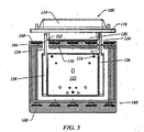
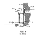
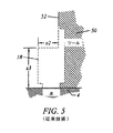
図4及び図5は、FOUP(例えば、Asyst Tchnologies, Inc.製IsoPort(登録商標))を取り扱うための従来の載せポート部10を示している。載せポート部10は、最低でもSEMI規格E15.1、E47.1、E57、E62、E63、E64、S2−93A、S8−95及び1300Lを順守する。載せポート部10は、とりわけ、ハウジング11と、FOUP前進プレート組立体12と、運動プレート13と、ポート扉14と、開口(図示せず)を有する締結又は取付けプレート16とを有している。取付けプレート16は、処理ツール50の前端部52に、例えばBOLTSインタフェースを介して固着される。取付けプレート16は、単一構造体で構成されていてもよいし、複数部分で構成されていてもよい。ポート扉14は、閉位置(図4に示す)と開位置の間を移動する。用語「閉位置」は、ウェーハ等の物品が取付けプレート16の開口を通過しないようにするポート扉14の任意の位置を意味する。用語「開位置」は、ウェーハ等の物品が取付けプレート16の開口を通過することを可能にするポート扉14の任意の位置を意味し、ポート扉14が開口のいかなる部分も遮断しない位置を含む。
4 and 5 show a conventional
運動プレート13は、FOUP2を受け取り且つ支持するように構成されている。運動プレート13は、とりわけ、運動ピン18と、ラッチ組立体と、FOUP検出センサとを有している。運動ピン18は、FOUPを運動プレート13上に整列させる。ラッチ組立体は、FOUPを運動プレート13に固着させる。FOUP前進プレート組立体12は、運動プレート13を載せ/下ろし位置と、FOUP扉がポート扉14の近くに配置される位置との間を水平方向に移動させる。載せ/下ろし位置において、FOUPは、例えば、OHTシステム又はAGVによって、運動プレート13上に又は運動プレート13上から移送される。運動プレート13をポート扉14に向かって移動させることにより、ポート扉がポート扉と連結したりそれから分離したりすることを可能にし、FOUP内に格納したウェーハへのアクセスを提供する。FOUP前進プレート組立体12及び運動プレート13はいずれも、垂直方向に移動しない。従って、床ベース型輸送システムは、FOUPを運動プレート13から載せたりそれに下ろしたりするための装置(例えば、ロボットアーム)を有しなければならない。
The
図4は、軌道システムの設備用床に沿って移動する、RGV等の従来の床ベース型輸送システムを示している。軌道システム(輪郭30として示す)は、設備の中を移動し、最終的に、載せポート部10のハウジング11に隣接して通る。FOUPを運ぶRGVは、載せポート部10の前で止まり、FOUPを運動プレート13上に置く。次に、FOUPをポート扉14に向って前進させ、最終的には、ポート扉14がFOUP扉を取外す。
FIG. 4 shows a conventional floor-based transport system such as RGV that moves along the facility floor of the track system. The track system (shown as contour 30) moves through the equipment and eventually passes adjacent to the housing 11 of the
図5は、従来の載せポート部10が、ツール50(輪郭18として示す)の前の領域を占めていることを示す。輪郭18は、殆どハウジング11から成り、全体的には、図5に図示していない幅を有する矩形容積を占め、この矩形容積は、処理ツール50の前端52から外方に延びる深さX2と、垂直方向高さX3とを有している。載せポート部10と組み合わされたAGVは、ツール50から外方に(例えば、X1+X2)延び、設備用床4の大きな設置面積を占める。
FIG. 5 shows that the conventional
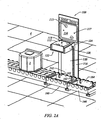
図1〜図3は、本発明の一実施形態を示し、この実施形態は、床取付け型コンベヤ160と、載せポート部100とを有し、載せポート部100は、垂直方向に移動可能なFOUP前進プレート組立体122を有している。コンベヤ160及び載せポート部100は、従来の載せポート部10自体がツールから外方に延びている距離(例えば、X2)よりもツール101から外方に延びていない。コンベヤ160が、ツール101からFOUP前進プレート組立体122よりも外方に延びることも、本発明の範囲内にある。用語「コンベヤ」は、材料、包装体又は品物を1つの箇所から他の箇所に輸送する機械装置等の、搬送装置を意味する。単なる例示として、物品は、ローラ、空気軌道、鉄道、ベルト、又は当業技術の範囲内で知られている任意その他の手段によって、コンベヤ160に沿って移動される。
1 to 3 show an embodiment of the present invention, which has a floor-mounted
載せポート部100は、とりわけ、運動プレート112と、ポート扉114と、取付けプレート116と、FOUP前進プレート組立体122とを有している。取付けプレート116は、好ましくは、BOLTSインタフェース、又は、提案されているSEMIのBOLTS−Lightインタフェース(本出願において後で説明する)のいずれかを介してツール101に固着され、また、開口を有している。運動プレート112は、好ましくは、3つの運動ピン118と、SEMI規格E15.1に従った能動容器押下げ機構とを有している。ポート扉114は、開位置と閉位置の間を移動する。単なる例示として、ポート扉114は、前面開放インタフェース機械規格(FIMS: Front Opening Interface Mechanical Standard)扉組立体を含む。この実施形態では、FIMS扉114は、1対の真空カップ115と、1対のラッチキー117とを有している。ラッチキー117は、FOUP扉を開閉する。真空カップ115は、2つの扉が互いに連結されるとき、FOUP扉とポート扉の間の領域を排気する。FIMS扉114は、図1に示す実施例に限定されず、他の特徴を有していてもよい。更に、載せポート部100がポート扉114を有していないことは、本発明の範囲内である。
The
FOUP前進プレート組立体122は、運動プレート112を水平方向に移動させるための駆動部126を有している。運動プレート112は、FOUPの底面を支持し、FOUPを取付けプレート116の開口に対して整列させる。駆動部126は、運動プレート112を第1の位置(図2A〜2D参照)と第2の位置(図2E〜2F参照)との間で移動させる。第1の位置では、OHTシステムは、FOUP2を運動プレート112から載せたりそれから下ろしたりする。第1の位置はまた、FOUP2をコンベヤ又は他の輸送装置から配置したり除去したりするための載せ/下ろし位置に、運動プレート112を配置する。z方向駆動部120がFOUP前進プレート122をコンベヤ160まで下降させる前に、FOUP前進プレート組立体122が運動プレート112を第1の位置まで移動させてもよいし、FOUP前進プレート組立体122が垂直方向に移動している間に、運動プレート112を水平方向に移動させてもよい。
The FOUP
運動プレート112が水平方向に全く移動しないことも、本発明の範囲内にある。例えば、FOUP前進プレート組立体122を垂直方向に上昇させた後、ポート扉114がFOUP扉に向かって水平方向に移動し、FOUP扉を分離してそれを取外してもよい。また、容器が機械的に開放可能な扉を持たない場合、ポート扉が全く必要でないことがある。この場合、容器をコンベヤから、ツールが物品にアクセス可能な高さまで上昇させるのがよい。
It is also within the scope of the present invention that the
図2Aは、一実施形態において、1対の支持体124が、FOUP前進プレート組立体122をz方向駆動機構120に連結することを示している。本発明は、図2Aに示す支持体124に限定されない。実際、FOUP前進プレート組立体122をz方向駆動機構120に連結する任意の支持機構が十分なものである。単なる例示として、単一の支持体がFOUP前進プレート組立体122をz方向駆動機構120に連結するのがよい。支持体124は、当業技術の範囲内で既知の任意の構造体によって、FOUP前進プレート組立体122及びz方向駆動機構120に連結されるのがよい。z方向駆動機構120は、当業技術で既知の任意の駆動組立体を有するのがよい。
FIG. 2A illustrates that in one embodiment, a pair of
載せポート部100は、FOUP前進プレート組立体122の下に位置するハウジングを含んでおらず、このことは、従来の載せポート部と同様である(例えば、載せポート部10のハウジング11)。従って、FOUP前進プレート組立体122と設備用床4との間の領域には、障害となる構成要素がない。言い換えると、FOUP前進プレート組立体122は、実質的に垂直方向に且つ取付けプレート116に対して平行に移動することができる。本発明を説明する目的のために、FOUP前進プレート組立体122は、最大高さ(図2A参照)と最小高さ(図2B参照)の間を垂直方向に移動する。FOUP前進プレート組立体122は、これら2つの高さの間の任意の位置に移動することができる。FOUP前進プレート組立体122が、その他の高さ(例えば、取付けプレート116の開口の上)の間を移動することも本発明の範囲内である。
The
FOUP2をコンベヤ160から取り上げるために、FOUP前進プレート組立体122は、最小高さ位置に配置される。そうするために、z方向駆動機構120は、FOUP前進プレート組立体122を図2Bに示す位置まで下降させる。FOUP前進プレート組立体122が最小高さ位置にある間、FOUP前進プレート組立体122は、好ましくは、コンベヤ160の第1のレール164と第2のレール166の間にある。FOUP前進プレート組立体122は、コンベヤ160に沿って移動するFOUP2が運動プレート112の上を障害なしに通ることができるように十分下降させられなければならない。この実施形態では、運動プレート112は、第1のレール162と第2のレール164との間に位置する前位置、即ち、ポート扉から離れた位置まで移動させられる。
In order to pick up the
図2Cは、運動プレート112の上方で且つコンベヤ160上で完全に停止しているFOUP2を示している。FOUP2は、好ましくは、運動ピン118とFOUP2の底面のピンレセプタクルとが整列するとき、運動プレート112の上で完全に静止する。FOUP2及び運動プレート112が整列している間、z方向駆動機構120は、FOUP前進プレート組立体122を上昇させる。z方向駆動機構120がFOUP前進プレート組立体122を最大高さ位置に向かって上昇し続けると、ついには、運動プレート112がFOUP2の底面と接触し、FOUP2をコンベヤ160から持上げる(図2D参照)。FOUP2内のウェーハにアクセスするために、FOUP2と運動プレート112との間の更なる調節は必要でない。
FIG. 2C shows the
図2A〜図2Cに示すコンベヤ160は、FOUP2を、それが載せポート部10に達するときにFOUP扉が載せポート部に面するように輸送する。FOUP2を他の配向のコンベヤに沿って輸送することも、本発明の範囲及び精神内にある。単なる例示として、FOUP2が移動する方向にFOUP扉が面した状態で、FOUP2がコンベヤに沿って移動してもよい。この場合、FOUP前進プレート組立体122は、それがFOUP2をコンベヤ160から取り上げた後、FOUP扉が載せポート部に面するようにFOUP2を90度回転させる。
The
この時点で、FOUP前進プレート組立体122は、運動プレート112をポート扉114に向かって移動させる。FOUP扉が、それを分離して取外すのに十分FOUP扉に十分近くになるまで、FOUPを前方に移動させる。単なる例示として、FOUP扉のロックを解除してFOUP扉を取外し且つFOUP及びポート扉をツール内で輸送することができるポート扉が、Asyst Technologies,Inc.に譲渡された「アラインメントピンのないFIMSインタフェース」と題する米国特許第6,419,438号(特許文献1)に説明され、この内容を本明細書に援用する。図2Fは、運動プレート112上に位置するFOUP2内のウェーハが処理されている間、製造設備内の別のFOUPが別の処理ツールまでコンベヤ160に沿って障害なしに移動することを示している。
At this point, the FOUP
FOUP2は、コンベヤ160の第1のレール164及び第2のレール166に沿って移動する。図3は、FOUP前進プレート組立体122が最小高さ位置にある間、レールが、好ましくは、FOUP前進プレート組立体122をレール間に収容するように離間されていることを示している。図1〜図3の実施形態では、載せポート部100の前に位置するコンベヤ160の各セクションは、2つのスロット162を第1のレール164に含んでいる。各スロット162により、FOUP前進プレート組立体122が最小高さ位置まで下降したとき(図2B参照)、支持体124が第1のレール164を貫くことを可能にする。スロット162は、コンベヤ160に沿って移動するFOUP2が、運動プレートの上を障害なしに通り過ぎることができる位置まで、z方向駆動機構120が運動プレート112を下降させることを可能にする。支持体124を収容する第1のレール164に対する任意の修正は、本発明の精神及び範囲内である。同様に、載せポート部100が1つの支持体124を含むに過ぎない場合、第1のレール164は、スロット162を1つしか必要としない。
The
図1及び図2は、床取付け型コンベヤ160のいくつかの特徴を示している。コンベヤを製造設備内の任意の高さに設置することは、本発明の範囲内にある。単なる例示として、コンベヤ160は、設備用床4の下に位置していてもよいし(例えば、図11)、設備用床4と同一平面(例えば、図10)に位置していてもよいし、載せポート部の上(図示せず)に位置していてもよい。
1 and 2 illustrate several features of the floor mounted
載せポート部に対するコンベヤシステムの高さに関わらず、FOUP2が載せポート部100に達したときにFOUP扉6がポート扉に面するように、各FOUP2がコンベヤ160に沿って移動することが好ましい。しかしながら、FOUPは、他の配向のコンベヤに沿って移動し、最終的に、ポート扉に面するように回転させられてもよい。いずれにしても、各FOUP2がコンベヤと載せポート部の間で取扱われる回数は、大いに減少する。例えば、FOUPがコンベヤからFOUP前進プレート組立体によって持上げられた後、ウェーハにアクセスする前に、FOUPを再び整列させる必要はない。FOUPは、コンベヤから持上げられており、例えばRGVシステムに必要なロボットアームによって取扱われる必要はない。載せポート部100は、追加の取扱い工程をなくし、それにより、コンベヤ又は他の輸送装置から載せポート部までのFOUPのより速い移送を実現し、FOUP2の取扱いを最小にする。
Regardless of the height of the conveyor system relative to the loading port portion, each
従来の載せポート部は、床ベース型FOUP輸送システムがFOUPをFOUP前進プレート組立体122の下に直接輸送することを許さない。ハウジング11がFOUP前進プレート組立体と設備用床4との間の空間全体を占めている。図8〜図11は、本発明による載せポート部100と共に使用するためのFOUP輸送システムの実施例を示す。しかしながら、他のFOUP輸送システムも、本発明の精神内及び範囲内にある。
The conventional loading port section does not allow the floor-based FOUP transport system to transport the FOUP directly under the FOUP
図8は、設備用床4の上に上昇させたコンベヤ160を示す。このコンベヤ160は、各載せポート部におけるSEMI指定PGVドッキング領域「トウキック」のための空間を有している。このコンベヤ160は、FOUP2をコンベヤ160(位置B)とFOUP前進プレート組立体122の最高位置(位置A)との間で移動させるのに必要なz方向ストロークを最小にする。設備用床4が適所に留まり、且つ、床タイルとの整列が必要ないので、コンベヤの設置は簡単である。
FIG. 8 shows the
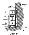
図9は、薄型コンベヤ160を示す。この薄型コンベヤ160は、ツール作業者のためのステップオーバー領域を容易に有する。FOUPは、上述したように、位置Aと位置Bの間を移動させられる。ステップオーバー領域により、例えば、フェンス又はレール150が切欠き部分(図1を参照)を有する場合、作業者がコンベヤ160の上を徒歩で通行することを可能にする。薄型コンベヤはまた、作業者が、例えば載せポート部100の保守のために、載せポート部100をコンベヤの上に持上げることを容易にする。
FIG. 9 shows a
図10は、設備用床4の中に埋込まれたコンベヤ160を示す。この実施形態では、FOUP2の底面3は、実質的に床レベルでコンベヤ160に沿って移動する。コンベヤ160は、載せポート部100の前へのアクセスを妨げない。図8及び図9に示すコンベヤと比較して、コンベヤ160(位置B)と最高位置(位置A)との間のz方向ストロークの必要が増大し、床4は、コンベヤ160のための部屋を許すように修正されなければならない。しかしながら、この埋込み式コンベヤ160は、いくつかの利点を有する。コンベヤ160のホイールは、例えば、処理ツール101の間に位置する領域内の設備用床4内に低く引っ込められ、それにより、徒歩通行でコンベヤ160上を容易に歩くことを可能にし、また、装置をコンベヤ160の上方で転がすことを可能にする。変形例として、一時的なプレートを、ホイールのためのクリアランスを設けてコンベヤ160の上に配置してもよく、それにより、徒歩通行及び装置の容易な転がしを可能にする。
FIG. 10 shows the
図11は、設備用床4の下に位置するコンベヤ160を示す。この実施形態は、コンベヤ160によって完全に邪魔されることなしに、徒歩通行及び装置の転がりを可能にする。この実施形態におけるコンベヤ160(位置B)と最高位置(位置A)との間のz方向ストローク要件は、図8〜図10に示すコンベヤよりも遥かに大きい。
FIG. 11 shows the
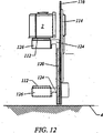
図13〜図16は、設備用床(図11参照)の下に位置するコンベヤと共に用いるために位置Aと位置Bの間でFOUP前進プレート組立体222を移動させるための2段「伸縮式」z方向機構220の実施形態を示す。引込んだ機構240は、それが引込み位置にあるときに設備用床4の上に位置することが好ましい。この特徴により、載せポート部200の容易な取外しを可能にする。伸縮式z方向機構220はまた、第2のz方向ガイド242が作動されない限り、床取付け型コンベヤ160を有する製造設備に用いられる。載せポート部100と同様、FOUP前進プレート組立体222は、位置Aまで上昇させられ、それにより、FOUPがコンベヤ160に沿って移動し且つFOUP前進プレート組立体222の下を通ることを可能にする。
FIGS. 13-16 show a two-stage “retractable” for moving the FOUP
図13〜図15は、2つの処理ツール101を示す。各処理ツール101は、2つの載せポート部200を含む。上述した載せポート部と同様、各載せポート部は、I/Oポート215を有する取付けプレート216と、ポート扉214と、運動プレート212と、z方向駆動機構220とを有している。z方向駆動機構220は、FOUP前進プレート組立体222をI/Oポート215とコンベヤ160の間で垂直方向に移動させる。z方向駆動機構220は、2段機構を有し、この2段機構は、第1段駆動機構(FSD)240と、第2段駆動機構(SSD)242とを有している。第1段駆動機構(FSD)240は、FOUP前進プレート組立体222をI/Oポート215と設備用床4の間で垂直方向に移動させる。第2段駆動機構(SSD)242は、FSD240を設備用床4とI/Oポート215の間で垂直方向に移動させる駆動部組立体を有している。一実施形態では、SSD242は、FSD240の背面チャンネル250内に着座し、FSD240のためのガイドを構成する。しかしながら、本発明は、この構造に限定されない。FSD240がその完全上昇位置に配置されるとき、FSD240が取付けプレート216よりも下に延びないことが好ましい。この特徴により、載せポート部200が処理ツール201から容易に取外されることを可能にする。
13 to 15 show two
図16及び図17は、高さを低くした取付けプレート216を有する載せポート部200を示す。高さを低くした取付けプレート216は、上述した取付けプレート116と同様、処理ツール101にBOLTSインタフェースを介して固着されている。しかしながら、図17に示すように、取付けプレート216が処理ツールに固着されているとき、取付けプレート216は、設備用床4まで下方に延びていない。その代わりに、取付けプレート216の底面と設備用床4との間に、隙間が残る。この隙間は、載せポート部200全体を処理ツールから取外す必要なしに処理ツールを保守するアクセスポートを構成する。アクセスポートは、通常、作動中に粒子がアクセスポートを通って処理ツールに入らないように、処理ツールに固着されたブランクプレート(図示せず)によってカバーされている。処理ツールへのアクセスが必要な時はいつでも、ブランクプレートを取外すことができる。高さを低くした取付けプレート216はまた、作業者が載せポート部を処理ツールから取外して、載せポート部を床ベース型輸送システムよりも上に持上げることを可能にする。例えば、ブランクプレートを処理ツールに固着させたまま、取付けプレート216を処理ツールから取外してもよく、それにより、載せポート部を取扱うのに載せポート部をより軽くする。
16 and 17 show a
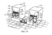
図18は、容器がトンネル190内において設備の中を輸送されてもよいことを示している。トンネル190は、アクセスポートを有し、FOUPを得るために、FOUP前進プレート組立体122をアクセスポートを通してトンネル190内に下降させることを可能にすることが好ましい。トンネル190が、FOUP前進プレート組立体122の垂直方向移動経路を包囲する垂直方向セクションを含むことも、本発明の範囲内にある。これらの垂直方向セクションは、開放した容器又はカセットを設備の中で輸送する輸送システムに対して有用である。この実施形態では、容器の移動経路全体は、設備の残部から隔離される。開放した容器を輸送する垂直方向トンネルセクションも、物品マッピング機能を有するのがよい。例えば、垂直方向トンネルセクションは、容器が垂直方向に移動可能な支持プレートによって開口に向かって持上げられるとき、容器内の各ウェーハの位置を決定する光学走査組立体を含むのがよい。
FIG. 18 shows that the container may be transported through the facility within the
図18、図19、図23、図24は、I/Oポート315とコンベヤ160(又は他のFOUP輸送装置)との間を垂直方向に移動するFOUP前進プレート組立体を有する載せポート部の更に別の実施形態を示す。この実施形態では、載せポート部300は、FOUP前進プレート組立体322と、運動プレート312と、ポート扉314と、I/Oポート315を有する取付けプレート316とを含む。この実施形態では、取付けプレート316は、処理ツール101にBOLTS−Lightインタフェースを介して固着されている。
18 , 19 , 23, and 24 further illustrate a loading port portion having a FOUP advance plate assembly that moves vertically between I /
z方向駆動機構320は、FOUP前進プレート組立体322をI/Oポート315とコンベヤ160との間で垂直方向に移動させる。z方向駆動機構320は、第1のz方向ガイド302と、第2のz方向ガイド304とを有している。各z方向ガイドは、I/Oポート315の側において、取付けプレート316に固着されている。各z方向ガイドはまた、取付けプレート316と一体に形成されるのがよい。z方向駆動機構320はまた、1対のz方向レールを含む。この実施形態では、第1のz方向レール306は、第1のz方向ガイド302内を移動し、第2のz方向レール308は、第2のz方向ガイド304内を移動する。z方向レール306、308の少なくとも一方は、FOUP前進プレート組立体322に固着されている。従って、z方向レール306、308を移動させることは、FOUP前進プレート組立体322をI/Oポート315とコンベヤ160との間で垂直方向に移動させることである。コンベヤ160は、好ましくは、最下位置に配置されたFOUP前進プレート組立体322を収容するように修正される(例えば、スロット162)。図18及び図19に示す載せポート部300は、FOUP前進プレート組立体322を床取付け型コンベヤまで下降させる。z方向機構301はまた、メンテナンスを容易にするために、z方向ガイド302、304及び駆動機構(図示せず)を設備用床4の上方に保ちながら、床下コンベヤ適用例のためのより長い移動ストロークに適合するように用いられる。
The z-
図8〜図11は、コンベヤと設備の残部との間の物理的構造体を構成する障壁150の一実施形態を示す。障壁150は、コンベヤ160に沿ったFOUPの移動との干渉を防止する。別の実施形態では、コンベヤ160は、トンネル190によって設備から隔離される(図18参照)。トンネル190は、載せポート部に隣接して配置されているところにおいて、その上面に開口を含むことが好ましい。トンネル190の開口により、コンベヤ160上を移動するFOUPへのFOUP前進プレート組立体のアクセスを可能にする。
8-11 illustrate one embodiment of a
これらのコンベヤは、FOUPを半導体製造設備の中で輸送する。好ましい実施形態では、各FOUPは、最上位置に位置する各FOUP前進プレート組立体122の下方においてコンベヤに沿って移動する。輸送装置を各載せポート部の基準面よりも下に配置することは、コンベヤ160によって発生した粒子の影響を最小にする。
These conveyors transport FOUPs within a semiconductor manufacturing facility. In the preferred embodiment, each FOUP moves along the conveyor below each topmost FOUP
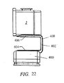
図20から図22は、2つのFOUPを支持すると同時に軌道420に沿って輸送するためのシャトル400の一実施形態を示す。シャトル400が2つよりも多い又は少ないFOUPを保持することは、本発明の範囲内にある。この実施形態では、シャトル400は、2組の支持体402を含み、支持体の各組は、単一のFOUP2を支持する。各支持体402は、好ましくは、垂直部材408によって上支持体406から分離した下支持体404を含む。上支持体及び下支持体は、最下位置に配置されたFOUP前進プレート組立体122と共に載せポート部を通るシャトル400が邪妨害されることなしに載せポート部を通るように分離される。上支持体406は、FOUPの底面を最小の接触状態で支持するように構成される。
Figures 20 22 illustrate an embodiment of a
シャトル400はまた、垂直方向に移動するFOUP前進プレート組立体122を収容する。例えば、上支持体406は、好ましくは、FOUP前進プレート組立体122の幅よりも大きい距離だけ分離される。シャトル400が載せポート部の前で静止するとき、最下位置に配置されたFOUP前進プレート組立体122は、上支持体406と下支持体404の間に位置し、垂直方向支持体408と干渉しない。
The
FOUPをシャトル400から載せポート部100の運動プレート112に移送するために、最初、FOUP前進プレート組立体122を最下位置まで下降させる。次に、シャトル400を、載せポート部100の前の軌道420上で静止させる。この時点で、FOPU2の底面の運動ピン用の溝は、好ましくは、運動プレート112上の運動ピン118と整列する。次に、FOUP前進プレート組立体122を、最上位置まで上昇させる。最終的に、FOUP2を運動プレート112に係合させ、シャトル402の上支持体406から持上げる。好ましい実施形態では、FOUPを取付けプレート16に向かって移動させて、FOUP扉6を取外すために、FOUP2と運動プレート112との間の更なる調節は必要ない。
In order to transfer the FOUP from the
レール420は、コンベヤ又は従来の軌道等の当該技術の範囲内で既知の任意の機構を有するのがよい。レール420はまた、多くの高さで製造設備内に取付けられてもよい。例えば、レール420は、設備用床4に対して同一平面に取付けられてもよいし、それよりも下に取付けられてもよいし、それよりも上に取付けられてもよい。シャトル400を上昇させないならば、シャトル400は、好ましくは、レール420の上の作業者の徒歩通行を可能にする低輪郭を有する。
The
シャトル400は、任意の種類のレールに沿って移動するのがよい。単なる例示として、レール420は、1次駆動レール422と、2次支持レール424とを有する。図20から図22に示すシャトル400は、2つの300mmFOUP2A、2Bを同時に輸送することができる。シャトルが2つ又はそれよりも多くのFOUPを運ぶことは、本発明の精神内及び範囲内にある。FOUP2A及び2Bを1つのシャトル400で同時に輸送することにより、より柔軟性のある配送シーケンスを可能にし、バッファ機能の利点をもたらす。例えば、2つのポッドシャトル400は、「高速スワップ(fast swaps)」を行う機能を有する。言い換えれば、シャトル400は、第1のFOUP2Aを載せポート部100Aから空の支持体402の上に回収し、次に、第2のFOUP2Bをシャトル400から同じ載せポート部100Aに載せる。これにより、最終FOUPを未処理ウェーハを有する新しいFOUPと交換するのに必要な時間(例えば、FOOUP内のウェーハが処理段階を終える)が非常に短いと考えられるので、各処理ツール101に必要な載せポート部100の数を低減させる。
The
従来の処理ツールは、しばしば、別の載せポート部が処理中のFOUPを保持する間、載せポート部からそれを除去するように、仕上げ済みFOUPが着座してAMHS(例えば、OHTシステム)がFOUPを載せポート部から取外すことを待つことができるように且つ新しいFOUPが第3の載せポート部にAMHSから載せられることができるように、多数の載せポート箇所を有する。例えば、図16は、2つの載せポート部、すなわち、第1の載せポート部100Aと第2の載せポート部100Bとを有する処理ツール101を示す。2つの載せポート部を有することにより、AMHSによるゲート動作なしに連続ツール作動を可能にする。高速スワップシャトル400であれば、連続ツール作動を達成するのに、第3の載せポート部は不必要である。
Conventional processing tools often have the finished FOUP seated and the AMHS (eg, OHT system) FOUP so that it removes it from the loading port while another loading port holds the FOUP being processed. It has a number of loading port locations so that it can wait to be removed from the loading port portion and so that a new FOUP can be loaded from the AMHS to the third loading port portion. For example, FIG. 16 shows a
3つ又は4つのFOUPを収容することができるシャトル400は、各ツールにおいて高速スワップで順次2つ又は3つの処理ツールを保守することができる。シャトルはまた、起点、恐らくはストッカーから3つ又は4つのFOUPを取ることができ、FOUPを連続して1つのトリップ内の3つ又は4つのツールに配送することができる。例えば、いくつかのFOUPは、ベイを上がって北向きの行程中(例えば、処理ツール101Aから処理ツール101Bに移動するシャトル400)、様々なツールから載せられたり下ろされたりする。ベイは、限定するわけではないが、一列に配置された多数のツールとして定められる。次に、シャトル400は、逆方向に移動し(処理ツール101Bから処理ツール101Aに移動するシャトル400)、いくつかのFOUPは、南向きの行程中、様々なツールから載せられたり下ろされたりする。
A
レールシステムは、シャトル400を設備用床4上で、設備用床4の上方で、設備用床4の下方で、ベイの間で及びベイ内で様々な経路に沿って移動させるために、分岐したり、湾曲したり、斜めに上ったり、斜めに下がったりする。全てのシャトル400は、基準に対するポッド位置の観点で、同一に作られる。これにより、ロボットアームを組み込む最新のAGVが必要とするツールの「ティーチング(teaching)」をなくす。このことは、シャトルを取外したり置換したりする有用性及び時間を改善する。
The rail system branches to move the
シャトル400は、例えば、チューブ190に包囲された時又はフェンス150の背後にあるときだけ、高速で移動してもよい。囲いがない領域では、例えば、徒歩通行横断を可能にするために、シャトル400は、より低速のモードで移動し、衝突を回避するために、前方監視センサを有し又は光のカーテンの背後を移動するのがよい。徒歩通行との交差点は、物理的ゲートを有していてもよいし、徒歩通行がレールを通り過ぎてもよいかどうかを指示する交通信号システムを有していてもよい。
The
無レールシャトル、すなわち、AGVは、床、天井、壁上、又は載せポート部及び同様の構造体上に設置した基準に対して床上の可視線に従い、操縦される(例えば、推測式)。無レールシャトルは、徒歩通行及び機器ローリングのために床を邪魔されないままに残すこと、レールの費用を排除すること、隣接ツール間の直線的な動きに対してシャトル運動を制限しないことのようないくつかの恩典をもたらす。例えば、無レールシャトルは、通路の反対側に位置する連続処理段階を実施するツール間でFOUPを輸送するためにベイ通路を横切ることができ、シャトルは、必要に応じて互いを追い越すことができると考えられる。更に、個々のツールは、保守のためのラインから外すことができ、無レール車は、この保守中に載せポート部領域の周囲で簡単に方向を変えることができる。最新式車は、工場全体を操縦し、エレベータに入り、ツール作業者によって占められた通路も同様に下りることができる。 A railless shuttle, or AGV, is maneuvered (eg, inferred) according to the visible line on the floor relative to a reference installed on the floor, ceiling, wall, or on the loading port and similar structures. Rail-free shuttles such as leaving the floor undisturbed for walking and equipment rolling, eliminating rail costs, and not limiting the shuttle movement to linear movement between adjacent tools. Bring some benefits. For example, a rail-free shuttle can traverse bay passages to transport FOUPs between tools performing continuous processing steps located on opposite sides of the passage, and shuttles can overtake each other as needed. it is conceivable that. Furthermore, individual tools can be removed from the maintenance line, and railless vehicles can be easily turned around the port area during this maintenance. A state-of-the-art car can navigate the entire factory, enter the elevator, and go down the aisle occupied by tool workers as well.
図25〜図27は、載せポート部が、FOUPを水平に移動させるための容器前進組立体又はポート扉のいずれかを有する必要なく、2つの高さの間でFOUPを水平にただ移動させる必要がある可能性があることを示している。例えば、図25は、載せポート部500が、とりわけ、開口517及び垂直方向に移動可能な支持構造体522を有する取付けプレート516を含むことを示している。上述の実施形態と同様、載せポート部500はまた、支持構造体522をコンベヤ560と開口517の間で垂直方向に移動させるための機構を含む。図25の実施形態は、FOUPの底面に接触するための2つの支持体を有する支持構造体522を示している。
FIGS. 25-27 show that the loading port portion need only move the FOUP horizontally between two heights without having to have either a container advancement assembly or a port door for moving the FOUP horizontally. Indicates that there may be. For example, FIG. 25 shows that the
図25に示すコンベヤ560は、支持構造体522を収容するために各載せポート部500のところで3つのセクションに分割される。単なる例示として、コンベヤ560は、中央セクション562と、左セクション564と、右セクション568とを有している。この実施形態の各コンベヤセクションは、ベルト568と、1対のローラ570とを有している。一実施形態では、図25に示すように、コンベヤ560の中央セクション562の一部であるローラ570は、取付けプレート516に回転可能に取付けられている。
The
コンベヤ560の各セクションは、互いに分離され、コンベヤの各セクション間に隙間を形成する。この隙間により、支持構造体522がコンベヤ560の下を移動すること、及び、FOUPがコンベヤ560の中央セクション562に到着するのを待つことを可能にする。FOUPが中央セクション562に到着して静止した後、支持構造体522は、FOUPの底面に係合するように垂直方向に上昇し、FOUPをコンベヤ560から持上げるのがよい。
The sections of the
図26は、載せポート部600及びコンベヤ660を有する輸送及び配送システムを示す。載せポート部600は、とりわけ、取付けプレート616と、支持構造体622と、支持構造体622を垂直方向に移動させるための機構620とを有している。この実施形態では、支持構造体622は、構造体を含み、この構造体は、第1の支持体624と、第2の支持体626と、第3の支持体628とを有している。各支持体は、その遠位端のところに運動ピン618を有している。この構造体は、載せポート部100の運動プレート112に置き換わる。単なる例示として、コンベヤ660は、レール662と、多数の片持ちローラ664とを有している。図26Bに示すように、支持構造体622の各支持体624、626、628は、支持構造体622をローラ664よりも下に下降させることができるように、1対の隣接したローラ664の間を通ることができる。FOUPは、好ましくは、支持構造体622上の運動ピン618と整列したFOUPの底面の運動溝と共にローラ664上で静止する。次に、支持構造体622を垂直方向に上昇させ、FOUPの底面に係合させ、FOUPを所定の高さまでコンベヤ660から持上げる。
FIG. 26 shows a transportation and delivery system having a
図27は、別の輸送及び配送システムを示し、この輸送及び配送システムは、載せポート部700と、コンベヤ760とを有している。載せポート部700は、とりわけ、開口716及びスロット724を有する取付けプレート716と、支持構造体722とを有している。この実施形態では、支持構造体722は、好ましくは、開口717とコンベヤ760の間で垂直方向にのみ移動する。しかしながら、支持構造体722が水平方向にも移動することは、本発明の範囲内にある。支持構造体722は、限定するわけではないが、FOUPを支持するための運動プレート又は任意その他の容器支持機構を含む容器を支持する任意の構造体を含むことができる。コンベヤ760は、各ローラ764の両端に位置する回転可能ホイール766を有する片持ちローラ764を有するレール762を含む。この実施形態では、ローラ764は、好ましくは、容器との接触を最小にするためにホイール766だけで容器とは接触しない。
FIG. 27 shows another transportation and delivery system, which has a
載せポート部700のすぐ前に位置する容器を支持するために、2つのホイール766が、載せポート部700の取付けプレート716に回転可能に取付けられる。これら2つのホイールは、受動ホイールであってもよいし、駆動ホイールであってもよい。載せポート部700の前のセクションのためのコンベヤ760上のローラ764をなくすことにより、支持構造体722をホイール766の下に下降させることを可能にする。この時点で、容器が載せポート部700の前で静止するとき、次に、支持構造体722を上昇させて、容器をコンベヤ760から持上げる。図25〜図27に示す支持構造体及びコンベヤは、交換可能である。
Two
コンベヤと載せポート部の間のFOUP輸送のための上述した機構及び方法は、説明だけの目的のものであり、それによって本発明が限定されないことを認識すべきである。かくして、FOUP輸送のための方法及びシステムの好ましい実施形態を説明したので、システム内の一定の利点が達成されたことが当業者に明らかなはずである。様々な修正例、適用例及び変形例の実施形態は、本発明の範囲内及び精神内で行うことができることも認識すべきである。例えば、コンベヤの用途は、半導体製造設備内で示されているが、上述した本発明の概念の多くは、他の半導体製造用途以外の使用に等しく適用可能であると考えられることは明らかであるべきである。 It should be appreciated that the above-described mechanisms and methods for FOUP transport between the conveyor and the loading port section are for illustrative purposes only, and the present invention is not limited thereby. Thus, having described preferred embodiments of methods and systems for FOUP shipping, it should be apparent to those skilled in the art that certain advantages within the system have been achieved. It should also be appreciated that various modifications, applications, and variations of embodiments can be made within the scope and spirit of the invention. For example, conveyor applications are shown in semiconductor manufacturing facilities, but it is clear that many of the inventive concepts described above are considered equally applicable for use other than other semiconductor manufacturing applications. Should.
Claims (19)
(あ)ロードポートを備え、前記ロードポートは、
容器に格納された物品を処理ツールに差し出すための開口を有するフレームと、
容器を受取るように構成された支持構造体と、
上記フレームの開口の位置に対応する最大高さと最小高さの間で垂直方向に前記支持構造体を移動させるための駆動機構と、を有しており、
(い)更に、容器輸送平面に沿って前記容器を移動可能に支持するためのコンベヤを備え、
前記容器は、前記支持構造体が前記最小高さに位置するとき、障害なしに、前記支持構造体の上方にある前記コンベヤ上を移動し、
前記容器は、前記最小高さに配置された前記支持構造体の上方にある前記コンベア上を移動する間、前記容器は、前記支持構造体に接触せず、
前記支持構造体は、前記支持構造体が前記最小高さに配置されているとき、前記容器輸送平面よりも下方に配置され、
前記支持構造体は、前記支持構造体が前記最大高さに配置されているとき、前記容器輸送平面よりも上方に配置され、
前記支持構造体は、前記支持構造体の上方の前記コンベア上にある前記容器を前記最小高さから前記最大高さまで上昇することにより、前記容器を受け取り、この受け取られた容器に格納された物品が、前記支持構造体が前記最大高さの位置にあるとき、前記フレームの開口を通過して前記処理ツールに差し出されるように構成されている、ことを特徴とするシステム。A system for presenting a container containing at least one article to a processing tool,
(A) a load port , the load port is
A frame having an opening for delivering an article stored in the container to a processing tool ;
A support structure configured to receive the container;
It has a drive mechanism for the moving the support structure in the vertical direction between the maximum height and minimum height corresponding to the position of the opening of the frame,
(I) further comprising a conveyor for movably supporting the container along the container transport plane;
The container moves on the conveyor above the support structure without obstruction when the support structure is at the minimum height;
It said container, while moving the upper conveyor located above the supporting structure disposed on the minimum height, the container is not in contact with the support structure,
The support structure is disposed below the container transport plane when the support structure is disposed at the minimum height ;
The support structure is disposed above the container transport plane when the support structure is disposed at the maximum height ;
The support structure receives the container by raising the container on the conveyor above the support structure from the minimum height to the maximum height, and an article stored in the received container. Is configured to pass through the opening of the frame and to the processing tool when the support structure is at the maximum height .
前記支持構造体に固定されたアームと、
前記アームを垂直方向に移動させるための駆動組立体と、
を有することを特徴とする、請求項1に記載のシステム。The drive mechanism is
An arm fixed to the support structure;
A drive assembly for moving the arm vertically;
The system according to claim 1, comprising:
前記コンベヤにおける容器の移動方向と平行な第1のレールと、
前記第1のレールから離間し、且つ、前記第1のレールと平行な第2のレールとを有し、
前記第1のレールのうちの前記ロードポートを通過する部分は、前記アームが前記第1のレールの少なくとも一部を障害なしに通過することを可能にする、
ことを特徴とする、請求項6に記載のシステム。The conveyor is
A first rail parallel to the direction of container movement on the conveyor;
A second rail spaced from the first rail and parallel to the first rail;
The portion of the first rail that passes through the load port allows the arm to pass through at least a portion of the first rail without obstruction.
The system according to claim 6, wherein:
上面を有する第1のレールと、
前記第1のレールから離間した第2のレールと、
を有することを特徴とする、請求項1に記載のシステム。The conveyor is
A first rail having an upper surface;
A second rail spaced from the first rail;
The system according to claim 1, comprising:
ロードポートを備え、前記ロードポートは、
容器に格納された物品を処理ツールに差し出すための開口を有するフレームと、
容器を受取るように構成された支持構造体と、
前記支持構造体に連結され、且つ、前記支持構造体を前記フレームに対して垂直方向に移動させるための機構と、を有しており、
前記機構は、前記支持構造体を前記コンベヤの第1のレールと第2のレールとの間の所定の下方位置まで下降させ、前記容器が、前記支持構造体が前記所定の下方位置に配置されるとき、障害なしに、前記支持体構造体の上方にある前記コンベア上を通るように構成され、
前記支持構造体は、前記支持構造体が前記所定の下方位置に配置されるとき、前記容器輸送平面よりも下方に位置し、
前記機構は、前記支持構造体を所定の上方位置まで上昇させ、前記支持構造体が前記上方位置に配置されるときに、前記コンベヤに沿って移動する別の容器が、前記支持構造体の下方を障害なしに通るように構成され、
前記支持構造体は、前記支持構造体の上方の前記コンベア上にある前記容器を前記下方位置から前記上方位置まで上昇することにより、前記容器を受け取り、この受け取られた容器に格納された物品が、前記支持構造体が前記上方位置にあるとき、前記フレームの開口を通過して前記処理ツールに差し出されるように構成されている、ことを特徴とするシステム。 In a semiconductor manufacturing apparatus having a conveyor that movably supports containers for storing at least one article along a first rail and a second rail between processing tools.
A load port , the load port
A frame having an opening for delivering an article stored in the container to a processing tool ;
A support structure configured to receive the container;
Coupled to said support structure, and has a a mechanism for moving vertically said support structure relative to the frame,
The mechanism lowers the support structure to a predetermined lower position between the first rail and the second rail of the conveyor, and the container is disposed at the predetermined lower position. Is configured to pass over the conveyor above the support structure without obstruction ,
The support structure is positioned below the container transport plane when the support structure is disposed at the predetermined lower position;
The mechanism raises the support structure to a predetermined upper position, and when the support structure is placed in the upper position, another container that moves along the conveyor is below the support structure. Is configured to pass without obstacles,
The support structure receives the container by raising the container on the conveyor above the support structure from the lower position to the upper position, and an article stored in the received container is The system is configured to pass through an opening in the frame and be extended to the processing tool when the support structure is in the upper position .
前記支持構造体に固定された遠位端部を有するアームと、
前記アームを前記フレームに対して垂直方向に移動させるための駆動組立体と、
を有することを特徴とする、請求項13に記載のシステム。The mechanism is
An arm having a distal end secured to the support structure;
A drive assembly for moving the arm in a direction perpendicular to the frame;
The system according to claim 13, comprising:
前記コンベヤは、容器輸送平面に沿って前記容器を移動させるように構成され、
ロードポートを備え、前記ロードポートは、
容器に格納された半導体ウェーハを処理ツールに差し出すための開口を有するフレームと、
前記容器を受取るために水平方向に調節可能な支持構造体と、
前記水平方向に調節可能な支持構造体に固定されたアームと、
前記支持構造体を前記フレームに対して垂直方向に移動させるために前記アームに連結された駆動機構と、を有しており、
前記機構は、水平方向に調整可能な支持構造体を、容器輸送平面よりも低い所定の下方位置まで下降させるように構成され、前記コンベヤに沿って移動する容器が、前記支持構造体が前記下方位置にあるとき、前記支持構造体の上方を障害なしに通り、且つ、前記支持構造体に接触することなく障害なしに通ることを可能にし、
前記機構は、前記水平方向に調整可能な支持構造体を、前記容器輸送平面よりも高い所定の上方位置まで上昇させるように構成され、
前記支持構造体は、前記支持構造体の上方の前記コンベア上にある前記容器を前記下方位置から前記上方位置まで上昇することにより、前記容器を受け取り、この受け取られた容器に格納された物品が、前記支持構造体が前記上方位置にあるとき、前記フレームの開口を通過して前記処理ツールに差し出されるように構成されている、ことを特徴とする半導体製造装置。A semiconductor manufacturing apparatus having a conveyor for movably supporting a container for storing at least one semiconductor wafer between processing tools,
The conveyor is configured to move the containers along a container transport plane;
A load port , the load port
A frame having an opening for feeding a semiconductor wafer stored in a container to a processing tool ;
A support structure that is horizontally adjustable to receive the container;
An arm fixed to the horizontally adjustable support structure;
Has a drive mechanism coupled to said arm to move vertically relative to the frame of the support structure,
The mechanism is configured to lower a horizontally adjustable support structure to a predetermined lower position below a container transport plane, and a container moving along the conveyor is configured such that the support structure is below the support structure. when in position, pass over sides of the support structure without failure, and enables to pass without failure without contacting the support structure,
The mechanism is configured to raise the horizontally adjustable support structure to a predetermined upper position higher than the container transport plane;
The support structure receives the container by raising the container on the conveyor above the support structure from the lower position to the upper position, and an article stored in the received container is The semiconductor manufacturing apparatus is configured to pass through the opening of the frame and be inserted into the processing tool when the support structure is in the upper position .
Applications Claiming Priority (2)
| Application Number | Priority Date | Filing Date | Title |
|---|---|---|---|
| US11/064,880 US7410340B2 (en) | 2005-02-24 | 2005-02-24 | Direct tool loading |
| PCT/US2006/006103 WO2006091593A2 (en) | 2005-02-24 | 2006-02-17 | Direct tool loading |
Publications (3)
| Publication Number | Publication Date |
|---|---|
| JP2008532288A JP2008532288A (en) | 2008-08-14 |
| JP2008532288A5 JP2008532288A5 (en) | 2008-11-27 |
| JP4470225B2 true JP4470225B2 (en) | 2010-06-02 |
Family
ID=36407943
Family Applications (1)
| Application Number | Title | Priority Date | Filing Date |
|---|---|---|---|
| JP2007557103A Expired - Fee Related JP4470225B2 (en) | 2005-02-24 | 2006-02-17 | System for sending containers for storing articles to processing tools, semiconductor manufacturing equipment |
Country Status (5)
| Country | Link |
|---|---|
| US (4) | US7410340B2 (en) |
| JP (1) | JP4470225B2 (en) |
| KR (1) | KR100967357B1 (en) |
| CN (1) | CN100590786C (en) |
| WO (1) | WO2006091593A2 (en) |
Families Citing this family (352)
| Publication number | Priority date | Publication date | Assignee | Title |
|---|---|---|---|---|
| FI116719B (en) * | 2004-04-14 | 2006-02-15 | Metso Paper Inc | Procedure for centering rolls |
| WO2006046580A1 (en) * | 2004-10-25 | 2006-05-04 | Tokyo Electron Limited | Carrying system, substrate treating device, and carrying method |
| US7410340B2 (en) * | 2005-02-24 | 2008-08-12 | Asyst Technologies, Inc. | Direct tool loading |
| KR101099247B1 (en) * | 2005-03-08 | 2011-12-27 | 가부시키가이샤 야스카와덴키 | Load port and load port control method |
| US7771151B2 (en) * | 2005-05-16 | 2010-08-10 | Muratec Automation Co., Ltd. | Interface between conveyor and semiconductor process tool load port |
| US20060283688A1 (en) * | 2005-06-10 | 2006-12-21 | Applied Materials, Inc. | Substrate handling system |
| DE102005039453B4 (en) * | 2005-08-18 | 2007-06-28 | Asys Automatic Systems Gmbh & Co. Kg | Machining plant of modular construction for flat substrates |
| KR100788005B1 (en) * | 2006-04-27 | 2007-12-21 | 에스에스알 엠에프지 코포레이션 | Apparatus for opening and closing cover of cassette for thin film disc |
| TW200909318A (en) * | 2006-08-25 | 2009-03-01 | Aquest Systems Corp | Conveyor transfer system |
| US8814488B2 (en) * | 2007-04-02 | 2014-08-26 | Hitachi Kokusai Electric Inc. | Substrate processing apparatus and semiconductor device manufacturing method |
| TWI475627B (en) | 2007-05-17 | 2015-03-01 | Brooks Automation Inc | Substrate carrier, substrate processing apparatus and system, for reducing particle contamination of substrate during processing and method of interfacing a carrier with a processing tool |
| KR102110585B1 (en) * | 2007-05-17 | 2020-05-13 | 브룩스 오토메이션 인코퍼레이티드 | Side opening substrate carrier and load port |
| US20090067957A1 (en) * | 2007-09-06 | 2009-03-12 | Mitsuhiro Ando | Transport system with buffering |
| ATE550138T1 (en) * | 2007-09-14 | 2012-04-15 | Flexlink Components Ab | LIFTING DEVICE FOR A CONVEYOR SYSTEM, CONVEYOR SYSTEM AND METHOD |
| US8303231B2 (en) * | 2007-09-28 | 2012-11-06 | Taiwan Semiconductor Manufacturing Company Ltd. | Apparatus and method for semiconductor wafer transfer |
| JP2009135232A (en) * | 2007-11-29 | 2009-06-18 | Sinfonia Technology Co Ltd | Load port |
| JP5401842B2 (en) * | 2008-06-17 | 2014-01-29 | 村田機械株式会社 | Transport system |
| KR20110009687A (en) * | 2008-06-20 | 2011-01-28 | 무라텍 오토메이션 가부시키가이샤 | Direct loading to and from a conveyor system |
| JP5338335B2 (en) * | 2008-08-13 | 2013-11-13 | 東京エレクトロン株式会社 | Opening / closing device and probe device of transfer container |
| US10378106B2 (en) | 2008-11-14 | 2019-08-13 | Asm Ip Holding B.V. | Method of forming insulation film by modified PEALD |
| JP5381054B2 (en) * | 2008-12-02 | 2014-01-08 | シンフォニアテクノロジー株式会社 | Load port |
| US20100162954A1 (en) * | 2008-12-31 | 2010-07-01 | Lawrence Chung-Lai Lei | Integrated facility and process chamber for substrate processing |
| US8367565B2 (en) * | 2008-12-31 | 2013-02-05 | Archers Inc. | Methods and systems of transferring, docking and processing substrates |
| US8110511B2 (en) * | 2009-01-03 | 2012-02-07 | Archers Inc. | Methods and systems of transferring a substrate to minimize heat loss |
| US7897525B2 (en) * | 2008-12-31 | 2011-03-01 | Archers Inc. | Methods and systems of transferring, docking and processing substrates |
| US20100162955A1 (en) * | 2008-12-31 | 2010-07-01 | Lawrence Chung-Lai Lei | Systems and methods for substrate processing |
| US9394608B2 (en) | 2009-04-06 | 2016-07-19 | Asm America, Inc. | Semiconductor processing reactor and components thereof |
| CN102460675B (en) * | 2009-05-18 | 2015-04-29 | 布鲁克斯自动化公司 | Integrated systems for interfacing with substrate container storage systems |
| EP2433299B1 (en) * | 2009-05-18 | 2022-10-26 | Brooks Automation US, LLC | Substrate container storage system |
| US8882433B2 (en) * | 2009-05-18 | 2014-11-11 | Brooks Automation, Inc. | Integrated systems for interfacing with substrate container storage systems |
| US8802201B2 (en) | 2009-08-14 | 2014-08-12 | Asm America, Inc. | Systems and methods for thin-film deposition of metal oxides using excited nitrogen-oxygen species |
| JP5633738B2 (en) * | 2010-09-27 | 2014-12-03 | 株式会社ダイフク | Goods transport equipment |
| US8956098B2 (en) * | 2011-05-02 | 2015-02-17 | Murata Machinery, Ltd. | Automated warehouse |
| US9312155B2 (en) | 2011-06-06 | 2016-04-12 | Asm Japan K.K. | High-throughput semiconductor-processing apparatus equipped with multiple dual-chamber modules |
| US10364496B2 (en) | 2011-06-27 | 2019-07-30 | Asm Ip Holding B.V. | Dual section module having shared and unshared mass flow controllers |
| US10854498B2 (en) | 2011-07-15 | 2020-12-01 | Asm Ip Holding B.V. | Wafer-supporting device and method for producing same |
| US20130023129A1 (en) | 2011-07-20 | 2013-01-24 | Asm America, Inc. | Pressure transmitter for a semiconductor processing environment |
| CN102945818B (en) * | 2011-08-15 | 2015-06-17 | 上海微电子装备有限公司 | Wafer library device of silicon wafer transmission system |
| US9017481B1 (en) | 2011-10-28 | 2015-04-28 | Asm America, Inc. | Process feed management for semiconductor substrate processing |
| US9558978B2 (en) * | 2012-05-04 | 2017-01-31 | Kla-Tencor Corporation | Material handling with dedicated automated material handling system |
| US8944739B2 (en) * | 2012-06-01 | 2015-02-03 | Taiwan Semiconductor Manufacturing Co., Ltd. | Loadport bridge for semiconductor fabrication tools |
| CN103231898B (en) * | 2012-08-21 | 2015-05-20 | 深圳市捷佳伟创新能源装备股份有限公司 | Lateral embark and disembark device |
| US9659799B2 (en) | 2012-08-28 | 2017-05-23 | Asm Ip Holding B.V. | Systems and methods for dynamic semiconductor process scheduling |
| US10714315B2 (en) | 2012-10-12 | 2020-07-14 | Asm Ip Holdings B.V. | Semiconductor reaction chamber showerhead |
| US9260207B2 (en) * | 2013-01-17 | 2016-02-16 | Sergey N. Razumov | Order picking system and method |
| US20160376700A1 (en) | 2013-02-01 | 2016-12-29 | Asm Ip Holding B.V. | System for treatment of deposition reactor |
| US9589770B2 (en) | 2013-03-08 | 2017-03-07 | Asm Ip Holding B.V. | Method and systems for in-situ formation of intermediate reactive species |
| US9484191B2 (en) | 2013-03-08 | 2016-11-01 | Asm Ip Holding B.V. | Pulsed remote plasma method and system |
| US9008825B2 (en) | 2013-04-01 | 2015-04-14 | Honda Logistics North America, Inc. | Container unloading system with auto-unload capability |
| US9142437B2 (en) * | 2013-04-10 | 2015-09-22 | Globalfoundries Inc. | System for separately handling different size FOUPs |
| US9240412B2 (en) | 2013-09-27 | 2016-01-19 | Asm Ip Holding B.V. | Semiconductor structure and device and methods of forming same using selective epitaxial process |
| US10683571B2 (en) | 2014-02-25 | 2020-06-16 | Asm Ip Holding B.V. | Gas supply manifold and method of supplying gases to chamber using same |
| US10167557B2 (en) | 2014-03-18 | 2019-01-01 | Asm Ip Holding B.V. | Gas distribution system, reactor including the system, and methods of using the same |
| US11015245B2 (en) | 2014-03-19 | 2021-05-25 | Asm Ip Holding B.V. | Gas-phase reactor and system having exhaust plenum and components thereof |
| KR102160106B1 (en) * | 2014-07-03 | 2020-09-25 | 세메스 주식회사 | Apparatus for transferring a wafer |
| WO2016012923A1 (en) | 2014-07-23 | 2016-01-28 | Corob S.P.A. Con Socio Unico | Apparatus for moving receptacles |
| US10858737B2 (en) | 2014-07-28 | 2020-12-08 | Asm Ip Holding B.V. | Showerhead assembly and components thereof |
| US9890456B2 (en) | 2014-08-21 | 2018-02-13 | Asm Ip Holding B.V. | Method and system for in situ formation of gas-phase compounds |
| US9698038B2 (en) * | 2014-08-28 | 2017-07-04 | Infineon Technologies Ag | Adapter tool and wafer handling system |
| US9657845B2 (en) | 2014-10-07 | 2017-05-23 | Asm Ip Holding B.V. | Variable conductance gas distribution apparatus and method |
| US10941490B2 (en) | 2014-10-07 | 2021-03-09 | Asm Ip Holding B.V. | Multiple temperature range susceptor, assembly, reactor and system including the susceptor, and methods of using the same |
| WO2016076722A2 (en) * | 2014-11-14 | 2016-05-19 | Mapper Lithography Ip B.V. | Load lock system and method for transferring substrates in a lithography system |
| KR102263121B1 (en) | 2014-12-22 | 2021-06-09 | 에이에스엠 아이피 홀딩 비.브이. | Semiconductor device and manufacuring method thereof |
| MX359183B (en) * | 2015-02-17 | 2018-09-17 | Solarcity Corp | Method and system for improving solar cell manufacturing yield. |
| US10529542B2 (en) | 2015-03-11 | 2020-01-07 | Asm Ip Holdings B.V. | Cross-flow reactor and method |
| US10276355B2 (en) | 2015-03-12 | 2019-04-30 | Asm Ip Holding B.V. | Multi-zone reactor, system including the reactor, and method of using the same |
| JP6456768B2 (en) * | 2015-05-18 | 2019-01-23 | 株式会社ディスコ | Processing equipment |
| US20160359080A1 (en) | 2015-06-07 | 2016-12-08 | Solarcity Corporation | System, method and apparatus for chemical vapor deposition |
| US10458018B2 (en) | 2015-06-26 | 2019-10-29 | Asm Ip Holding B.V. | Structures including metal carbide material, devices including the structures, and methods of forming same |
| US10600673B2 (en) | 2015-07-07 | 2020-03-24 | Asm Ip Holding B.V. | Magnetic susceptor to baseplate seal |
| US9960072B2 (en) | 2015-09-29 | 2018-05-01 | Asm Ip Holding B.V. | Variable adjustment for precise matching of multiple chamber cavity housings |
| US10211308B2 (en) | 2015-10-21 | 2019-02-19 | Asm Ip Holding B.V. | NbMC layers |
| US10322384B2 (en) | 2015-11-09 | 2019-06-18 | Asm Ip Holding B.V. | Counter flow mixer for process chamber |
| CN105438761B (en) * | 2015-12-18 | 2018-07-31 | 苏州佳世达电通有限公司 | Production line control method and equipment for realizing the control method |
| US11139308B2 (en) | 2015-12-29 | 2021-10-05 | Asm Ip Holding B.V. | Atomic layer deposition of III-V compounds to form V-NAND devices |
| US10468251B2 (en) | 2016-02-19 | 2019-11-05 | Asm Ip Holding B.V. | Method for forming spacers using silicon nitride film for spacer-defined multiple patterning |
| US10529554B2 (en) | 2016-02-19 | 2020-01-07 | Asm Ip Holding B.V. | Method for forming silicon nitride film selectively on sidewalls or flat surfaces of trenches |
| US10501866B2 (en) | 2016-03-09 | 2019-12-10 | Asm Ip Holding B.V. | Gas distribution apparatus for improved film uniformity in an epitaxial system |
| US10343920B2 (en) | 2016-03-18 | 2019-07-09 | Asm Ip Holding B.V. | Aligned carbon nanotubes |
| US9892913B2 (en) | 2016-03-24 | 2018-02-13 | Asm Ip Holding B.V. | Radial and thickness control via biased multi-port injection settings |
| US10190213B2 (en) | 2016-04-21 | 2019-01-29 | Asm Ip Holding B.V. | Deposition of metal borides |
| US10865475B2 (en) | 2016-04-21 | 2020-12-15 | Asm Ip Holding B.V. | Deposition of metal borides and silicides |
| US10367080B2 (en) | 2016-05-02 | 2019-07-30 | Asm Ip Holding B.V. | Method of forming a germanium oxynitride film |
| US10032628B2 (en) | 2016-05-02 | 2018-07-24 | Asm Ip Holding B.V. | Source/drain performance through conformal solid state doping |
| KR102592471B1 (en) | 2016-05-17 | 2023-10-20 | 에이에스엠 아이피 홀딩 비.브이. | Method of forming metal interconnection and method of fabricating semiconductor device using the same |
| US9748434B1 (en) | 2016-05-24 | 2017-08-29 | Tesla, Inc. | Systems, method and apparatus for curing conductive paste |
| US11453943B2 (en) | 2016-05-25 | 2022-09-27 | Asm Ip Holding B.V. | Method for forming carbon-containing silicon/metal oxide or nitride film by ALD using silicon precursor and hydrocarbon precursor |
| US10388509B2 (en) | 2016-06-28 | 2019-08-20 | Asm Ip Holding B.V. | Formation of epitaxial layers via dislocation filtering |
| US9859151B1 (en) | 2016-07-08 | 2018-01-02 | Asm Ip Holding B.V. | Selective film deposition method to form air gaps |
| US10612137B2 (en) | 2016-07-08 | 2020-04-07 | Asm Ip Holdings B.V. | Organic reactants for atomic layer deposition |
| US10714385B2 (en) | 2016-07-19 | 2020-07-14 | Asm Ip Holding B.V. | Selective deposition of tungsten |
| US10381226B2 (en) | 2016-07-27 | 2019-08-13 | Asm Ip Holding B.V. | Method of processing substrate |
| US9887082B1 (en) | 2016-07-28 | 2018-02-06 | Asm Ip Holding B.V. | Method and apparatus for filling a gap |
| US10395919B2 (en) | 2016-07-28 | 2019-08-27 | Asm Ip Holding B.V. | Method and apparatus for filling a gap |
| US9812320B1 (en) | 2016-07-28 | 2017-11-07 | Asm Ip Holding B.V. | Method and apparatus for filling a gap |
| KR102532607B1 (en) | 2016-07-28 | 2023-05-15 | 에이에스엠 아이피 홀딩 비.브이. | Substrate processing apparatus and method of operating the same |
| US9954136B2 (en) | 2016-08-03 | 2018-04-24 | Tesla, Inc. | Cassette optimized for an inline annealing system |
| CN106516688B (en) * | 2016-08-16 | 2019-07-19 | 蔡怀峰 | Limiting device |
| KR102613349B1 (en) | 2016-08-25 | 2023-12-14 | 에이에스엠 아이피 홀딩 비.브이. | Exhaust apparatus and substrate processing apparatus and thin film fabricating method using the same |
| US10410943B2 (en) | 2016-10-13 | 2019-09-10 | Asm Ip Holding B.V. | Method for passivating a surface of a semiconductor and related systems |
| US10643826B2 (en) | 2016-10-26 | 2020-05-05 | Asm Ip Holdings B.V. | Methods for thermally calibrating reaction chambers |
| US11532757B2 (en) | 2016-10-27 | 2022-12-20 | Asm Ip Holding B.V. | Deposition of charge trapping layers |
| US10115856B2 (en) | 2016-10-31 | 2018-10-30 | Tesla, Inc. | System and method for curing conductive paste using induction heating |
| US10714350B2 (en) | 2016-11-01 | 2020-07-14 | ASM IP Holdings, B.V. | Methods for forming a transition metal niobium nitride film on a substrate by atomic layer deposition and related semiconductor device structures |
| US10229833B2 (en) | 2016-11-01 | 2019-03-12 | Asm Ip Holding B.V. | Methods for forming a transition metal nitride film on a substrate by atomic layer deposition and related semiconductor device structures |
| US10643904B2 (en) | 2016-11-01 | 2020-05-05 | Asm Ip Holdings B.V. | Methods for forming a semiconductor device and related semiconductor device structures |
| US10435790B2 (en) | 2016-11-01 | 2019-10-08 | Asm Ip Holding B.V. | Method of subatmospheric plasma-enhanced ALD using capacitively coupled electrodes with narrow gap |
| US10134757B2 (en) | 2016-11-07 | 2018-11-20 | Asm Ip Holding B.V. | Method of processing a substrate and a device manufactured by using the method |
| KR102546317B1 (en) | 2016-11-15 | 2023-06-21 | 에이에스엠 아이피 홀딩 비.브이. | Gas supply unit and substrate processing apparatus including the same |
| US10340135B2 (en) | 2016-11-28 | 2019-07-02 | Asm Ip Holding B.V. | Method of topologically restricted plasma-enhanced cyclic deposition of silicon or metal nitride |
| KR20180068582A (en) | 2016-12-14 | 2018-06-22 | 에이에스엠 아이피 홀딩 비.브이. | Substrate processing apparatus |
| US11447861B2 (en) | 2016-12-15 | 2022-09-20 | Asm Ip Holding B.V. | Sequential infiltration synthesis apparatus and a method of forming a patterned structure |
| US11581186B2 (en) | 2016-12-15 | 2023-02-14 | Asm Ip Holding B.V. | Sequential infiltration synthesis apparatus |
| KR20180070971A (en) | 2016-12-19 | 2018-06-27 | 에이에스엠 아이피 홀딩 비.브이. | Substrate processing apparatus |
| US10269558B2 (en) | 2016-12-22 | 2019-04-23 | Asm Ip Holding B.V. | Method of forming a structure on a substrate |
| US10867788B2 (en) | 2016-12-28 | 2020-12-15 | Asm Ip Holding B.V. | Method of forming a structure on a substrate |
| US11390950B2 (en) | 2017-01-10 | 2022-07-19 | Asm Ip Holding B.V. | Reactor system and method to reduce residue buildup during a film deposition process |
| US10655221B2 (en) | 2017-02-09 | 2020-05-19 | Asm Ip Holding B.V. | Method for depositing oxide film by thermal ALD and PEALD |
| US10468261B2 (en) | 2017-02-15 | 2019-11-05 | Asm Ip Holding B.V. | Methods for forming a metallic film on a substrate by cyclical deposition and related semiconductor device structures |
| US10529563B2 (en) | 2017-03-29 | 2020-01-07 | Asm Ip Holdings B.V. | Method for forming doped metal oxide films on a substrate by cyclical deposition and related semiconductor device structures |
| US10283353B2 (en) | 2017-03-29 | 2019-05-07 | Asm Ip Holding B.V. | Method of reforming insulating film deposited on substrate with recess pattern |
| KR102457289B1 (en) | 2017-04-25 | 2022-10-21 | 에이에스엠 아이피 홀딩 비.브이. | Method for depositing a thin film and manufacturing a semiconductor device |
| US10892156B2 (en) | 2017-05-08 | 2021-01-12 | Asm Ip Holding B.V. | Methods for forming a silicon nitride film on a substrate and related semiconductor device structures |
| US10770286B2 (en) | 2017-05-08 | 2020-09-08 | Asm Ip Holdings B.V. | Methods for selectively forming a silicon nitride film on a substrate and related semiconductor device structures |
| US10446393B2 (en) | 2017-05-08 | 2019-10-15 | Asm Ip Holding B.V. | Methods for forming silicon-containing epitaxial layers and related semiconductor device structures |
| US10504742B2 (en) | 2017-05-31 | 2019-12-10 | Asm Ip Holding B.V. | Method of atomic layer etching using hydrogen plasma |
| US10886123B2 (en) | 2017-06-02 | 2021-01-05 | Asm Ip Holding B.V. | Methods for forming low temperature semiconductor layers and related semiconductor device structures |
| US11306395B2 (en) | 2017-06-28 | 2022-04-19 | Asm Ip Holding B.V. | Methods for depositing a transition metal nitride film on a substrate by atomic layer deposition and related deposition apparatus |
| US10685834B2 (en) | 2017-07-05 | 2020-06-16 | Asm Ip Holdings B.V. | Methods for forming a silicon germanium tin layer and related semiconductor device structures |
| KR20190009245A (en) | 2017-07-18 | 2019-01-28 | 에이에스엠 아이피 홀딩 비.브이. | Methods for forming a semiconductor device structure and related semiconductor device structures |
| US11374112B2 (en) | 2017-07-19 | 2022-06-28 | Asm Ip Holding B.V. | Method for depositing a group IV semiconductor and related semiconductor device structures |
| US10541333B2 (en) | 2017-07-19 | 2020-01-21 | Asm Ip Holding B.V. | Method for depositing a group IV semiconductor and related semiconductor device structures |
| US11018002B2 (en) | 2017-07-19 | 2021-05-25 | Asm Ip Holding B.V. | Method for selectively depositing a Group IV semiconductor and related semiconductor device structures |
| US10312055B2 (en) | 2017-07-26 | 2019-06-04 | Asm Ip Holding B.V. | Method of depositing film by PEALD using negative bias |
| US10590535B2 (en) | 2017-07-26 | 2020-03-17 | Asm Ip Holdings B.V. | Chemical treatment, deposition and/or infiltration apparatus and method for using the same |
| US10605530B2 (en) | 2017-07-26 | 2020-03-31 | Asm Ip Holding B.V. | Assembly of a liner and a flange for a vertical furnace as well as the liner and the vertical furnace |
| US10692741B2 (en) | 2017-08-08 | 2020-06-23 | Asm Ip Holdings B.V. | Radiation shield |
| US10770336B2 (en) | 2017-08-08 | 2020-09-08 | Asm Ip Holding B.V. | Substrate lift mechanism and reactor including same |
| US11769682B2 (en) | 2017-08-09 | 2023-09-26 | Asm Ip Holding B.V. | Storage apparatus for storing cassettes for substrates and processing apparatus equipped therewith |
| US10249524B2 (en) | 2017-08-09 | 2019-04-02 | Asm Ip Holding B.V. | Cassette holder assembly for a substrate cassette and holding member for use in such assembly |
| US11139191B2 (en) | 2017-08-09 | 2021-10-05 | Asm Ip Holding B.V. | Storage apparatus for storing cassettes for substrates and processing apparatus equipped therewith |
| USD900036S1 (en) | 2017-08-24 | 2020-10-27 | Asm Ip Holding B.V. | Heater electrical connector and adapter |
| US11830730B2 (en) | 2017-08-29 | 2023-11-28 | Asm Ip Holding B.V. | Layer forming method and apparatus |
| KR102491945B1 (en) | 2017-08-30 | 2023-01-26 | 에이에스엠 아이피 홀딩 비.브이. | Substrate processing apparatus |
| US11056344B2 (en) | 2017-08-30 | 2021-07-06 | Asm Ip Holding B.V. | Layer forming method |
| US11295980B2 (en) | 2017-08-30 | 2022-04-05 | Asm Ip Holding B.V. | Methods for depositing a molybdenum metal film over a dielectric surface of a substrate by a cyclical deposition process and related semiconductor device structures |
| CN108001970A (en) * | 2017-09-11 | 2018-05-08 | 上海富洋云网机器人股份有限公司 | Intelligence becomes trailer steering |
| US10607895B2 (en) | 2017-09-18 | 2020-03-31 | Asm Ip Holdings B.V. | Method for forming a semiconductor device structure comprising a gate fill metal |
| KR102630301B1 (en) | 2017-09-21 | 2024-01-29 | 에이에스엠 아이피 홀딩 비.브이. | Method of sequential infiltration synthesis treatment of infiltrateable material and structures and devices formed using same |
| US10844484B2 (en) | 2017-09-22 | 2020-11-24 | Asm Ip Holding B.V. | Apparatus for dispensing a vapor phase reactant to a reaction chamber and related methods |
| US10658205B2 (en) | 2017-09-28 | 2020-05-19 | Asm Ip Holdings B.V. | Chemical dispensing apparatus and methods for dispensing a chemical to a reaction chamber |
| US10403504B2 (en) | 2017-10-05 | 2019-09-03 | Asm Ip Holding B.V. | Method for selectively depositing a metallic film on a substrate |
| US10319588B2 (en) | 2017-10-10 | 2019-06-11 | Asm Ip Holding B.V. | Method for depositing a metal chalcogenide on a substrate by cyclical deposition |
| US10923344B2 (en) | 2017-10-30 | 2021-02-16 | Asm Ip Holding B.V. | Methods for forming a semiconductor structure and related semiconductor structures |
| US10510573B2 (en) * | 2017-11-14 | 2019-12-17 | Taiwan Semiconductor Manufacturing Co., Ltd. | Loading apparatus and operating method thereof |
| US10910262B2 (en) | 2017-11-16 | 2021-02-02 | Asm Ip Holding B.V. | Method of selectively depositing a capping layer structure on a semiconductor device structure |
| KR102443047B1 (en) | 2017-11-16 | 2022-09-14 | 에이에스엠 아이피 홀딩 비.브이. | Method of processing a substrate and a device manufactured by the same |
| US11022879B2 (en) | 2017-11-24 | 2021-06-01 | Asm Ip Holding B.V. | Method of forming an enhanced unexposed photoresist layer |
| CN111316417B (en) | 2017-11-27 | 2023-12-22 | 阿斯莫Ip控股公司 | Storage device for storing wafer cassettes for use with batch ovens |
| WO2019103610A1 (en) | 2017-11-27 | 2019-05-31 | Asm Ip Holding B.V. | Apparatus including a clean mini environment |
| US10290508B1 (en) | 2017-12-05 | 2019-05-14 | Asm Ip Holding B.V. | Method for forming vertical spacers for spacer-defined patterning |
| US10872771B2 (en) | 2018-01-16 | 2020-12-22 | Asm Ip Holding B. V. | Method for depositing a material film on a substrate within a reaction chamber by a cyclical deposition process and related device structures |
| WO2019142055A2 (en) | 2018-01-19 | 2019-07-25 | Asm Ip Holding B.V. | Method for depositing a gap-fill layer by plasma-assisted deposition |
| TW202325889A (en) | 2018-01-19 | 2023-07-01 | 荷蘭商Asm 智慧財產控股公司 | Deposition method |
| USD903477S1 (en) | 2018-01-24 | 2020-12-01 | Asm Ip Holdings B.V. | Metal clamp |
| US11018047B2 (en) | 2018-01-25 | 2021-05-25 | Asm Ip Holding B.V. | Hybrid lift pin |
| US10535516B2 (en) | 2018-02-01 | 2020-01-14 | Asm Ip Holdings B.V. | Method for depositing a semiconductor structure on a surface of a substrate and related semiconductor structures |
| USD880437S1 (en) | 2018-02-01 | 2020-04-07 | Asm Ip Holding B.V. | Gas supply plate for semiconductor manufacturing apparatus |
| US11081345B2 (en) | 2018-02-06 | 2021-08-03 | Asm Ip Holding B.V. | Method of post-deposition treatment for silicon oxide film |
| EP3737779A1 (en) | 2018-02-14 | 2020-11-18 | ASM IP Holding B.V. | A method for depositing a ruthenium-containing film on a substrate by a cyclical deposition process |
| US10896820B2 (en) | 2018-02-14 | 2021-01-19 | Asm Ip Holding B.V. | Method for depositing a ruthenium-containing film on a substrate by a cyclical deposition process |
| US10731249B2 (en) | 2018-02-15 | 2020-08-04 | Asm Ip Holding B.V. | Method of forming a transition metal containing film on a substrate by a cyclical deposition process, a method for supplying a transition metal halide compound to a reaction chamber, and related vapor deposition apparatus |
| US10658181B2 (en) | 2018-02-20 | 2020-05-19 | Asm Ip Holding B.V. | Method of spacer-defined direct patterning in semiconductor fabrication |
| KR102636427B1 (en) | 2018-02-20 | 2024-02-13 | 에이에스엠 아이피 홀딩 비.브이. | Substrate processing method and apparatus |
| US10975470B2 (en) | 2018-02-23 | 2021-04-13 | Asm Ip Holding B.V. | Apparatus for detecting or monitoring for a chemical precursor in a high temperature environment |
| US11473195B2 (en) | 2018-03-01 | 2022-10-18 | Asm Ip Holding B.V. | Semiconductor processing apparatus and a method for processing a substrate |
| US11629406B2 (en) | 2018-03-09 | 2023-04-18 | Asm Ip Holding B.V. | Semiconductor processing apparatus comprising one or more pyrometers for measuring a temperature of a substrate during transfer of the substrate |
| US11114283B2 (en) | 2018-03-16 | 2021-09-07 | Asm Ip Holding B.V. | Reactor, system including the reactor, and methods of manufacturing and using same |
| KR102646467B1 (en) | 2018-03-27 | 2024-03-11 | 에이에스엠 아이피 홀딩 비.브이. | Method of forming an electrode on a substrate and a semiconductor device structure including an electrode |
| US10510536B2 (en) | 2018-03-29 | 2019-12-17 | Asm Ip Holding B.V. | Method of depositing a co-doped polysilicon film on a surface of a substrate within a reaction chamber |
| US11230766B2 (en) | 2018-03-29 | 2022-01-25 | Asm Ip Holding B.V. | Substrate processing apparatus and method |
| US11088002B2 (en) | 2018-03-29 | 2021-08-10 | Asm Ip Holding B.V. | Substrate rack and a substrate processing system and method |
| KR102501472B1 (en) | 2018-03-30 | 2023-02-20 | 에이에스엠 아이피 홀딩 비.브이. | Substrate processing method |
| KR20200130751A (en) * | 2018-04-09 | 2020-11-19 | 램 리써치 코포레이션 | Dual-mode autonomous guided vehicle |
| JP6825604B2 (en) * | 2018-04-27 | 2021-02-03 | 株式会社ダイフク | Goods transport equipment and goods transport equipment |
| JP6835031B2 (en) * | 2018-04-27 | 2021-02-24 | 株式会社ダイフク | Goods transport equipment |
| TWI811348B (en) | 2018-05-08 | 2023-08-11 | 荷蘭商Asm 智慧財產控股公司 | Methods for depositing an oxide film on a substrate by a cyclical deposition process and related device structures |
| TW202349473A (en) | 2018-05-11 | 2023-12-16 | 荷蘭商Asm Ip私人控股有限公司 | Methods for forming a doped metal carbide film on a substrate and related semiconductor device structures |
| KR102596988B1 (en) | 2018-05-28 | 2023-10-31 | 에이에스엠 아이피 홀딩 비.브이. | Method of processing a substrate and a device manufactured by the same |
| US11718913B2 (en) | 2018-06-04 | 2023-08-08 | Asm Ip Holding B.V. | Gas distribution system and reactor system including same |
| US11270899B2 (en) | 2018-06-04 | 2022-03-08 | Asm Ip Holding B.V. | Wafer handling chamber with moisture reduction |
| US11286562B2 (en) | 2018-06-08 | 2022-03-29 | Asm Ip Holding B.V. | Gas-phase chemical reactor and method of using same |
| US10797133B2 (en) | 2018-06-21 | 2020-10-06 | Asm Ip Holding B.V. | Method for depositing a phosphorus doped silicon arsenide film and related semiconductor device structures |
| KR102568797B1 (en) | 2018-06-21 | 2023-08-21 | 에이에스엠 아이피 홀딩 비.브이. | Substrate processing system |
| JP2021529254A (en) | 2018-06-27 | 2021-10-28 | エーエスエム・アイピー・ホールディング・ベー・フェー | Periodic deposition methods for forming metal-containing materials and films and structures containing metal-containing materials |
| US11499222B2 (en) | 2018-06-27 | 2022-11-15 | Asm Ip Holding B.V. | Cyclic deposition methods for forming metal-containing material and films and structures including the metal-containing material |
| KR20200002519A (en) | 2018-06-29 | 2020-01-08 | 에이에스엠 아이피 홀딩 비.브이. | Method for depositing a thin film and manufacturing a semiconductor device |
| US10612136B2 (en) | 2018-06-29 | 2020-04-07 | ASM IP Holding, B.V. | Temperature-controlled flange and reactor system including same |
| US10755922B2 (en) | 2018-07-03 | 2020-08-25 | Asm Ip Holding B.V. | Method for depositing silicon-free carbon-containing film as gap-fill layer by pulse plasma-assisted deposition |
| US10388513B1 (en) | 2018-07-03 | 2019-08-20 | Asm Ip Holding B.V. | Method for depositing silicon-free carbon-containing film as gap-fill layer by pulse plasma-assisted deposition |
| US10767789B2 (en) | 2018-07-16 | 2020-09-08 | Asm Ip Holding B.V. | Diaphragm valves, valve components, and methods for forming valve components |
| US10483099B1 (en) | 2018-07-26 | 2019-11-19 | Asm Ip Holding B.V. | Method for forming thermally stable organosilicon polymer film |
| US11053591B2 (en) | 2018-08-06 | 2021-07-06 | Asm Ip Holding B.V. | Multi-port gas injection system and reactor system including same |
| US10883175B2 (en) | 2018-08-09 | 2021-01-05 | Asm Ip Holding B.V. | Vertical furnace for processing substrates and a liner for use therein |
| US10829852B2 (en) | 2018-08-16 | 2020-11-10 | Asm Ip Holding B.V. | Gas distribution device for a wafer processing apparatus |
| US11430674B2 (en) | 2018-08-22 | 2022-08-30 | Asm Ip Holding B.V. | Sensor array, apparatus for dispensing a vapor phase reactant to a reaction chamber and related methods |
| KR20200030162A (en) | 2018-09-11 | 2020-03-20 | 에이에스엠 아이피 홀딩 비.브이. | Method for deposition of a thin film |
| US11024523B2 (en) | 2018-09-11 | 2021-06-01 | Asm Ip Holding B.V. | Substrate processing apparatus and method |
| US11049751B2 (en) | 2018-09-14 | 2021-06-29 | Asm Ip Holding B.V. | Cassette supply system to store and handle cassettes and processing apparatus equipped therewith |
| CN110970344A (en) | 2018-10-01 | 2020-04-07 | Asm Ip控股有限公司 | Substrate holding apparatus, system including the same, and method of using the same |
| US11232963B2 (en) | 2018-10-03 | 2022-01-25 | Asm Ip Holding B.V. | Substrate processing apparatus and method |
| KR102592699B1 (en) | 2018-10-08 | 2023-10-23 | 에이에스엠 아이피 홀딩 비.브이. | Substrate support unit and apparatuses for depositing thin film and processing the substrate including the same |
| US10847365B2 (en) | 2018-10-11 | 2020-11-24 | Asm Ip Holding B.V. | Method of forming conformal silicon carbide film by cyclic CVD |
| US10811256B2 (en) | 2018-10-16 | 2020-10-20 | Asm Ip Holding B.V. | Method for etching a carbon-containing feature |
| KR102605121B1 (en) | 2018-10-19 | 2023-11-23 | 에이에스엠 아이피 홀딩 비.브이. | Substrate processing apparatus and substrate processing method |
| KR102546322B1 (en) | 2018-10-19 | 2023-06-21 | 에이에스엠 아이피 홀딩 비.브이. | Substrate processing apparatus and substrate processing method |
| USD948463S1 (en) | 2018-10-24 | 2022-04-12 | Asm Ip Holding B.V. | Susceptor for semiconductor substrate supporting apparatus |
| US10381219B1 (en) | 2018-10-25 | 2019-08-13 | Asm Ip Holding B.V. | Methods for forming a silicon nitride film |
| US11087997B2 (en) | 2018-10-31 | 2021-08-10 | Asm Ip Holding B.V. | Substrate processing apparatus for processing substrates |
| KR20200051105A (en) | 2018-11-02 | 2020-05-13 | 에이에스엠 아이피 홀딩 비.브이. | Substrate support unit and substrate processing apparatus including the same |
| US11572620B2 (en) | 2018-11-06 | 2023-02-07 | Asm Ip Holding B.V. | Methods for selectively depositing an amorphous silicon film on a substrate |
| US11031242B2 (en) | 2018-11-07 | 2021-06-08 | Asm Ip Holding B.V. | Methods for depositing a boron doped silicon germanium film |
| US10847366B2 (en) | 2018-11-16 | 2020-11-24 | Asm Ip Holding B.V. | Methods for depositing a transition metal chalcogenide film on a substrate by a cyclical deposition process |
| US10818758B2 (en) | 2018-11-16 | 2020-10-27 | Asm Ip Holding B.V. | Methods for forming a metal silicate film on a substrate in a reaction chamber and related semiconductor device structures |
| US10559458B1 (en) | 2018-11-26 | 2020-02-11 | Asm Ip Holding B.V. | Method of forming oxynitride film |
| US11217444B2 (en) | 2018-11-30 | 2022-01-04 | Asm Ip Holding B.V. | Method for forming an ultraviolet radiation responsive metal oxide-containing film |
| KR102636428B1 (en) | 2018-12-04 | 2024-02-13 | 에이에스엠 아이피 홀딩 비.브이. | A method for cleaning a substrate processing apparatus |
| US11158513B2 (en) | 2018-12-13 | 2021-10-26 | Asm Ip Holding B.V. | Methods for forming a rhenium-containing film on a substrate by a cyclical deposition process and related semiconductor device structures |
| JP2020096183A (en) | 2018-12-14 | 2020-06-18 | エーエスエム・アイピー・ホールディング・ベー・フェー | Method of forming device structure using selective deposition of gallium nitride, and system for the same |
| JP7190900B2 (en) * | 2018-12-28 | 2022-12-16 | 株式会社Screenホールディングス | SUBSTRATE PROCESSING APPARATUS, CARRIER CONVEYING METHOD AND CARRIER BUFFER |
| TWI819180B (en) | 2019-01-17 | 2023-10-21 | 荷蘭商Asm 智慧財產控股公司 | Methods of forming a transition metal containing film on a substrate by a cyclical deposition process |
| KR20200091543A (en) | 2019-01-22 | 2020-07-31 | 에이에스엠 아이피 홀딩 비.브이. | Semiconductor processing device |
| CN111524788B (en) | 2019-02-01 | 2023-11-24 | Asm Ip私人控股有限公司 | Method for topologically selective film formation of silicon oxide |
| TW202104632A (en) | 2019-02-20 | 2021-02-01 | 荷蘭商Asm Ip私人控股有限公司 | Cyclical deposition method and apparatus for filling a recess formed within a substrate surface |
| US11482533B2 (en) | 2019-02-20 | 2022-10-25 | Asm Ip Holding B.V. | Apparatus and methods for plug fill deposition in 3-D NAND applications |
| KR102626263B1 (en) | 2019-02-20 | 2024-01-16 | 에이에스엠 아이피 홀딩 비.브이. | Cyclical deposition method including treatment step and apparatus for same |
| JP2020136678A (en) | 2019-02-20 | 2020-08-31 | エーエスエム・アイピー・ホールディング・ベー・フェー | Method for filing concave part formed inside front surface of base material, and device |
| TW202100794A (en) | 2019-02-22 | 2021-01-01 | 荷蘭商Asm Ip私人控股有限公司 | Substrate processing apparatus and method for processing substrate |
| WO2020177621A1 (en) * | 2019-03-01 | 2020-09-10 | 云机工业设计(义乌)有限公司 | Commodity picking robot |
| KR20200108242A (en) | 2019-03-08 | 2020-09-17 | 에이에스엠 아이피 홀딩 비.브이. | Method for Selective Deposition of Silicon Nitride Layer and Structure Including Selectively-Deposited Silicon Nitride Layer |
| US11742198B2 (en) | 2019-03-08 | 2023-08-29 | Asm Ip Holding B.V. | Structure including SiOCN layer and method of forming same |
| KR20200108243A (en) | 2019-03-08 | 2020-09-17 | 에이에스엠 아이피 홀딩 비.브이. | Structure Including SiOC Layer and Method of Forming Same |
| JP2020167398A (en) | 2019-03-28 | 2020-10-08 | エーエスエム・アイピー・ホールディング・ベー・フェー | Door opener and substrate processing apparatus provided therewith |
| KR20200116855A (en) | 2019-04-01 | 2020-10-13 | 에이에스엠 아이피 홀딩 비.브이. | Method of manufacturing semiconductor device |
| US11447864B2 (en) | 2019-04-19 | 2022-09-20 | Asm Ip Holding B.V. | Layer forming method and apparatus |
| KR20200125453A (en) | 2019-04-24 | 2020-11-04 | 에이에스엠 아이피 홀딩 비.브이. | Gas-phase reactor system and method of using same |
| KR20200130121A (en) | 2019-05-07 | 2020-11-18 | 에이에스엠 아이피 홀딩 비.브이. | Chemical source vessel with dip tube |
| KR20200130118A (en) | 2019-05-07 | 2020-11-18 | 에이에스엠 아이피 홀딩 비.브이. | Method for Reforming Amorphous Carbon Polymer Film |
| KR20200130652A (en) | 2019-05-10 | 2020-11-19 | 에이에스엠 아이피 홀딩 비.브이. | Method of depositing material onto a surface and structure formed according to the method |
| JP2020188255A (en) | 2019-05-16 | 2020-11-19 | エーエスエム アイピー ホールディング ビー.ブイ. | Wafer boat handling device, vertical batch furnace, and method |
| USD975665S1 (en) | 2019-05-17 | 2023-01-17 | Asm Ip Holding B.V. | Susceptor shaft |
| USD947913S1 (en) | 2019-05-17 | 2022-04-05 | Asm Ip Holding B.V. | Susceptor shaft |
| USD935572S1 (en) | 2019-05-24 | 2021-11-09 | Asm Ip Holding B.V. | Gas channel plate |
| USD922229S1 (en) | 2019-06-05 | 2021-06-15 | Asm Ip Holding B.V. | Device for controlling a temperature of a gas supply unit |
| KR20200141002A (en) | 2019-06-06 | 2020-12-17 | 에이에스엠 아이피 홀딩 비.브이. | Method of using a gas-phase reactor system including analyzing exhausted gas |
| KR20200143254A (en) | 2019-06-11 | 2020-12-23 | 에이에스엠 아이피 홀딩 비.브이. | Method of forming an electronic structure using an reforming gas, system for performing the method, and structure formed using the method |
| USD944946S1 (en) | 2019-06-14 | 2022-03-01 | Asm Ip Holding B.V. | Shower plate |
| CN110143394B (en) * | 2019-06-17 | 2024-02-09 | 隆链智能科技(上海)有限公司 | Storage sorting system with full two-dimension code real-time positioning function and sorting method thereof |
| CN110282332B (en) * | 2019-06-24 | 2020-07-03 | 灵动科技(北京)有限公司 | Automatic conveying device and picking information acquisition and display method suitable for automatic conveying device in logistics scene |
| USD931978S1 (en) | 2019-06-27 | 2021-09-28 | Asm Ip Holding B.V. | Showerhead vacuum transport |
| KR20210005515A (en) | 2019-07-03 | 2021-01-14 | 에이에스엠 아이피 홀딩 비.브이. | Temperature control assembly for substrate processing apparatus and method of using same |
| JP2021015791A (en) | 2019-07-09 | 2021-02-12 | エーエスエム アイピー ホールディング ビー.ブイ. | Plasma device and substrate processing method using coaxial waveguide |
| CN112216646A (en) | 2019-07-10 | 2021-01-12 | Asm Ip私人控股有限公司 | Substrate supporting assembly and substrate processing device comprising same |
| KR20210010307A (en) | 2019-07-16 | 2021-01-27 | 에이에스엠 아이피 홀딩 비.브이. | Substrate processing apparatus |
| KR20210010816A (en) | 2019-07-17 | 2021-01-28 | 에이에스엠 아이피 홀딩 비.브이. | Radical assist ignition plasma system and method |
| KR20210010820A (en) | 2019-07-17 | 2021-01-28 | 에이에스엠 아이피 홀딩 비.브이. | Methods of forming silicon germanium structures |
| US11643724B2 (en) | 2019-07-18 | 2023-05-09 | Asm Ip Holding B.V. | Method of forming structures using a neutral beam |
| JP2021019198A (en) | 2019-07-19 | 2021-02-15 | エーエスエム・アイピー・ホールディング・ベー・フェー | Method of forming topology-controlled amorphous carbon polymer film |
| CN112309843A (en) | 2019-07-29 | 2021-02-02 | Asm Ip私人控股有限公司 | Selective deposition method for achieving high dopant doping |
| CN112309900A (en) | 2019-07-30 | 2021-02-02 | Asm Ip私人控股有限公司 | Substrate processing apparatus |
| CN112309899A (en) | 2019-07-30 | 2021-02-02 | Asm Ip私人控股有限公司 | Substrate processing apparatus |
| US11227782B2 (en) | 2019-07-31 | 2022-01-18 | Asm Ip Holding B.V. | Vertical batch furnace assembly |
| US11587815B2 (en) | 2019-07-31 | 2023-02-21 | Asm Ip Holding B.V. | Vertical batch furnace assembly |
| US11587814B2 (en) | 2019-07-31 | 2023-02-21 | Asm Ip Holding B.V. | Vertical batch furnace assembly |
| KR20210018759A (en) | 2019-08-05 | 2021-02-18 | 에이에스엠 아이피 홀딩 비.브이. | Liquid level sensor for a chemical source vessel |
| CN110556317B (en) * | 2019-08-13 | 2022-11-11 | 世源科技工程有限公司 | Semiconductor processing system |
| USD965524S1 (en) | 2019-08-19 | 2022-10-04 | Asm Ip Holding B.V. | Susceptor support |
| USD965044S1 (en) | 2019-08-19 | 2022-09-27 | Asm Ip Holding B.V. | Susceptor shaft |
| JP2021031769A (en) | 2019-08-21 | 2021-03-01 | エーエスエム アイピー ホールディング ビー.ブイ. | Production apparatus of mixed gas of film deposition raw material and film deposition apparatus |
| USD930782S1 (en) | 2019-08-22 | 2021-09-14 | Asm Ip Holding B.V. | Gas distributor |
| USD940837S1 (en) | 2019-08-22 | 2022-01-11 | Asm Ip Holding B.V. | Electrode |
| USD979506S1 (en) | 2019-08-22 | 2023-02-28 | Asm Ip Holding B.V. | Insulator |
| KR20210024423A (en) | 2019-08-22 | 2021-03-05 | 에이에스엠 아이피 홀딩 비.브이. | Method for forming a structure with a hole |
| USD949319S1 (en) | 2019-08-22 | 2022-04-19 | Asm Ip Holding B.V. | Exhaust duct |
| US11286558B2 (en) | 2019-08-23 | 2022-03-29 | Asm Ip Holding B.V. | Methods for depositing a molybdenum nitride film on a surface of a substrate by a cyclical deposition process and related semiconductor device structures including a molybdenum nitride film |
| KR20210024420A (en) | 2019-08-23 | 2021-03-05 | 에이에스엠 아이피 홀딩 비.브이. | Method for depositing silicon oxide film having improved quality by peald using bis(diethylamino)silane |
| KR20210029090A (en) | 2019-09-04 | 2021-03-15 | 에이에스엠 아이피 홀딩 비.브이. | Methods for selective deposition using a sacrificial capping layer |
| KR20210029663A (en) | 2019-09-05 | 2021-03-16 | 에이에스엠 아이피 홀딩 비.브이. | Substrate processing apparatus |
| JP2021046273A (en) * | 2019-09-17 | 2021-03-25 | 株式会社ダイフク | Article conveying device |
| US11562901B2 (en) | 2019-09-25 | 2023-01-24 | Asm Ip Holding B.V. | Substrate processing method |
| CN112593212B (en) | 2019-10-02 | 2023-12-22 | Asm Ip私人控股有限公司 | Method for forming topologically selective silicon oxide film by cyclic plasma enhanced deposition process |
| TW202129060A (en) | 2019-10-08 | 2021-08-01 | 荷蘭商Asm Ip控股公司 | Substrate processing device, and substrate processing method |
| TW202115273A (en) | 2019-10-10 | 2021-04-16 | 荷蘭商Asm Ip私人控股有限公司 | Method of forming a photoresist underlayer and structure including same |
| KR20210045930A (en) | 2019-10-16 | 2021-04-27 | 에이에스엠 아이피 홀딩 비.브이. | Method of Topology-Selective Film Formation of Silicon Oxide |
| US11637014B2 (en) | 2019-10-17 | 2023-04-25 | Asm Ip Holding B.V. | Methods for selective deposition of doped semiconductor material |
| KR20210047808A (en) | 2019-10-21 | 2021-04-30 | 에이에스엠 아이피 홀딩 비.브이. | Apparatus and methods for selectively etching films |
| DE102019128660A1 (en) * | 2019-10-23 | 2021-04-29 | Zahoransky Automation & Molds GmbH | Method and palletizer for feeding workpiece carriers to a processing machine, processing machine and computer program and computer-readable medium |
| US11646205B2 (en) | 2019-10-29 | 2023-05-09 | Asm Ip Holding B.V. | Methods of selectively forming n-type doped material on a surface, systems for selectively forming n-type doped material, and structures formed using same |
| KR20210054983A (en) | 2019-11-05 | 2021-05-14 | 에이에스엠 아이피 홀딩 비.브이. | Structures with doped semiconductor layers and methods and systems for forming same |
| US11501968B2 (en) | 2019-11-15 | 2022-11-15 | Asm Ip Holding B.V. | Method for providing a semiconductor device with silicon filled gaps |
| KR20210062561A (en) | 2019-11-20 | 2021-05-31 | 에이에스엠 아이피 홀딩 비.브이. | Method of depositing carbon-containing material on a surface of a substrate, structure formed using the method, and system for forming the structure |
| CN112951697A (en) | 2019-11-26 | 2021-06-11 | Asm Ip私人控股有限公司 | Substrate processing apparatus |
| KR20210065848A (en) | 2019-11-26 | 2021-06-04 | 에이에스엠 아이피 홀딩 비.브이. | Methods for selectivley forming a target film on a substrate comprising a first dielectric surface and a second metallic surface |
| CN112885692A (en) | 2019-11-29 | 2021-06-01 | Asm Ip私人控股有限公司 | Substrate processing apparatus |
| CN112885693A (en) | 2019-11-29 | 2021-06-01 | Asm Ip私人控股有限公司 | Substrate processing apparatus |
| JP2021090042A (en) | 2019-12-02 | 2021-06-10 | エーエスエム アイピー ホールディング ビー.ブイ. | Substrate processing apparatus and substrate processing method |
| KR20210070898A (en) | 2019-12-04 | 2021-06-15 | 에이에스엠 아이피 홀딩 비.브이. | Substrate processing apparatus |
| TW202125596A (en) | 2019-12-17 | 2021-07-01 | 荷蘭商Asm Ip私人控股有限公司 | Method of forming vanadium nitride layer and structure including the vanadium nitride layer |
| US11527403B2 (en) | 2019-12-19 | 2022-12-13 | Asm Ip Holding B.V. | Methods for filling a gap feature on a substrate surface and related semiconductor structures |
| KR20210095050A (en) | 2020-01-20 | 2021-07-30 | 에이에스엠 아이피 홀딩 비.브이. | Method of forming thin film and method of modifying surface of thin film |
| TW202130846A (en) | 2020-02-03 | 2021-08-16 | 荷蘭商Asm Ip私人控股有限公司 | Method of forming structures including a vanadium or indium layer |
| KR20210100010A (en) | 2020-02-04 | 2021-08-13 | 에이에스엠 아이피 홀딩 비.브이. | Method and apparatus for transmittance measurements of large articles |
| US11776846B2 (en) | 2020-02-07 | 2023-10-03 | Asm Ip Holding B.V. | Methods for depositing gap filling fluids and related systems and devices |
| US11781243B2 (en) | 2020-02-17 | 2023-10-10 | Asm Ip Holding B.V. | Method for depositing low temperature phosphorous-doped silicon |
| US11876356B2 (en) | 2020-03-11 | 2024-01-16 | Asm Ip Holding B.V. | Lockout tagout assembly and system and method of using same |
| KR20210116240A (en) | 2020-03-11 | 2021-09-27 | 에이에스엠 아이피 홀딩 비.브이. | Substrate handling device with adjustable joints |
| CN113394086A (en) | 2020-03-12 | 2021-09-14 | Asm Ip私人控股有限公司 | Method for producing a layer structure having a target topological profile |
| KR20210124042A (en) | 2020-04-02 | 2021-10-14 | 에이에스엠 아이피 홀딩 비.브이. | Thin film forming method |
| TW202146689A (en) | 2020-04-03 | 2021-12-16 | 荷蘭商Asm Ip控股公司 | Method for forming barrier layer and method for manufacturing semiconductor device |
| TW202145344A (en) | 2020-04-08 | 2021-12-01 | 荷蘭商Asm Ip私人控股有限公司 | Apparatus and methods for selectively etching silcon oxide films |
| US11821078B2 (en) | 2020-04-15 | 2023-11-21 | Asm Ip Holding B.V. | Method for forming precoat film and method for forming silicon-containing film |
| KR20210132600A (en) | 2020-04-24 | 2021-11-04 | 에이에스엠 아이피 홀딩 비.브이. | Methods and systems for depositing a layer comprising vanadium, nitrogen, and a further element |
| TW202140831A (en) | 2020-04-24 | 2021-11-01 | 荷蘭商Asm Ip私人控股有限公司 | Method of forming vanadium nitride–containing layer and structure comprising the same |
| KR20210132605A (en) | 2020-04-24 | 2021-11-04 | 에이에스엠 아이피 홀딩 비.브이. | Vertical batch furnace assembly comprising a cooling gas supply |
| KR20210134226A (en) | 2020-04-29 | 2021-11-09 | 에이에스엠 아이피 홀딩 비.브이. | Solid source precursor vessel |
| KR20210134869A (en) | 2020-05-01 | 2021-11-11 | 에이에스엠 아이피 홀딩 비.브이. | Fast FOUP swapping with a FOUP handler |
| KR20210141379A (en) | 2020-05-13 | 2021-11-23 | 에이에스엠 아이피 홀딩 비.브이. | Laser alignment fixture for a reactor system |
| KR20210143653A (en) | 2020-05-19 | 2021-11-29 | 에이에스엠 아이피 홀딩 비.브이. | Substrate processing apparatus |
| KR20210145078A (en) | 2020-05-21 | 2021-12-01 | 에이에스엠 아이피 홀딩 비.브이. | Structures including multiple carbon layers and methods of forming and using same |
| TW202201602A (en) | 2020-05-29 | 2022-01-01 | 荷蘭商Asm Ip私人控股有限公司 | Substrate processing device |
| TW202218133A (en) | 2020-06-24 | 2022-05-01 | 荷蘭商Asm Ip私人控股有限公司 | Method for forming a layer provided with silicon |
| TW202217953A (en) | 2020-06-30 | 2022-05-01 | 荷蘭商Asm Ip私人控股有限公司 | Substrate processing method |
| US11848222B2 (en) * | 2020-07-09 | 2023-12-19 | Taiwan Semiconductor Manufacturing Company Ltd. | System for a semiconductor fabrication facility and method for operating the same |
| KR20220010438A (en) | 2020-07-17 | 2022-01-25 | 에이에스엠 아이피 홀딩 비.브이. | Structures and methods for use in photolithography |
| TW202204662A (en) | 2020-07-20 | 2022-02-01 | 荷蘭商Asm Ip私人控股有限公司 | Method and system for depositing molybdenum layers |
| DE102020119681A1 (en) * | 2020-07-27 | 2022-01-27 | Zahoransky Automation & Molds GmbH | Delivery device for cannulas, method for delivery of cannulas, computer program and computer-readable medium |
| KR20220027026A (en) | 2020-08-26 | 2022-03-07 | 에이에스엠 아이피 홀딩 비.브이. | Method and system for forming metal silicon oxide and metal silicon oxynitride |
| USD990534S1 (en) | 2020-09-11 | 2023-06-27 | Asm Ip Holding B.V. | Weighted lift pin |
| USD1012873S1 (en) | 2020-09-24 | 2024-01-30 | Asm Ip Holding B.V. | Electrode for semiconductor processing apparatus |
| TW202229613A (en) | 2020-10-14 | 2022-08-01 | 荷蘭商Asm Ip私人控股有限公司 | Method of depositing material on stepped structure |
| KR20220053482A (en) | 2020-10-22 | 2022-04-29 | 에이에스엠 아이피 홀딩 비.브이. | Method of depositing vanadium metal, structure, device and a deposition assembly |
| TW202223136A (en) | 2020-10-28 | 2022-06-16 | 荷蘭商Asm Ip私人控股有限公司 | Method for forming layer on substrate, and semiconductor processing system |
| CN114446844A (en) * | 2020-11-03 | 2022-05-06 | 长鑫存储技术有限公司 | Conveying device and semiconductor production equipment |
| KR20220076343A (en) | 2020-11-30 | 2022-06-08 | 에이에스엠 아이피 홀딩 비.브이. | an injector configured for arrangement within a reaction chamber of a substrate processing apparatus |
| US11946137B2 (en) | 2020-12-16 | 2024-04-02 | Asm Ip Holding B.V. | Runout and wobble measurement fixtures |
| TW202231903A (en) | 2020-12-22 | 2022-08-16 | 荷蘭商Asm Ip私人控股有限公司 | Transition metal deposition method, transition metal layer, and deposition assembly for depositing transition metal on substrate |
| USD981973S1 (en) | 2021-05-11 | 2023-03-28 | Asm Ip Holding B.V. | Reactor wall for substrate processing apparatus |
| USD980814S1 (en) | 2021-05-11 | 2023-03-14 | Asm Ip Holding B.V. | Gas distributor for substrate processing apparatus |
| USD980813S1 (en) | 2021-05-11 | 2023-03-14 | Asm Ip Holding B.V. | Gas flow control plate for substrate processing apparatus |
| USD1023959S1 (en) | 2021-05-11 | 2024-04-23 | Asm Ip Holding B.V. | Electrode for substrate processing apparatus |
| USD990441S1 (en) | 2021-09-07 | 2023-06-27 | Asm Ip Holding B.V. | Gas flow control plate |
| CN114955418A (en) * | 2021-11-12 | 2022-08-30 | 中山市四海智能装备有限公司 | Explosion-proof RGV device |
Family Cites Families (50)
| Publication number | Priority date | Publication date | Assignee | Title |
|---|---|---|---|---|
| FR2580262B1 (en) * | 1985-04-12 | 1987-05-22 | Efcis | INSTALLATION FOR HANDLING FRAGILE OBJECTS IN A DUST-CONTROLLED ATMOSPHERE |
| US4718536A (en) * | 1986-10-15 | 1988-01-12 | Toby Enterprises | Stack storage elevator for sliced, stacked comestible products |
| JPS6422758A (en) * | 1987-07-16 | 1989-01-25 | Meinan Machinery Works | Distributed transport device for board |
| US5169272A (en) | 1990-11-01 | 1992-12-08 | Asyst Technologies, Inc. | Method and apparatus for transferring articles between two controlled environments |
| US5469963A (en) | 1992-04-08 | 1995-11-28 | Asyst Technologies, Inc. | Sealable transportable container having improved liner |
| US6245189B1 (en) * | 1994-12-05 | 2001-06-12 | Nordson Corporation | High Throughput plasma treatment system |
| US5586585A (en) | 1995-02-27 | 1996-12-24 | Asyst Technologies, Inc. | Direct loadlock interface |
| US5984610A (en) | 1995-03-07 | 1999-11-16 | Fortrend Engineering Corporation | Pod loader interface |
| EP0735573B1 (en) * | 1995-03-28 | 2004-09-08 | BROOKS Automation GmbH | Loading and unloading station for semiconductor treatment installations |
| US5740845A (en) | 1995-07-07 | 1998-04-21 | Asyst Technologies | Sealable, transportable container having a breather assembly |
| US5788458A (en) | 1995-07-10 | 1998-08-04 | Asyst Technologies, Inc. | Method and apparatus for vertical transfer of a semiconductor wafer cassette |
| IL139536A (en) * | 1996-02-23 | 2004-02-08 | Orbotech Ltd | Conveyor system having selectively enabled conveyor elements |
| US5810062A (en) | 1996-07-12 | 1998-09-22 | Asyst Technologies, Inc. | Two stage valve for charging and/or vacuum relief of pods |
| US6082949A (en) | 1996-10-11 | 2000-07-04 | Asyst Technologies, Inc. | Load port opener |
| US6138721A (en) * | 1997-09-03 | 2000-10-31 | Asyst Technologies, Inc. | Tilt and go load port interface alignment system |
| JPH11145243A (en) | 1997-11-11 | 1999-05-28 | Hitachi Ltd | Production of semiconductor |
| US6533101B2 (en) * | 1998-06-24 | 2003-03-18 | Asyst Technologies, Inc. | Integrated transport carrier and conveyor system |
| US6220808B1 (en) * | 1998-07-13 | 2001-04-24 | Asyst Technologies, Inc. | Ergonomic, variable size, bottom opening system compatible with a vertical interface |
| US6188323B1 (en) * | 1998-10-15 | 2001-02-13 | Asyst Technologies, Inc. | Wafer mapping system |
| US6481558B1 (en) * | 1998-12-18 | 2002-11-19 | Asyst Technologies, Inc. | Integrated load port-conveyor transfer system |
| US6364595B1 (en) * | 1999-02-10 | 2002-04-02 | Asyst Technologies, Inc. | Reticle transfer system |
| WO2000051921A1 (en) | 1999-03-05 | 2000-09-08 | Pri Automation, Inc. | Material handling and transport system and process |
| US6220420B1 (en) * | 1999-03-30 | 2001-04-24 | Industrial Technology Research Institute | Semiconductor composition material conveyer module |
| US6736582B1 (en) * | 1999-04-09 | 2004-05-18 | Brooks Automation, Inc. | Device for manipulating an object for loading and unloading a clean room |
| US6135698A (en) * | 1999-04-30 | 2000-10-24 | Asyst Technologies, Inc. | Universal tool interface and/or workpiece transfer apparatus for SMIF and open pod applications |
| US6308818B1 (en) * | 1999-08-02 | 2001-10-30 | Asyst Technologies, Inc. | Transport system with integrated transport carrier and directors |
| DE60015803T2 (en) | 1999-12-21 | 2005-11-03 | Tibor Ernst | WASTE CONTAINER LID |
| US20020025244A1 (en) * | 2000-04-12 | 2002-02-28 | Kim Ki-Sang | Transfer system and apparatus for workpiece containers and method of transferring the workpiece containers using the same |
| TW514618B (en) | 2000-04-12 | 2002-12-21 | Samsung Electronics Co Ltd | A transfer system and apparatus for workpiece containers and method of transferring the workpiece containers using the same |
| US6364593B1 (en) * | 2000-06-06 | 2002-04-02 | Brooks Automation | Material transport system |
| WO2002003431A2 (en) * | 2000-06-30 | 2002-01-10 | Ajs Automation, Inc. | Apparatus and methods for semiconductor wafer processing equipment |
| EP1202325A1 (en) * | 2000-10-25 | 2002-05-02 | Semiconductor300 GmbH & Co KG | Arrangement for transporting a semiconductor wafer carrier |
| US6419438B1 (en) * | 2000-11-28 | 2002-07-16 | Asyst Technologies, Inc. | FIMS interface without alignment pins |
| US20020090282A1 (en) * | 2001-01-05 | 2002-07-11 | Applied Materials, Inc. | Actuatable loadport system |
| US6677690B2 (en) * | 2001-02-02 | 2004-01-13 | Asyst Technologies, Inc. | System for safeguarding integrated intrabay pod delivery and storage system |
| US20020187024A1 (en) * | 2001-06-12 | 2002-12-12 | Applied Materials, Inc. | Apparatus for storing and moving a carrier |
| US20030031538A1 (en) * | 2001-06-30 | 2003-02-13 | Applied Materials, Inc. | Datum plate for use in installations of substrate handling systems |
| US6530736B2 (en) * | 2001-07-13 | 2003-03-11 | Asyst Technologies, Inc. | SMIF load port interface including smart port door |
| WO2003009347A2 (en) * | 2001-07-16 | 2003-01-30 | Asyst Technologies, Inc. | Integrated system for tool front-end workpiece handling |
| US7066707B1 (en) * | 2001-08-31 | 2006-06-27 | Asyst Technologies, Inc. | Wafer engine |
| JP4118592B2 (en) * | 2002-04-22 | 2008-07-16 | 富士通株式会社 | Load port and semiconductor manufacturing equipment |
| EP1535143A4 (en) * | 2002-06-19 | 2010-05-05 | Brooks Automation Inc | Automated material handling system for semiconductor manufacturing based on a combination of vertical carousels and overhead hoists |
| US6869263B2 (en) * | 2002-07-22 | 2005-03-22 | Brooks Automation, Inc. | Substrate loading and unloading station with buffer |
| US20040081546A1 (en) * | 2002-08-31 | 2004-04-29 | Applied Materials, Inc. | Method and apparatus for supplying substrates to a processing tool |
| US6955197B2 (en) * | 2002-08-31 | 2005-10-18 | Applied Materials, Inc. | Substrate carrier having door latching and substrate clamping mechanisms |
| US7101138B2 (en) * | 2003-12-03 | 2006-09-05 | Brooks Automation, Inc. | Extractor/buffer |
| US6938751B1 (en) * | 2004-04-23 | 2005-09-06 | Tkf, Inc. | Vertical lift assembly |
| US7410340B2 (en) * | 2005-02-24 | 2008-08-12 | Asyst Technologies, Inc. | Direct tool loading |
| EP1883958A2 (en) * | 2005-05-16 | 2008-02-06 | Asyst Technologies, Inc. | Modular terminal for high-throughput amhs |
| US7771151B2 (en) * | 2005-05-16 | 2010-08-10 | Muratec Automation Co., Ltd. | Interface between conveyor and semiconductor process tool load port |
-
2005
- 2005-02-24 US US11/064,880 patent/US7410340B2/en not_active Expired - Fee Related
- 2005-07-08 US US11/177,645 patent/US7445415B2/en not_active Expired - Fee Related
-
2006
- 2006-02-17 KR KR1020077022121A patent/KR100967357B1/en not_active IP Right Cessation
- 2006-02-17 JP JP2007557103A patent/JP4470225B2/en not_active Expired - Fee Related
- 2006-02-17 WO PCT/US2006/006103 patent/WO2006091593A2/en active Application Filing
- 2006-02-17 CN CN200680006120A patent/CN100590786C/en not_active Expired - Fee Related
-
2008
- 2008-07-02 US US12/167,169 patent/US7651307B2/en not_active Expired - Fee Related
- 2008-10-06 US US12/246,379 patent/US20090028673A1/en not_active Abandoned
Also Published As
| Publication number | Publication date |
|---|---|
| JP2008532288A (en) | 2008-08-14 |
| KR100967357B1 (en) | 2010-07-05 |
| US20060188360A1 (en) | 2006-08-24 |
| KR20070116027A (en) | 2007-12-06 |
| US7445415B2 (en) | 2008-11-04 |
| US20090028673A1 (en) | 2009-01-29 |
| US7651307B2 (en) | 2010-01-26 |
| WO2006091593A2 (en) | 2006-08-31 |
| WO2006091593A3 (en) | 2006-12-28 |
| US7410340B2 (en) | 2008-08-12 |
| US20080267742A1 (en) | 2008-10-30 |
| CN101128915A (en) | 2008-02-20 |
| CN100590786C (en) | 2010-02-17 |
| US20060188358A1 (en) | 2006-08-24 |
Similar Documents
| Publication | Publication Date | Title |
|---|---|---|
| JP4470225B2 (en) | System for sending containers for storing articles to processing tools, semiconductor manufacturing equipment | |
| US11784073B2 (en) | Apparatus and method for handling wafer carrier doors | |
| US10141212B2 (en) | Automated material handling system for semiconductor manufacturing based on a combination of vertical carousels and overhead hoists | |
| US7661919B2 (en) | Discontinuous conveyor system | |
| US9299597B2 (en) | Scalable stockers with automatic handling buffer | |
| US5980183A (en) | Integrated intrabay buffer, delivery, and stocker system | |
| US11515189B2 (en) | Automatic handling buffer for bare stocker | |
| KR20100068251A (en) | Transport system with buffering | |
| EP2245656B1 (en) | Automatic handling buffer for bare stocker |
Legal Events
| Date | Code | Title | Description |
|---|---|---|---|
| A521 | Written amendment |
Free format text: JAPANESE INTERMEDIATE CODE: A523 Effective date: 20081008 |
|
| A621 | Written request for application examination |
Free format text: JAPANESE INTERMEDIATE CODE: A621 Effective date: 20081008 |
|
| A871 | Explanation of circumstances concerning accelerated examination |
Free format text: JAPANESE INTERMEDIATE CODE: A871 Effective date: 20081008 |
|
| A975 | Report on accelerated examination |
Free format text: JAPANESE INTERMEDIATE CODE: A971005 Effective date: 20081110 |
|
| A131 | Notification of reasons for refusal |
Free format text: JAPANESE INTERMEDIATE CODE: A131 Effective date: 20081117 |
|
| A601 | Written request for extension of time |
Free format text: JAPANESE INTERMEDIATE CODE: A601 Effective date: 20090217 |
|
| A602 | Written permission of extension of time |
Free format text: JAPANESE INTERMEDIATE CODE: A602 Effective date: 20090224 |
|
| A601 | Written request for extension of time |
Free format text: JAPANESE INTERMEDIATE CODE: A601 Effective date: 20090317 |
|
| A521 | Written amendment |
Free format text: JAPANESE INTERMEDIATE CODE: A523 Effective date: 20090324 |
|
| RD13 | Notification of appointment of power of sub attorney |
Free format text: JAPANESE INTERMEDIATE CODE: A7433 Effective date: 20090324 |
|
| A602 | Written permission of extension of time |
Free format text: JAPANESE INTERMEDIATE CODE: A602 Effective date: 20090325 |
|
| A521 | Written amendment |
Free format text: JAPANESE INTERMEDIATE CODE: A821 Effective date: 20090324 |
|
| RD13 | Notification of appointment of power of sub attorney |
Free format text: JAPANESE INTERMEDIATE CODE: A7433 Effective date: 20090423 |
|
| A521 | Written amendment |
Free format text: JAPANESE INTERMEDIATE CODE: A523 Effective date: 20090518 |
|
| A521 | Written amendment |
Free format text: JAPANESE INTERMEDIATE CODE: A821 Effective date: 20090423 |
|
| A131 | Notification of reasons for refusal |
Free format text: JAPANESE INTERMEDIATE CODE: A131 Effective date: 20090714 |
|
| A601 | Written request for extension of time |
Free format text: JAPANESE INTERMEDIATE CODE: A601 Effective date: 20090828 |
|
| A711 | Notification of change in applicant |
Free format text: JAPANESE INTERMEDIATE CODE: A711 Effective date: 20090902 |
|
| A602 | Written permission of extension of time |
Free format text: JAPANESE INTERMEDIATE CODE: A602 Effective date: 20090904 |
|
| A521 | Written amendment |
Free format text: JAPANESE INTERMEDIATE CODE: A523 Effective date: 20100113 |
|
| TRDD | Decision of grant or rejection written | ||
| A01 | Written decision to grant a patent or to grant a registration (utility model) |
Free format text: JAPANESE INTERMEDIATE CODE: A01 Effective date: 20100208 |
|
| A01 | Written decision to grant a patent or to grant a registration (utility model) |
Free format text: JAPANESE INTERMEDIATE CODE: A01 |
|
| A61 | First payment of annual fees (during grant procedure) |
Free format text: JAPANESE INTERMEDIATE CODE: A61 Effective date: 20100221 |
|
| FPAY | Renewal fee payment (event date is renewal date of database) |
Free format text: PAYMENT UNTIL: 20130312 Year of fee payment: 3 |
|
| R150 | Certificate of patent or registration of utility model |
Ref document number: 4470225 Country of ref document: JP Free format text: JAPANESE INTERMEDIATE CODE: R150 Free format text: JAPANESE INTERMEDIATE CODE: R150 |
|
| FPAY | Renewal fee payment (event date is renewal date of database) |
Free format text: PAYMENT UNTIL: 20130312 Year of fee payment: 3 |
|
| S111 | Request for change of ownership or part of ownership |
Free format text: JAPANESE INTERMEDIATE CODE: R313111 |
|
| FPAY | Renewal fee payment (event date is renewal date of database) |
Free format text: PAYMENT UNTIL: 20130312 Year of fee payment: 3 |
|
| R350 | Written notification of registration of transfer |
Free format text: JAPANESE INTERMEDIATE CODE: R350 |
|
| FPAY | Renewal fee payment (event date is renewal date of database) |
Free format text: PAYMENT UNTIL: 20130312 Year of fee payment: 3 |
|
| FPAY | Renewal fee payment (event date is renewal date of database) |
Free format text: PAYMENT UNTIL: 20140312 Year of fee payment: 4 |
|
| R250 | Receipt of annual fees |
Free format text: JAPANESE INTERMEDIATE CODE: R250 |
|
| R250 | Receipt of annual fees |
Free format text: JAPANESE INTERMEDIATE CODE: R250 |
|
| R250 | Receipt of annual fees |
Free format text: JAPANESE INTERMEDIATE CODE: R250 |
|
| R250 | Receipt of annual fees |
Free format text: JAPANESE INTERMEDIATE CODE: R250 |
|
| R250 | Receipt of annual fees |
Free format text: JAPANESE INTERMEDIATE CODE: R250 |
|
| R250 | Receipt of annual fees |
Free format text: JAPANESE INTERMEDIATE CODE: R250 |
|
| LAPS | Cancellation because of no payment of annual fees |