JP4457576B2 - Group III-V compound crystal and method for producing the same - Google Patents
Group III-V compound crystal and method for producing the same Download PDFInfo
- Publication number
- JP4457576B2 JP4457576B2 JP2003129829A JP2003129829A JP4457576B2 JP 4457576 B2 JP4457576 B2 JP 4457576B2 JP 2003129829 A JP2003129829 A JP 2003129829A JP 2003129829 A JP2003129829 A JP 2003129829A JP 4457576 B2 JP4457576 B2 JP 4457576B2
- Authority
- JP
- Japan
- Prior art keywords
- metal film
- compound
- crystal
- group iii
- iii
- Prior art date
- Legal status (The legal status is an assumption and is not a legal conclusion. Google has not performed a legal analysis and makes no representation as to the accuracy of the status listed.)
- Expired - Fee Related
Links
Images


Classifications
-
- H—ELECTRICITY
- H10—SEMICONDUCTOR DEVICES; ELECTRIC SOLID-STATE DEVICES NOT OTHERWISE PROVIDED FOR
- H10P—GENERIC PROCESSES OR APPARATUS FOR THE MANUFACTURE OR TREATMENT OF DEVICES COVERED BY CLASS H10
- H10P14/00—Formation of materials, e.g. in the shape of layers or pillars
- H10P14/20—Formation of materials, e.g. in the shape of layers or pillars of semiconductor materials
- H10P14/29—Formation of materials, e.g. in the shape of layers or pillars of semiconductor materials characterised by the substrates
- H10P14/2901—Materials
- H10P14/2902—Materials being Group IVA materials
- H10P14/2904—Silicon carbide
-
- C—CHEMISTRY; METALLURGY
- C30—CRYSTAL GROWTH
- C30B—SINGLE-CRYSTAL GROWTH; UNIDIRECTIONAL SOLIDIFICATION OF EUTECTIC MATERIAL OR UNIDIRECTIONAL DEMIXING OF EUTECTOID MATERIAL; REFINING BY ZONE-MELTING OF MATERIAL; PRODUCTION OF A HOMOGENEOUS POLYCRYSTALLINE MATERIAL WITH DEFINED STRUCTURE; SINGLE CRYSTALS OR HOMOGENEOUS POLYCRYSTALLINE MATERIAL WITH DEFINED STRUCTURE; AFTER-TREATMENT OF SINGLE CRYSTALS OR A HOMOGENEOUS POLYCRYSTALLINE MATERIAL WITH DEFINED STRUCTURE; APPARATUS THEREFOR
- C30B25/00—Single-crystal growth by chemical reaction of reactive gases, e.g. chemical vapour-deposition growth
- C30B25/02—Epitaxial-layer growth
- C30B25/18—Epitaxial-layer growth characterised by the substrate
-
- C—CHEMISTRY; METALLURGY
- C30—CRYSTAL GROWTH
- C30B—SINGLE-CRYSTAL GROWTH; UNIDIRECTIONAL SOLIDIFICATION OF EUTECTIC MATERIAL OR UNIDIRECTIONAL DEMIXING OF EUTECTOID MATERIAL; REFINING BY ZONE-MELTING OF MATERIAL; PRODUCTION OF A HOMOGENEOUS POLYCRYSTALLINE MATERIAL WITH DEFINED STRUCTURE; SINGLE CRYSTALS OR HOMOGENEOUS POLYCRYSTALLINE MATERIAL WITH DEFINED STRUCTURE; AFTER-TREATMENT OF SINGLE CRYSTALS OR A HOMOGENEOUS POLYCRYSTALLINE MATERIAL WITH DEFINED STRUCTURE; APPARATUS THEREFOR
- C30B29/00—Single crystals or homogeneous polycrystalline material with defined structure characterised by the material or by their shape
- C30B29/10—Inorganic compounds or compositions
- C30B29/40—AIIIBV compounds wherein A is B, Al, Ga, In or Tl and B is N, P, As, Sb or Bi
- C30B29/403—AIII-nitrides
- C30B29/406—Gallium nitride
-
- H—ELECTRICITY
- H01—ELECTRIC ELEMENTS
- H01S—DEVICES USING THE PROCESS OF LIGHT AMPLIFICATION BY STIMULATED EMISSION OF RADIATION [LASER] TO AMPLIFY OR GENERATE LIGHT; DEVICES USING STIMULATED EMISSION OF ELECTROMAGNETIC RADIATION IN WAVE RANGES OTHER THAN OPTICAL
- H01S5/00—Semiconductor lasers
- H01S5/30—Structure or shape of the active region; Materials used for the active region
- H01S5/32—Structure or shape of the active region; Materials used for the active region comprising PN junctions, e.g. hetero- or double- heterostructures
- H01S5/323—Structure or shape of the active region; Materials used for the active region comprising PN junctions, e.g. hetero- or double- heterostructures in AIIIBV compounds, e.g. AlGaAs-laser, InP-based laser
-
- H—ELECTRICITY
- H10—SEMICONDUCTOR DEVICES; ELECTRIC SOLID-STATE DEVICES NOT OTHERWISE PROVIDED FOR
- H10P—GENERIC PROCESSES OR APPARATUS FOR THE MANUFACTURE OR TREATMENT OF DEVICES COVERED BY CLASS H10
- H10P14/00—Formation of materials, e.g. in the shape of layers or pillars
- H10P14/20—Formation of materials, e.g. in the shape of layers or pillars of semiconductor materials
- H10P14/27—Formation of materials, e.g. in the shape of layers or pillars of semiconductor materials using selective deposition, e.g. simultaneous growth of monocrystalline and non-monocrystalline semiconductor materials
- H10P14/271—Formation of materials, e.g. in the shape of layers or pillars of semiconductor materials using selective deposition, e.g. simultaneous growth of monocrystalline and non-monocrystalline semiconductor materials characterised by the preparation of substrate for selective deposition
- H10P14/272—Formation of materials, e.g. in the shape of layers or pillars of semiconductor materials using selective deposition, e.g. simultaneous growth of monocrystalline and non-monocrystalline semiconductor materials characterised by the preparation of substrate for selective deposition using mask materials other than SiO2 or SiN
-
- H—ELECTRICITY
- H10—SEMICONDUCTOR DEVICES; ELECTRIC SOLID-STATE DEVICES NOT OTHERWISE PROVIDED FOR
- H10P—GENERIC PROCESSES OR APPARATUS FOR THE MANUFACTURE OR TREATMENT OF DEVICES COVERED BY CLASS H10
- H10P14/00—Formation of materials, e.g. in the shape of layers or pillars
- H10P14/20—Formation of materials, e.g. in the shape of layers or pillars of semiconductor materials
- H10P14/29—Formation of materials, e.g. in the shape of layers or pillars of semiconductor materials characterised by the substrates
- H10P14/2901—Materials
- H10P14/2902—Materials being Group IVA materials
- H10P14/2905—Silicon, silicon germanium or germanium
-
- H—ELECTRICITY
- H10—SEMICONDUCTOR DEVICES; ELECTRIC SOLID-STATE DEVICES NOT OTHERWISE PROVIDED FOR
- H10P—GENERIC PROCESSES OR APPARATUS FOR THE MANUFACTURE OR TREATMENT OF DEVICES COVERED BY CLASS H10
- H10P14/00—Formation of materials, e.g. in the shape of layers or pillars
- H10P14/20—Formation of materials, e.g. in the shape of layers or pillars of semiconductor materials
- H10P14/29—Formation of materials, e.g. in the shape of layers or pillars of semiconductor materials characterised by the substrates
- H10P14/2901—Materials
- H10P14/2921—Materials being crystalline insulating materials
-
- H—ELECTRICITY
- H10—SEMICONDUCTOR DEVICES; ELECTRIC SOLID-STATE DEVICES NOT OTHERWISE PROVIDED FOR
- H10P—GENERIC PROCESSES OR APPARATUS FOR THE MANUFACTURE OR TREATMENT OF DEVICES COVERED BY CLASS H10
- H10P14/00—Formation of materials, e.g. in the shape of layers or pillars
- H10P14/20—Formation of materials, e.g. in the shape of layers or pillars of semiconductor materials
- H10P14/34—Deposited materials, e.g. layers
- H10P14/3402—Deposited materials, e.g. layers characterised by the chemical composition
- H10P14/3414—Deposited materials, e.g. layers characterised by the chemical composition being group IIIA-VIA materials
-
- Y—GENERAL TAGGING OF NEW TECHNOLOGICAL DEVELOPMENTS; GENERAL TAGGING OF CROSS-SECTIONAL TECHNOLOGIES SPANNING OVER SEVERAL SECTIONS OF THE IPC; TECHNICAL SUBJECTS COVERED BY FORMER USPC CROSS-REFERENCE ART COLLECTIONS [XRACs] AND DIGESTS
- Y10—TECHNICAL SUBJECTS COVERED BY FORMER USPC
- Y10T—TECHNICAL SUBJECTS COVERED BY FORMER US CLASSIFICATION
- Y10T428/00—Stock material or miscellaneous articles
- Y10T428/12—All metal or with adjacent metals
- Y10T428/12493—Composite; i.e., plural, adjacent, spatially distinct metal components [e.g., layers, joint, etc.]
- Y10T428/12674—Ge- or Si-base component
-
- Y—GENERAL TAGGING OF NEW TECHNOLOGICAL DEVELOPMENTS; GENERAL TAGGING OF CROSS-SECTIONAL TECHNOLOGIES SPANNING OVER SEVERAL SECTIONS OF THE IPC; TECHNICAL SUBJECTS COVERED BY FORMER USPC CROSS-REFERENCE ART COLLECTIONS [XRACs] AND DIGESTS
- Y10—TECHNICAL SUBJECTS COVERED BY FORMER USPC
- Y10T—TECHNICAL SUBJECTS COVERED BY FORMER US CLASSIFICATION
- Y10T428/00—Stock material or miscellaneous articles
- Y10T428/12—All metal or with adjacent metals
- Y10T428/12493—Composite; i.e., plural, adjacent, spatially distinct metal components [e.g., layers, joint, etc.]
- Y10T428/12681—Ga-, In-, Tl- or Group VA metal-base component
Landscapes
- Chemical & Material Sciences (AREA)
- Metallurgy (AREA)
- Organic Chemistry (AREA)
- Engineering & Computer Science (AREA)
- Crystallography & Structural Chemistry (AREA)
- Materials Engineering (AREA)
- Inorganic Chemistry (AREA)
- General Chemical & Material Sciences (AREA)
- Chemical Kinetics & Catalysis (AREA)
- Physics & Mathematics (AREA)
- Condensed Matter Physics & Semiconductors (AREA)
- General Physics & Mathematics (AREA)
- Electromagnetism (AREA)
- Optics & Photonics (AREA)
- Crystals, And After-Treatments Of Crystals (AREA)
- Chemical Vapour Deposition (AREA)
- Recrystallisation Techniques (AREA)
- Led Devices (AREA)
- Semiconductor Lasers (AREA)
Description
【0001】
【発明の属する技術分野】
本発明は、III−V族化合物結晶およびその製造方法に関し、特に、種々の基板を用いてもクラックを発生することなく良好なIII−V族化合物結晶を製造する方法に関する。
【0002】
【従来の技術】
GaN結晶などのIII−V族化合物結晶を、結晶材料と異種の基板であるサファイア基板、シリコン(Si)基板などの上に成長させると、結晶の格子定数、熱膨張率などの違いにより結晶と基板の間に応力が発生し、反りやクラックが発生し、良好なIII−V族化合物結晶を得ることができない。
【0003】
そこで、サファイア基板の上に酸化シリコン(SiO2など)膜を堆積させてフォトリソグラフィ法などにより酸化シリコン膜をパターニングした後、III−V族化合物結晶を成長させることにより、結晶と基板との間の応力を緩和する方法が行なわれている。しかし、かかる方法では、酸化シリコン膜のパターニングが必要で、製造コストが高いという問題があった。
【0004】
また、サファイア基板などの上にMOCVD(Metal Organic Chemical Vapor Deposition:有機金属化学気相成長)法によってGaN層を成長させ、その上に金属膜を堆積させた後、熱処理を行ない、前記GaN層に空隙部を形成させた後、GaN結晶を成長させる方法が提案されている(たとえば、特許文献1参照。)。しかし、かかる方法では、MOCDV法によるGaN層の成長が必須であり、製造コストが極めて高いという問題があった。
【0005】
さらに、サファイア基板などの上に金属膜を堆積させた後に、GaN結晶を成長させる方法が提案されている(たとえば、特許文献2参照。)。しかし、かかる方法では、GaN結晶と格子定数が異なる金属膜の上にGaN結晶を成長させているために、得られるGaN結晶の特性が低下するという問題があった。
【0006】
【特許文献1】
特開2002−343728号公報
【0007】
【特許文献2】
特開2002−284600号公報
【0008】
【発明が解決しようとする課題】
本発明は、上記問題点を解決するため、簡便でコストの低い製造方法により得られる良質なIII−V族化合物結晶およびその製造方法を提供することを目的とする。
【0009】
【課題を解決するための手段】
上記目的を達成するため、本発明にかかるIII−V族化合物の製造方法は、シリコン、サファイア、SiCまたはZrB2の基板上にチタンまたはバナジウムを含有する厚さ10nm〜1000nmの金属膜を堆積する工程と、前記金属膜をアンモニアまたは窒素の存在雰囲気下800℃〜1200℃で0.5分間〜20分間熱処理する工程と、前記熱処理後の金属膜上にGa x Al y In 1-x-y N(0≦x≦1、0≦y≦1)の組成を有するIII−V族化合物結晶を成長させる工程とを備えることを特徴とする。さらに、上記熱処理工程の後に、前記熱処理後の金属膜上にIII−V族化合物バッファ膜を成長させる工程と、前記III−V族化合物バッファ膜上にGa x Al y In 1-x-y N(0≦x≦1、0≦y≦1)の組成を有するIII−V族化合物結晶を成長させる工程とを備えることを特徴とすることができる。
【0010】
【発明の実施の形態】
(実施形態1)
本発明にかかるIII−V族化合物結晶の一の製造方法は、図1を参照して、図1(a)に示すように基板1上に金属膜2を堆積する工程と、図1(b)に示すように前記金属膜2をパターニングする化合物の存在雰囲気下で熱処理する工程と、図1(c)に示すように前記熱処理後の金属膜2上にIII−V族化合物結晶4を成長させる工程とを備えることを特徴とする。
【0011】
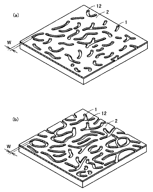
すなわち、図1および図3を参照して、本発明にかかるIII−V族化合物結晶の一の製造方法は、以下の工程により行なわれる。まず、図1(a)に示すように、基板1上に、蒸着法またはスパッタ法などの方法を用いて金属膜2を堆積する。次に、金属膜2をパタニーングする化合物の存在雰囲気下で熱処理することにより、図1(b)に示すように金属膜2が不定形にパターニングされて、図3(a)または図3(b)に示すような虫食い状の穴または溝12が形成され、穴または溝12の底部には基板1が露出する。次いで、図1(c)に示すように、前記熱処理後の虫食い状の穴または溝12が形成された金属膜2上に、たとえばHVPE(Hydride Vapor Phase Epitaxy:ハイドライド気相エピタキシャル成長)法などを用いてIII−V族化合物結晶4を成長させる。
【0012】
ここで、図3(a)および図3(b)は、いずれも金属膜2をパターニングする化合物の存在雰囲気下で熱処理することにより金属膜2に形成される虫食い状の穴または溝の代表的な形態を模式的に示したものである。なお、穴または溝が少ない場合には図3(a)の形態が多く、穴または溝が多くなるにつれて図3(b)の形態をとる傾向がある。
【0013】
かかる製造方法によると、図1を参照して、III−V族化合物結晶4は、基板1の結晶の格子定数などの情報を拾うことができるので、良好なIII−V族化合物結晶4が成長する。また、金属膜に虫食い状の穴または溝12のパターンが形成されることにより、III−V族化合物結晶4と金属膜2の間の応力が緩和され、III−V族化合物結晶4にクラックは発生しなくなる。また、III−V族化合物結晶は、高コストであるMOCVD法ではなく、上記HVPE法などのVPE(Vapor Phase Epitaxy:気相エピタキシャル成長)法により製造できるため、製造コストも低減できる。
【0014】
本発明にかかるIII−V族化合物結晶の製造方法においては、図1および図3を参照して、金属膜をパターニングする化合物の存在雰囲気下で熱処理することにより金属膜に形成される穴または溝の平均幅Wが2nm〜5000nmであり、基板全面積に対する穴または溝の領域面積の百分率である開口率が5%〜80%とすることが好ましい。穴または溝の平均幅Wが2nm未満であると基板まで達する穴または溝とならず基板の情報を読み取ることが困難となり、5000nmを越えるとIII−V族化合物結晶と基板の応力を緩和することが困難となる。かかる観点から、穴または溝の平均幅Wは、5nm〜1000nmであることがより好ましい。また、開口率が5%未満であるとIII−V族化合物結晶が基板と接触する面積が小さく基板の情報を読み取ることが難しくなり、80%を越えると金属膜のない部分が大きくなりすぎIII−V族化合物結晶と基板の応力を緩和することが難しくなる。かかる観点から、開口率は、10%〜50%であることがより好ましい。ここで、開口率とは、上記のように基板全面積に対する穴または溝の領域面積の百分率として、次式(1)によって定義される。
【0015】
開口率(%)=(穴または溝の領域面積)/(基板全面積)×100 (1)ここで、基板は、本発明の目的に反さない限り、成長させるIII−V族化合物結晶と同種、異種とを問わず広く用いることができる。たとえば、シリコン、サファイア、SiC、ZrB2またはIII−V族化合物が好ましい。前記列挙した化合物の結晶の格子定数は、III−V族化合物結晶の格子定数に近く、良質な結晶を得やすい。なお、基板とするIII−V化合物とその上に成長させるIII−V族化合物結晶とは、同一の化合物でなくともよい。
【0016】
また、金属膜は、特に制限はないが、パターニングを行ないやすいという観点から、チタン(Ti)またはバナジウム(V)を含有するものが好ましい。好ましいものとしてTi、Ti−Al、VまたはV−Alなどの金属または合金が挙げられる。
【0017】
金属膜の厚さは、特に制限はないが、10nm〜1000nmとすることが好ましい。10nm未満であるとパターニングの際に金属膜を残すことが難しくなり、1000nmを越えるとパターニングの際に基板を露出させることが難しくなる。かかる観点から、金属膜の厚さは、30nm〜500nmであることがより好ましい。
【0018】
金属膜をパターニングする化合物とは、この化合物の存在雰囲気下に金属膜を熱処理すると、金属膜に虫食い状の穴または溝を不定形にパターニングする化合物をいい、アンモニア(NH3)、窒素(N2)などが好ましいものとして挙げられる。
【0019】
金属膜をパターニングする化合物の存在雰囲気下で熱処理する際の熱処理条件は、800℃〜1200℃で0.5分間〜20分間行なうことが好ましい。熱処理温度が800℃未満または熱処理時間が0.5分間未満であると金属膜のパタニーングが不十分となり、熱処理温度が1200℃を越える場合または熱処理時間が20分間を越える場合には金属膜のパターニングが過剰となる。上記観点から、熱処理温度は900℃〜1100℃であることがより好ましく、熱処理時間は0.5分間〜10分間であることがより好ましい。
【0020】
上記の簡便でコストの低い製造方法により、良質なIII−V族化合物結晶が得られる。また、上記においてIII−V族化合物結晶がGaxAlyIn1-x-yN(0≦x≦1、0≦y≦1)である場合には、これらの結晶については、現在のところ他に特に有用な製造方法がないことから、極めて有用な製造方法となる。
【0021】
(実施形態2)
本発明にかかるIII−V族化合物結晶の別の製造方法は、図2を参照して、図2(a)に示すように基板1上に金属膜2を堆積する工程と、図2(b)に示すように前記金属膜2をパターニングする化合物の存在雰囲気下で熱処理する工程と、図2(c)に示すように前記熱処理後の金属膜2上にIII−V族化合物バッファ膜3を成長させる工程と、図2(d)に示すように前記III−V族化合物バッファ膜3上にIII−V族化合物結晶4を成長させる工程とを備えることを特徴とする。
【0022】
すなわち、図2および図3を参照して、本発明にかかるIII−V族化合物結晶の別の製造方法は、以下の工程により行なわれる。まず、図2(a)に示すように、基板1上に、蒸着法またはスパッタ法などの方法を用いて金属膜2を堆積する。次に、金属膜2をパタニーングする化合物の存在雰囲気下で熱処理することにより、図2(b)に示すように金属膜2が不定形にパターニングされて、図3(a)または図3(b)に示すような虫食い状の穴または溝12が形成され、穴または溝12の底部には基板1が露出する。
【0023】
次いで、図2(c)に示すように、前記熱処理後の虫食い状の穴または溝12が形成された金属膜2上に、たとえばHVPE法などを用いてIII−V族化合物バッファ膜3を成長させる。ここで、III−V族化合物バッファ膜3とは、結晶を成長させる場合に比べて低温で成長させたIII−V族化合物のアモルファス膜をいう。また、バッファ膜を形成するIII−V族化合物と、結晶を形成するIII−V族化合物とは、必ずしも同一の化学組成でなくともよいが、同一の化学組成を有することが、成長させる結晶の質を向上させる観点から好ましい。次いで、図2(d)に示すように、III−V族化合物バッファ膜3上に、たとえばHVPE法などを用いてIII−V族化合物結晶4を成長させる。
【0024】
上記実施形態2においては、虫食い状の穴または溝が形成された金属膜2上に形成されることによって、後にIII−V族化合物バッファ膜3上に形成されるIII−V族化合物結晶4と基板1の間の応力をより緩和することができる。また、III−V族化合物結晶4の成長の際には、基板1ではなく、III−V族化合物のアモルファス膜の情報を拾うため、不要な結晶情報が入らずより良質なIII−V族化合物結晶が得られる。
【0025】
【実施例】
さらに、上記実施形態1および実施形態2について、具体的な実施例に基づいて説明する。
【0026】
(実施例1)
実施形態1に基づいて、図1を参照して、図1(a)に示すように、基板1としてサファイア基板を用い、基板1上に蒸着法により金属膜2として金属Ti膜を30nm堆積した。次に、図1(b)に示すように、金属膜2をNH3雰囲気中1000℃で0.5分間熱処理した。降温後、SEM(Scanning Electron Microscope:走査型電子顕微鏡)で金属膜2の表面を観察すると、図3(a)に示すような虫食い状の穴または溝が見られ、穴または溝の平均幅Wは8nm、開口率は12%であった。さらに、図1(c)に示すように、原料にGaおよびNH3を用いたHVPE法により、1000℃で5時間かけてIII−V族化合物結晶4を成長させたところクラックのない結晶が得られた。得られた結晶は、XRD測定によりGaN結晶であり、XRDにおけるFWHM(Full Width Half Maximum;半値幅)は120arsecの良好な結晶であることがわかった。結果を表1に示す。
【0027】
(実施例2〜実施例9、参考例1〜参考例3)
表1に示す試験条件において、実施例1と同様の手順でIII−V族化合物結晶を成長させた。結果を表1にまとめた。
【0028】
【表1】
(実施例10)
実施形態2に基づいて、図2を参照して、図2(a)に示すように、基板1としてサファイア基板を用い、基板1上に蒸着法により金属膜2として金属Ti膜を200nm堆積した。次に、図2(b)に示すように、金属膜2をNH3雰囲気中1000℃で3分間熱処理した。降温後、SEM(Scanning Electron Microscope:走査型電子顕微鏡)で金属膜2の表面を観察すると、図3(a)に示すような虫食い状の穴または溝が見られ、穴または溝の平均幅Wは31nm、開口率は22%であった。次に、図2(c)に示すように、原料にGaおよびNH3を用いたHVPE法により、500℃で0.5時間かけてIII−V族化合物バッファ膜3を成長させた。さらに、図2(d)に示すように、原料にGaおよびNH3を用いたHVPE法により、1000℃で5時間かけてIII−V族化合物結晶4を成長させたところクラックのない結晶が得られた。得られた結晶は、XRD測定によりGaN結晶であり、XRDにおけるFWHM(Full Width Half Maximum;半値幅)は80arsecの良好な結晶であることがわかった。結果を表2に示す。
【0030】
(実施例11〜実施例14、参考例4〜参考例6)
表2に示す試験条件において、実施例10と同様の手順でIII−V族化合物結晶を成長させた。結果を表2にまとめた。
【0031】
【表2】
表1および表2から明らかなように、いずれの実施例においてもクラックの発生のない良質のIII−V族化合物結晶が得られた。また、たとえば、実施例3と実施例10または実施例8と実施例13を対比すると、結晶のXRD回折におけるFWHMが、それぞれ110arsecから80arsec、115arsecから90arsecと減少し、III−V族化合物結晶の結晶成長の前にバッファ膜成長を行なうことにより、結晶の質がさらに向上していることがわかる。
【0033】
今回開示された実施の形態および実施例はすべての点で例示であって制限的なものではないと考えられるべきである。本発明の範囲は、上記した説明でなくて特許請求の範囲によって示され、特許請求の範囲と均等の意味および範囲内のすべての変更が含まれることが意図される。
【0034】
【発明の効果】
上記のように、本発明によれば、基板上に金属膜を堆積する工程と、前記金属膜をパターニングする化合物の存在雰囲気下で熱処理する工程と、前記熱処理後の金属膜上にIII−V族化合物結晶を成長させる工程とを備えることにより、簡便でコストの低い製造法方法で、クラックを発生させることなく良質のIII−V族化合物結晶を得ることができる。
【図面の簡単な説明】
【図1】 本発明にかかるIII−V族化合物結晶の一の製造方法を説明する図である。
【図2】 本発明にかかるIII−V族化合物結晶の別の製造方法を説明する図である。
【図3】 (a)は金属膜に形成される穴または溝の代表的な一の形態を示す模式図であり、(b)は金属膜に形成される穴または溝の代表的な別の形態を示す模式図である。
【符号の説明】
1 基板、2 金属膜、3 III−V族化合物バッファ膜、4 III−V族化合物結晶、12 穴または溝。[0001]
BACKGROUND OF THE INVENTION
The present invention relates to a group III-V compound crystal and a method for producing the same, and more particularly to a method for producing a good group III-V compound crystal without generating cracks even when various substrates are used.
[0002]
[Prior art]
When a group III-V compound crystal such as a GaN crystal is grown on a sapphire substrate, a silicon (Si) substrate, or the like, which is a substrate different from the crystal material, the crystal and Stress occurs between the substrates, warping and cracks occur, and a good III-V group compound crystal cannot be obtained.
[0003]
Therefore, after depositing a silicon oxide (SiO 2 or the like) film on the sapphire substrate and patterning the silicon oxide film by a photolithography method or the like, a group III-V compound crystal is grown, thereby forming a gap between the crystal and the substrate. A method of relieving the stress is being carried out. However, this method has a problem that the silicon oxide film needs to be patterned and the manufacturing cost is high.
[0004]
In addition, a GaN layer is grown on a sapphire substrate by MOCVD (Metal Organic Chemical Vapor Deposition) method, a metal film is deposited thereon, and then heat treatment is performed to form the GaN layer. A method of growing a GaN crystal after forming a void has been proposed (see, for example, Patent Document 1). However, this method has a problem that the growth of the GaN layer by the MOCDV method is essential, and the manufacturing cost is extremely high.
[0005]
Furthermore, a method of growing a GaN crystal after depositing a metal film on a sapphire substrate or the like has been proposed (see, for example, Patent Document 2). However, this method has a problem in that the characteristics of the obtained GaN crystal are deteriorated because the GaN crystal is grown on a metal film having a lattice constant different from that of the GaN crystal.
[0006]
[Patent Document 1]
Japanese Patent Laid-Open No. 2002-343728
[Patent Document 2]
Japanese Patent Laid-Open No. 2002-284600
[Problems to be solved by the invention]
In order to solve the above problems, an object of the present invention is to provide a high-quality group III-V compound crystal obtained by a simple and low-cost production method and a production method thereof.
[0009]
[Means for Solving the Problems]
In order to achieve the above object, a method for producing a group III-V compound according to the present invention deposits a metal film having a thickness of 10 nm to 1000 nm containing titanium or vanadium on a silicon, sapphire, SiC or ZrB 2 substrate. step and a step of heat treating the metal film of 0.5 minutes to 20 minutes in the presence atmosphere of 800 ° C. to 1200 ° C. ammonia or nitrogen, on the metal film after the heat treatment Ga x Al y in 1-xy N ( And a step of growing a group III-V compound crystal having a composition of 0 ≦ x ≦ 1, 0 ≦ y ≦ 1) . Further, after the heat treatment step, a step of growing a group III-V compound buffer film on the metal film after the heat treatment, Ga in the group III-V compound buffer film on the x Al y In 1-xy N (0 And a step of growing a group III-V compound crystal having a composition of ≦ x ≦ 1, 0 ≦ y ≦ 1) .
[0010]
DETAILED DESCRIPTION OF THE INVENTION
(Embodiment 1)
One method for producing a group III-V compound crystal according to the present invention is described with reference to FIG. 1, in which a
[0011]
That is, with reference to FIG. 1 and FIG. 3, one manufacturing method of the III-V compound crystal concerning this invention is performed by the following processes. First, as shown in FIG. 1A, a
[0012]
Here, both FIG. 3A and FIG. 3B are representative of worm-like holes or grooves formed in the
[0013]
According to this manufacturing method, referring to FIG. 1, since the III-V
[0014]
In the method for producing a group III-V compound crystal according to the present invention, referring to FIG. 1 and FIG. 3, holes or grooves formed in the metal film by heat-treating the metal film in the presence atmosphere of the compound for patterning. It is preferable that the average width W is 2 nm to 5000 nm, and the aperture ratio, which is the percentage of the area of the hole or groove with respect to the total area of the substrate, is 5% to 80%. If the average width W of the holes or grooves is less than 2 nm, it will not be a hole or groove reaching the substrate and it will be difficult to read information on the substrate, and if it exceeds 5000 nm, the stress of the III-V group compound crystal and the substrate will be relaxed It becomes difficult. From this viewpoint, the average width W of the holes or grooves is more preferably 5 nm to 1000 nm. If the aperture ratio is less than 5%, the area where the III-V compound crystal is in contact with the substrate is small and it is difficult to read information on the substrate. If it exceeds 80%, the portion without the metal film becomes too large. It becomes difficult to relieve stress between the group V compound crystal and the substrate. From this viewpoint, the aperture ratio is more preferably 10% to 50%. Here, the aperture ratio is defined by the following expression (1) as a percentage of the area of the hole or groove with respect to the total area of the substrate as described above.
[0015]
Opening ratio (%) = (region area of hole or groove) / (total area of substrate) × 100 (1) Here, unless the object of the present invention is contrary to the object of the present invention, It can be widely used regardless of the same type or different types. For example, silicon, sapphire, SiC, ZrB 2 or III-V group compounds are preferred. The lattice constants of the crystals of the above listed compounds are close to the lattice constants of III-V group compound crystals, and it is easy to obtain good quality crystals. Note that the III-V compound used as the substrate and the III-V group compound crystal grown thereon may not be the same compound.
[0016]
Further, the metal film is not particularly limited, but preferably contains titanium (Ti) or vanadium (V) from the viewpoint of easy patterning. Preferable examples include metals or alloys such as Ti, Ti—Al, V or V—Al.
[0017]
The thickness of the metal film is not particularly limited, but is preferably 10 nm to 1000 nm. If it is less than 10 nm, it is difficult to leave a metal film during patterning, and if it exceeds 1000 nm, it is difficult to expose the substrate during patterning. From this viewpoint, the thickness of the metal film is more preferably 30 nm to 500 nm.
[0018]
A compound for patterning a metal film refers to a compound that patterns a worm-eaten hole or groove in an amorphous shape when the metal film is heat-treated in the presence of the compound, and includes ammonia (NH 3 ), nitrogen (N 2 ) is preferable.
[0019]
The heat treatment conditions for the heat treatment in the presence of the compound for patterning the metal film are preferably 800 ° C. to 1200 ° C. for 0.5 minutes to 20 minutes. When the heat treatment temperature is less than 800 ° C. or the heat treatment time is less than 0.5 minutes, the patterning of the metal film becomes insufficient. When the heat treatment temperature exceeds 1200 ° C. or when the heat treatment time exceeds 20 minutes, the patterning of the metal film is performed. Becomes excessive. From the above viewpoint, the heat treatment temperature is more preferably 900 ° C. to 1100 ° C., and the heat treatment time is more preferably 0.5 minutes to 10 minutes.
[0020]
Good quality III-V compound crystals can be obtained by the above simple and low cost production method. Further, when the group III-V compound crystal is Ga x Al y In 1-xy N (0 ≦ x ≦ 1,0 ≦ y ≦ 1) in the above, for these crystals, the presently Other Since there is no particularly useful production method, it is a very useful production method.
[0021]
(Embodiment 2)
Another method for producing a group III-V compound crystal according to the present invention is a process of depositing a
[0022]
That is, with reference to FIG. 2 and FIG. 3, another manufacturing method of the group III-V compound crystal concerning this invention is performed by the following processes. First, as shown in FIG. 2A, a
[0023]
Next, as shown in FIG. 2C, the III-V compound buffer film 3 is grown on the
[0024]
In the second embodiment, the III-
[0025]
【Example】
Further,
[0026]
Example 1
Based on the first embodiment, referring to FIG. 1, as shown in FIG. 1A, a sapphire substrate is used as the
[0027]
(Example 2 to Example 9, Reference Example 1 to Reference Example 3 )
Under the test conditions shown in Table 1, III-V compound crystals were grown in the same procedure as in Example 1. The results are summarized in Table 1.
[0028]
[Table 1]
(Example 10 )
Based on the second embodiment, referring to FIG. 2, as shown in FIG. 2A, a sapphire substrate is used as the
[0030]
(Example 11 to Example 14, Reference Example 4 to Reference Example 6 )
Under the test conditions shown in Table 2, group III-V compound crystals were grown in the same procedure as in Example 10 . The results are summarized in Table 2.
[0031]
[Table 2]
As is clear from Tables 1 and 2, a good-quality III-V compound crystal free from cracks was obtained in any of the examples. Further, for example, when Example 3 and Example 10 or Example 8 and Example 13 are compared, the FWHM in the XRD diffraction of the crystal decreases from 110 to 80 asec and from 115 to 90 asec, respectively. It can be seen that crystal quality is further improved by performing buffer film growth before crystal growth.
[0033]
It should be understood that the embodiments and examples disclosed herein are illustrative and non-restrictive in every respect. The scope of the present invention is defined by the terms of the claims, rather than the description above, and is intended to include any modifications within the scope and meaning equivalent to the terms of the claims.
[0034]
【The invention's effect】
As described above, according to the present invention, a step of depositing a metal film on a substrate, a step of heat-treating in the presence of a compound for patterning the metal film, and III-V on the metal film after the heat treatment are performed. And a step of growing a group compound crystal, a high-quality group III-V compound crystal can be obtained without generating cracks by a simple and low-cost production method.
[Brief description of the drawings]
BRIEF DESCRIPTION OF DRAWINGS FIG. 1 is a diagram for explaining a method for producing a group III-V compound crystal according to the present invention.
FIG. 2 is a diagram for explaining another method for producing a group III-V compound crystal according to the present invention.
FIG. 3A is a schematic view showing one typical form of a hole or groove formed in a metal film, and FIG. 3B is another typical hole or groove formed in a metal film. It is a schematic diagram which shows a form.
[Explanation of symbols]
1 substrate, 2 metal film, 3 III-V compound buffer film, 4 III-V compound crystal, 12 holes or grooves.
Claims (3)
Priority Applications (11)
| Application Number | Priority Date | Filing Date | Title |
|---|---|---|---|
| JP2003129829A JP4457576B2 (en) | 2003-05-08 | 2003-05-08 | Group III-V compound crystal and method for producing the same |
| EP04725190A EP1522612A4 (en) | 2003-05-08 | 2004-04-01 | COMPOUND III-V SEMICONDUCTOR CRYSTAL AND PROCESS FOR PRODUCING THE SAME |
| CNB2004800006464A CN1318661C (en) | 2003-05-08 | 2004-04-01 | III-V group crystal and production method thereof |
| PCT/JP2004/004811 WO2004099472A1 (en) | 2003-05-08 | 2004-04-01 | Iii-v compound semiconductor crystal and method for production thereof |
| CN200710102802.3A CN101071794B (en) | 2003-05-08 | 2004-04-01 | Group III-V crystals and methods for their production |
| US10/521,060 US7297625B2 (en) | 2003-05-08 | 2004-04-01 | Group III-V crystal and manufacturing method thereof |
| TW093109623A TW200503076A (en) | 2003-05-08 | 2004-04-07 | III-V compound semiconductor crystal and method for production thereof |
| US11/871,162 US7485484B2 (en) | 2003-05-08 | 2007-10-12 | Group III-V crystal |
| US12/188,214 US20080299748A1 (en) | 2003-05-08 | 2008-08-08 | Group III-V Crystal |
| US12/617,733 US8134223B2 (en) | 2003-05-08 | 2009-11-13 | III-V compound crystal and semiconductor electronic circuit element |
| US13/368,329 US8304334B2 (en) | 2003-05-08 | 2012-02-07 | III-V compound crystal and semiconductor electronic circuit element |
Applications Claiming Priority (1)
| Application Number | Priority Date | Filing Date | Title |
|---|---|---|---|
| JP2003129829A JP4457576B2 (en) | 2003-05-08 | 2003-05-08 | Group III-V compound crystal and method for producing the same |
Related Child Applications (1)
| Application Number | Title | Priority Date | Filing Date |
|---|---|---|---|
| JP2009177767A Division JP2009292718A (en) | 2009-07-30 | 2009-07-30 | Group iii-v compound crystal-containing material and method for producing group iii-v compound crystal |
Publications (2)
| Publication Number | Publication Date |
|---|---|
| JP2004331453A JP2004331453A (en) | 2004-11-25 |
| JP4457576B2 true JP4457576B2 (en) | 2010-04-28 |
Family
ID=33432087
Family Applications (1)
| Application Number | Title | Priority Date | Filing Date |
|---|---|---|---|
| JP2003129829A Expired - Fee Related JP4457576B2 (en) | 2003-05-08 | 2003-05-08 | Group III-V compound crystal and method for producing the same |
Country Status (6)
| Country | Link |
|---|---|
| US (3) | US7297625B2 (en) |
| EP (1) | EP1522612A4 (en) |
| JP (1) | JP4457576B2 (en) |
| CN (2) | CN101071794B (en) |
| TW (1) | TW200503076A (en) |
| WO (1) | WO2004099472A1 (en) |
Cited By (3)
| Publication number | Priority date | Publication date | Assignee | Title |
|---|---|---|---|---|
| KR20170028962A (en) | 2014-08-12 | 2017-03-14 | 티디케이가부시기가이샤 | Alumina substrate |
| KR20170106375A (en) | 2015-03-23 | 2017-09-20 | 티디케이가부시기가이샤 | Alumina substrate |
| US10337120B2 (en) | 2014-08-12 | 2019-07-02 | Tdk Corporation | Alumina substrate |
Families Citing this family (25)
| Publication number | Priority date | Publication date | Assignee | Title |
|---|---|---|---|---|
| JP4457576B2 (en) * | 2003-05-08 | 2010-04-28 | 住友電気工業株式会社 | Group III-V compound crystal and method for producing the same |
| JP4396816B2 (en) | 2003-10-17 | 2010-01-13 | 日立電線株式会社 | Group III nitride semiconductor substrate and manufacturing method thereof |
| JP2007027417A (en) * | 2005-07-15 | 2007-02-01 | Sanken Electric Co Ltd | Nitride semiconductor device and manufacturing method thereof |
| JP5057774B2 (en) * | 2006-12-26 | 2012-10-24 | 京セラ株式会社 | LIGHT EMITTING ELEMENT AND LIGHTING DEVICE |
| CN101796212B (en) * | 2007-09-03 | 2014-04-09 | 学校法人上智学院 | III nitride structure and method for manufacturing III nitride semiconductor fine columnar crystal |
| US20090114274A1 (en) | 2007-11-02 | 2009-05-07 | Fritzemeier Leslie G | Crystalline thin-film photovoltaic structures |
| JP2010042981A (en) | 2008-07-17 | 2010-02-25 | Sumitomo Electric Ind Ltd | METHOD FOR PRODUCING AlGaN BULK CRYSTAL AND METHOD FOR PRODUCING AlGaN SUBSTRATE |
| US8803189B2 (en) * | 2008-08-11 | 2014-08-12 | Taiwan Semiconductor Manufacturing Company, Ltd. | III-V compound semiconductor epitaxy using lateral overgrowth |
| WO2010088366A1 (en) | 2009-01-28 | 2010-08-05 | Wakonda Technologies, Inc. | Large-grain crystalline thin-film structures and devices and methods for forming the same |
| US8507304B2 (en) | 2009-07-17 | 2013-08-13 | Applied Materials, Inc. | Method of forming a group III-nitride crystalline film on a patterned substrate by hydride vapor phase epitaxy (HVPE) |
| US20110027973A1 (en) * | 2009-07-31 | 2011-02-03 | Applied Materials, Inc. | Method of forming led structures |
| US8148241B2 (en) * | 2009-07-31 | 2012-04-03 | Applied Materials, Inc. | Indium surfactant assisted HVPE of high quality gallium nitride and gallium nitride alloy films |
| JP2012054364A (en) * | 2010-08-31 | 2012-03-15 | Nobuyuki Akiyama | Manufacturing method of silicon thin film, manufacturing method of silicon thin film solar cell, silicon thin film, silicon thin film solar cell |
| KR101207412B1 (en) * | 2011-06-20 | 2012-12-04 | 삼성코닝정밀소재 주식회사 | Gan substrate and method for maufacturing the same |
| JP6051524B2 (en) * | 2012-01-18 | 2016-12-27 | セイコーエプソン株式会社 | Semiconductor substrate and semiconductor substrate manufacturing method |
| JP2013203617A (en) * | 2012-03-29 | 2013-10-07 | Ngk Insulators Ltd | Method for manufacturing group 13 element nitride crystal, and laminate |
| CN103814160B (en) * | 2012-08-30 | 2018-09-14 | 日本碍子株式会社 | Composite substrate, method for producing same, method for producing functional layer composed of nitride of group 13 elements, and functional element |
| JP2014067869A (en) * | 2012-09-26 | 2014-04-17 | Nobuyuki Akiyama | Manufacturing method of hetero-epitaxial single crystal, manufacturing method of heterojunction solar cell, hetero-epitaxial single crystal, and heterojunction solar cell |
| CN105264674B (en) * | 2013-12-20 | 2019-01-18 | 华为技术有限公司 | Semiconductor device and method of making semiconductor device |
| CN104716241B (en) * | 2015-03-16 | 2018-10-16 | 映瑞光电科技(上海)有限公司 | A kind of LED structure and preparation method thereof |
| CN105826438B (en) * | 2016-06-01 | 2018-05-08 | 安徽三安光电有限公司 | A kind of light emitting diode with metal buffer layer and preparation method thereof |
| CN108736317B (en) * | 2018-05-15 | 2021-01-12 | 深圳市光脉电子有限公司 | Light emitting diode epitaxial structure and matrix type laser device thereof |
| US11823900B2 (en) | 2018-10-10 | 2023-11-21 | The Johns Hopkins University | Method for printing wide bandgap semiconductor materials |
| US11056338B2 (en) | 2018-10-10 | 2021-07-06 | The Johns Hopkins University | Method for printing wide bandgap semiconductor materials |
| CN110120448B (en) * | 2019-05-07 | 2021-05-25 | 厦门大学 | Nitride LED manufacturing method based on metal mask substrate |
Family Cites Families (20)
| Publication number | Priority date | Publication date | Assignee | Title |
|---|---|---|---|---|
| US5868837A (en) * | 1997-01-17 | 1999-02-09 | Cornell Research Foundation, Inc. | Low temperature method of preparing GaN single crystals |
| JP3934320B2 (en) * | 1997-03-13 | 2007-06-20 | 日本電気株式会社 | GaN-based semiconductor device and manufacturing method thereof |
| TW490441B (en) | 1998-06-12 | 2002-06-11 | Rohm & Haas | Lithium manganate composition |
| CN1077607C (en) * | 1998-11-03 | 2002-01-09 | 南京大学 | Method and installation for GaN growth by light radiation-heated metallic organic chemical gas-state deposition |
| JP3470623B2 (en) * | 1998-11-26 | 2003-11-25 | ソニー株式会社 | Method for growing nitride III-V compound semiconductor, method for manufacturing semiconductor device, and semiconductor device |
| JP3305310B1 (en) | 1998-12-09 | 2002-07-22 | 松下電器産業株式会社 | Temperature measurement method |
| JP3929657B2 (en) * | 1999-09-29 | 2007-06-13 | 株式会社リコー | Crystal growth method and group III nitride crystal production method |
| JP3519641B2 (en) | 1999-08-18 | 2004-04-19 | シャープ株式会社 | Semiconductor device having gold wiring and method of manufacturing the same |
| JP2001223165A (en) | 2000-02-10 | 2001-08-17 | Hitachi Cable Ltd | Nitride semiconductor and manufacturing method thereof |
| JP2002270516A (en) * | 2001-03-07 | 2002-09-20 | Nec Corp | Method of growing group III nitride semiconductor, group III nitride semiconductor film, and semiconductor device using the same |
| JP2002280314A (en) * | 2001-03-22 | 2002-09-27 | Toyoda Gosei Co Ltd | Method of manufacturing group III nitride compound semiconductor and group III nitride compound semiconductor device based thereon |
| JP2003007616A (en) | 2001-03-23 | 2003-01-10 | Matsushita Electric Ind Co Ltd | Method for manufacturing semiconductor film |
| JP2002284600A (en) | 2001-03-26 | 2002-10-03 | Hitachi Cable Ltd | Gallium nitride crystal substrate manufacturing method and gallium nitride crystal substrate |
| JP3631724B2 (en) * | 2001-03-27 | 2005-03-23 | 日本電気株式会社 | Group III nitride semiconductor substrate and manufacturing method thereof |
| US6939730B2 (en) * | 2001-04-24 | 2005-09-06 | Sony Corporation | Nitride semiconductor, semiconductor device, and method of manufacturing the same |
| JP4575616B2 (en) | 2001-04-26 | 2010-11-04 | ルネサスエレクトロニクス株式会社 | Semiconductor device and manufacturing method thereof |
| JP3886341B2 (en) | 2001-05-21 | 2007-02-28 | 日本電気株式会社 | Method for manufacturing gallium nitride crystal substrate and gallium nitride crystal substrate |
| CN1167140C (en) * | 2002-05-17 | 2004-09-15 | 清华大学 | Substrate processing method for high-brightness GaN-based light-emitting diode epitaxial wafer |
| CN1174470C (en) * | 2002-05-31 | 2004-11-03 | 南京大学 | Method for growing high-quality GaN thin films by lateral epitaxial growth |
| JP4457576B2 (en) * | 2003-05-08 | 2010-04-28 | 住友電気工業株式会社 | Group III-V compound crystal and method for producing the same |
-
2003
- 2003-05-08 JP JP2003129829A patent/JP4457576B2/en not_active Expired - Fee Related
-
2004
- 2004-04-01 CN CN200710102802.3A patent/CN101071794B/en not_active Expired - Fee Related
- 2004-04-01 EP EP04725190A patent/EP1522612A4/en not_active Withdrawn
- 2004-04-01 US US10/521,060 patent/US7297625B2/en not_active Expired - Fee Related
- 2004-04-01 CN CNB2004800006464A patent/CN1318661C/en not_active Expired - Fee Related
- 2004-04-01 WO PCT/JP2004/004811 patent/WO2004099472A1/en not_active Ceased
- 2004-04-07 TW TW093109623A patent/TW200503076A/en not_active IP Right Cessation
-
2007
- 2007-10-12 US US11/871,162 patent/US7485484B2/en not_active Expired - Fee Related
-
2008
- 2008-08-08 US US12/188,214 patent/US20080299748A1/en not_active Abandoned
Cited By (5)
| Publication number | Priority date | Publication date | Assignee | Title |
|---|---|---|---|---|
| KR20170028962A (en) | 2014-08-12 | 2017-03-14 | 티디케이가부시기가이샤 | Alumina substrate |
| US10294585B2 (en) | 2014-08-12 | 2019-05-21 | Tdk Corporation | Alumina substrate |
| US10337120B2 (en) | 2014-08-12 | 2019-07-02 | Tdk Corporation | Alumina substrate |
| KR20170106375A (en) | 2015-03-23 | 2017-09-20 | 티디케이가부시기가이샤 | Alumina substrate |
| US10458041B2 (en) | 2015-03-23 | 2019-10-29 | Tdk Corporation | Alumina substrate |
Also Published As
| Publication number | Publication date |
|---|---|
| EP1522612A4 (en) | 2008-09-03 |
| US20080299748A1 (en) | 2008-12-04 |
| CN1697895A (en) | 2005-11-16 |
| CN101071794B (en) | 2010-09-01 |
| CN101071794A (en) | 2007-11-14 |
| US7485484B2 (en) | 2009-02-03 |
| US7297625B2 (en) | 2007-11-20 |
| US20080038580A1 (en) | 2008-02-14 |
| EP1522612A1 (en) | 2005-04-13 |
| WO2004099472A1 (en) | 2004-11-18 |
| TWI295481B (en) | 2008-04-01 |
| CN1318661C (en) | 2007-05-30 |
| JP2004331453A (en) | 2004-11-25 |
| US20050227472A1 (en) | 2005-10-13 |
| TW200503076A (en) | 2005-01-16 |
Similar Documents
| Publication | Publication Date | Title |
|---|---|---|
| JP4457576B2 (en) | Group III-V compound crystal and method for producing the same | |
| JP4117156B2 (en) | Method for manufacturing group III nitride semiconductor substrate | |
| KR100682880B1 (en) | Crystal growth method | |
| JP3886341B2 (en) | Method for manufacturing gallium nitride crystal substrate and gallium nitride crystal substrate | |
| WO2010110489A9 (en) | Substrate for growing group-iii nitride semiconductors, epitaxial substrate for group-iii nitride semiconductors, group-iii nitride semiconductor element, stand-alone substrate for group-iii nitride semiconductors, and methods for manufacturing the preceding | |
| JP2008034834A6 (en) | Nitride single crystal growth method on silicon substrate, nitride semiconductor light emitting device using the same, and manufacturing method thereof | |
| KR20090081879A (en) | Method of manufacturing nitride semiconductor substrate | |
| JP4301592B2 (en) | Manufacturing method of substrate with nitride semiconductor layer | |
| KR101358541B1 (en) | Ⅲ-nitride semiconductor growth substrate, ⅲ-nitride semiconductor epitaxial substrate, ⅲ-nitride semiconductor element, ⅲ-nitride semiconductor freestanding substrate, and method for fabricating these | |
| JP4768759B2 (en) | Group III nitride semiconductor substrate | |
| WO2015198492A1 (en) | Epitaxial wafer manufacturing method and epitaxial wafer | |
| JP7800516B2 (en) | Laminate | |
| JP2009292718A (en) | Group iii-v compound crystal-containing material and method for producing group iii-v compound crystal | |
| KR101635530B1 (en) | Method for the growth of nitride semiconductor crystal with voids and Method for the manufacturing of nitride semiconductor substrate thereof | |
| JP5684551B2 (en) | Group III nitride semiconductor growth substrate, group III nitride semiconductor epitaxial substrate, group III nitride semiconductor device, group III nitride semiconductor free-standing substrate, and methods of manufacturing the same | |
| CN116479400A (en) | A method for improving the crystal quality of Al-containing nitride semiconductor materials | |
| JP4236122B2 (en) | Manufacturing method of semiconductor substrate | |
| JP2010278470A (en) | Substrate for growing group-iii nitride semiconductor, epitaxial substrate for group-iii nitride semiconductor, group-iii nitride semiconductor element, stand-alone substrate for group-iii nitride semiconductor, and methods for manufacturing the same | |
| JP2010132550A (en) | Method of manufacturing nitride semiconductor substrate, and nitride semiconductor substrate |
Legal Events
| Date | Code | Title | Description |
|---|---|---|---|
| A621 | Written request for application examination |
Free format text: JAPANESE INTERMEDIATE CODE: A621 Effective date: 20051019 |
|
| A131 | Notification of reasons for refusal |
Free format text: JAPANESE INTERMEDIATE CODE: A131 Effective date: 20080909 |
|
| A521 | Request for written amendment filed |
Free format text: JAPANESE INTERMEDIATE CODE: A523 Effective date: 20081105 |
|
| A131 | Notification of reasons for refusal |
Free format text: JAPANESE INTERMEDIATE CODE: A131 Effective date: 20090602 |
|
| A521 | Request for written amendment filed |
Free format text: JAPANESE INTERMEDIATE CODE: A523 Effective date: 20090730 |
|
| A131 | Notification of reasons for refusal |
Free format text: JAPANESE INTERMEDIATE CODE: A131 Effective date: 20090929 |
|
| A521 | Request for written amendment filed |
Free format text: JAPANESE INTERMEDIATE CODE: A523 Effective date: 20091124 |
|
| TRDD | Decision of grant or rejection written | ||
| A01 | Written decision to grant a patent or to grant a registration (utility model) |
Free format text: JAPANESE INTERMEDIATE CODE: A01 Effective date: 20100119 |
|
| A01 | Written decision to grant a patent or to grant a registration (utility model) |
Free format text: JAPANESE INTERMEDIATE CODE: A01 |
|
| A61 | First payment of annual fees (during grant procedure) |
Free format text: JAPANESE INTERMEDIATE CODE: A61 Effective date: 20100201 |
|
| R150 | Certificate of patent or registration of utility model |
Free format text: JAPANESE INTERMEDIATE CODE: R150 |
|
| FPAY | Renewal fee payment (event date is renewal date of database) |
Free format text: PAYMENT UNTIL: 20130219 Year of fee payment: 3 |
|
| FPAY | Renewal fee payment (event date is renewal date of database) |
Free format text: PAYMENT UNTIL: 20140219 Year of fee payment: 4 |
|
| LAPS | Cancellation because of no payment of annual fees |