JP3929657B2 - Crystal growth method and group III nitride crystal production method - Google Patents
Crystal growth method and group III nitride crystal production method Download PDFInfo
- Publication number
- JP3929657B2 JP3929657B2 JP27704599A JP27704599A JP3929657B2 JP 3929657 B2 JP3929657 B2 JP 3929657B2 JP 27704599 A JP27704599 A JP 27704599A JP 27704599 A JP27704599 A JP 27704599A JP 3929657 B2 JP3929657 B2 JP 3929657B2
- Authority
- JP
- Japan
- Prior art keywords
- group iii
- crystal
- iii nitride
- crystal growth
- melt
- Prior art date
- Legal status (The legal status is an assumption and is not a legal conclusion. Google has not performed a legal analysis and makes no representation as to the accuracy of the status listed.)
- Expired - Lifetime
Links
Images


Description
【0001】
【発明の属する技術分野】
本発明は、結晶成長方法および結晶成長装置およびIII族窒化物結晶および半導体デバイスに関する。
【0002】
【従来の技術】
現在、紫〜青〜緑色光源として用いられているInGaAlN系(III族窒化物)デバイスは、そのほとんどがサファイアあるいはSiC基板上にMO−CVD法(有機金属化学気相成長法)やMBE法(分子線結晶成長法)等を用いた結晶成長により作製されている。サファイアやSiCを基板として用いる場合には、III族窒化物との熱膨張係数差や格子定数差が大きいことに起因する結晶欠陥が多くなる。このために、デバイス特性が悪く、例えば発光デバイスの寿命を長くすることが困難であったり、動作電力が大きくなったりするという問題がある。
【0003】
さらに、サファイア基板の場合には絶縁性であるために、従来の発光デバイスのように基板側からの電極取り出しが不可能であり、結晶成長した窒化物半導体表面側からの電極取り出しが必要となる。その結果、デバイス面積が大きくなり、高コストにつながるという問題がある。また、サファイア基板上に作製したIII族窒化物半導体デバイスは劈開によるチップ分離が困難であり、レーザダイオード(LD)で必要とされる共振器端面を劈開で得ることが容易ではない。このため、現在はドライエッチングによる共振器端面形成や、あるいはサファイア基板を100μm以下の厚さまで研磨した後に、劈開に近い形での共振器端面形成を行なっている。この場合にも、従来のLDのような共振器端面とチップ分離を単一工程で、容易に行なうことが不可能であり、工程の複雑化ひいてはコスト高につながる。
【0004】
この問題を解決するために、サファイア基板上にIII族窒化物半導体膜を選択横方向成長やその他の工夫を行なうことで、結晶欠陥を低減させることが提案されている。
【0005】
例えば文献「Japanese Journal of Applied Physics Vol.36 (1997) Part 2, No.12A, L1568-1571」(以下、第1の従来技術と称す)には、図6に示すようなレーザダイオード(LD)が示されている。図6のレーザダイオードは、MO−VPE(有機金属気相成長)装置にてサファイア基板1上にGaN低温バッファ層2とGaN層3を順次成長した後に、選択成長用のSiO2マスク4を形成する。このSiO2マスク4は、別のCVD(化学気相堆積)装置にてSiO2膜を堆積した後に、フォトリソグラフィー,エッチング工程を経て形成される。次に、このSiO2マスク4上に再度、MO−VPE装置にて20μmの厚さのGaN膜3’を成長することで、横方向にGaNが選択成長し、選択横方向成長を行なわない場合に比較して結晶欠陥を低減させている。さらに、その上層に形成されている変調ドープ歪み超格子層(MD−SLS)5を導入することで、活性層6へ結晶欠陥が延びることを防いでいる。この結果、選択横方向成長および変調ドープ歪み超格子層を用いない場合に比較して、デバイス寿命を長くすることが可能となる。
【0006】
この第1の従来技術の場合には、サファイア基板上にGaN膜を選択横方向成長しない場合に比べて、結晶欠陥を低減させることが可能となるが、サファイア基板を用いることによる、絶縁性と劈開に関する前述の問題は依然として残っている。さらには、SiO2マスク形成工程を挟んで、MO−VPE装置による結晶成長が2回必要となり、工程が複雑化するという問題が新たに生じる。
【0007】
また、別の方法として、例えば文献「Applied Physics Letters, Vol.73, No.6, P832-834 (1998)」(以下、第2の従来技術と称す)には、GaN厚膜基板を応用することが提案されている。この第2の従来技術では、前述の第1の従来技術の20μmの選択横方向成長後に、H−VPE(ハイドライド気相成長)装置にて200μmのGaN厚膜を成長し、その後に、この厚膜成長したGaN膜を150μmの厚さになるように、サファイア基板側から研磨することにより、GaN基板を作製する。このGaN基板上にMO−VPE装置を用いて、LDデバイスとして必要な結晶成長を順次行ない、LDデバイスを作製する。この結果、結晶欠陥の問題に加えて、サファイア基板を用いることによる絶縁性と劈開に関する前述の問題点を解決することが可能となる。
【0008】
しかしながら、第2の従来技術は、第1の従来技術よりもさらに工程が複雑になっており、より一層のコスト高となる。また、第2の従来技術の方法で200μmものGaN厚膜を成長させる場合には、基板であるサファイアとの格子定数差および熱膨張係数差に伴う応力が大きくなり、基板の反りやクラックが生じるという問題が新たに発生する。
【0009】
この問題を回避するために、特開平10−256662号では、厚膜成長する元の基板(サファイアとスピネル)の厚さを1mm以上とすることが提案されている。このように、厚さ1mm以上の基板を用いることにより、200μmの厚膜のGaN膜を成長させても、基板の反りやクラックを生じさせないようにしている。しかしながら、このように厚い基板は、基板自体のコストが高く、また研磨に多くの時間を費やす必要があり、研磨工程のコストアップにつながる。すなわち、厚い基板を用いる場合には、薄い基板を用いる場合に比べて、コストが高くなる。また、厚い基板を用いる場合には、厚膜のGaN膜を成長した後には基板の反りやクラックが生じないが、研磨の工程で応力緩和し、研磨途中で反りやクラックが発生する。このため、厚い基板を用いても容易に、結晶品質の高いGaN基板を大面積化で作製することはできない。
【0010】
一方、文献「Journal of Crystal Growth, Vol.189/190, p.153-158 (1998)」(以下、第3の従来技術と称す)には、GaNのバルク結晶を成長させ、それをホモエピタキシャル基板として用いることが提案されている。この技術は、1400〜1700℃の高温、および数10kbarもの超高圧の窒素圧力中で、液体GaからGaNを結晶成長させる手法となっている。この場合には、このバルク成長したGaN基板を用いて、デバイスに必要なIII族窒化物半導体膜を成長することが可能となる。従って、第1および第2の従来技術のように工程を複雑化させることなく、GaN基板を提供できる。
【0011】
しかしながら、第3の従来技術では、高温,高圧中での結晶成長が必要となり、それに耐えうる反応容器が極めて高価になるという問題がある。加えて、このような成長方法をもってしても、得られる結晶の大きさは高々1cm程度であり、デバイスを実用化するには小さ過ぎるという問題がある。
【0012】
この高温,高圧中でのGaN結晶成長の問題点を解決する手法として、文献「Chemistry of Materials Vol.9 (1997) p.413-416」(以下、第4の従来技術と称す)には、Naをフラックスとして用いたGaN結晶成長方法が提案されている。この方法は、フラックスとしてのアジ化ナトリウム(NaN3)と金属Gaとを原料として、ステンレス製の反応容器(容器内寸法;内径=7.5mm、長さ=100mm)に窒素雰囲気で封入し、その反応容器を600〜800℃の温度で24〜100時間保持することにより、GaN結晶を成長させるものである。この第4の従来技術の場合には、600〜800℃程度の比較的低温での結晶成長が可能であり、容器内圧力も高々100kg/cm2程度と第3の従来技術に比較して圧力を低くできる点が特徴である。しかし、この方法の問題点としては、得られる結晶の大きさが1mmに満たない程度に小さい点である。この程度の大きさではデバイスを実用化するには第3の従来技術の場合と同様に小さすぎる。
【0013】
【発明が解決しようとする課題】
本発明は、第1や第2の従来技術の問題点である工程を複雑化させることなく、第3の従来技術の問題点である高価な反応容器を用いることなく、かつ第3や第4の従来技術の問題点である結晶の大きさが小さくなることなく、高性能の発光ダイオードやLD等のデバイスを作製するための実用的な大きさのIII族窒化物結晶および半導体デバイスを提供し、また、このようなIII族窒化物結晶を成長させることの可能な結晶成長方法および結晶成長装置を提供することを目的としている。
【0014】
【課題を解決するための手段】
上記目的を達成するために、請求項1記載の発明は、反応容器内で、アルカリ金属融液中あるいはアルカリ金属融液表面において、結晶成長中少なくとも窒素元素を含む物質を外部から供給して、少なくともIII族金属元素を含む物質と少なくとも窒素元素を含む物質とから、III族金属元素と窒素元素とにより構成されるIII族窒化物を結晶成長させ、III族金属成分がIII族金属元素とアルカリ金属元素または窒素元素とにより構成される化合物から供給されることを特徴としている。
【0015】
また、請求項2記載の発明は、請求項1記載の結晶成長方法において、化合物を反応容器の外部より供給することを特徴としている。
【0016】
また、請求項3記載の発明は、請求項1記載の結晶成長方法において、化合物が、アルカリ金属融液中に含まれていることを特徴としている。
【0017】
また、請求項4記載の発明は、請求項1乃至請求項3のいずれか一項に記載の結晶成長方法において、化合物が、III族窒化物結晶が成長する領域とは空間的に分離した領域に存在することを特徴としている。
【0018】
また、請求項5記載の発明は、請求項4記載の結晶成長方法において、化合物が存在する領域の温度と、III族窒化物結晶が成長する領域の温度とが異なっていることを特徴としている。
【0019】
また、請求項6記載の発明は、請求項1乃至請求項5のいずれか一項に記載の結晶成長方法において、化合物が、III族窒化物結晶が成長する温度付近で分解あるいは溶融もしくはアルカリ金属融液中に溶解することを特徴としている。
【0020】
また、請求項7記載の発明は、 請求項1乃至請求項6のいずれか一項に記載の結晶成長方法において、化合物が、III族金属元素と金属元素とにより構成される合金であることを特徴としている。
【0021】
また、請求項8記載の発明は、 請求項1から請求項7のいずれか1項に記載の結晶成長方法において、アルカリ金属がNaであることを特徴としている。
【0022】
また、請求項9記載の発明は、III族金属元素とアルカリ金属とを含む混合融液を保持する工程と、III族金属成分がIII族金属元素とアルカリ金属元素または窒素元素とにより構成される化合物から供給される工程と、結晶成長中、窒素元素を含む物質を外部から混合融液に供給する工程とを備えることを特徴としている。
【0023】
また、請求項10記載の発明は、請求項9記載のIII族窒化物結晶の製造方法において、混合融液中または混合融液表面でIII族窒化物結晶を成長させる工程をさらに備えることを特徴としている。
【0024】
また、請求項11記載の発明は、請求項9または請求項10に記載のIII族窒化物結晶の製造方法において、混合融液を保持する容器内の圧力を調整する工程をさらに備えることを特徴としている。
【0025】
また、請求項12記載の発明は、請求項9から請求項11のいずれか1項に記載のIII族窒化物結晶の製造方法において、混合融液を保持する容器内の温度を調整する工程をさらに備えることを特徴としている。
【0026】
また、請求項13記載の発明は、請求項9から請求項12のいずれか1項に記載のIII族窒化物結晶の製造方法において、III族金属元素は、ガリウムであり、アルカリ金属は、ナトリウムであることを特徴としている。
また、請求項14記載の発明は、請求項9から請求項13のいずれか1項に記載のIII族窒化物結晶の製造方法において、窒素元素を含む物質は、窒素ガスであることを特徴としている。
【0027】
【発明の実施の形態】
以下、本発明の実施形態を図面に基づいて説明する。本発明は、反応容器内で、低融点かつ高蒸気圧の金属融液中あるいは金属融液表面において、少なくともIII族金属元素(例えば、Ga(ガリウム))を含む物質と少なくとも窒素元素を含む物質とから、III族金属元素と窒素元素とにより構成されるIII族窒化物を結晶成長させることを特徴としている。
【0028】
より詳細に、反応容器は、III族窒化物が結晶成長できるように温度制御可能となっている。また、反応容器内には、低融点かつ高蒸気圧の金属があり、この低融点かつ高蒸気圧の金属は、III族窒化物が結晶成長可能な温度領域で融液となっている。この温度制御された反応容器内で、低融点かつ高蒸気圧の金属が融液となっており、その金属融液中あるいは金属融液表面でIII族金属元素と窒素元素とにより構成されるIII族窒化物結晶が成長する。ここで、少なくともIII族金属元素を含む物質と、少なくとも窒素元素を含む物質とが、III族窒化物の原料となっている。
【0029】
また、本発明は、上述のIII族窒化物結晶成長方法において、低融点かつ高蒸気圧の金属融液中或いは金属融液表面に、III族金属元素と他の元素とにより構成される混合物もしくは化合物からIII族金属成分が供給されることを特徴としている。
【0030】
ここで、III族金属元素元素と他の元素とにより構成される混合物もしくは化合物から供給されたIII族金属成分が、低融点かつ高蒸気圧の金属融液中或いは金属融液表面で、少なくとも窒素元素を含む物質と反応することで、III族窒化物結晶が成長する。
【0031】
なお、以下では、低融点かつ高蒸気圧の金属がNaであり、少なくともIII族金属元素を含む物質が金属Gaであるとして説明する。
【0032】
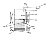
図1は本発明に係る結晶成長装置の構成例を示す図である。図1の例では、反応容器101内には、低融点かつ高蒸気圧の金属としてのNaと、少なくともIII族金属元素を含む物質としての金属Gaとが収容され、それらはIII族窒化物結晶が成長する温度領域で混合融液102を形成している。
【0033】
また、反応容器101内の空間領域には、少なくとも窒素元素を含む物質として窒素ガス(N2)103が充填されている。この窒素ガス103は、窒素供給管104を通して、反応容器101外から供給可能な状態となっており、窒素圧力を調整するために、図1の装置では、圧力調整機構105が設けられている。この圧力調整機構105は、例えば、圧力センサー及び圧力調整弁等により構成されており、この圧力調理機構105によって、反応容器101内の窒素圧力は、例えば50気圧に制御されている。
【0034】
また、反応容器101には、結晶成長可能な温度に制御可能な加熱装置106が具備されている。加熱装置106により反応容器101内をIII族窒化物結晶が成長する温度(例えば750℃)に制御することで、低融点かつ高蒸気圧の金属であるNaとIII族金属原料であるGaとの混合融液102が形成されるようになっている。このとき、混合融液102からIII族金属であるGaが供給され、加熱装置106によって反応容器101内を成長温度に一定保持することで、III族窒化物としてのGaN結晶が混合融液中107及び混合融液表面108で結晶成長するようになっている。
【0035】
このように、図1の結晶成長装置では、NaとGaの混合融液中107及び混合融液表面108で、窒素ガス或いは窒素ガスから供給された融液中の窒素成分とGaとが反応することで、継続的なGaN結晶が成長し、結晶サイズの大きなものを得ることが可能となる。
【0036】
また、図2は本発明に係る結晶成長装置の他の構成例を示す図である。なお、図2において、図1と同様の箇所には同じ符号を付している。
【0037】
図2の構成例では、反応容器101の外部にGaとNaの混合融液の融液ホルダー211があり、この融液ホルダー211はGaとNaの混合物が融液として存在できる温度に保持されている。この融液ホルダー211の上部の圧力供給管212から窒素ガスによって、反応容器101内の圧力より高い圧力を供給することで、融液ホルダー211に保持されているGaとNaの混合融液を、融液ホルダー供給管213を介して、反応容器101内部に供給可能になっている。
【0038】
このように、図2の構成例では、III族金属元素と他の元素とにより構成される混合物もしくは化合物を(例えば、GaとNaの混合融液を)、反応容器101の外部から供給可能となっている。ここで、反応容器101の外部より供給されるIII族金属元素と他の元素とにより構成される混合物もしくは化合物は、制御された量のみ反応容器101内に供給可能となっている。
【0039】
このように、GaとNaの混合融液を反応容器101の外部から供給することで、図1の説明で述べた継続的なGaN結晶の成長に加えて、Gaの反応容器101内での量を一定に保持することが可能となり、GaN結晶を一層安定して成長させることができる。
【0040】
なお、図2の例では、III族金属元素と他の元素とにより構成される混合物もしくは化合物を反応容器101の外部より供給するようにしているが、III族金属元素と他の元素とにより構成される混合物もしくは化合物を外部より供給するのではなく、図1に示したように、III族金属元素と他の元素とにより構成される混合物もしくは化合物を、反応容器101内に最初から存在させても良い。この場合、III族金属元素と他の元素とにより構成される混合物もしくは化合物であるGaとNaの混合融液が最初から反応容器101内に存在することで(III族金属元素と他の元素とにより構成される混合物もしくは化合物が、低融点かつ高蒸気圧の金属融液中に含まれていることで)、安定的に外乱が少なく結晶成長が継続し、結晶欠陥の少ないGaN結晶を成長することが可能となる。
【0041】
換言すれば、III族金属元素と他の元素とにより構成される混合物もしくは化合物が、III族窒化物結晶が成長する領域と空間的に分離した領域に存在していれば良い。
【0042】
図3は本発明に係る結晶成長装置の他の構成例を示す図である。なお、図3において、図1と同様の箇所には同じ符号を付している。
【0043】
図3の構成例が図1の構成例と異なるところは、図3の構成例では、反応容器101の加熱装置を、III族窒化物結晶が成長する領域を加熱する第一の加熱装置106と、III族金属元素と他の元素とにより構成される混合物もしくは化合物が存在する領域311を加熱する第二の加熱装置312とに分離している点である。
【0044】
図3の例では、III族金属元素と他の元素とにより構成される混合物もしくは化合物として、GaとNaの金属間化合物を用いており、その金属間化合物はIII族窒化物結晶が成長する領域から分離された領域311に存在している。この金属間化合物を加熱する第二の加熱装置312は、結晶成長する領域を加熱する第一の加熱装置106と分離していることで、独立的に温度制御が可能である。
【0045】
換言すれば、III族金属元素と他の元素とにより構成される混合物もしくは化合物が存在する領域の温度と、III族窒化物結晶が成長する領域の温度とを異なったものにすることができる。
【0046】
なお、上述の例では、第一の加熱装置106と第二の加熱装置312が分離制御する構造となっているが、加熱装置は必ずしも分離されている必要はなく、加熱装置が一つでIII族窒化物結晶を成長させる領域の温度と、III族元素と他の元素とにより構成される混合物若しくは化合物が存在する領域の温度とを相違させる構造となっていれば良い。
【0047】
具体的に、結晶成長領域を結晶成長温度として例えば750℃に第一の加熱装置106で加熱し、金属間化合物が存在する領域311を第二の加熱装置312で530℃に保持する。この状態では、領域311に存在する金属間化合物から徐々にIII族金属成分であるGaが、GaとNaの混合融液102中に溶出し、III族窒化物としてGaN結晶が混合融液中107および混合融液表面108で結晶成長する。ここで、GaとNaの金属間化合物からIII族金属成分であるGaが徐々に溶け出すことで、安定的に良質なIII族窒化物結晶を継続的に成長させることが可能となる。
【0048】
このように、図3の構成例では、III族金属元素と他の元素とにより構成される混合物もしくは化合物は、III族窒化物結晶が成長する領域107,108とは離れた領域311にあり、III族金属成分は、このIII族金属元素と他の元素とにより構成される混合物もしくは化合物が存在する領域311から、III族窒化物結晶が成長する領域107,108に供給される。このIII族窒化物結晶が成長する領域107,108に供給されたIII族金属成分と窒素元素を含む窒素成分とが反応することで、III族窒化物結晶を安定的に継続して成長させることができる。
【0049】
また、上述の例では、III族窒化物結晶を成長させる領域107,108の温度と、III族元素と他の元素とにより構成される混合物もしくは化合物が存在する領域311の温度とが異なっている場合について説明したが、本発明は、これら二つの領域の温度が異なっていなくても、空間的に二つの領域が分離されていれば良い。
【0050】
換言すれば、III族金属元素と他の元素とにより構成される混合物もしくは化合物が、III族窒化物結晶が成長する領域と空間的に分離した領域に存在していれば良い。
【0051】
図4は本発明に係る結晶成長装置の他の構成例を示す図である。図4の構成例では、反応容器401内には、低融点かつ高蒸気圧の金属としてNaがあり、NaはIII族窒化物結晶が成長する温度領域でNa融液402となっている。また、反応容器401の下部には、III族金属元素と他の元素とにより構成される混合物もしくは化合物として、例えばGaN409があり、GaN409はNa融液402で覆われている。
【0052】
また、反応容器401内の空間領域には、少なくとも窒素元素を含む物質として窒素ガス(N2)403が充填されている。この窒素ガス403は、窒素供給管404を通して、反応容器401の外部から供給可能となっている。この時、窒素圧力を調整するために、圧力調整機構405が設けられている。なお、この圧力調整機構405は圧力センサー及び圧力調整弁等から構成されている。この圧力調整機構405によって、反応容器401内の窒素圧力は、例えば50気圧に制御されている。
【0053】
また、反応容器401には、結晶成長可能な温度に制御できるように加熱装置406が具備されている。加熱装置406によりIII族窒化物結晶が成長する温度(例えば750℃)に反応容器401内を制御することで、低融点かつ高蒸気圧の金属であるNaが融液402となっており、このとき、GaN409は分解し、そこから徐々にGaが供給され、反応容器401内の温度を加熱装置406によって結晶成長温度に一定保持することで、III族窒化物としてのGaN結晶が混合融液中407および混合融液表面408で結晶成長する。
【0054】
ここで用いるGaN409は原料としてのものであり、単結晶のみならず、多結晶,非晶質でも良い。また、結晶性のものでも結晶欠陥が多いものや結晶サイズの小さいもの等のそのままでは基板として用いることが困難なものでも良い。従って、良質の基板として使用可能なサイズのGaN結晶を低コストで得ることが可能となる。
【0055】
このように、図4の構成例では、III族金属元素と他の元素とにより構成される混合物もしくは化合物を、III族窒化物結晶が成長する温度付近で分解あるいは溶融もしくは金属融液中に溶解させるようにしている。これにより、III族金属成分が、III族窒化物の結晶成長する領域に供給され、窒素成分と反応することで、III族窒化物結晶を成長させることができる。
【0056】
そして、本発明では、上述したような結晶成長方法,結晶成長装置により結晶成長させたIII族窒化物結晶を用いて、III族窒化物半導体デバイスを作製することができる。
【0057】
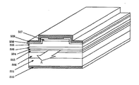
図5は本発明に係る半導体デバイスの構成例を示す図である。なお、図5の例では、半導体デバイスは半導体レーザとして構成されている。図5を参照すると、この半導体デバイスは、上述したような仕方で結晶成長させたIII族窒化物結晶(図5の例では、GaN結晶)を用いたn型GaN基板501上に、n型AlGaNクラッド層502、n型GaNガイド層503、InGaN MQW(多重量子井戸)活性層504、p型GaNガイド層505、p型AlGaNクラッド層506、p型GaNコンタクト層507が順次に結晶成長されている。この結晶成長方法としては、MO−VPE(有機金属気相成長)法やMBE(分子線エピタキシー)法等の薄膜結晶成長方法を用いることができる。
【0058】
次いで、GaN,AlGaN,InGaNの積層膜にリッジ構造を形成し、SiO2絶縁膜508をコンタクト領域のみ穴開けした状態で形成し、上部及び下部に各々p側オーミック電極Al/Ni 509及びn側オーミック電極Al/Ti 510を形成して、図5の半導体デバイス(半導体レーザ)が構成される。
【0059】
この半導体レーザのp側オーミック電極Al/Ni 509及びn側オーミック電極Al/Ti 510から電流を注入することで、この半導体レーザは発振し、図5の矢印Aの方向にレーザ光を出射させることができる。
【0060】
この半導体レーザは、本発明のIII族窒化物結晶(GaN結晶)を基板501として用いているため、半導体レーザデバイス中の結晶欠陥が少なく、大出力動作且つ長寿命のものとなっている。また、GaN基板501はn型であることから、基板501に直接電極510を形成することができ、第一の従来技術(第6図)のようにp側とn側の2つの電極を表面からのみ取り出すことが必要なく、低コスト化を図ることが可能となる。更に、光出射端面を劈開で形成することが可能となり、チップの分離と併せて、低コストで高品質なデバイスを実現することができる。
【0061】
なお、上述の各例では、低融点かつ高蒸気圧の金属としてアルカリ金属であるNaを用いているが、Naに限らず、K等を用いることもできる。すなわち、低融点かつ高蒸気圧の金属としては、III族窒化物結晶を成長させる温度において、融液となっているものであれば、Na以外のアルカリ金属を用いることもできる。
【0062】
また、上述の例では、少なくともIII族金属元素を含む物質として、Gaを用いているが、Gaに限らず、AlやIn等の単体の金属、あるいはそれらの混合物、合金等を用いることもできる。
【0063】
また、上述の例では、少なくとも窒素元素を含む物質として窒素ガスを用いているが、窒素ガスに限らず、NH3等のガスやNaN3等の固体を用いることもできる。
【0064】
また、上述の各例では、III族金属元素と他の元素とにより構成される混合物もしくは化合物として、GaNを用いたが、GaNに限らず、AlNやInN等の他のIII族窒化物を用いることもできる。
【0065】
また、III族金属元素と他の元素とにより構成される混合物もしくは化合物としては、GaNやAlN,InN等のIII族窒化物に限らず、例えばGaとNaの金属間化合物を用いて、III族窒化物として例えばGaNを結晶成長させても良い。この場合、GaとNaの金属間化合物は、GaNが結晶成長する温度(例えば750℃)付近では分解しており、III族金属成分としてのGaが結晶成長領域に供給可能である。また、III族金属元素と他の元素とにより構成される混合物もしくは化合物としては、上述したものに限らず、III族金属元素と他の元素とにより構成される合金であっても良い。
【0066】
具体的には、III族金属元素と他の元素から構成される混合物もしくは化合物として、GaとNaの金属間化合物,あるいはGaとKの金属間化合物を挙げることができる。また、他の合金として、GaとFeの合金、GaとCuの合金、GaとMnの合金、GaとCrの合金、GaとCoの合金を挙げることができる。例えばGaとFeの合金の場合には、成長温度が750〜850℃で分解することから、III族金属成分であるGaが結晶成長領域に供給可能となる。
【0067】
【発明の効果】
以上に説明したように、請求項1乃至請求項11記載の発明によれば、反応容器内で、低融点かつ高蒸気圧の金属融液中あるいは金属融液表面において、少なくともIII族金属元素を含む物質と少なくとも窒素元素を含む物質とから、III族金属元素と窒素元素とにより構成されるIII族窒化物を結晶成長させるようになっており、低融点かつ高蒸気圧の金属融液を用い、この金属融液中あるいは金属融液表面で結晶成長させることにより、高品質の結晶成長に必要かつ適切量のIII族金属成分を持続的に供給することが可能となる。その結果、低コストで結晶欠陥の少ない大型,高品質のIII族窒化物結晶の成長が実現できる(高品質で大型の結晶を育成するためには、適切量のIII族金属成分を結晶が成長する場に持続的に供給することが必要であり、結晶成長の場として金属融液を用いることで、このことが実現できる)。すなわち、前述した第1や第2の従来技術の問題点である工程を複雑化させることなく、第3の従来技術の問題点である高価な反応容器を用いることなく、かつ第3や第4の従来技術の問題点である結晶の大きさが小さくなることなく、高性能の発光ダイオードやLD等のデバイスを作製するための実用的な大きさのIII族窒化物結晶および半導体デバイスを提供することができる。
【0068】
特に、請求項2記載の発明では、請求項1記載の結晶成長方法において、低融点かつ高蒸気圧の金属融液中或いは金属融液表面に、III族金属元素と他の元素とにより構成される混合物もしくは化合物からIII族金属成分が供給されることで、請求項1の作用効果に加えて、徐々に安定的にIII族金属成分を結晶成長領域に供給でき、これにより、結晶欠陥が少なく、結晶品質の高いIII族窒化物結晶が実現できる。
【0069】
また、請求項3記載の発明では、III族金属元素と他の元素とにより構成される混合物もしくは化合物を、反応容器の外部より供給することで、請求項1,請求項2の作用効果に加えて、さらに、継続的なIII族金属成分の供給が可能となる。従って、より大面積のIII族窒化物結晶を高品質で継続的に成長させることが可能となる。
【0070】
また、請求項4記載の発明では、III族金属元素と他の元素とにより構成される混合物もしくは化合物が、低融点かつ高蒸気圧の金属融液中に含まれていることで、請求項1,請求項2の作用効果に加えて、結晶品質の高いIII族窒化物結晶の成長をスムーズに開始させることができる。その結果、結晶成長初期の種結晶の結晶品質が高く(結晶欠陥が少なく)、それを元に高品質のIII族窒化物結晶を成長させることが可能となる。
【0071】
また、請求項5記載の発明では、III族金属元素と他の元素とにより構成される混合物もしくは化合物が、III族窒化物結晶が成長する領域と空間的に分離した領域に存在することで、請求項1〜請求項4の作用効果に加えて、一層安定的にIII族金属成分を結晶成長領域に供給することができ、より結晶品質の高いIII族窒化物結晶を成長させることが可能となる。
【0072】
また、請求項6記載の発明では、III族金属元素と他の元素とにより構成される混合物もしくは化合物が存在する領域の温度と、III族窒化物結晶が成長する領域の温度とが異なっていることで、請求項5の作用効果に加えて、一層安定的にIII族金属成分を結晶成長領域に供給することができる。即ち、前述の混合物もしくは化合物が存在する領域から結晶成長領域にかけて、温度が変化していることから、III族金属成分は徐々に濃度が低くなり、継続的なIII族金属成分の拡散が可能となる。
【0073】
また、請求項7記載の発明では、III族金属元素と他の元素とにより構成される混合物もしくは化合物が、III族窒化物結晶が成長する温度付近で分解あるいは溶融もしくは金属融液中に溶解することで、請求項1〜請求項6の作用効果に加えて、III族金属成分を安定的に結晶成長領域に供給することができる。その結果、結晶品質の高いIII族窒化物結晶を成長させることが可能となる。
【0074】
また、請求項8記載の発明では、III族金属元素と他の元素とにより構成される混合物もしくは化合物が、III族金属元素と他の元素とにより構成される合金であることで、請求項1〜請求項7の作用効果に加えて、合金として存在している時には安定であり、より一層安定的にIII族金属成分をIII族窒化物結晶が成長する領域に供給可能となる。その結果、より一層結晶品質の高いIII族窒化物結晶を成長させることが可能となる。
【0075】
また、請求項9記載の発明では、低融点かつ高蒸気圧の金属がアルカリ金属であることで、請求項1〜請求項8の作用効果に加えて、アルカリ金属がより低融点であるために、低い温度でIII族窒化物結晶を成長させることが可能となる。
【0076】
また、請求項10記載の発明では、低融点かつ高蒸気圧の金属であるアルカリ金属がNaであることで、請求項9の作用効果に加えて、高純度かつ低コストで材料を入手することができ、更に取り扱いも比較的容易であり、安全性が高い。
【0077】
また、請求項12記載の発明によれば、請求項1乃至請求項10のいずれか一項に記載の結晶成長方法を用いてIII族窒化物結晶を結晶成長することで、半導体デバイスを作製することが可能な程度の大きく、かつ結晶品質の高いIII族窒化物結晶を、低コストで提供することが可能となる。
【0078】
また、請求項13記載の発明によれば、請求項12記載のIII族窒化物結晶を用いて半導体デバイスを作製することで、高性能なデバイスを低コストで実現できる。すなわち、このIII族窒化物結晶は、前述のように、結晶欠陥の少ない高品質な結晶であり、このIII族窒化物結晶を用いて、デバイスを作製し、あるいは、III族窒化物の薄膜結晶成長用の基板として用いて、薄膜成長からデバイス作製を行うことで、高性能なデバイスが実現できる。なお、ここで言う高性能とは、例えば半導体レーザや発光ダイオードの場合には、従来実現できていない高出力かつ長寿命なものであり、電子デバイスの場合には低消費電力,低雑音,高速動作,高温動作可能なものであり、受光デバイスとしては低雑音,長寿命等のものである。
【図面の簡単な説明】
【図1】本発明に係る結晶成長装置の構成例を示す図である。
【図2】本発明に係る結晶成長装置の他の構成例を示す図である。
【図3】本発明に係る結晶成長装置の他の構成例を示す図である。
【図4】本発明に係る結晶成長装置の他の構成例を示す図である。
【図5】本発明に係る半導体デバイスの構成例を示す図である。
【図6】従来のレーザダイオードを示す図である。
【符号の説明】
101 反応容器
102 混合融液
103 窒素ガス
104 窒素供給管
105 圧力調整機構
106 加熱装置(第一の加熱装置)
211 融液ホルダー
212 圧力供給管
213 融液ホルダー供給管
311 混合物もしくは化合物が存在する領域
312 第二の加熱装置
401 反応容器
402 融液
409 GaN
403 窒素ガス
404 窒素供給管
405 圧力調整機構
406 加熱装置
501 n型GaN基板
502 n型AlGaNクラッド層
503 n型GaNガイド層
504 InGaN MQW(多重量子井戸)活性層
505 p型GaNガイド層
506 p型AlGaNクラッド層
507 p型GaNコンタクト層
508 SiO2絶縁膜
509 p側オーミック電極Al/Ni
510 n側オーミック電極Al/Ti[0001]
BACKGROUND OF THE INVENTION
The present invention relates to a crystal growth method, a crystal growth apparatus, a group III nitride crystal, and a semiconductor device.
[0002]
[Prior art]
Currently, most of InGaAlN-based (Group III nitride) devices used as purple-blue-green light sources are MO-CVD (metal organic chemical vapor deposition) or MBE ( It is fabricated by crystal growth using a molecular beam crystal growth method) or the like. When sapphire or SiC is used as a substrate, crystal defects due to large difference in thermal expansion coefficient and difference in lattice constant from group III nitride increase. For this reason, there is a problem that the device characteristics are poor, for example, it is difficult to extend the life of the light emitting device, or the operating power is increased.
[0003]
Furthermore, in the case of a sapphire substrate, since it is insulative, it is impossible to take out the electrode from the substrate side as in the conventional light emitting device, and it is necessary to take out the electrode from the nitride semiconductor surface side where the crystal has grown. . As a result, there is a problem that the device area is increased, leading to high costs. In addition, a group III nitride semiconductor device fabricated on a sapphire substrate is difficult to be separated by cleaving, and it is not easy to cleave a resonator end face required for a laser diode (LD). For this reason, at present, resonator end faces are formed by dry etching, or resonator end faces are formed in a form close to cleavage after polishing the sapphire substrate to a thickness of 100 μm or less. Also in this case, it is impossible to easily separate the resonator end face and the chip as in a conventional LD in a single process, resulting in process complexity and cost.
[0004]
In order to solve this problem, it has been proposed to reduce crystal defects by performing selective lateral growth and other devices on a sapphire substrate for a group III nitride semiconductor film.
[0005]
For example, in the document “Japanese Journal of Applied Physics Vol. 36 (1997) Part 2, No. 12A, L1568-1571” (hereinafter referred to as the first prior art), a laser diode (LD) as shown in FIG. It is shown. In the laser diode of FIG. 6, the GaN low-temperature buffer layer 2 and the GaN layer 3 are sequentially grown on the sapphire substrate 1 by an MO-VPE (metal organic vapor phase epitaxy) apparatus, and then SiO 2 for selective growth.2A mask 4 is formed. This SiO2The mask 4 is formed by using another CVD (chemical vapor deposition) apparatus.2After the film is deposited, it is formed through a photolithography and etching process. Next, this SiO2A GaN film 3 ′ having a thickness of 20 μm is again grown on the mask 4 by the MO-VPE apparatus, so that GaN is selectively grown in the lateral direction and crystal defects are compared with the case where selective lateral growth is not performed. Is reduced. Further, by introducing a modulation-doped strained superlattice layer (MD-SLS) 5 formed thereon, crystal defects are prevented from extending to the active layer 6. As a result, the device lifetime can be increased as compared to the case where the selective lateral growth and modulation-doped strained superlattice layer is not used.
[0006]
In the case of this first prior art, it is possible to reduce crystal defects compared to the case where a GaN film is not selectively grown in the lateral direction on the sapphire substrate. The aforementioned problems with cleavage still remain. Furthermore, SiO2There is a new problem that the crystal growth by the MO-VPE apparatus is required twice with the mask formation process in between, and the process becomes complicated.
[0007]
As another method, for example, in the document “Applied Physics Letters, Vol. 73, No. 6, P832-834 (1998)” (hereinafter referred to as second prior art), a GaN thick film substrate is applied. It has been proposed. In the second prior art, after the selective lateral growth of 20 μm of the first prior art described above, a 200 μm thick GaN thick film is grown by an H-VPE (hydride vapor phase epitaxy) apparatus, and then this thickness is increased. The grown GaN film is polished from the sapphire substrate side to a thickness of 150 μm to produce a GaN substrate. Using the MO-VPE apparatus on this GaN substrate, crystal growth necessary for the LD device is sequentially performed to manufacture the LD device. As a result, in addition to the problem of crystal defects, it is possible to solve the above-described problems related to insulation and cleavage by using a sapphire substrate.
[0008]
However, the process of the second conventional technique is more complicated than that of the first conventional technique, which further increases the cost. Further, when a GaN thick film having a thickness of 200 μm is grown by the second prior art method, the stress accompanying the difference in lattice constant and thermal expansion coefficient from sapphire, which is the substrate, is increased, and the substrate is warped or cracked. A new problem arises.
[0009]
In order to avoid this problem, Japanese Patent Laid-Open No. 10-256661 proposes that the thickness of the original substrate (sapphire and spinel) on which the thick film is grown be 1 mm or more. In this way, by using a substrate having a thickness of 1 mm or more, even when a GaN film having a thickness of 200 μm is grown, the substrate is not warped or cracked. However, such a thick substrate has a high cost of the substrate itself and needs to spend a lot of time for polishing, leading to an increase in the cost of the polishing process. That is, when a thick substrate is used, the cost is higher than when a thin substrate is used. When a thick substrate is used, the substrate is not warped or cracked after the thick GaN film is grown, but stress is relaxed in the polishing process, and warping or cracking occurs during polishing. For this reason, even if a thick substrate is used, a GaN substrate having a high crystal quality cannot be easily produced with a large area.
[0010]
On the other hand, in the document “Journal of Crystal Growth, Vol.189 / 190, p.153-158 (1998)” (hereinafter referred to as third prior art), a bulk crystal of GaN is grown and homoepitaxially grown. It has been proposed to be used as a substrate. This technique is a technique for crystal growth of GaN from liquid Ga at a high temperature of 1400 to 1700 ° C. and a nitrogen pressure of several tens of kbar. In this case, a group III nitride semiconductor film necessary for the device can be grown using the bulk-grown GaN substrate. Therefore, a GaN substrate can be provided without complicating the process as in the first and second conventional techniques.
[0011]
However, in the third prior art, there is a problem that crystal growth at high temperature and high pressure is required, and a reaction vessel that can withstand the growth becomes extremely expensive. In addition, even with such a growth method, there is a problem that the size of the obtained crystal is at most about 1 cm, which is too small for practical use of the device.
[0012]
As a technique for solving this problem of GaN crystal growth under high temperature and high pressure, the document “Chemistry of Materials Vol.9 (1997) p.413-416” (hereinafter referred to as “fourth prior art”) includes: A GaN crystal growth method using Na as a flux has been proposed. This method uses sodium azide (NaN) as a flux.Three) And metal Ga as raw materials, sealed in a stainless steel reaction vessel (inner vessel dimensions; inner diameter = 7.5 mm, length = 100 mm) in a nitrogen atmosphere, and the reaction vessel is heated at a temperature of 600 to 800 ° C. for 24 to 24 ° C. By holding for 100 hours, a GaN crystal is grown. In the case of the fourth prior art, crystal growth at a relatively low temperature of about 600 to 800 ° C. is possible, and the pressure in the container is at most 100 kg / cm.2The point is that the pressure can be lowered compared with the third prior art. However, the problem with this method is that the crystal size obtained is small enough to be less than 1 mm. This size is too small for practical use of the device, as in the case of the third prior art.
[0013]
[Problems to be solved by the invention]
The present invention does not complicate the process that is the problem of the first and second prior arts, without using the expensive reaction vessel that is the problem of the third prior art, and the third and fourth. Providing practically sized Group III nitride crystals and semiconductor devices for fabricating high performance light emitting diodes, LDs, and other devices without reducing the size of crystals, which is a problem with conventional technologies Another object of the present invention is to provide a crystal growth method and a crystal growth apparatus capable of growing such a group III nitride crystal.
[0014]
[Means for Solving the Problems]
In order to achieve the above object, the invention according to claim 1 comprises a reaction vessel,alkaliIn metal melt oralkaliOn the surface of the metal meltA substance containing at least nitrogen element is supplied from outside during crystal growth,A group III nitride composed of a group III metal element and a nitrogen element is grown from a substance containing at least a group III metal element and a substance containing at least a nitrogen element.The group III metal component is supplied from a compound composed of a group III metal element and an alkali metal element or nitrogen element.It is characterized by that.
[0015]
The invention described in claim 2 is the crystal growth method according to claim 1,Anti-compoundIt is characterized by being supplied from the outside of the reaction container.
[0016]
Further, the invention according to claim 3 is the claim.1In the described crystal growth method,CompoundBut,Contained in alkali metal meltIt is characterized by that.
[0017]
Further, the invention described in claim 4 is the claim.Any one of claims 1 to 3In the described crystal growth method,Compound isIt exists in a region separated spatially from the region where the group III nitride crystal growsIt is characterized by that.
[0018]
Further, the invention according to claim 5 is the claim.4In the described crystal growth method,CompoundThe temperature of the existing region is different from the temperature of the region where the group III nitride crystal grows.It is characterized by that.
[0019]
Further, the invention described in claim 6 is the claim.Any one of claims 1 to 5In the described crystal growth method,Compound, Decomposition or melting near the temperature at which Group III nitride crystals grow, or dissolution in alkali metal meltsIt is characterized by that.
[0020]
The invention according to claim 7 is a1In the crystal growth method according to any one of claims 6 to 6.,Compound is Group IIIMetal elements and metalselementIs an alloy composed ofIt is characterized by that.
[0021]
The invention according to claim 8 is characterized in thatFrom 1The crystal growth method according to claim 7,The alkali metal is NaIt is characterized by that.
[0022]
The invention according to claim 9A step of holding a mixed melt containing a group III metal element and an alkali metal, a step of supplying a group III metal component from a compound composed of a group III metal element and an alkali metal element or nitrogen element, and crystal growth And supplying a substance containing nitrogen element from the outside to the mixed melt.It is characterized by that.
[0023]
Further, the invention described in claim 10 is described in claim 9.Method for producing group III nitride crystalInA step of growing a group III nitride crystal in the mixed melt or on the surface of the mixed melt;It is characterized by that.
[0024]
Further, the invention of claim 11 is a claim.9 or claim 10Described inThe method for producing a group III nitride crystal further includes a step of adjusting the pressure in the container holding the mixed melt.It is characterized by that.
[0025]
The invention according to claim 12 is the invention according to claims 9 to 9.11The method for producing a group III nitride crystal according to any one of the above, further includes a step of adjusting the temperature in the container holding the mixed melt.
[0026]
Further, the invention according to claim 13 is the claim.The method for producing a group III nitride crystal according to any one of claims 9 to 12, wherein the group III metal element is gallium and the alkali metal is sodium..
The invention according to claim 14 is the method for producing a group III nitride crystal according to any one of claims 9 to 13, wherein the substance containing nitrogen element is nitrogen gas. Yes.
[0027]
DETAILED DESCRIPTION OF THE INVENTION
Hereinafter, embodiments of the present invention will be described with reference to the drawings. The present invention provides a substance containing at least a group III metal element (for example, Ga (gallium)) and a substance containing at least a nitrogen element in a low melting point and high vapor pressure metal melt or on the surface of the metal melt in a reaction vessel. And crystal growth of a group III nitride composed of a group III metal element and a nitrogen element.
[0028]
More specifically, the temperature of the reaction vessel can be controlled so that the group III nitride can grow crystals. Further, the reaction vessel contains a metal having a low melting point and a high vapor pressure, and the metal having a low melting point and a high vapor pressure is a melt in a temperature region where the group III nitride can grow crystals. In this temperature-controlled reaction vessel, a metal having a low melting point and a high vapor pressure becomes a melt, and is composed of a group III metal element and a nitrogen element in the metal melt or on the surface of the metal melt. Group nitride crystals grow. Here, a substance containing at least a group III metal element and a substance containing at least a nitrogen element are raw materials for the group III nitride.
[0029]
Further, the present invention provides the above-described method for growing a group III nitride crystal, wherein a mixture composed of a group III metal element and other elements in a low melting point and high vapor pressure metal melt or on the surface of the metal melt or A group III metal component is supplied from the compound.
[0030]
Here, the group III metal component supplied from the mixture or compound composed of the group III metal element and other elements is at least nitrogen in the low melting point and high vapor pressure metal melt or on the surface of the metal melt. By reacting with a substance containing an element, a group III nitride crystal grows.
[0031]
In the following description, it is assumed that the metal having a low melting point and a high vapor pressure is Na, and the substance containing at least a group III metal element is metal Ga.
[0032]
FIG. 1 is a diagram showing a configuration example of a crystal growth apparatus according to the present invention. In the example of FIG. 1,
[0033]
Further, in the space region in the
[0034]
The
[0035]
As described above, in the crystal growth apparatus of FIG. 1, Ga reacts with the nitrogen component in the Na / Ga
[0036]
FIG. 2 is a diagram showing another configuration example of the crystal growth apparatus according to the present invention. In FIG. 2, the same parts as those in FIG.
[0037]
In the configuration example of FIG. 2, there is a
[0038]
As described above, in the configuration example of FIG. 2, a mixture or compound composed of a group III metal element and another element (for example, a mixed melt of Ga and Na) can be supplied from the outside of the
[0039]
Thus, by supplying a mixed melt of Ga and Na from the outside of the
[0040]
In the example of FIG. 2, a mixture or compound composed of a group III metal element and another element is supplied from the outside of the
[0041]
In other words, the mixture or compound composed of the Group III metal element and other elements may be present in a region spatially separated from the region where the Group III nitride crystal grows.
[0042]
FIG. 3 is a diagram showing another configuration example of the crystal growth apparatus according to the present invention. In FIG. 3, the same parts as those in FIG.
[0043]
The configuration example of FIG. 3 differs from the configuration example of FIG. 1 in that, in the configuration example of FIG. 3, the heating device of the
[0044]
In the example of FIG. 3, an intermetallic compound of Ga and Na is used as a mixture or compound composed of a group III metal element and another element, and the intermetallic compound is a region where a group III nitride crystal grows. It exists in the area |
[0045]
In other words, the temperature of the region where the mixture or compound composed of the group III metal element and other elements is present can be made different from the temperature of the region where the group III nitride crystal grows.
[0046]
In the above-described example, the
[0047]
Specifically, the crystal growth region is heated to, for example, 750 ° C. as the crystal growth temperature by the
[0048]
Thus, in the configuration example of FIG. 3, the mixture or compound composed of the group III metal element and the other elements is in the
[0049]
In the above example, the temperature of the
[0050]
In other words, the mixture or compound composed of the Group III metal element and other elements may be present in a region spatially separated from the region where the Group III nitride crystal grows.
[0051]
FIG. 4 is a diagram showing another configuration example of the crystal growth apparatus according to the present invention. In the configuration example of FIG. 4, there is Na as a low melting point and high vapor pressure metal in the
[0052]
Further, in the space region in the
[0053]
Further, the
[0054]
[0055]
Thus, in the configuration example of FIG. 4, a mixture or compound composed of a group III metal element and another element is decomposed or melted or dissolved in a metal melt near the temperature at which a group III nitride crystal grows. I try to let them. Thus, the group III metal component is supplied to the group III nitride crystal growth region and reacts with the nitrogen component, so that the group III nitride crystal can be grown.
[0056]
In the present invention, a group III nitride semiconductor device can be produced using a group III nitride crystal grown by the crystal growth method and the crystal growth apparatus as described above.
[0057]
FIG. 5 is a diagram showing a configuration example of a semiconductor device according to the present invention. In the example of FIG. 5, the semiconductor device is configured as a semiconductor laser. Referring to FIG. 5, this semiconductor device has an n-type AlGaN on an n-type GaN substrate 501 using a group III nitride crystal (GaN crystal in the example of FIG. 5) grown in the manner described above. A
[0058]
Next, a ridge structure is formed in the laminated film of GaN, AlGaN, and InGaN, and SiO 22The insulating
[0059]
By injecting current from the p-side ohmic electrode Al /
[0060]
Since this group III nitride crystal (GaN crystal) of the present invention is used as the substrate 501, this semiconductor laser has few crystal defects in the semiconductor laser device, has a large output operation and a long life. Further, since the GaN substrate 501 is n-type, the
[0061]
In each of the above examples, Na, which is an alkali metal, is used as a metal having a low melting point and a high vapor pressure. However, not only Na but also K or the like can be used. That is, as the metal having a low melting point and a high vapor pressure, an alkali metal other than Na can be used as long as it is a melt at the temperature at which the group III nitride crystal is grown.
[0062]
In the above example, Ga is used as the substance containing at least a group III metal element. However, not only Ga but a single metal such as Al or In, or a mixture or alloy thereof can be used. .
[0063]
Moreover, in the above-mentioned example, nitrogen gas is used as a substance containing at least nitrogen element.ThreeGas such as NaNThreeA solid such as can also be used.
[0064]
In each of the above examples, GaN is used as a mixture or compound composed of a group III metal element and another element. However, not only GaN but also other group III nitrides such as AlN and InN are used. You can also.
[0065]
Further, the mixture or compound composed of the Group III metal element and other elements is not limited to Group III nitrides such as GaN, AlN, and InN. For example, an intermetallic compound of Ga and Na is used to form Group III. For example, GaN may be grown as a nitride. In this case, the intermetallic compound of Ga and Na is decomposed near the temperature at which GaN grows (for example, 750 ° C.), and Ga as a group III metal component can be supplied to the crystal growth region. In addition, the mixture or compound composed of the group III metal element and other elements is not limited to the above-described one, but may be an alloy composed of the group III metal element and other elements.
[0066]
Specifically, examples of the mixture or compound composed of a Group III metal element and another element include an intermetallic compound of Ga and Na or an intermetallic compound of Ga and K. Other alloys include Ga and Fe alloys, Ga and Cu alloys, Ga and Mn alloys, Ga and Cr alloys, and Ga and Co alloys. For example, in the case of an alloy of Ga and Fe, since the growth temperature decomposes at 750 to 850 ° C., Ga which is a group III metal component can be supplied to the crystal growth region.
[0067]
【The invention's effect】
As described above, according to the invention described in claims 1 to 11, at least the group III metal element is present in the reaction vessel in the metal melt having a low melting point and high vapor pressure or on the surface of the metal melt. A group III nitride composed of a group III metal element and a nitrogen element is grown from a contained material and a substance containing at least a nitrogen element, and a low melting point and high vapor pressure metal melt is used. By growing crystals in the metal melt or on the surface of the metal melt, it is possible to continuously supply an appropriate amount of a group III metal component necessary for high-quality crystal growth. As a result, growth of large, high-quality group III nitride crystals with low crystal defects and low cost can be realized (in order to grow high-quality, large-scale crystals, crystals grow with an appropriate amount of group III metal components. It is necessary to supply continuously to the field to be used, and this can be realized by using a metal melt as a field for crystal growth). That is, without complicating the process which is the problem of the first and second prior arts described above, without using the expensive reaction vessel which is the problem of the third prior art, and the third and fourth. The present invention provides a III-nitride crystal and a semiconductor device having a practical size for manufacturing a device such as a high-performance light-emitting diode or LD without reducing the size of the crystal, which is a problem of the prior art. be able to.
[0068]
In particular, in the invention described in claim 2, in the crystal growth method described in claim 1, the crystal growth method is constituted by a group III metal element and other elements in the metal melt having a low melting point and a high vapor pressure or on the surface of the metal melt. In addition to the function and effect of Claim 1, the Group III metal component can be gradually and stably supplied to the crystal growth region by supplying the Group III metal component from the mixture or compound. A group III nitride crystal with high crystal quality can be realized.
[0069]
Further, in the invention according to claim 3, in addition to the effects of claims 1 and 2, the mixture or compound composed of the group III metal element and other elements is supplied from the outside of the reaction vessel. In addition, the Group III metal component can be continuously supplied. Therefore, it is possible to continuously grow a large group III nitride crystal with high quality.
[0070]
In the invention of claim 4, the mixture or compound composed of the group III metal element and other elements is contained in the metal melt having a low melting point and a high vapor pressure. In addition to the operation and effect of claim 2, the growth of a group III nitride crystal having high crystal quality can be started smoothly. As a result, the crystal quality of the seed crystal at the initial stage of crystal growth is high (there are few crystal defects), and it becomes possible to grow a high-quality group III nitride crystal based on the crystal quality.
[0071]
Further, in the invention of claim 5, the mixture or compound composed of the group III metal element and other elements is present in a region spatially separated from the region where the group III nitride crystal grows, In addition to the effects of the first to fourth aspects, the group III metal component can be more stably supplied to the crystal growth region, and a group III nitride crystal with higher crystal quality can be grown. Become.
[0072]
In the invention described in claim 6, the temperature of the region where the mixture or compound composed of the group III metal element and the other element is present is different from the temperature of the region where the group III nitride crystal grows. Thus, in addition to the function and effect of the fifth aspect, the group III metal component can be more stably supplied to the crystal growth region. That is, since the temperature changes from the region where the mixture or compound is present to the crystal growth region, the concentration of the Group III metal component gradually decreases, and the Group III metal component can be continuously diffused. Become.
[0073]
In the invention described in claim 7, the mixture or compound composed of the group III metal element and other elements is decomposed or melted or dissolved in the metal melt near the temperature at which the group III nitride crystal grows. Thus, in addition to the effects of the first to sixth aspects, the group III metal component can be stably supplied to the crystal growth region. As a result, a group III nitride crystal with high crystal quality can be grown.
[0074]
In the invention according to claim 8, the mixture or compound composed of the group III metal element and the other element is an alloy composed of the group III metal element and the other element. In addition to the effects of the seventh aspect, the alloy is stable when present as an alloy, and the group III metal component can be more stably supplied to the region where the group III nitride crystal grows. As a result, it is possible to grow a group III nitride crystal with higher crystal quality.
[0075]
Further, in the invention according to claim 9, since the metal having a low melting point and high vapor pressure is an alkali metal, in addition to the effects of claims 1 to 8, the alkali metal has a lower melting point. It becomes possible to grow a group III nitride crystal at a low temperature.
[0076]
In addition, in the invention described in claim 10, the alkali metal that is a metal having a low melting point and a high vapor pressure is Na. In addition, handling is relatively easy and safety is high.
[0077]
According to the invention described in claim 12, a semiconductor device is manufactured by growing a group III nitride crystal using the crystal growth method according to any one of claims 1-10. Therefore, it is possible to provide a group III nitride crystal having such a large size and high crystal quality as possible.
[0078]
According to the invention described in claim 13, a high-performance device can be realized at low cost by manufacturing a semiconductor device using the group III nitride crystal described in claim 12. That is, as described above, this group III nitride crystal is a high-quality crystal with few crystal defects, and a device is produced using this group III nitride crystal, or a group III nitride thin film crystal. A high-performance device can be realized by using a substrate for growth and manufacturing a device from a thin film growth. The high performance mentioned here means, for example, semiconductor lasers and light emitting diodes, which have not been realized in the past and have high output and long life, and in the case of electronic devices, low power consumption, low noise, and high speed. It can operate and operate at high temperature, and the light receiving device has low noise and long life.
[Brief description of the drawings]
FIG. 1 is a diagram showing a configuration example of a crystal growth apparatus according to the present invention.
FIG. 2 is a diagram showing another configuration example of the crystal growth apparatus according to the present invention.
FIG. 3 is a diagram showing another configuration example of the crystal growth apparatus according to the present invention.
FIG. 4 is a diagram showing another configuration example of the crystal growth apparatus according to the present invention.
FIG. 5 is a diagram showing a configuration example of a semiconductor device according to the present invention.
FIG. 6 is a diagram showing a conventional laser diode.
[Explanation of symbols]
101 reaction vessel
102 Mixed melt
103 nitrogen gas
104 Nitrogen supply pipe
105 Pressure adjustment mechanism
106 Heating device (first heating device)
211 Melt holder
212 Pressure supply pipe
213 Melt holder supply pipe
311 Regions where mixtures or compounds are present
312 Second heating device
401 reaction vessel
402 Melt
409 GaN
403 nitrogen gas
404 Nitrogen supply pipe
405 Pressure adjustment mechanism
406 Heating device
501 n-type GaN substrate
502 n-type AlGaN cladding layer
503 n-type GaN guide layer
504 InGaN MQW (Multiple Quantum Well) Active Layer
505 p-type GaN guide layer
506 p-type AlGaN cladding layer
507 p-type GaN contact layer
508 SiO2Insulation film
509 p-side ohmic electrode Al / Ni
510 n-side ohmic electrode Al / Ti
Claims (14)
III族金属成分がIII族金属元素とアルカリ金属元素または窒素元素とにより構成される化合物から供給される工程と、
結晶成長中、窒素元素を含む物質を外部から前記混合融液に供給する工程とを備えるIII族窒化物結晶の製造方法。Holding a mixed melt containing a Group III metal element and an alkali metal;
A step of supplying a Group III metal component from a compound composed of a Group III metal element and an alkali metal element or a nitrogen element;
And a step of supplying a substance containing nitrogen element to the mixed melt from outside during crystal growth.
前記アルカリ金属は、ナトリウムである、請求項9から請求項12のいずれか1項に記載のIII族窒化物結晶の製造方法。The group III metal element is gallium,
The method for producing a group III nitride crystal according to any one of claims 9 to 12, wherein the alkali metal is sodium.
Priority Applications (7)
| Application Number | Priority Date | Filing Date | Title |
|---|---|---|---|
| JP27704599A JP3929657B2 (en) | 1999-09-29 | 1999-09-29 | Crystal growth method and group III nitride crystal production method |
| US09/590,063 US6592663B1 (en) | 1999-06-09 | 2000-06-08 | Production of a GaN bulk crystal substrate and a semiconductor device formed on a GaN bulk crystal substrate |
| US10/601,301 US7250640B2 (en) | 1999-06-09 | 2003-06-13 | Production of a GaN bulk crystal substrate and a semiconductor device formed on a GaN bulk crystal substrate |
| US11/408,656 US7508003B2 (en) | 1999-06-09 | 2006-04-20 | Production of a GaN bulk crystal substrate and a semiconductor device formed thereon |
| US12/367,013 US8591647B2 (en) | 1999-06-09 | 2009-02-06 | Production of a GaN bulk crystal substrate and a semiconductor device formed thereon |
| US14/057,690 US20140044970A1 (en) | 1999-06-09 | 2013-10-18 | PRODUCTION OF A GaN BULK CRYSTAL SUBSTRATE AND A SEMICONDUCTOR DEVICE FORMED ON A GaN BULK CRYSTAL SUBSTRATE |
| US14/619,237 US9869033B2 (en) | 1999-06-09 | 2015-02-11 | Production of a GaN bulk crystal substrate and a semiconductor device formed on a GaN bulk crystal substrate |
Applications Claiming Priority (1)
| Application Number | Priority Date | Filing Date | Title |
|---|---|---|---|
| JP27704599A JP3929657B2 (en) | 1999-09-29 | 1999-09-29 | Crystal growth method and group III nitride crystal production method |
Related Child Applications (1)
| Application Number | Title | Priority Date | Filing Date |
|---|---|---|---|
| JP2006172448A Division JP2007001858A (en) | 2006-06-22 | 2006-06-22 | Crystal manufacturing apparatus, group iii nitride crystal and semiconductor device |
Publications (3)
| Publication Number | Publication Date |
|---|---|
| JP2001102316A JP2001102316A (en) | 2001-04-13 |
| JP2001102316A5 JP2001102316A5 (en) | 2006-03-30 |
| JP3929657B2 true JP3929657B2 (en) | 2007-06-13 |
Family
ID=17578026
Family Applications (1)
| Application Number | Title | Priority Date | Filing Date |
|---|---|---|---|
| JP27704599A Expired - Lifetime JP3929657B2 (en) | 1999-06-09 | 1999-09-29 | Crystal growth method and group III nitride crystal production method |
Country Status (1)
| Country | Link |
|---|---|
| JP (1) | JP3929657B2 (en) |
Cited By (1)
| Publication number | Priority date | Publication date | Assignee | Title |
|---|---|---|---|---|
| CN104962995A (en) * | 2015-07-23 | 2015-10-07 | 北京大学东莞光电研究院 | Device and method for growing nitride monocrystal |
Families Citing this family (26)
| Publication number | Priority date | Publication date | Assignee | Title |
|---|---|---|---|---|
| JP2002319545A (en) * | 2001-04-20 | 2002-10-31 | Mitsubishi Cable Ind Ltd | MANUFACTURING METHOD OF GaN CRYSTAL AND BASE MATERIAL FOR CRYSTAL GROWTH |
| JP4640899B2 (en) * | 2001-06-28 | 2011-03-02 | 株式会社リコー | Group III nitride crystal growth equipment |
| US7001457B2 (en) | 2001-05-01 | 2006-02-21 | Ricoh Company, Ltd. | Crystal growth method, crystal growth apparatus, group-III nitride crystal and group-III nitride semiconductor device |
| US6949140B2 (en) | 2001-12-05 | 2005-09-27 | Ricoh Company, Ltd. | Crystal growth method, crystal growth apparatus, group-III nitride crystal and group-III nitride semiconductor device |
| US7220311B2 (en) | 2002-11-08 | 2007-05-22 | Ricoh Company, Ltd. | Group III nitride crystal, crystal growth process and crystal growth apparatus of group III nitride |
| US7261775B2 (en) | 2003-01-29 | 2007-08-28 | Ricoh Company, Ltd. | Methods of growing a group III nitride crystal |
| JP5229103B2 (en) * | 2003-03-25 | 2013-07-03 | 株式会社リコー | Group III nitride crystal manufacturing method |
| JP4457576B2 (en) * | 2003-05-08 | 2010-04-28 | 住友電気工業株式会社 | Group III-V compound crystal and method for producing the same |
| JP5212332B2 (en) * | 2003-10-31 | 2013-06-19 | 住友電気工業株式会社 | Method for producing group III nitride crystal |
| JP4534631B2 (en) | 2003-10-31 | 2010-09-01 | 住友電気工業株式会社 | Method for producing group III nitride crystal |
| US20070196942A1 (en) * | 2003-12-26 | 2007-08-23 | Yusuke Mori | Method for producing group III nitride crystal, group III nitride crystal obtained by such method, and group III nitride substrate using the same |
| JP2005194146A (en) * | 2004-01-08 | 2005-07-21 | Sumitomo Electric Ind Ltd | Production method for group iii nitride crystal |
| WO2005085503A1 (en) * | 2004-03-09 | 2005-09-15 | Dai Nippon Printing Co., Ltd. | Method for producing corundam crystal |
| JP2005263511A (en) * | 2004-03-16 | 2005-09-29 | Ricoh Co Ltd | Crystal growth method of group iii nitride, group iii nitride crystal and semiconductor device |
| WO2005095681A1 (en) * | 2004-03-31 | 2005-10-13 | Matsushita Electric Industrial Co., Ltd. | Method for producing iii group element nitride crystal, production apparatus for use therein, and semiconductor element produced thereby |
| EP1741807B1 (en) | 2004-04-27 | 2013-09-25 | Panasonic Corporation | Apparatus for production of crystal of group iii element nitride and process for producing crystal of group iii element nitride |
| EP1754810B1 (en) | 2004-05-19 | 2011-05-18 | Sumitomo Electric Industries, Ltd. | Method for producing group iii nitride semiconductor crystal |
| WO2006003955A1 (en) * | 2004-06-30 | 2006-01-12 | Matsushita Electric Industrial Co., Ltd. | Acousto-optical element and optical drawing device using same |
| JP4603498B2 (en) | 2005-03-14 | 2010-12-22 | 株式会社リコー | Group III nitride crystal manufacturing method and manufacturing apparatus |
| CN101175875B (en) | 2005-05-12 | 2010-12-15 | 株式会社理光 | Method and apparatus for producing group III element nitride crystal, and group iii element nitride crystal |
| JP4856934B2 (en) | 2005-11-21 | 2012-01-18 | 株式会社リコー | GaN crystal |
| CN101370971A (en) * | 2006-02-13 | 2009-02-18 | 日本碍子株式会社 | Method of recovering sodium metal from flux |
| US20070215034A1 (en) | 2006-03-14 | 2007-09-20 | Hirokazu Iwata | Crystal preparing device, crystal preparing method, and crystal |
| KR101192061B1 (en) | 2006-11-14 | 2012-10-17 | 고꾸리쯔 다이가꾸 호우징 오사까 다이가꾸 | GaN CRYSTAL PRODUCING METHOD, GaN CRYSTAL, GaN CRYSTAL SUBSTRATE, SEMICONDUCTOR DEVICE AND GaN CRYSTAL PRODUCING APPARATUS |
| US7708833B2 (en) | 2007-03-13 | 2010-05-04 | Toyoda Gosei Co., Ltd. | Crystal growing apparatus |
| JP4956515B2 (en) * | 2008-09-26 | 2012-06-20 | 株式会社リコー | Method for producing group III nitride crystal |
-
1999
- 1999-09-29 JP JP27704599A patent/JP3929657B2/en not_active Expired - Lifetime
Cited By (2)
| Publication number | Priority date | Publication date | Assignee | Title |
|---|---|---|---|---|
| CN104962995A (en) * | 2015-07-23 | 2015-10-07 | 北京大学东莞光电研究院 | Device and method for growing nitride monocrystal |
| CN104962995B (en) * | 2015-07-23 | 2017-07-28 | 北京大学东莞光电研究院 | The grower and method of a kind of nitride single-crystal |
Also Published As
| Publication number | Publication date |
|---|---|
| JP2001102316A (en) | 2001-04-13 |
Similar Documents
| Publication | Publication Date | Title |
|---|---|---|
| JP3929657B2 (en) | Crystal growth method and group III nitride crystal production method | |
| JP4801315B2 (en) | Method for producing group III nitride crystal | |
| JP4011828B2 (en) | Method for crystal growth of group III nitride crystal and method for manufacturing group III nitride crystal | |
| JP4055110B2 (en) | Method for producing group III nitride crystal | |
| JP4245822B2 (en) | Method for producing group III nitride crystal | |
| JP4216612B2 (en) | Method for producing group III nitride crystal | |
| JP3966682B2 (en) | Crystal growth method, crystal growth apparatus, crystal production apparatus, and crystal production method | |
| JP3868156B2 (en) | Crystal growth method, crystal growth apparatus and group III nitride crystal | |
| JP4560307B2 (en) | Group III nitride crystal manufacturing method | |
| JP4056664B2 (en) | Method for producing group III nitride crystal | |
| JP2003238296A (en) | Method and apparatus for growing group iii nitride crystal | |
| JP4640899B2 (en) | Group III nitride crystal growth equipment | |
| JP4048476B2 (en) | III-nitride crystal manufacturing apparatus with observation function and nitride crystal manufacturing method | |
| JP4551026B2 (en) | Group III nitride crystal growth apparatus and group III nitride crystal growth method | |
| JP4298153B2 (en) | Method for producing group III nitride crystal | |
| JP2007001858A (en) | Crystal manufacturing apparatus, group iii nitride crystal and semiconductor device | |
| JP2003160398A (en) | Method and apparatus for growth of group iii nitride crystal | |
| JP4971274B2 (en) | Method for producing group III nitride crystal | |
| JP4956515B2 (en) | Method for producing group III nitride crystal | |
| JP4414247B2 (en) | Group III nitride crystal manufacturing method | |
| JP5113097B2 (en) | Group III nitride crystal manufacturing method | |
| JP4773408B2 (en) | Group III nitride crystal production method and crystal growth apparatus | |
| JP4768656B2 (en) | Crystal growth equipment | |
| JP5971297B2 (en) | Crystal manufacturing equipment | |
| JP5278456B2 (en) | Method for producing group III nitride crystal |
Legal Events
| Date | Code | Title | Description |
|---|---|---|---|
| RD02 | Notification of acceptance of power of attorney |
Free format text: JAPANESE INTERMEDIATE CODE: A7422 Effective date: 20060201 |
|
| A521 | Written amendment |
Free format text: JAPANESE INTERMEDIATE CODE: A523 Effective date: 20060208 |
|
| RD04 | Notification of resignation of power of attorney |
Free format text: JAPANESE INTERMEDIATE CODE: A7424 Effective date: 20060210 |
|
| A131 | Notification of reasons for refusal |
Free format text: JAPANESE INTERMEDIATE CODE: A131 Effective date: 20060228 |
|
| A521 | Written amendment |
Free format text: JAPANESE INTERMEDIATE CODE: A523 Effective date: 20060403 |
|
| A02 | Decision of refusal |
Free format text: JAPANESE INTERMEDIATE CODE: A02 Effective date: 20060509 |
|
| A521 | Written amendment |
Free format text: JAPANESE INTERMEDIATE CODE: A523 Effective date: 20060620 |
|
| A521 | Written amendment |
Free format text: JAPANESE INTERMEDIATE CODE: A523 Effective date: 20060621 |
|
| A521 | Written amendment |
Free format text: JAPANESE INTERMEDIATE CODE: A821 Effective date: 20060607 |
|
| A911 | Transfer to examiner for re-examination before appeal (zenchi) |
Free format text: JAPANESE INTERMEDIATE CODE: A911 Effective date: 20061023 |
|
| A131 | Notification of reasons for refusal |
Free format text: JAPANESE INTERMEDIATE CODE: A131 Effective date: 20070116 |
|
| A521 | Written amendment |
Free format text: JAPANESE INTERMEDIATE CODE: A523 Effective date: 20070131 |
|
| A521 | Written amendment |
Free format text: JAPANESE INTERMEDIATE CODE: A523 Effective date: 20070220 |
|
| TRDD | Decision of grant or rejection written | ||
| A01 | Written decision to grant a patent or to grant a registration (utility model) |
Free format text: JAPANESE INTERMEDIATE CODE: A01 Effective date: 20070306 |
|
| A61 | First payment of annual fees (during grant procedure) |
Free format text: JAPANESE INTERMEDIATE CODE: A61 Effective date: 20070307 |
|
| R150 | Certificate of patent or registration of utility model |
Free format text: JAPANESE INTERMEDIATE CODE: R150 Ref document number: 3929657 Country of ref document: JP Free format text: JAPANESE INTERMEDIATE CODE: R150 |
|
| FPAY | Renewal fee payment (event date is renewal date of database) |
Free format text: PAYMENT UNTIL: 20110316 Year of fee payment: 4 |
|
| R250 | Receipt of annual fees |
Free format text: JAPANESE INTERMEDIATE CODE: R250 |
|
| FPAY | Renewal fee payment (event date is renewal date of database) |
Free format text: PAYMENT UNTIL: 20120316 Year of fee payment: 5 |
|
| R250 | Receipt of annual fees |
Free format text: JAPANESE INTERMEDIATE CODE: R250 |
|
| FPAY | Renewal fee payment (event date is renewal date of database) |
Free format text: PAYMENT UNTIL: 20130316 Year of fee payment: 6 |
|
| FPAY | Renewal fee payment (event date is renewal date of database) |
Free format text: PAYMENT UNTIL: 20140316 Year of fee payment: 7 |
|
| R250 | Receipt of annual fees |
Free format text: JAPANESE INTERMEDIATE CODE: R250 |
|
| EXPY | Cancellation because of completion of term |