JP4456606B2 - Method, computer program, and system for performing power routing on a voltage island in an integrated circuit chip - Google Patents
Method, computer program, and system for performing power routing on a voltage island in an integrated circuit chip Download PDFInfo
- Publication number
- JP4456606B2 JP4456606B2 JP2006534426A JP2006534426A JP4456606B2 JP 4456606 B2 JP4456606 B2 JP 4456606B2 JP 2006534426 A JP2006534426 A JP 2006534426A JP 2006534426 A JP2006534426 A JP 2006534426A JP 4456606 B2 JP4456606 B2 JP 4456606B2
- Authority
- JP
- Japan
- Prior art keywords
- power
- robust
- generating
- determining
- program code
- Prior art date
- Legal status (The legal status is an assumption and is not a legal conclusion. Google has not performed a legal analysis and makes no representation as to the accuracy of the status listed.)
- Expired - Fee Related
Links
Images


Classifications
-
- H—ELECTRICITY
- H01—ELECTRIC ELEMENTS
- H01L—SEMICONDUCTOR DEVICES NOT COVERED BY CLASS H10
- H01L23/00—Details of semiconductor or other solid state devices
- H01L23/52—Arrangements for conducting electric current within the device in operation from one component to another, i.e. interconnections, e.g. wires, lead frames
-
- G—PHYSICS
- G06—COMPUTING; CALCULATING OR COUNTING
- G06F—ELECTRIC DIGITAL DATA PROCESSING
- G06F30/00—Computer-aided design [CAD]
- G06F30/30—Circuit design
- G06F30/39—Circuit design at the physical level
- G06F30/394—Routing
-
- H—ELECTRICITY
- H01—ELECTRIC ELEMENTS
- H01L—SEMICONDUCTOR DEVICES NOT COVERED BY CLASS H10
- H01L23/00—Details of semiconductor or other solid state devices
- H01L23/52—Arrangements for conducting electric current within the device in operation from one component to another, i.e. interconnections, e.g. wires, lead frames
- H01L23/522—Arrangements for conducting electric current within the device in operation from one component to another, i.e. interconnections, e.g. wires, lead frames including external interconnections consisting of a multilayer structure of conductive and insulating layers inseparably formed on the semiconductor body
- H01L23/528—Geometry or layout of the interconnection structure
- H01L23/5286—Arrangements of power or ground buses
-
- H—ELECTRICITY
- H01—ELECTRIC ELEMENTS
- H01L—SEMICONDUCTOR DEVICES NOT COVERED BY CLASS H10
- H01L2924/00—Indexing scheme for arrangements or methods for connecting or disconnecting semiconductor or solid-state bodies as covered by H01L24/00
- H01L2924/0001—Technical content checked by a classifier
- H01L2924/0002—Not covered by any one of groups H01L24/00, H01L24/00 and H01L2224/00
Landscapes
- Engineering & Computer Science (AREA)
- Physics & Mathematics (AREA)
- Computer Hardware Design (AREA)
- General Physics & Mathematics (AREA)
- Geometry (AREA)
- Theoretical Computer Science (AREA)
- Microelectronics & Electronic Packaging (AREA)
- Power Engineering (AREA)
- Condensed Matter Physics & Semiconductors (AREA)
- Computer Networks & Wireless Communication (AREA)
- Evolutionary Computation (AREA)
- General Engineering & Computer Science (AREA)
- Semiconductor Integrated Circuits (AREA)
- Design And Manufacture Of Integrated Circuits (AREA)
Description
本発明は、一般に集積回路設計、特にボルテージアイランド(voltage island)を有する集積回路で電力を割り当てるための方法および装置に関する。さら詳しくは、本発明は、集積回路チップ内のボルテージアイランド上で電力ルーティング(power routing)を行なうための方法および装置に関する。 The present invention relates generally to integrated circuit designs, and more particularly to a method and apparatus for allocating power in an integrated circuit having a voltage island. More particularly, the present invention relates to a method and apparatus for performing power routing on a voltage island in an integrated circuit chip.
ボルテージアイランドの概念は、性能の増加およびより電力消費の低下に伴って、同じ集積回路チップ上に多数の設計技術を集積するために、集積回路設計へ導入されている。ボルテージアイランドの概念は、集積回路チップの1つ以上の部分(アイランド)がチップワイド電源(VDDg)および他のボルテージアイランド電源(VDDi−VDDn)の両方によって電力供給されることを可能にし,VDDgとVDDi−VDDnは、集積回路の操作上の要求に従って断続的に切り替えることができる。典型的には、VDDgおよびVDDi−VDDn(GNDと同様に)は、別個のチップワイド電源からボルテージアイランドに供給される。 The concept of voltage islands has been introduced into integrated circuit designs to integrate multiple design technologies on the same integrated circuit chip with increased performance and lower power consumption. The concept of voltage island allows one or more portions (islands) of an integrated circuit chip to be powered by both chip-wide power supply (VDDg) and other voltage island power supplies (VDDi-VDDn), VDDg and VDDi-VDDn can be switched intermittently according to the operational requirements of the integrated circuit. Typically, VDDg and VDDi-VDDn (similar to GND) are supplied to the voltage island from separate chip-wide power supplies.
一般的に、ボルテージアイランドは、チップ電力網(chip power grid)の残りの部分から分離された電源供給網構造(isolated power supply grid structure)を必要とする。従って、電磁気的またはIRドロップ違反(IR drop violation)のないボルテージアイランドのための電気的ロバスト(electrically robust)電力網構造を生成するために、オフチップおよびオンチップ電源は、ルートを決める必要がある。典型的には、ボルテージアイランドのためのオフチップ電源は、C4ボールグリッドアレイ位置、またはワイヤボンドの位置のいずれかから始まり、ボルテージアイランドのためのオンチップ電源は、電圧調整マクロピンで始まる。 In general, voltage islands require an isolated power supply grid structure that is separate from the rest of the chip power grid. Thus, off-chip and on-chip power supplies need to be routed to generate an electrically robust power network structure for voltage islands without electromagnetic or IR drop violations. Typically, the off-chip power supply for the voltage island starts at either the C4 ball grid array location or the wire bond location, and the on-chip power supply for the voltage island starts with a voltage regulation macro pin.
VDDg、VDDi−VDDnおよびGNDからボルテージアイランドに対して効率的な電力接続を有するために、多くの問題を克服する必要がある。克服される必要がある問題としては、等外のボルテージアイランドの電力必要性を予想する電力線の過剰を必要としない方法、局部的に希薄な電力網のために、ボルテージアイランド回路内に含まれる電力提供端末の配置を制限しない方法、エレクトロマイグレーション(electromigration)およびIRドロップ違反を避ける方法およびピンのブロックや他のワイヤアビリティ(wireability)の問題を回避する方法が挙げられる。 In order to have an efficient power connection from VDDg, VDDi-VDDn and GND to the voltage island, many problems need to be overcome. Problems that need to be overcome include providing power contained within the voltage island circuit for methods that do not require excessive power lines to anticipate the power needs of extraordinary voltage islands, locally sparse power networks, etc. Methods that do not limit terminal placement, methods that avoid electromigration and IR drop violations, and methods that avoid pin blocking and other wireability problems.
本開示は、集積回路チップ内のボルテージアイランド上に電力ルーティングを行なうための改良方法を提供する。 The present disclosure provides an improved method for performing power routing on voltage islands in an integrated circuit chip.
本発明の好ましい実施例によって、第1の電力網は、金属レベル1からN−1においてボルテージアイランドのために生成される。次いで、第2の電力網は、金属レベルN以上において生成される。第2のロバスト電力網の境界領域が決まる。最後に、1セットの電源からの最短距離接続は、第2の電力網に対してルートが決められる。 According to a preferred embodiment of the present invention, a first power grid is generated for voltage islands at metal levels 1 to N-1. A second power grid is then generated above the metal level N. A boundary region of the second robust power network is determined. Finally, the shortest distance connection from a set of power supplies is routed to the second power grid.
本発明の目的、特徴および利点は、すべて次の詳細な説明において明白になるであろう。 All objects, features and advantages of the present invention will become apparent in the following detailed description.
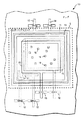
図面、特に図1を参照すると、本発明の好ましい実施例を実施することができるボルテージアイランドを有する集積回路チップの図が示されている。図示するように、集積回路チップ10は、ボルテージアイランド5を含む。ボルテージアイランド5は、チップVDDg電力網12から供給されるVDDg電力ネットワーク11、チップGND電力網14から供給されるGND電力ネットワーク13、オンチップVDDi−VDDn電力網16から供給されるVDDi−VDDn電力ネットワーク15、および(任意に)オンチップGNDi−GNDn電力網18から供給されるGNDi−GNDn電力ネットワーク17を含む。ボルテージアイランド5は、また、ボルテージアイランド5に含まれる回路および装置に電力を供給するための電力提供端末(PST)19を含む。PST19は、VDDg、VDDi−VDDnおよびGNDに接続されなければならない。
Referring to the drawings, and in particular to FIG. 1, there is shown a diagram of an integrated circuit chip having a voltage island in which the preferred embodiment of the present invention can be implemented. As illustrated, the
VDDg電力ネットワーク11、GND電力ネットワーク13およびVDDi−VDDn電力ネットワーク15は、図1で電力環(power ring)として示されるが、グリッドなどの他のタイプの構成も同様に可能であることは当業者によって理解される。
Although the
図2を参照すると、本発明の好ましい実施例よる図1の集積回路チップ10の断面図が示されている。図示するように、ボルテージアイランド5のための電力網は、2つのグループ、すなわち、金属レベル1から金属レベルN−1に位置する第1の電力網21および金属レベルN以上に位置する第2の電力網22に分割されるのが好ましい。または、第2の電力網22は、電力セグメントの形態とすることができる。電力セグメントは、わずか1レベルの金属ラインを有する電力網として定義される。第2の電力網22のための適切な入力および必須条件は、次のとおりである。
1.電力網ソースポイント(ボールグリッドアレイパッド、電圧調整ピン、図2に示すワイヤボンドパッド23のいずれかまたはその組み合わせ)。
2.特定の金属レベルまで電力網を要求する、定義されたサイズのボルテージアイランド。
Referring to FIG. 2, there is shown a cross-sectional view of the
1. Power grid source point (ball grid array pad, voltage adjustment pin,
2. A voltage island of defined size that requires a power grid to a specific metal level.
図3を参照すると、本発明の好ましい実施例による集積回路チップ内のボルテージアイランド上で電力ルーティングを行なう方法の上位論理流れ図が示されている。ブロック30でスタートして、ブロック31で示されるように、ボルテージアイランドのための第1の電力網は、金属レベル1から金属レベルN−1において生成される。前記ロバスト電力網生成は、チップ電力網生成に類似する技術を使用して行なわれるのが好ましい。次いで、ボルテージアイランドのための第2の電力網は、ブロック32で示されるように、金属レベルN以上において生成される。上述されるように、前記第2の電力網は、電力セグメント(すなわち、金属層をひとつのみ有する)の形態とすることができる。金属レベルN以上においてルートが決められる電力セグメントの数(S)は、電源の数と電源ごとになされる接続数の積によって決まるのが好ましい。電源は、それぞれ単一の広いワイヤーではなく多数のワイヤーを使用して、ボルテージアイランドに接続されていてもよい。多数のワイヤーの幅は、電気的な制約のすべてを満足するために調節することができる。
Referring to FIG. 3, there is shown a high-level logic flow diagram of a method for performing power routing on voltage islands in an integrated circuit chip according to a preferred embodiment of the present invention. Starting at
次に、ブロック33で示されるように、前記第2の電力網の境界領域が決まる。前記第2の電力網が電力セグメントから形成される場合、すべての電力セグメント(S)は、すべてロバスト第2の電力網が境界領域を横断して形成され、該境界領域の全長を拡張することができるように、金属レベルNにおいてルートが決められる。続いて、ブロック34で示されるように、1セットの最短距離接続は、様々な電源から前記第2の電力網(または、金属層Nにおけるそれぞれの電力セグメントに)へのルートが決められる。前記ルータは、各接続のためにスタート/エンドシェイプでエントリを有する配列を構築する。そのような配列は、ルータが金属レベルNにおいて、電源から特定の電源セグメントに最短距離接続を保証できるように、距離によって分類される。
Next, as indicated by
図3のブロック32内のステップは、さらに、以下のように拡張することができる。
1.チップ上で電源シェイプ(同じ電圧極性の)の数値総数を得る。
2.ボルテージアイランドが位置するチップ位置を識別する。
3.ルーティングが行なわれるボルテージアイランド上面に境界領域を計算して生成する。
4.境界領域内に電力網を生成する。
The steps in
1. Get the total number of power shapes (of the same voltage polarity) on the chip.
2. The chip position where the voltage island is located is identified.
3. A boundary region is calculated and generated on the upper surface of the voltage island where routing is performed.
4). A power grid is generated in the boundary region.
図3のブロック33のステップは、さらに、電源を備えたキーワードの関連付けを含み、ボルテージアイランドは、どの電源を複合ボルテージアイランド・インスタンス・シナリオ下で、ボルテージアイランド上面に電力網の正確なセットに接続しなければならないかを識別する。
The step of
図3のブロック34のステップは、さらに、以下のように展開することができる。
for eachvoltage VDDi, do {
get source points into agroup known as group_A;
dividegroup_A based on the connection per source information;
get thetarget power shapes (the second robust power grid on metal level N and above)to build a group_B;
for a givenshape s in group_A, do {
call ShapeRouter to routefrom s to t in group_B
}
}
The steps of
for eachvoltage VDD i , do {
get source points into agroup known as group_A;
dividegroup_A based on the connection per source information;
get thetarget power shapes (the second robust power grid on metal level N and above) to build a group_B;
for a givenshape s in group_A, do {
call ShapeRouter to routefrom s to t in group_B
}
}
図4を参照すると、本発明の好ましい実施例によるシェイプルータルーチンの上位論理流れ図が示されている。基本的に、シェイプルータルーチンを行なうためのシェイプルータは、ポイント・ツー・ポイント(point to point)ルーティングエンジンである。まず、ブロック41で示されるように、初期化操作を行なう。初期化中に、作動ウィンドウをセットし、グリッドのない遮断(blockage)シェイプマップを構築する。
Referring to FIG. 4, a high-level logic flow diagram of a shape router routine according to a preferred embodiment of the present invention is shown. Basically, a shape router for performing shape router routines is a point-to-point routing engine. First, as shown by
次いで、ブロック42で示されるように、オープンタイルを構成する。オープンタイル構成中に、必要ならば、遮断マップを更新する。次いで、スタートおよびエンドポイントのためのノードリストを構築する。次に、「スキニー(skinny)」ピンを操作するために、ノードシェイプをあらかじめ処理する。ノードリストおよび制約に基づいてガイドウィンドウを構築する。続いて、オープンタイルは、ガイドウィンドウおよび既存の遮断に基づいて構築される。
An open tile is then constructed, as indicated by
ブロック43で示されるように、メイズルーティングは、スタートノードリストからエンドノードリストまで開く。ブロック44で示されるように、パスを重量でオープンリストから構築する。まず、エンドノードリストからスタートノードリストへ重量でオープンシェイプリストをトラバースオープンにより構築する。次いで、コーナーシェイプリストを、オープンシェイプリストから構築する。次に、詳細パスを、コーナーシェイプリストから構築する。
As indicated by
ブロック45で示されるように、パス端は、スタートおよびエンドポイントに達するように処理される。次いで、ブロック46に示されるように、前記プロセスは詳細パスに戻る。
As indicated by
記載されているように、本発明は、集積回路チップ内のボルテージアイランド上で電力ルーティングを行なうための方法および装置を提供する。本発明で、電力は、ボルテージアイランド上方のボルテージアイランドグリッドに、オフチップ電源(ワイヤボンドパッド)またはオンチップ電源(電圧調整マクロピン)のいずれかから、ボルテージアイランドへ直接ルートを決められることができる。また、固有のルートは、交差やオーバーラップなしに、ボルテージアイランドを覆って、電源から金属レベルセグメントまで生成することができる。本発明は、オンチップドライバーのための電力ルーティングについて記載するが、本発明が、オフチップ電源を必要とするオフチップドライバー回路からの電力ルーティングに適用可能であることは、当業者は理解する。 As described, the present invention provides a method and apparatus for performing power routing on voltage islands in an integrated circuit chip. With the present invention, power can be routed directly to the voltage island from either an off-chip power supply (wire bond pad) or an on-chip power supply (voltage regulation macro pin) to the voltage island grid above the voltage island. In addition, unique routes can be generated from the power source to the metal level segment over the voltage island without crossing or overlapping. Although the present invention describes power routing for on-chip drivers, those skilled in the art will appreciate that the present invention is applicable to power routing from off-chip driver circuits that require off-chip power supplies.
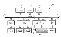
一般に、本明細書に記載された方法は、汎用コンピュータで実行され、該方法は、汎用コンピュータによって用いられるリムーバブルまたはハード媒体の指示一式として、コード化されてもよい。図5を参照すると、本発明の好ましい実施例による、集積回路チップ内のボルテージアイランド上で電力ルーティングを行なうための汎用コンピュータのブロック図が示されている。図示されるように、コンピュータシステム40は、システムバス50を介して、ランダムアクセスメモリー(RAM)42および読み出し専用メモリ(ROM)43に相互連結されたプロセッサー41を含む。プロセッサー41は、また、リムーバブル記憶装置46および大容量記憶装置45を接続するための入力/出力(I/O)アダプター44、キーボード49およびマウス48を接続するためのユーザーインタフェースアダプター47、データポート52を接続するためのポートアダプター51、およびディスプレイ装置54を接続するためのディスプレイアダプター53に相互に連結される。
In general, the methods described herein are performed on a general purpose computer, which may be encoded as a set of removable or hard media instructions used by the general purpose computer. Referring to FIG. 5, a block diagram of a general purpose computer for performing power routing on a voltage island in an integrated circuit chip is shown in accordance with a preferred embodiment of the present invention. As shown, the
ROM43は、コンピュータシステム40のための基本オペレーティングシステムを含む。リムーバブル記憶装置46の例としては、フロッピー(R)(R)ドライブ、テープドライブおよびCD−ROMドライブが挙げられる。大容量記憶装置45の例としては、ハードディスクドライブ,およびフラッシュメモリーなどの不揮発性メモリが挙げられる。キーボード49およびマウス48に加えて、トラックボール、書き込みタブレット、圧力パッド、マイクロホン、ライトペンおよび位置検知スクリーン表示装置などの他のユーザ入力装置もユーザーインタフェース47に接続されていてもよい。ディスプレイ装置の例としては、陰極線管(CRT)および液晶ディスプレイ(LCD)が挙げられる。
本発明は、充分に機能的なコンピュータシステムの文脈において記載されているが、本発明のメカニズムが、様々な形態でプログラムとして割り当てられることができ、かつ、本発明が、実際に割り当てを実行するために利用される特殊なタイプの信号伝達媒体にかかわらず等しく適用されることを当業者が認識することを留意することも重要である。信号伝達媒体の例としては、限定されることなく、フロッピー(R)ディスクまたはCDROMなどの記録可能媒体およびアナログまたはデジタル通信リンクなどの送信媒体が挙げられる。 Although the present invention has been described in the context of a fully functional computer system, the mechanisms of the present invention can be assigned as programs in various forms and the present invention actually performs the assignment. It is also important to note that those skilled in the art will recognize that the invention applies equally regardless of the particular type of signaling medium utilized. Examples of signal transmission media include, but are not limited to, recordable media such as floppy disk or CDROM, and transmission media such as analog or digital communication links.
本発明が、好ましい実施例に関して特に示され記載される一方、形態および詳細の様々な変更が、本発明の精神および範囲から逸脱することなく、行なわれてもよいことが当業者によって理解される。 While the invention has been particularly shown and described with respect to preferred embodiments, it will be understood by those skilled in the art that various changes in form and detail may be made without departing from the spirit and scope of the invention. .
本発明は、それ自体、用途、さらに目的および利点の好ましい形態と同様に、添付の図面とともに具体的な実施例の以下の詳細な説明を参照して最も理解される。 The present invention is best understood by reference to the following detailed description of specific embodiments, taken in conjunction with the accompanying drawings, as well as preferred forms of use, further objects and advantages.
Claims (15)
金属レベル1からN−1においてボルテージアイランドのための第1のロバスト電力網を生成するステップと、
金属レベルN以上において前記ボルテージアイランドのための第2のロバスト電力網を生成するステップと、
複数の電源から前記第2のロバスト電力網まで、複数の最短距離接続のルートを決めるステップとを含み、
前記第2のロバスト電力網を生成するステップは、さらに、
チップ上に同一電圧極性の電源シェイプの総数を得るステップと、
前記ボルテージアイランドが位置するチップ位置を識別するステップと、
前記電力ルーティングが行われる前記ボルテージアイランド上面に境界領域を決めて生成するステップと、
前記境界領域内に電力網を生成するステップと
を含むことを特徴とする方法。A method for performing power routing on a voltage island in an integrated circuit chip, comprising:
Generating a first robust power grid for voltage islands at metal levels 1 to N−1;
Generating a second robust power grid for the voltage island at metal level N or higher;
Routing a plurality of shortest distance connections from a plurality of power sources to the second robust power network,
Generating the second robust power network further comprises:
Obtaining a total number of power supply shapes of the same voltage polarity on the chip;
Identifying a chip location where the voltage island is located;
Determining and generating a boundary region on the upper surface of the voltage island where the power routing is performed;
Generating a power grid in the boundary region.
金属レベル1からN−1においてボルテージアイランドのための第1のロバスト電力網を生成するステップと、
金属レベルN以上において前記ボルテージアイランドのための第2のロバスト電力網を生成するステップと、
複数の電源から前記第2のロバスト電力網まで、複数の最短距離接続のルートを決めるステップとを含み、
ルーティングは、さらに、
複数のソースポイントを得て、グループAを形成するステップと、
ソース情報ごとの接続に基づいて、前記クループAを分割するステップと、
金属レベルN以上において前記第2のロバスト電力網のためのターゲット電力シェイプを得て、グループBを構築するステップと、
前記グループAの所定シェイプsのために、シェイプルーティングを行って、前記グループBでsからシェイプtまでルートを決めるステップと
を含むことを特徴とする方法。A method for performing power routing on a voltage island in an integrated circuit chip, comprising:
Generating a first robust power grid for voltage islands at metal levels 1 to N−1;
Generating a second robust power grid for the voltage island at metal level N or higher;
Routing a plurality of shortest distance connections from a plurality of power sources to the second robust power network,
Routing further
Obtaining a plurality of source points to form group A;
Dividing the group A based on connections for each source information;
Obtaining a target power shape for the second robust power grid at metal level N or higher and building group B;
Performing a shape routing for the predetermined shape s of group A to determine a route from s to shape t in group B.
金属レベル1からN−1においてボルテージアイランドのための第1のロバスト電力網を生成するプログラムコード手段と、
金属レベルN以上において前記ボルテージアイランドのための第2のロバスト電力網を生成するプログラムコード手段と、
前記第2のロバスト電力網の境界領域を決めるプログラムコード手段と、
複数の電源から前記第2のロバスト電力網まで、複数の最短距離接続のルートを決めるプログラムコード手段とを機能させ、
前記第2のロバスト電力網を生成する前記プログラムコード手段は、さらに、
チップ上の同一電圧極性の電源シェイプの総数を得るプログラムコード手段と、
前記ボルテージアイランドが位置するチップ位置を識別するプログラムコード手段と、
前記電力ルーティングが行なわれる前記ボルテージアイランド上面に境界領域を決めて生成するプログラムコード手段と、
前記境界領域内で電力網を生成するプログラムコード手段とを含む、コンピュータプログラム。A computer program for performing power routing on a voltage island in an integrated circuit chip,
Program code means for generating a first robust power grid for voltage islands at metal levels 1 to N-1;
Program code means for generating a second robust power grid for the voltage island at metal level N or higher;
Program code means for determining a boundary region of the second robust power network;
Program code means for determining a plurality of shortest distance connection routes from a plurality of power sources to the second robust power network;
The program code means for generating the second robust power network further comprises:
Program code means for obtaining the total number of power supply shapes of the same voltage polarity on the chip;
Program code means for identifying the chip position where the voltage island is located;
Program code means for determining and generating a boundary region on the upper surface of the voltage island where the power routing is performed;
A computer program comprising program code means for generating a power network within the boundary region.
金属レベル1からN−1においてボルテージアイランドのための第1のロバスト電力網を生成するプログラムコード手段と、
金属レベルN以上において前記ボルテージアイランドのための第2のロバスト電力網を生成するプログラムコード手段と、
前記第2のロバスト電力網の境界領域を決めるプログラムコード手段と、
複数の電源から前記第2のロバスト電力網まで、複数の最短距離接続のルートを決めるプログラムコード手段とを機能させ、
前記ルートを決めるプログラムコード手段は、
複数のソースポイントを得て、グループAを形成するプログラムコード手段と、
ソース情報ごとの接続に基づいて前記グループAを分割するプログラムコード手段と、
金属レベルN以上において前記第2のロバスト電力網のためのターゲット電力シェイプを得てグループBを構築するプログラムコード手段と、
前記グループAの所定シェイプsのために、シェイプルーティングを行って、前記グループBでsからシェイプtまでルートを決めるプログラムコード手段とを含む、コンピュータプログラム。A computer program for performing power routing on a voltage island in an integrated circuit chip,
Program code means for generating a first robust power grid for voltage islands at metal levels 1 to N-1;
Program code means for generating a second robust power grid for the voltage island at metal level N or higher;
Program code means for determining a boundary region of the second robust power network;
Program code means for determining a plurality of shortest distance connection routes from a plurality of power sources to the second robust power network;
The program code means for determining the route is:
Program code means for obtaining a plurality of source points and forming group A;
Program code means for dividing the group A based on connection for each source information;
Program code means for obtaining a target power shape for the second robust power grid at a metal level N or higher and building group B;
A program code means for performing shape routing for the predetermined shape s of the group A and determining a route from s to the shape t in the group B.
金属レベル1からN−1においてボルテージアイランドのための第1のロバスト電力網を生成する手段と、
金属レベルN以上において前記ボルテージアイランドのための第2のロバスト電力網を生成する手段と、
前記第2のロバスト電力網の境界領域を決める手段と、
複数の電源から前記第2のロバスト電力網まで、複数の最短距離接続のルートを決める手段とを含み、
前記第2のロバスト電力網を生成する手段は、さらに、
チップ上に同一電圧極性の電源シェイプの総数を得る手段と、
前記ボルテージアイランドが位置するチップ位置を識別する手段と、
前記電力ルーティングが行なわれる前記ボルテージアイランド上面に境界領域を決めて生成する手段と、
前記境界領域内で電力網を生成する手段と
を含むことを特徴とするコンピュータシステム。A computer system for performing power routing on a voltage island in an integrated circuit chip,
Means for generating a first robust power grid for voltage islands at metal levels 1 to N-1;
Means for generating a second robust power network for the voltage island at metal level N or higher;
Means for determining a boundary region of the second robust power network;
A plurality of shortest distance connection routes from a plurality of power sources to the second robust power network,
The means for generating the second robust power network further includes:
Means for obtaining the total number of power supply shapes of the same voltage polarity on the chip;
Means for identifying a chip position where the voltage island is located;
Means for determining and generating a boundary region on the upper surface of the voltage island where the power routing is performed;
Means for generating a power network within the boundary region.
金属レベル1からN−1においてボルテージアイランドのための第1のロバスト電力網を生成する手段と、
金属レベルN以上において前記ボルテージアイランドのための第2のロバスト電力網を生成する手段と、
前記第2のロバスト電力網の境界領域を決める手段と、
複数の電源から前記第2のロバスト電力網まで、複数の最短距離接続のルートを決める手段とを含み、
前記ルートを決める手段は、さらに、
複数のソースポイントを得て、グループAを形成する手段と、
ソース情報ごとの接続に基づいて、前記グループAを分割する手段と、
金属レベルN以上において前記第2のロバスト電力網のためのターゲット電力シェイプを得て、グループBを構築する手段と、
前記グループAで所定シェイプsのために、シェイプルーティングを行って、前記グループBでsからシェイプtまでルートを決める手段と
を含むことを特徴とするコンピュータシステム。A computer system for performing power routing on a voltage island in an integrated circuit chip,
Means for generating a first robust power grid for voltage islands at metal levels 1 to N-1;
Means for generating a second robust power network for the voltage island at metal level N or higher;
Means for determining a boundary region of the second robust power network;
A plurality of shortest distance connection routes from a plurality of power sources to the second robust power network,
The means for determining the route further includes:
Means for obtaining a plurality of source points to form group A;
Means for dividing the group A based on connection for each source information;
Means for obtaining a target power shape for said second robust power grid at metal level N or higher and building group B;
Means for carrying out shape routing for the predetermined shape s in the group A and determining a route from s to the shape t in the group B.
Applications Claiming Priority (2)
| Application Number | Priority Date | Filing Date | Title |
|---|---|---|---|
| US10/605,569 US6861753B1 (en) | 2003-10-09 | 2003-10-09 | Method and apparatus for performing power routing on a voltage island within an integrated circuit chip |
| PCT/US2004/033384 WO2005036606A2 (en) | 2003-10-09 | 2004-10-08 | Method and apparatus for performing power routing on a voltage island within an integrated circuit chip |
Publications (3)
| Publication Number | Publication Date |
|---|---|
| JP2007508701A JP2007508701A (en) | 2007-04-05 |
| JP2007508701A5 JP2007508701A5 (en) | 2007-11-08 |
| JP4456606B2 true JP4456606B2 (en) | 2010-04-28 |
Family
ID=34193454
Family Applications (1)
| Application Number | Title | Priority Date | Filing Date |
|---|---|---|---|
| JP2006534426A Expired - Fee Related JP4456606B2 (en) | 2003-10-09 | 2004-10-08 | Method, computer program, and system for performing power routing on a voltage island in an integrated circuit chip |
Country Status (6)
| Country | Link |
|---|---|
| US (2) | US6861753B1 (en) |
| EP (1) | EP1671339A4 (en) |
| JP (1) | JP4456606B2 (en) |
| KR (1) | KR100850414B1 (en) |
| CN (1) | CN100429664C (en) |
| WO (1) | WO2005036606A2 (en) |
Families Citing this family (16)
| Publication number | Priority date | Publication date | Assignee | Title |
|---|---|---|---|---|
| US7984398B1 (en) * | 2004-07-19 | 2011-07-19 | Synopsys, Inc. | Automated multiple voltage/power state design process and chip description system |
| EP1638145A1 (en) * | 2004-09-20 | 2006-03-22 | Infineon Technologies AG | Embedded switchable power ring |
| WO2006062505A1 (en) * | 2004-12-06 | 2006-06-15 | Bae Systems Information And Electronic Systems Integration Inc. | Asic device with multiple power supply voltages |
| DE102005009163B4 (en) * | 2005-02-25 | 2013-08-14 | Infineon Technologies Ag | Semiconductor device having a semiconductor chip having signal contact surfaces and supply contact surfaces, and method for producing the semiconductor device |
| JP5528662B2 (en) | 2007-09-18 | 2014-06-25 | ソニー株式会社 | Semiconductor integrated circuit |
| TWI445150B (en) * | 2007-11-15 | 2014-07-11 | Realtek Semiconductor Corp | A power mesh arrangement method utilized in an integrated circuit having multiple power domains |
| US8161446B2 (en) * | 2008-09-23 | 2012-04-17 | Qualcomm Incorporated | System and method of connecting a macro cell to a system power supply |
| US8407635B2 (en) * | 2011-01-31 | 2013-03-26 | Cadence Design Systems, Inc. | System and method for automatic extraction of power intent from custom analog/custom digital/mixed signal schematic designs |
| CN102902347B (en) * | 2012-09-28 | 2015-08-19 | 宁波大学 | A kind of Low-power-consumptiovoltage voltage island division methods of SOC (system on a chip) |
| CN103077278B (en) * | 2013-01-06 | 2015-11-18 | 宁波大学 | A kind of voltage island energization pins distribution method of SOC (system on a chip) |
| KR101538458B1 (en) | 2014-01-03 | 2015-07-23 | 연세대학교 산학협력단 | Voltage island formation for 3d many-core chip multiprocessor |
| US10318694B2 (en) | 2016-11-18 | 2019-06-11 | Qualcomm Incorporated | Adaptive multi-tier power distribution grids for integrated circuits |
| US10366199B2 (en) * | 2017-04-11 | 2019-07-30 | Qualcomm Incorporated | Cell-based power grid (PG) architecture |
| US10235491B2 (en) * | 2017-05-17 | 2019-03-19 | International Business Machines Corporation | Dynamic route keep-out in printed circuit board design |
| US10629533B2 (en) * | 2018-03-13 | 2020-04-21 | Toshiba Memory Corporation | Power island segmentation for selective bond-out |
| CN111368493B (en) * | 2018-12-26 | 2023-03-14 | 杭州广立微电子股份有限公司 | Automatic layout wiring generation method based on sparse grid |
Family Cites Families (7)
| Publication number | Priority date | Publication date | Assignee | Title |
|---|---|---|---|---|
| US6792582B1 (en) * | 2000-11-15 | 2004-09-14 | International Business Machines Corporation | Concurrent logical and physical construction of voltage islands for mixed supply voltage designs |
| US6598206B2 (en) * | 2001-05-10 | 2003-07-22 | International Business Machines Corporation | Method and system of modifying integrated circuit power rails |
| US6523150B1 (en) * | 2001-09-28 | 2003-02-18 | International Business Machines Corporation | Method of designing a voltage partitioned wirebond package |
| US6493859B1 (en) | 2001-10-01 | 2002-12-10 | International Business Machines Corporation | Method of wiring power service terminals to a power network in a semiconductor integrated circuit |
| US6538314B1 (en) * | 2002-03-29 | 2003-03-25 | International Business Machines Corporation | Power grid wiring for semiconductor devices having voltage islands |
| US6779163B2 (en) * | 2002-09-25 | 2004-08-17 | International Business Machines Corporation | Voltage island design planning |
| US6820240B2 (en) * | 2002-09-25 | 2004-11-16 | International Business Machines Corporation | Voltage island chip implementation |
-
2003
- 2003-10-09 US US10/605,569 patent/US6861753B1/en not_active Expired - Fee Related
-
2004
- 2004-10-08 JP JP2006534426A patent/JP4456606B2/en not_active Expired - Fee Related
- 2004-10-08 CN CNB2004800290278A patent/CN100429664C/en not_active Expired - Fee Related
- 2004-10-08 WO PCT/US2004/033384 patent/WO2005036606A2/en active Application Filing
- 2004-10-08 KR KR1020067006462A patent/KR100850414B1/en not_active IP Right Cessation
- 2004-10-08 EP EP04794665A patent/EP1671339A4/en not_active Withdrawn
- 2004-11-03 US US10/980,575 patent/US7234124B2/en not_active Expired - Fee Related
Also Published As
| Publication number | Publication date |
|---|---|
| JP2007508701A (en) | 2007-04-05 |
| US20050120322A1 (en) | 2005-06-02 |
| EP1671339A4 (en) | 2007-11-21 |
| US7234124B2 (en) | 2007-06-19 |
| CN100429664C (en) | 2008-10-29 |
| CN1906617A (en) | 2007-01-31 |
| KR100850414B1 (en) | 2008-08-04 |
| WO2005036606A2 (en) | 2005-04-21 |
| US6861753B1 (en) | 2005-03-01 |
| EP1671339A2 (en) | 2006-06-21 |
| WO2005036606A3 (en) | 2006-09-21 |
| KR20060132566A (en) | 2006-12-21 |
Similar Documents
| Publication | Publication Date | Title |
|---|---|---|
| JP4456606B2 (en) | Method, computer program, and system for performing power routing on a voltage island in an integrated circuit chip | |
| US6539529B2 (en) | Method and apparatus for designing integrated circuits and storage medium for storing the method | |
| US6598206B2 (en) | Method and system of modifying integrated circuit power rails | |
| US6546538B1 (en) | Integrated circuit having on-chip capacitors for supplying power to portions of the circuit requiring high-transient peak power | |
| US6493859B1 (en) | Method of wiring power service terminals to a power network in a semiconductor integrated circuit | |
| JP2009087974A (en) | Semiconductor device and layout method thereof | |
| JPH0644596B2 (en) | Method of forming CMOS cell layout | |
| JP2002373939A (en) | Method, apparatus, and program for designing clock distribution circuit and computer-readable record medium recording the program | |
| JP2003330987A (en) | Layout method of semiconductor integrated circuit and semiconductor integrated circuit | |
| JP3006824B2 (en) | Wiring design method and wiring design device | |
| EP1638145A1 (en) | Embedded switchable power ring | |
| US10216886B2 (en) | Semiconductor device and method for designing a semiconductor device | |
| KR20020077040A (en) | Semiconductor integrated circuit configured to supply sufficient internal current | |
| JP4987787B2 (en) | Placement verification device | |
| US6588003B1 (en) | Method of control cell placement for datapath macros in integrated circuit designs | |
| JP2006332516A (en) | Method and apparatus of automatically designing semiconductor device | |
| JP3169069B2 (en) | Hierarchical layout system for semiconductor integrated circuit, layout method, and storage medium in which this is written | |
| JP2003338545A (en) | Wiring method for semiconductor integrated circuit | |
| JP2008270439A (en) | Electrode arrangement method for semiconductor device | |
| JP2002237522A (en) | Recording media with program for making shield wiring, the program and lsi | |
| JPH1117157A (en) | Floor-plane layout system | |
| JP2002203001A (en) | Equipment for designing layout of power line | |
| JPH10135339A (en) | Automatic layout wiring method | |
| JPWO2018139408A1 (en) | Design support system and design support method | |
| JP2000058660A (en) | Method and device for automatic wiring of semiconductor, and medium where semiconductor automatic wiring program is recorded |
Legal Events
| Date | Code | Title | Description |
|---|---|---|---|
| A521 | Written amendment |
Free format text: JAPANESE INTERMEDIATE CODE: A523 Effective date: 20070921 |
|
| A621 | Written request for application examination |
Free format text: JAPANESE INTERMEDIATE CODE: A621 Effective date: 20070921 |
|
| A977 | Report on retrieval |
Free format text: JAPANESE INTERMEDIATE CODE: A971007 Effective date: 20090123 |
|
| A131 | Notification of reasons for refusal |
Free format text: JAPANESE INTERMEDIATE CODE: A131 Effective date: 20090630 |
|
| RD12 | Notification of acceptance of power of sub attorney |
Free format text: JAPANESE INTERMEDIATE CODE: A7432 Effective date: 20090728 |
|
| A521 | Written amendment |
Free format text: JAPANESE INTERMEDIATE CODE: A821 Effective date: 20090728 |
|
| A521 | Written amendment |
Free format text: JAPANESE INTERMEDIATE CODE: A523 Effective date: 20090911 |
|
| A131 | Notification of reasons for refusal |
Free format text: JAPANESE INTERMEDIATE CODE: A131 Effective date: 20091013 |
|
| A521 | Written amendment |
Free format text: JAPANESE INTERMEDIATE CODE: A523 Effective date: 20100108 |
|
| TRDD | Decision of grant or rejection written | ||
| A01 | Written decision to grant a patent or to grant a registration (utility model) |
Free format text: JAPANESE INTERMEDIATE CODE: A01 Effective date: 20100202 |
|
| RD14 | Notification of resignation of power of sub attorney |
Free format text: JAPANESE INTERMEDIATE CODE: A7434 Effective date: 20100202 |
|
| A01 | Written decision to grant a patent or to grant a registration (utility model) |
Free format text: JAPANESE INTERMEDIATE CODE: A01 |
|
| A61 | First payment of annual fees (during grant procedure) |
Free format text: JAPANESE INTERMEDIATE CODE: A61 Effective date: 20100205 |
|
| FPAY | Renewal fee payment (event date is renewal date of database) |
Free format text: PAYMENT UNTIL: 20130212 Year of fee payment: 3 |
|
| R150 | Certificate of patent or registration of utility model |
Free format text: JAPANESE INTERMEDIATE CODE: R150 |
|
| FPAY | Renewal fee payment (event date is renewal date of database) |
Free format text: PAYMENT UNTIL: 20130212 Year of fee payment: 3 |
|
| FPAY | Renewal fee payment (event date is renewal date of database) |
Free format text: PAYMENT UNTIL: 20140212 Year of fee payment: 4 |
|
| LAPS | Cancellation because of no payment of annual fees |