JP5528662B2 - Semiconductor integrated circuit - Google Patents
Semiconductor integrated circuit Download PDFInfo
- Publication number
- JP5528662B2 JP5528662B2 JP2007241517A JP2007241517A JP5528662B2 JP 5528662 B2 JP5528662 B2 JP 5528662B2 JP 2007241517 A JP2007241517 A JP 2007241517A JP 2007241517 A JP2007241517 A JP 2007241517A JP 5528662 B2 JP5528662 B2 JP 5528662B2
- Authority
- JP
- Japan
- Prior art keywords
- switch
- line
- block
- voltage
- semiconductor integrated
- Prior art date
- Legal status (The legal status is an assumption and is not a legal conclusion. Google has not performed a legal analysis and makes no representation as to the accuracy of the status listed.)
- Active
Links
- 239000004065 semiconductor Substances 0.000 title claims description 34
- 238000013461 design Methods 0.000 description 18
- 238000010586 diagram Methods 0.000 description 18
- 230000008859 change Effects 0.000 description 12
- 230000008901 benefit Effects 0.000 description 8
- 101100033865 Saccharomyces cerevisiae (strain ATCC 204508 / S288c) RFA1 gene Proteins 0.000 description 6
- 101100524516 Saccharomyces cerevisiae (strain ATCC 204508 / S288c) RFA2 gene Proteins 0.000 description 6
- 238000005516 engineering process Methods 0.000 description 6
- 230000000694 effects Effects 0.000 description 5
- 238000000034 method Methods 0.000 description 5
- 239000002184 metal Substances 0.000 description 4
- 230000002093 peripheral effect Effects 0.000 description 4
- 230000004913 activation Effects 0.000 description 2
- 238000012217 deletion Methods 0.000 description 2
- 230000037430 deletion Effects 0.000 description 2
- 230000006870 function Effects 0.000 description 2
- 238000003780 insertion Methods 0.000 description 2
- 230000037431 insertion Effects 0.000 description 2
- 238000002955 isolation Methods 0.000 description 2
- 239000011159 matrix material Substances 0.000 description 2
- 230000009467 reduction Effects 0.000 description 2
- 239000002699 waste material Substances 0.000 description 2
- 230000002411 adverse Effects 0.000 description 1
- 230000002238 attenuated effect Effects 0.000 description 1
- 230000005540 biological transmission Effects 0.000 description 1
- 230000000295 complement effect Effects 0.000 description 1
- 239000004020 conductor Substances 0.000 description 1
- 230000009849 deactivation Effects 0.000 description 1
- 239000012535 impurity Substances 0.000 description 1
- 238000004519 manufacturing process Methods 0.000 description 1
- 229910044991 metal oxide Inorganic materials 0.000 description 1
- 150000004706 metal oxides Chemical class 0.000 description 1
- 238000012946 outsourcing Methods 0.000 description 1
- 238000012545 processing Methods 0.000 description 1
- 238000007493 shaping process Methods 0.000 description 1
Images


Classifications
-
- H—ELECTRICITY
- H03—ELECTRONIC CIRCUITRY
- H03K—PULSE TECHNIQUE
- H03K17/00—Electronic switching or gating, i.e. not by contact-making and –breaking
- H03K17/51—Electronic switching or gating, i.e. not by contact-making and –breaking characterised by the components used
- H03K17/56—Electronic switching or gating, i.e. not by contact-making and –breaking characterised by the components used by the use, as active elements, of semiconductor devices
- H03K17/687—Electronic switching or gating, i.e. not by contact-making and –breaking characterised by the components used by the use, as active elements, of semiconductor devices the devices being field-effect transistors
- H03K17/6871—Electronic switching or gating, i.e. not by contact-making and –breaking characterised by the components used by the use, as active elements, of semiconductor devices the devices being field-effect transistors the output circuit comprising more than one controlled field-effect transistor
- H03K17/6872—Electronic switching or gating, i.e. not by contact-making and –breaking characterised by the components used by the use, as active elements, of semiconductor devices the devices being field-effect transistors the output circuit comprising more than one controlled field-effect transistor using complementary field-effect transistors
-
- H—ELECTRICITY
- H01—ELECTRIC ELEMENTS
- H01L—SEMICONDUCTOR DEVICES NOT COVERED BY CLASS H10
- H01L27/00—Devices consisting of a plurality of semiconductor or other solid-state components formed in or on a common substrate
- H01L27/02—Devices consisting of a plurality of semiconductor or other solid-state components formed in or on a common substrate including semiconductor components specially adapted for rectifying, oscillating, amplifying or switching and having potential barriers; including integrated passive circuit elements having potential barriers
- H01L27/0203—Particular design considerations for integrated circuits
- H01L27/0207—Geometrical layout of the components, e.g. computer aided design; custom LSI, semi-custom LSI, standard cell technique
-
- H—ELECTRICITY
- H01—ELECTRIC ELEMENTS
- H01L—SEMICONDUCTOR DEVICES NOT COVERED BY CLASS H10
- H01L27/00—Devices consisting of a plurality of semiconductor or other solid-state components formed in or on a common substrate
- H01L27/02—Devices consisting of a plurality of semiconductor or other solid-state components formed in or on a common substrate including semiconductor components specially adapted for rectifying, oscillating, amplifying or switching and having potential barriers; including integrated passive circuit elements having potential barriers
- H01L27/04—Devices consisting of a plurality of semiconductor or other solid-state components formed in or on a common substrate including semiconductor components specially adapted for rectifying, oscillating, amplifying or switching and having potential barriers; including integrated passive circuit elements having potential barriers the substrate being a semiconductor body
- H01L27/08—Devices consisting of a plurality of semiconductor or other solid-state components formed in or on a common substrate including semiconductor components specially adapted for rectifying, oscillating, amplifying or switching and having potential barriers; including integrated passive circuit elements having potential barriers the substrate being a semiconductor body including only semiconductor components of a single kind
- H01L27/085—Devices consisting of a plurality of semiconductor or other solid-state components formed in or on a common substrate including semiconductor components specially adapted for rectifying, oscillating, amplifying or switching and having potential barriers; including integrated passive circuit elements having potential barriers the substrate being a semiconductor body including only semiconductor components of a single kind including field-effect components only
- H01L27/088—Devices consisting of a plurality of semiconductor or other solid-state components formed in or on a common substrate including semiconductor components specially adapted for rectifying, oscillating, amplifying or switching and having potential barriers; including integrated passive circuit elements having potential barriers the substrate being a semiconductor body including only semiconductor components of a single kind including field-effect components only the components being field-effect transistors with insulated gate
- H01L27/092—Devices consisting of a plurality of semiconductor or other solid-state components formed in or on a common substrate including semiconductor components specially adapted for rectifying, oscillating, amplifying or switching and having potential barriers; including integrated passive circuit elements having potential barriers the substrate being a semiconductor body including only semiconductor components of a single kind including field-effect components only the components being field-effect transistors with insulated gate complementary MIS field-effect transistors
-
- H—ELECTRICITY
- H03—ELECTRONIC CIRCUITRY
- H03K—PULSE TECHNIQUE
- H03K17/00—Electronic switching or gating, i.e. not by contact-making and –breaking
- H03K17/16—Modifications for eliminating interference voltages or currents
-
- H—ELECTRICITY
- H03—ELECTRONIC CIRCUITRY
- H03K—PULSE TECHNIQUE
- H03K19/00—Logic circuits, i.e. having at least two inputs acting on one output; Inverting circuits
- H03K19/0175—Coupling arrangements; Interface arrangements
- H03K19/0185—Coupling arrangements; Interface arrangements using field effect transistors only
-
- H—ELECTRICITY
- H03—ELECTRONIC CIRCUITRY
- H03K—PULSE TECHNIQUE
- H03K3/00—Circuits for generating electric pulses; Monostable, bistable or multistable circuits
- H03K3/01—Details
- H03K3/012—Modifications of generator to improve response time or to decrease power consumption
-
- H—ELECTRICITY
- H01—ELECTRIC ELEMENTS
- H01L—SEMICONDUCTOR DEVICES NOT COVERED BY CLASS H10
- H01L27/00—Devices consisting of a plurality of semiconductor or other solid-state components formed in or on a common substrate
- H01L27/02—Devices consisting of a plurality of semiconductor or other solid-state components formed in or on a common substrate including semiconductor components specially adapted for rectifying, oscillating, amplifying or switching and having potential barriers; including integrated passive circuit elements having potential barriers
- H01L27/04—Devices consisting of a plurality of semiconductor or other solid-state components formed in or on a common substrate including semiconductor components specially adapted for rectifying, oscillating, amplifying or switching and having potential barriers; including integrated passive circuit elements having potential barriers the substrate being a semiconductor body
- H01L27/10—Devices consisting of a plurality of semiconductor or other solid-state components formed in or on a common substrate including semiconductor components specially adapted for rectifying, oscillating, amplifying or switching and having potential barriers; including integrated passive circuit elements having potential barriers the substrate being a semiconductor body including a plurality of individual components in a repetitive configuration
- H01L27/118—Masterslice integrated circuits
- H01L27/11803—Masterslice integrated circuits using field effect technology
- H01L27/11807—CMOS gate arrays
Landscapes
- Engineering & Computer Science (AREA)
- Power Engineering (AREA)
- Computer Hardware Design (AREA)
- Physics & Mathematics (AREA)
- General Engineering & Computer Science (AREA)
- Condensed Matter Physics & Semiconductors (AREA)
- General Physics & Mathematics (AREA)
- Microelectronics & Electronic Packaging (AREA)
- Computing Systems (AREA)
- Mathematical Physics (AREA)
- Semiconductor Integrated Circuits (AREA)
- Design And Manufacture Of Integrated Circuits (AREA)
Description
本発明は、回路ブロックの内部電圧線と、電源電圧または基準電圧が印加される配線との接続と非接続をスイッチにより制御する半導体集積回路に関する。 The present invention relates to a semiconductor integrated circuit that controls connection and non-connection of an internal voltage line of a circuit block and a wiring to which a power supply voltage or a reference voltage is applied by a switch.
回路に対しスイッチにより電源供給の遮断とその解除を制御するものとして、MTCMOS(Multi-threshold Complementary Metal Oxide Semiconductor)技術が知られている。
一般的に、電源電圧低下や素子微細化に付随して信号遅延が発生しないように、論理回路等のトランジスタの閾値電圧を設計値として下げる必要がある。論理回路等のトランジスタの閾値電圧が小さいとリーク電流が大きい。MTCMOS技術は、停止状態の回路に対し、論理回路等のトランジスタに比べ、より大きな閾値電圧のトランジスタ(電源スイッチ)によって、リーク電流経路を遮断して、その消費電力の浪費を防ぐものである。
An MTCMOS (Multi-threshold Complementary Metal Oxide Semiconductor) technique is known as a circuit that controls the interruption and release of power supply by a switch.
Generally, it is necessary to lower the threshold voltage of a transistor such as a logic circuit as a design value so that signal delay does not occur accompanying power supply voltage reduction or element miniaturization. When the threshold voltage of a transistor such as a logic circuit is small, the leakage current is large. In the MTCMOS technology, a leakage current path is blocked by a transistor (power switch) having a larger threshold voltage than a transistor such as a logic circuit in a stopped state, thereby preventing waste of power consumption.
MTCMOS技術の回路ブロックへの適用では、いわゆる仮想VDD線、仮想GND線と称される、回路ブロック内に設けられた内部電圧線を設ける。内部電圧線は、回路ブロックの外部でブロック間接続を行うグローバルな実電源線(実VDD線)や実基準電圧線(実VSS線)に対して、電源遮断とその解除のための電源スイッチを介して接続される。
電源スイッチを設ける箇所は、起動と停止が繰り返される機能回路と実VDD線との間、機能回路と実VSS線との間、その両方の3通りがあり、スイッチとしては通常、VDD側ではPMOSトランジスタ、VSS線側ではNMOSトランジスタを用いる。
In application of the MTCMOS technology to a circuit block, an internal voltage line provided in the circuit block, which is called a virtual VDD line or a virtual GND line, is provided. The internal voltage line has a power switch for shutting off and releasing the power supply for the global real power line (real VDD line) and real reference voltage line (real VSS line) that connect the blocks outside the circuit block. Connected through.
There are three power switch locations: between the functional circuit that is repeatedly activated and deactivated and the actual VDD line, and between the functional circuit and the actual VSS line. An NMOS transistor is used on the transistor and VSS line side.
MTCMOS適用ブロックの機能回路の起動と停止は、半導体集積回路が起動された後は常時、実VDD線と実VSS線からの電源供給を受けて動作状態におかれるMTCMOS非適用ブロック内の回路によって制御される。あるいは、MTCMOS適用ブロックの機能回路の起動と停止を制御する制御信号を、半導体集積回路の外部端子から入力可能な構成が採用されることもある。 The activation and deactivation of the functional circuit of the MTCMOS application block is performed by a circuit in the MTCMOS non-application block that is always in operation after receiving power supply from the actual VDD line and the actual VSS line after the semiconductor integrated circuit is activated. Be controlled. Alternatively, a configuration may be employed in which a control signal for controlling activation and stop of the functional circuit of the MTCMOS application block can be input from an external terminal of the semiconductor integrated circuit.
ところで、電源スイッチは、MTCMOS適用ブロック内セルにより実現されることがある。より詳細にはMTCMOS適用ブロック内において、インバータ、NAND回路、NOR回路等の各論理回路セル内に、あるいは、幾つかの論理回路で実現される機能回路セル内に電源スイッチを設ける場合と、論理回路や機能回路を有しない専用の電源スイッチセルを設ける場合がある。以下、このタイプのスイッチ配置を「内部スイッチ(SW)配置」、当該配置が採られた半導体集積回路を「内部SW配置型IC」と称する。 By the way, the power switch may be realized by a cell in an MTCMOS application block. More specifically, in the MTCMOS application block, when a power switch is provided in each logic circuit cell such as an inverter, NAND circuit, NOR circuit, etc., or in a functional circuit cell realized by several logic circuits, A dedicated power switch cell that does not have a circuit or a functional circuit may be provided. Hereinafter, this type of switch arrangement is referred to as an “internal switch (SW) arrangement”, and a semiconductor integrated circuit employing the arrangement is referred to as an “internal SW arrangement type IC”.
内部SW配置型ICに対して、電源供給制御対象の回路ブロックの周囲に電源スイッチを配置した半導体集積回路が知られている(例えば、特許文献1、特許文献2参照)。このタイプのスイッチ配置を「外部SW配置」、当該配置が採られた半導体集積回路を「外部SW配置型IC」と称する。
外部SW配置は、いわゆる「マクロ」と称される汎用的な回路(例えばメモリやCPU等)を一部または全部とする回路ブロックと組み合わせて好適に用いられる。
A semiconductor integrated circuit is known in which a power switch is arranged around a circuit block to be controlled for power supply with respect to an internal SW arrangement IC (see, for example,
The external SW arrangement is suitably used in combination with a circuit block that includes a general-purpose circuit (for example, a memory, a CPU, or the like) called a “macro” in part or in whole.
上記特許文献2には、回路ブロックの3辺又は4辺に対し、長手方向が各辺に沿う形状のトランジスタセル(スイッチ)が配置され、当該スイッチ内のトランジスタゲートラインの配置方向が上記長手方向と同一な構成が開示されている。
この構成において、トランジスタセル配置領域の反回路ブロック側(外側)に、回路ブロックの周囲を環状に囲む環状線としてVDD供給リングおよびVSS供給リングが配置されている。VDD供給リングと、スイッチトランジスタのドレインとが、VDD供給リングと異なる階層のメタル配線層により接続されている。VSS供給リングと、回路ブロック内のVSS線とが、VSS供給リングと異なる階層のメタル配線層により接続されている。また、スイッチトランジスタのソースと、回路ブロック内の仮想VSS線とが、VSS供給リングと異なる階層のメタル配線層により接続されている。
In this configuration, a VDD supply ring and a VSS supply ring are arranged as annular lines surrounding the circuit block in a ring shape on the side opposite to the circuit block (outside) of the transistor cell arrangement region. The VDD supply ring and the drain of the switch transistor are connected by a metal wiring layer having a layer different from that of the VDD supply ring. The VSS supply ring and the VSS line in the circuit block are connected by a metal wiring layer having a layer different from that of the VSS supply ring. In addition, the source of the switch transistor and the virtual VSS line in the circuit block are connected by a metal wiring layer having a layer different from that of the VSS supply ring.
上記特許文献1に記載の半導体集積回路は、VDD電圧の供給線が回路ブロック(内部回路)の周囲に環状に配置されていないため、VDD電圧の供給元から遠いVDD電圧の供給線箇所で電圧ドロップが生じ、その結果、他と同じサイズのスイッチトランジスタを同じ時間だけオンまたはオフしても、内部回路の内部電圧線を充放電する能力に差が生じる。このため、VDD電圧の供給元から遠い箇所ほどスイッチトランジスタのサイズを大きくするか、トランジスタ数を増やすなどの工夫が必要となる。その結果、内部回路の停止状態においてスイッチトランジスタを介したリーク電流が増大するという不利益が生じる。
スイッチトランジスタの閾値電圧は、内部回路のトランジスタの閾値電圧より大きく設定され、相対的にリーク電流は小さい。しかし、停止期間が長いと、スイッチトランジスタのサイズや数の増大による無駄な電力消費は無視できなくなる。
In the semiconductor integrated circuit described in
The threshold voltage of the switch transistor is set larger than the threshold voltage of the transistor in the internal circuit, and the leakage current is relatively small. However, if the stop period is long, useless power consumption due to an increase in the size and number of switch transistors cannot be ignored.
上記特許文献2に記載の半導体集積回路は、VDD電圧やVSS電圧の供給線が供給リングとして環状配置されているため、供給リングがない上記特許文献1に記載の半導体集積回路と比べると、電圧の供給元から各スイッチトランジスタまでの電圧ドロップが均一化されている。よって、上記リーク電流の増大は比較的抑制される。
In the semiconductor integrated circuit described in
しかしながら、上記特許文献2に記載の半導体集積回路は、環状線(供給リング)が、スイッチトランジスタと別々に配置されているため、スイッチトランジスタと供給リング(VDD供給リングおよびVSS供給リング)を接続する配線が複雑である。
However, in the semiconductor integrated circuit described in
VDD供給リングやVSS供給リングは電圧ドロップを均一化する目的で設けられるが、その電位は、周辺の動作回路の影響を受けて完全に均一でないことがある。勿論、これらの供給リングの配線抵抗を減らすことにより、より均一になるが、頻繁に大きな振幅で動作する周辺回路の付近では、その影響を受けて、例えばVSS供給リングの電位が基準電位(例えば0[V])から持ち上がることがある。しかし、周辺回路の動作を完全に見積もることは困難であるため、周辺回路の影響を回避してスイッチトランジスタの動作の安定化を図るには、設計中に、スイッチトランジスタの位置をずらし、あるいは、サイズを変更する必要が生じ、接続配線をやり直す設計負担が大きい。 Although the VDD supply ring and the VSS supply ring are provided for the purpose of uniforming the voltage drop, the potential may not be completely uniform due to the influence of the peripheral operation circuit. Of course, by reducing the wiring resistance of these supply rings, it becomes more uniform, but in the vicinity of peripheral circuits that frequently operate with a large amplitude, for example, the potential of the VSS supply ring becomes the reference potential (for example, 0 [V]). However, since it is difficult to fully estimate the operation of the peripheral circuit, to avoid the influence of the peripheral circuit and stabilize the operation of the switch transistor, the position of the switch transistor is shifted during the design, or It is necessary to change the size, and the design burden of redoing the connection wiring is large.
つまり、特許文献2に記載のスイッチトランジスタ(当該特許文献では「マクロ」と称している)の構成は、そのような設計変更に対応した構造を有していない。
なお、スイッチトランジスタの位置やサイズが重要であることは、特許文献2においてスイッチトランジスタのサイズを変更し、あるいは、スイッチトランジスタを2重に設けるなどの様々な変更例が示されていることからも明らかである。
That is, the configuration of the switch transistor described in Patent Document 2 (referred to as “macro” in the Patent Document) does not have a structure corresponding to such a design change.
The fact that the position and size of the switch transistor are important is that, in
本発明の一形態に関わる半導体集積回路は、格子状に配置された複数の内部電圧線を備える回路ブロックと、前記回路ブロックの周囲で閉じた環状線を形成し、電源電圧または基準電圧が印加される第1環状線と、前記第1環状線と前記回路ブロックとの間で閉じた環状線を形成し、複数の箇所で前記複数の内部電圧線と電気的に接続されている第2環状線と、前記回路ブロックの周囲に配置され、それぞれが矩形の外形を備える複数のスイッチブロックと、を有し、各スイッチブロックが、当該スイッチブロック内で互いに並行な前記第1環状線と前記第2環状線との間に電気的に接続された複数のスイッチトランジスタを備え、前記複数のスイッチトランジスタの一部が、前記各スイッチブロック内において前記第1環状線と前記第2環状線の下層領域に配置され、前記各スイッチブロックの外周の4辺のうち前記回路ブロックに近い内側辺から前記第1環状線までの距離が前記複数のスイッチブロックで等しく、かつ、前記内側辺から前記第2環状線までの距離が前記複数のスイッチブロックで等しい。
好適に、前記複数のスイッチブロックは、同一サイズを有し、前記回路ブロックの辺ごとに異なる少なくとも4種類のスイッチブロックを有する。
さらに好適に、前記各スイッチブロックにおいて、前記第1環状線および第2環状線のスイッチブロック内部分である2つの電圧線セグメントと前記複数のスイッチトランジスタが内部接続され、前記各スイッチブロックのブロック枠の対向する2辺における、前記2つの電圧線セグメントの端辺の位置関係が、前記複数のスイッチブロックで同じに設定されている。
A semiconductor integrated circuit according to one embodiment of the present invention forms a circuit block having a plurality of internal voltage lines arranged in a grid and an annular line closed around the circuit block, and a power supply voltage or a reference voltage is applied A first annular line, and a second annular line that forms a closed annular line between the first annular line and the circuit block and is electrically connected to the plurality of internal voltage lines at a plurality of locations. a line, disposed around the circuit blocks, possess a plurality of switch blocks, each provided with a rectangular outer shape, and each switch block, said mutually parallel first annular line in the switch block No. A plurality of switch transistors electrically connected to each other between the first ring line and the second ring in each switch block. The distance from the inner side close to the circuit block to the first annular line among the four sides of the outer periphery of each switch block is equal in the plurality of switch blocks, and from the inner side The distance to the second annular line is equal in the plurality of switch blocks.
Preferably, the plurality of switch blocks have at least four types of switch blocks having the same size and different for each side of the circuit block.
More preferably, in each of the switch blocks, two voltage line segments, which are internal portions of the first annular line and the second annular line, and the plurality of switch transistors are internally connected, and a block frame of each switch block The positional relationship of the end sides of the two voltage line segments on the two opposing sides is set to be the same in the plurality of switch blocks.
好適に、前記回路ブロックは少なくとも2組の互いに対向する2辺を含む外周を備え、前記対向する2辺の側に配置された前記スイッチブロックが、ミラー対称または180度回転対称のパターンを有する。 Preferably, the circuit block has an outer periphery including at least two sets of two opposite sides, and the switch block arranged on the two opposite sides has a mirror-symmetrical pattern or a 180-degree rotationally symmetric pattern .
好適に、前記回路ブロックは少なくとも2組の互いに対向する2辺を含む外周を備え、少なくとも1組の前記対向する2辺において、一方の辺側と他方の辺側で前記スイッチブロックの配置数が異なる。
さらに好適に、前記回路ブロックの外周の各辺からみた、当該回路ブロックへ電源電圧または基準電圧を供給する配線のインピーダンスが小さいほど数多くなるように、前記回路ブロックの辺ごとに前記スイッチブロックの配置数が決められている。
Preferably, the circuit block includes an outer periphery including at least two sets of two sides facing each other, and at least one set of the two sides facing each other, the number of switch blocks arranged on one side and the other side is set. Different .
More preferably, the switch block is arranged for each side of the circuit block such that the smaller the impedance of the wiring for supplying the power supply voltage or the reference voltage to the circuit block as seen from each side of the outer periphery of the circuit block, the larger the number. The number is decided .
好適に、前記複数のスイッチブロック内で、前記スイッチトランジスタは、ゲート電極の長手方向が同じ方向に揃えられている。 Preferably, in the plurality of switch blocks, in the switch transistors, the longitudinal directions of the gate electrodes are aligned in the same direction .
好適に、前記スイッチブロック内の異なるスイッチトランジスタを各々が制御する複数のスイッチ制御線を有する。
さらに好適に、前記複数のスイッチ制御線の各々に対し、バッファ回路が接続されている。
さらに好適に、複数の前記バッファ回路が、前記第2環状線に対し、前記回路ブロックと反対の側に配置されている。
さらに好適に、前記各スイッチブロックにおいて、前記複数のスイッチトランジスタの配置領域と交差または近接して、前記第1環状線および第2環状線のスイッチブロック内部分である2つの電圧線セグメントが配置され、前記複数のスイッチトランジスタの配置領域および前記2つの電圧線セグメントに対し前記回路ブロックと反対の側に、前記第1環状線の電圧線セグメントから電圧供給を受けて動作する前記バッファ回路が配置され、前記バッファ回路の入力側に、制御線を介して制御信号が入力される第1制御線セグメントが配置され、前記バッファ回路の出力側に、前記スイッチトランジスタの制御ノードに電気的に接続される第2制御線セグメントが配置されている。
Preferably, a plurality of switch control lines each controlling different switch transistors in the switch block are provided .
More preferably, a buffer circuit is connected to each of the plurality of switch control lines.
More preferably, the plurality of buffer circuits are arranged on the side opposite to the circuit block with respect to the second annular line.
More preferably, in each of the switch blocks, two voltage line segments that are portions inside the switch block of the first annular line and the second annular line are arranged so as to intersect or be close to the arrangement region of the plurality of switch transistors. The buffer circuit that operates by receiving voltage supply from the voltage line segment of the first annular line is disposed on the opposite side of the circuit block with respect to the arrangement region of the plurality of switch transistors and the two voltage line segments. A first control line segment to which a control signal is input via a control line is disposed on the input side of the buffer circuit, and is electrically connected to the control node of the switch transistor on the output side of the buffer circuit A second control line segment is disposed.
前述した一形態の構成によれば、環状線が、第1および第2環状線と称する2本形成される。
このため、複数のスイッチブロックの各々において、第1環状線の一部と、第2環状線の一部とを備え、これらスイッチブロック内の第1および第2環状線にスイッチトランジスタが接続されている。また、複数のスイッチブロックにおいて、第1および第2環状線から回路ブロックまでの距離が一定である。
したがって、スイッチブロック同士を隣接させて、第1環状線(のブロック内セグメント)同士、第2環状線(のブロック内セグメント)同士をつなぐか、あるいは、距離が離れている場合には、対応する第1または第2環状線(のブロック内セグメント)同士の間を配線でつなぐことによって、回路ブロックの周囲で閉じた2本の環状線が形成される。
According to one embodiment of the above-described configuration, the ring-shaped lines are two forms, referred to as first and second ring-shaped line.
Therefore, in each of the plurality of switch blocks, a portion of the first ring-shaped line, and a part of the second ring-shaped line, the switch transistor is connected to the first and second annular line of these switches in blocks Has been. Further, a plurality of switch blocks, the distance from the first and second ring-shaped line to the circuit block is constant.
Therefore, if the switch blocks are adjacent to each other and the first annular lines (intra- block segments) are connected to each other, or the second annular lines (intra-block segments) are connected to each other, or the distance is long, it corresponds. by connecting wiring between the first or second annular line (block segments) between, two ring-shaped line closed around the circuit blocks are formed.
スイッチブロックの位置を動かす場合は、移動対象スイッチブロックの第1および第2環状線以外の構成要素を所望の位置に動かし、その移動させた位置で当該構成要素を第1および第2環状線に接続させる。
このとき上記一形態では、第1および第2環状線をスイッチブロックごとに有しているため、回路ブロックとの接続変更も不要である。このため、第1および第2環状線それぞれに対し、スイッチブロックの第1および第2環状線以外の構成要素を移動させるだけで、自由にスイッチブロックを移動できる。
When moving the position of the switch block, the first and second components other than the loop line of the moving object switch block moving to a desired position, the first and second ring-shaped line the components in a position obtained by the movement Connect to.
In this case the one embodiment, since the have a first and second ring-shaped line for each switch block, change of connection between the circuit blocks is not necessary. Therefore, for each first and second ring-shaped line, only by moving the first and second components other than the loop line of the switch block, you can move the switch block freely.
以上はスイッチトランジスタの移動における作用説明であるが、スイッチトランジスタを挿入し、あるいは、削除する場合も、同様に、スイッチブロックの第1および第2環状線以外の構成要素を必要な数だけ必要な場所に挿入、削除するだけでよい。
The above is an operational description of the movement of the switch transistor, insert the switch transistor, or may be deleted, similarly, requires the necessary number of first and second annular line other than the components of the switch block You just need to insert and delete in the right place.
本発明によれば、スイッチの移動、数の変更などに際し、主に、スイッチブロックの電圧線セグメント以外の構成要素変更で済むため、設計変更が容易で、スイッチの位置や数の最適化を行うことが簡単であるという利益が得られる。より詳細には、電源電圧または基準電圧の供給線がスイッチと離れて互いの位置関係に統一性がない場合に、スイッチ移動やスイッチの挿入、削除などの設計変更に際し、異なる階層のメタル配線層を接続し直す必要があるが、本発明では、そのような環状レール線以外の配線を一々やり直す手間が不要である。 According to the present invention, when moving or changing the number of switches, it is mainly necessary to change the components other than the voltage line segments of the switch block. Therefore, the design can be easily changed and the position and number of the switches can be optimized. The benefit is that it is easy. More specifically, when the power supply voltage or reference voltage supply line is separated from the switch and the mutual positional relationship is not uniform, the metal wiring layer at a different level is used for design changes such as switch movement, switch insertion, and deletion. However, in the present invention, there is no need to rework wiring other than the annular rail line one by one.
以下、本発明の実施形態を、図面を参照して説明する。 Embodiments of the present invention will be described below with reference to the drawings.
<全体構成>
図1に、本発明の実施形態に関わる半導体集積回路の全体構成を示す。
図1において、半導体集積回路が形成される矩形半導体チップの4つの辺に沿って、それぞれ複数の入出力セル40が列をなして配列されている。
<Overall configuration>
FIG. 1 shows the overall configuration of a semiconductor integrated circuit according to an embodiment of the present invention.
In FIG. 1, a plurality of input /
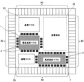
図1に示す入出力セル40に四方を囲まれた回路配置のためのチップエリアに、いくつかの回路ブロックが配置されている。図1に示す例では、「通電領域」と称される、半導体集積回路のベーシックな構成、例えば、CPU、レジスタ、メモリ、電源回路などを含む通電回路ブロック32がチップエリアに配置されている。通電回路ブロック32は、MTCMOS技術の非適用回路ブロックに対応し、当該半導体集積回路が起動後は常時、電源電圧VDDと基準電圧VSSの供給を受けて動作する。
回路配置のためのチップエリアには、さらに、「マクロ」と称され、他の半導体集積回路で流用可能に個別設計される汎用的な回路を一部または全部に含む回路ブロックが多数配置されている。「マクロ」は、外部委託による設計が可能であり、またIP(Intellectual Property)として他社から購入することも可能である。
Several circuit blocks are arranged in a chip area for circuit arrangement surrounded by the input /
In the chip area for circuit arrangement, a number of circuit blocks including part or all of general-purpose circuits that are individually designed to be diverted in other semiconductor integrated circuits are arranged. Yes. The “macro” can be designed by outsourcing and can be purchased from other companies as an IP (Intellectual Property).
「マクロ」としての回路ブロックは、通電回路ブロック32と同様に、当該半導体集積回路が起動後は常時、電源電圧VDDと基準電圧VSSの供給を受けて動作する「通電マクロ」と称されるMTCMOS技術が非適用の非適用回路ブロック33と、「電源遮断マクロ」と称され、MTCMOS技術が適用されて、必要に応じて適宜電源遮断が行われる電源遮断対象の回路ブロック1と、に大別できる。
なお、入出力セル40に囲まれたチップエリアに配置された通電回路ブロック32、非適用回路ブロック33および電源遮断対象の回路ブロック1は、図1では図示を省略しているが、実VDD線と実VSS線が対をなして配置され、これにより電源供給を受ける。より詳細には、入出力セル40の幾つかが電源供給のために割り当てられており、当該電源供給のための入出力セル40から、チップエリア内のロウ(行)方向とカラム(列)方向にそれぞれ実電源線対が配線され、これにより、通電回路ブロック32、非適用回路ブロック33および電源遮断対象の回路ブロック1の電源供給配線がなされている。
A circuit block as a “macro”, like the
Note that the energizing
電源遮断対象の回路ブロック1は、電源遮断と接続を制御するスイッチが電源遮断対象の回路ブロック1の周囲に配置されている、いわゆる「外部SW配置型」である。図1に示すように、スイッチを含むスイッチブロック2が、電源遮断対象の回路ブロック1の周囲に所定数配置されている。
そして、図1では図示を省略しているが、電源電圧VDDまたは基準電圧VSSが印加される環状レール線が、電源遮断対象の回路ブロック1周囲に配置された複数のスイッチブロック2に重ねて配置されている。環状レール線は最低1本、望ましくは2本設けられる。以下、図面を参照して環状レール線とスイッチブロック2との配置関係を説明する。
The
Although not shown in FIG. 1, the annular rail line to which the power supply voltage VDD or the reference voltage VSS is applied is arranged so as to overlap the plurality of switch blocks 2 arranged around the
前述したようにMTCMOS技術において、スイッチトランジスタを設ける箇所は、起動と停止が繰り返される機能回路と実VDD線との間、機能回路と実VSS線との間、その両方の3通りがあり、スイッチとしては通常、VDD側ではPMOSトランジスタ、VSS線側ではNMOSトランジスタを用いる。
本実施形態でスイッチトランジスタを設ける箇所は、上記3通りのいずれでもよい。ただし、VDD側とVSS側の両方にスイッチトランジスタを設けると効果の割に占有面積増大の不利益が大きいため、好ましくは、VDD側とVSS側の片側にスイッチトランジスタを設ける。また、NMOSトランジスタはPMOSトランジスタより単位ゲート幅あたりの駆動能力が高いため、VSS側にスイッチトランジスタを設けることが、さらに望ましい。
よって、以下の説明ではVSS側にスイッチ(トランジスタ)を設けることを前提とする。
As described above, in the MTCMOS technology, there are three places where the switch transistor is provided, that is, between the functional circuit that is repeatedly activated and deactivated and the actual VDD line, and between the functional circuit and the actual VSS line. In general, a PMOS transistor is used on the VDD side, and an NMOS transistor is used on the VSS line side.
The place where the switch transistor is provided in this embodiment may be any of the above three types. However, if switch transistors are provided on both the VDD side and the VSS side, the disadvantage of increasing the occupied area is great for the effect. Therefore, the switch transistors are preferably provided on one side of the VDD side and the VSS side. Further, since the NMOS transistor has a higher driving capability per unit gate width than the PMOS transistor, it is more desirable to provide a switch transistor on the VSS side.
Therefore, in the following description, it is assumed that a switch (transistor) is provided on the VSS side.
図2に、電源遮断対象の回路ブロック1の内部構成例を示す。
図解した構成例では、回路ブロック1内が、スタンダードセルにより機能回路が実現される標準セル配置領域1Aと、例えばRAM等のマクロセル領域1Bとに区分されている。なお、本発明の適用に関して、電源遮断制御対象の「回路ブロック」は「マクロ」を有している必要はなく、標準セル配置領域1Aのみの構成でもよい。
標準セル配置領域1Aとマクロセル領域1B上に、いわゆる「仮想VSS線」と称され基準電圧VSSが印加される内部電圧線11が、行(ロウ)方向と列(カラム)方向それぞれで平行配置されている。ロウ方向の内部電圧線11とカラム方向の内部電圧線11は、セルより上層階層の配線層により形成され、その交差箇所で相互接続されている。
一方、煩雑化を避けるため図示を省略しているが、いわゆる「実VDD線」と称され電源電圧VDDが印加される電源線、さらには、基準電圧VSSが印加される電源線も、同様にして格子状に配置されている。
FIG. 2 shows an example of the internal configuration of the
In the illustrated configuration example, the
On the standard cell arrangement region 1A and the
On the other hand, although illustration is omitted to avoid complication, a power line to which a power supply voltage VDD is applied, which is called a “real VDD line”, and further a power supply line to which a reference voltage VSS is applied are the same. Are arranged in a grid pattern.
標準セル配置領域1Aにおいて、「仮想VSS線」としての内部電圧線11のカラム方向幹配線から、所定間隔で複数の分岐線11Aがロウ方向に延びている。また、標準セル配置領域1Aにおいて、不図示の「実VDD線」としての電圧供給線のカラム方向幹配線から、所定間隔で複数の分岐線12Aがロウ方向に延びている。
図2では、スタンダードセルを代表して1つのインバータセル13を拡大して示している。インバータセル13は、分岐線11Aの一部となるVSS線セグメントと、分岐線12Aの一部となるVDD線セグメントとを有し、その2つのセグメント間にPMOSトランジスタとNMOSトランジスタとを直列接続させている。PMOSトランジスタとNMOSトランジスタのゲートは共に入力信号線に接続されている。PMOSトランジスタとNMOSトランジスタ間のノードは出力信号線に接続されている。入力信号線と出力信号線は、インバータセル13および隣接セル内部の信号線セグメントにより形成される。ただし、標準セル配置領域1A全体の入出力線は、上層の配線層(不図示)により形成される。
In the standard cell arrangement region 1A, a plurality of
In FIG. 2, one
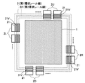
<レール配置例1>
図3に、レール配置例1を示す。
図3に図解するように、電源遮断対象の回路ブロック1の4辺に近接して、当該回路ブロック1を囲むように複数のスイッチブロック2が配置されている。ここで便宜上、スイッチブロック2を、電源遮断対象の回路ブロック1の辺ごとに、上部スイッチブロック2U、下部スイッチブロック2D、右側スイッチブロック2R、左側スイッチブロック2Lに分類する。上部スイッチブロック2U同士、下部スイッチブロック2D同士、右側スイッチブロック2R同士、左側スイッチブロック2L同士は、それぞれ同じ構成を有する。
<Rail arrangement example 1>
FIG. 3 shows an example 1 of rail arrangement.
As illustrated in FIG. 3, a plurality of switch blocks 2 are arranged so as to surround the
4種類のスイッチブロック2U,2D,2R,2Lは、それぞれ、電圧線セグメント21と、不図示のスイッチとを備える。
電圧線セグメント21は、図3に破線で示し、電源遮断対象の回路ブロック1の周囲に閉じた環状線を形成する環状レール線3の一部となる配線部分である。
配置配線の設計段階では、スイッチを配置した後の配線段階で環状レール線3がスイッチ等に対して配置接続される。一旦、配置接続された後は、スイッチブロック2U,2D,2R,2L単位で、電圧線セグメント21以外の構成要素(スイッチを含む)を移動させて、その移動後の位置で、環状レール線3へスイッチ等を接続させる。なお、この図3では、電源遮断対象の回路ブロック1内の内部電圧線11(図2参照)とスイッチの接続配線は、スイッチブロック移動のたびに変更する必要がある。ただし、環状レール線3に関しては、スイッチとの接続配線を変更する手間がなく、その分、スイッチの移動が容易である。
Each of the four types of
The
In the layout and wiring design stage, the
スイッチブロックを挿入する場合は、同様にして、スイッチブロック内の電圧線セグメント21以外の構成要素を単位として、これを必要数、必要な場所に挿入し、その場所における環状レール線3にスイッチ等を接続する。
スイッチを削除する場合も同様であり、スイッチブロック内の電圧線セグメント21以外の構成要素を単位として削除する。
スイッチの挿入、削除においても、環状レール線3に関しては、スイッチとの接続配線を変更する手間がなく、その分、スイッチの移動が容易である。
In the case of inserting a switch block, in the same manner, a component other than the
The same applies to the case of deleting the switch, and the components other than the
Even when the switch is inserted or deleted, there is no need to change the connection wiring with the switch with respect to the
<レール配置例2>
図4に、レール配置例2を示す。
図4に示す配置例が図3と異なる第1の点として、「第1環状レール線」としての環状レール線3に加えて、「第2環状レール線」としての仮想環状レール線3Vが設けられている。
仮想環状レール線3Vは、環状レール線3と電源遮断対象の回路ブロック1との間に、環状レール線3と並行に配置される。仮想環状レール線3Vは、電源遮断対象の回路ブロック1内の内部電圧線11(図2参照)に対し、所定の箇所、例えば図2の場合、内部電圧線11の各端部(ロウ方向3箇所、カラム方向4箇所)に接続されている。
スイッチブロック2U,2D,2R,2Lの各々において、環状レール線3(電圧線セグメント21)と仮想環状レール線3V(仮想電圧線セグメント21V)間に、不図示のスイッチが接続されている。
<Rail arrangement example 2>
FIG. 4 shows a second rail arrangement example.
4 is provided with a virtual
The virtual
In each of the switch blocks 2U, 2D, 2R, 2L, a switch (not shown) is connected between the annular rail line 3 (voltage line segment 21) and the virtual
第2の相違点として、スイッチブロック2U,2D,2R,2Lの各々に、「第1電圧線セグメント」としての電圧線セグメント21と並行に、「第2電圧線セグメント」としての仮想電圧線セグメント21Vを備える。
その他の、スイッチブロック2U,2D,2R,2Lの電源遮断対象の回路ブロック1に対する配置自体は、図3と共通する。
The second difference is that each of the switch blocks 2U, 2D, 2R, 2L has a virtual voltage line segment as a “second voltage line segment” in parallel with the
Other arrangements of the switch blocks 2U, 2D, 2R, and 2L with respect to the
レール配置例2においても、レール配置例1と同様に、スイッチブロックの電圧線セグメント21および仮想電圧線セグメント21Vを除く構成要素を移動、挿入、削除するだけで、環状レール線3に関しては、スイッチとの接続配線を変更する手間がなく、その分、スイッチの移動が容易である。
さらに、レール配置例2においては、仮想環状レール線3Vが、例えば内部電圧線11の各端部(ロウ方向3箇所、カラム方向4箇所)と接続されているが、この接続箇所に変更を加えることなく、仮想環状レール線3Vに関しても、スイッチとの接続配線を変更する手間がなく、その分、スイッチの移動が容易である。
In the rail arrangement example 2 as well, as in the rail arrangement example 1, only the components other than the
Further, in the rail arrangement example 2, the virtual
上述したレール配置例1(図3)およびレール配置例2(図4)において、上述したスイッチブロックの電圧線セグメント21(および仮想電圧線セグメント21V)を除く構成要素を環状レール線3(および仮想環状レール線3V)に沿って移動、挿入、削除するだけで自由にスイッチブロックの位置や数の変更が可能であることは既に述べた。
この自由な設計変更を可能とするためには、スイッチブロック2U,2D,2R,2Lのサイズが同じであり、そのブロック枠の、環状レール線3(および仮想環状レール線3V)が横切る各対向2辺において、電圧線セグメント21(および仮想電圧線セグメント21V)の端辺位置が規格化されている(一定となっている)ことが必要である。
In the rail arrangement example 1 (FIG. 3) and the rail arrangement example 2 (FIG. 4) described above, the components other than the voltage line segment 21 (and virtual
In order to enable this free design change, the sizes of the switch blocks 2U, 2D, 2R, and 2L are the same, and each block frame is opposed to each other across the annular rail line 3 (and the virtual
なお、端辺位置が規格化されていない場合、スイッチブロックの電圧線セグメント21(および仮想電圧線セグメント21V)を除く構成要素を環状レール線3(および仮想環状レール線3V)に沿って移動、挿入、削除した後に、隣り合うスイッチブロック間で端辺同士を結ぶように電圧線セグメント21(および仮想環状レール線3V)のパターンを修正する必要がある。ただし、この作業は端辺を結ぶ簡単な作業であるため自動化が可能である。よって、スイッチ配置後に、スイッチより外側に配置されている環状線と手作業で他の階層の配線層を用いて接続配線をやり直す場合に比べると、各段にスイッチ配置変更が容易である。
If the edge positions are not standardized, the components other than the voltage line segment 21 (and virtual
<スイッチ制御線>
図3および図4では図示を省略しているが、スイッチの制御線は、同時制御するスイッチ群の個数により、複数配線されることがある。
<Switch control line>
Although not shown in FIGS. 3 and 4, a plurality of switch control lines may be wired depending on the number of switch groups to be controlled simultaneously.
図5は、制御線が2本の場合における、制御線の配線例を示す図である。ここで、環状レール線については、レール配置例2(図4)が採用されている。
図5に示す制御回路34は、例えば、図1における通電回路ブロック32や非適用回路ブロック33などの、MTCMOS非適用回路ブロックに設けられることにより、当該半導体集積回路の起動後は常時、電源供給を受けて動作可能な回路である。制御回路34からの制御線35は、上部スイッチブロック2U、左側スイッチブロック2L、下部スイッチブロック2D、右側スイッチブロック2Rの順に配線され、制御信号が、この順で印加される。制御信号により、各スイッチブロック内のスイッチの導通と非導通が制御される。
FIG. 5 is a diagram illustrating an example of wiring of control lines when there are two control lines. Here, the rail arrangement example 2 (FIG. 4) is adopted for the annular rail line.
The
なお、図5に示す構成は、図6に示す環状レール線を有しない構成と置き換えて使用可能とするために、環状レール線3の所定箇所に実VSS配線の分岐が設けられている。
図6に示す、本発明が非適用の外部SW配置構成は、格子状に設けられたグローバルな各実VSS配線5を、スイッチブロックSBを介して電源遮断対象の回路ブロック1に接続させている。
図5に示す環状レール線3は、格子状配置の実VSS配線5と、ロウ方向2箇所、カラム方向4箇所で接続されている。
一方、仮想環状レール線3Vは、電源遮断対象の回路ブロック1と、ロウ方向6箇所、カラム方向8箇所で接続されている。
これらの接続箇所は、スイッチブロック2U,2D,2R,2Lを移動、挿入、削除する際に全く変更する必要がない。
Note that the configuration shown in FIG. 5 is provided with a branch of the actual VSS wiring at a predetermined position of the
In the external SW arrangement configuration to which the present invention is not applied as shown in FIG. 6, each global
The
On the other hand, the virtual
These connection points need not be changed at all when the switch blocks 2U, 2D, 2R, and 2L are moved, inserted, and deleted.
つぎに、2本の制御線35によりスイッチ制御される場合を例として、より詳細なスイッチ構成を、図面を参照して説明する。
Next, a more detailed switch configuration will be described with reference to the drawings, taking as an example the case of switch control by two
<スイッチ構成例>
図7は、基準電圧VSS(例えば0[V])が印加される電圧線セグメント21と、仮想基準電圧VSSVで保持される仮想電圧線セグメント21V間のスイッチトランジスタの配置を模式的に示す、スイッチブロックの構成図である。
図7において、電圧線セグメント21に3本の分岐線21Bが設けられており、仮想電圧線セグメント21Vに3本の分岐線21VBが設けられている。分岐線21Bと分岐線21VBは交互に配置されている。1本の分岐線21Bと、隣接する1本の分岐線21VBとの間に4個のスイッチトランジスタSWTが並列に接続されている。このスイッチトランジスタ列は5段設けられ、全体で4×5=20個のスイッチトランジスタSWTがマトリクス配置されている。
<Switch configuration example>
FIG. 7 schematically shows the arrangement of switch transistors between a
In FIG. 7, the
20個のスイッチトランジスタSWTのうち、各段1つずつ、合計5個のスイッチトランジスタSWTが、不図示の1本の制御線により導通と非導通が制御される。この5個のスイッチトランジスタSWTの回路記号部分を、図7では暗いメッシュを施して示している。メッシュが施されていない他の15個のスイッチトランジスタSWTは、他の制御線により同時制御される。 Of the 20 switch transistors SWT, conduction and non-conduction are controlled by a single control line (not shown) for a total of five switch transistors SWT, one for each stage. The circuit symbol portions of the five switch transistors SWT are shown with a dark mesh in FIG. The other 15 switch transistors SWT that are not meshed are simultaneously controlled by other control lines.
このように一部のスイッチと、他のスイッチを分けて制御するのは、電源遮断対象の回路ブロック1(図1〜図5参照)の電源供給を遮断した停止状態から、電源供給を開始して動作状態に復帰する際に、急激なスイッチングによる電圧線セグメント21(環状レール線3)の電位変動を抑制するためである。したがって、少ない個数、ここでは5個のスイッチトランジスタSWTを先にオンして、比較的高いオン抵抗である程度、仮想電圧線セグメント21V(電源遮断対象の回路ブロック1内の内部電圧線11)の電位を下げてから、安定したら、残りの15個のスイッチトランジスタSWTをオンする制御が行われる。これにより、環状レール線3から実VSS配線5に伝達する基準電圧VSSの電位上昇(電源ノイズ)のピーク値を、他の常時動作中の回路に影響がない程度に抑圧する。
In this way, some switches and other switches are controlled separately by starting the power supply from the stop state in which the power supply of the circuit block 1 (see FIGS. 1 to 5) to be powered off is cut off. This is to suppress potential fluctuation of the voltage line segment 21 (annular rail line 3) due to abrupt switching when returning to the operating state. Therefore, the potential of the virtual
図8(A)〜図9(B)に、実際のスイッチブロック内配置例を示す。ここで図3および図4との対応関係で言うと、図8(A)は上部スイッチブロック2U、図8(B)は下部スイッチブロック2D、図9(A)は左側スイッチブロック2L、図9(B)は右側スイッチブロック2Rを、それぞれ示す。
4種類のスイッチブロック2U,2D,2R,2Lは同じサイズを有する。ここで、基準電圧VSS、仮想基準電圧VSSVおよび制御信号が入出力するブロック枠の辺(以下、接続辺という)、すなわち、図8(A)の辺LU1とLU2、図8(B)の辺LD1とLD2、図9(A)の辺LL1とLL2、ならびに、図9(B)の辺LR1とLR2は、同じ長さに設定されている。また、これらの接続辺における、電圧線セグメント21、仮想電圧線セグメント21V、第1スイッチ制御線35_1、第2スイッチ制御線35_2の各端辺は、どの接続辺でも同じ位置に規格化されている。
FIG. 8A to FIG. 9B show actual arrangement examples in the switch block. 3 and FIG. 4, FIG. 8A shows the
The four types of
ここで第1スイッチ制御線35_1は、図7と同様に先に制御される数個のスイッチトランジスタSWTを制御し、第2スイッチ制御線35_2は、残りの数個のスイッチトランジスタSWTを制御するものである。 Here, the first switch control line 35_1 controls several switch transistors SWT previously controlled as in FIG. 7, and the second switch control line 35_2 controls the remaining several switch transistors SWT. It is.
図8および図9に示すスイッチブロック2U,2D,2R,2Lは、図7と異なり、破線で囲むスイッチ配置領域の上方に重ねて電圧線セグメント21および仮想電圧線セグメント21Vを並行配置している。これによりブロックの占有面積を小さくできる利点がある。ただし、図7のように、スイッチ配置領域に電圧線セグメント21および仮想電圧線セグメント21Vを重ねない配置も採用可能である。
スイッチ配置領域の上方に重ねて電圧線セグメント21および仮想電圧線セグメント21Vを並行配置する場合、限られた多層配線構造の階層数では、第1および第2スイッチ制御線35_1,35_2を、スイッチ配置領域に配置することができない。よって、本例では、電源遮断対象の回路ブロック1に対する外寄りのスイッチ配置領域の外部に、第1および第2スイッチ制御線35_1,35_2を配置している。
The switch blocks 2U, 2D, 2R, and 2L shown in FIGS. 8 and 9 are different from FIG. 7 in that the
When the
図9に示す左側スイッチブロック2Lと右側スイッチブロック2Rにおいては、図7に示すスイッチセルを、X方向(図の左右の方向)に6個、Y方向(図の上下の方向)に6個の合計36個、配置している。
これに対し、図8に示す上部スイッチブロック2Uと下部スイッチブロック2Dでは、スイッチセルの合計数は36個と図9の場合と同じであるが、X方向の配置数が12個、Y方向の配置数が3個となっている。
その理由は、スイッチセルはY方向のサイズがX方向に比べて大きいこと、ゲート電極の長手方向を図8と図9でY方向に揃える必要があることに対応して、同じサイズを有するスイッチブロック内に収容するスイッチ配置領域の縦横比を、図8と図9で入れ替わっているスイッチブロックの縦と横のサイズに適合させるためである。
In the
On the other hand, in the
The reason is that the switch cell has the same size corresponding to the fact that the size of the switch cell is larger than that of the X direction and the longitudinal direction of the gate electrode needs to be aligned in the Y direction in FIGS. This is because the aspect ratio of the switch arrangement area accommodated in the block is adapted to the vertical and horizontal sizes of the switch blocks interchanged in FIGS.
図9の場合、分岐線21Bと21VBの全てに対し、電圧線セグメント21と仮想電圧線セグメント21Vの各々が交差している。このため、電圧線セグメント21は、下層の全ての分岐線21Bと21VBにコンタクトを介して接続することができ、また、仮想電圧線セグメント21Vは、下層の全ての分岐線21Bと21VBにコンタクトを介して接続することができる。
これに対し、図8の場合、電圧線セグメント21と仮想電圧線セグメント21Vは、コンタクトをとるべき下層配線(分岐線21Bと21VB)全てに交差していはいない。よって、図8に示すように、上部スイッチブロック2Uおよび下部スイッチブロック2Dにおいては、電圧線セグメント21から分岐線21Bまでのアクセス経路に、電圧線セグメント21および分岐線21Bと直交するアクセス分岐線21Baを設ける必要がある。アクセス分岐線21Baは、電圧線セグメント21より下層で、分岐線21Bより上層の配線層から形成される。よって、電圧線セグメント21の分岐線がアクセス分岐線21Baであり、さらに、アクセス分岐線21Baから分岐線21Bが分岐する2段階分岐構造が採用されている。
同様に、仮想電圧線セグメント21Vから、これと直交するアクセス分岐線21VBaが分岐し、さらにアクセス分岐線21VBaから、これと直交する分岐線21VBが分岐することによって、2段階分岐構造が採用されている。
In the case of FIG. 9, each of the
On the other hand, in the case of FIG. 8, the
Similarly, an access branch line 21VBa that is orthogonal to the virtual
第1スイッチ制御線35_1が制御する数個のスイッチトランジスタSWTの総ゲート幅(長手方向のトータルの長さ)が、図8と図9では同じに設定されている。同様に、第2スイッチ制御線35_2が制御する残りの数個のスイッチトランジスタSWTについても、その総ゲート幅が図8と図9では同じに設定されている。 The total gate width (total length in the longitudinal direction) of several switch transistors SWT controlled by the first switch control line 35_1 is set to be the same in FIGS. Similarly, the total gate widths of the remaining several switch transistors SWT controlled by the second switch control line 35_2 are set to be the same in FIGS.
スイッチブロック2U,2D,2R,2Lの各々は、スイッチ配置領域の回路ブロック1と反対の側(外側)に、第1スイッチ制御線35_1の途中に設けられているバッファ回路BUF1と、第2スイッチ制御線35_2の途中に設けられているバッファ回路BUF2とを備える。
バッファ回路BUF1,BUF2は、不図示の実VDD線と電圧線セグメント21に接続されることにより、伝送途中で減衰した制御信号を電源電圧VDD振幅のパルス信号に波形整形する役目がある。このため、破線により示すバッファ回路の配置領域はスイッチ配置領域より外側に設けられている。
Each of the switch blocks 2U, 2D, 2R, 2L includes a buffer circuit BUF1 provided in the middle of the first switch control line 35_1 on the side (outside) opposite to the
The buffer circuits BUF1 and BUF2 are connected to a real VDD line and a voltage line segment 21 (not shown), thereby having a function of shaping a control signal attenuated during transmission into a pulse signal having a power supply voltage VDD amplitude. For this reason, the arrangement area of the buffer circuit indicated by the broken line is provided outside the switch arrangement area.
バッファ回路BUF1,BUF2の各出力からは、スイッチ制御のための配線がそれぞれスイッチ配置領域に延び、対応するスイッチトランジスタ群のゲートに接続されている。
なお、この配線、ならびに、第1スイッチ制御線35_1および第2スイッチ制御線35_2は、図8および図9ではラインで示しているが、実際には、電圧線セグメント21等と同様な幅を有する配線層で形成されている。
第1スイッチ制御線35_1および第2スイッチ制御線35_2は、それぞれ、スイッチブロック内において、対応するバッファ回路BUF1,BUF2の入力側に設けられ、制御信号が入力される「第1制御線セグメント」と、出力側に設けられ、波形整形された制御信号が出力される「第2制御線セグメント」を有して構成されている。
From each output of the buffer circuits BUF1 and BUF2, wiring for switch control extends to the switch arrangement region and is connected to the gate of the corresponding switch transistor group.
In addition, although this wiring and the 1st switch control line 35_1 and the 2nd switch control line 35_2 are shown by the line in FIG.8 and FIG.9, actually, it has the width | variety similar to the
The first switch control line 35_1 and the second switch control line 35_2 are provided on the input side of the corresponding buffer circuits BUF1 and BUF2 in the switch block, respectively, and are “first control line segments” to which control signals are input. The “second control line segment” is provided on the output side and outputs a waveform-shaped control signal.
<配線構造>
図10に、多層配線構造における各階層の配線層の使用例を示す。ここでは、多層配線構造において、下層から順に積層された第1階層の配線層(第1配線層(1M))〜第7階層の配線層(第7配線層(7M))を利用して、各配線を形成している。
<Wiring structure>
FIG. 10 shows an example of use of wiring layers at each level in a multilayer wiring structure. Here, in the multilayer wiring structure, using the first layer wiring layer (first wiring layer (1M)) to the seventh layer wiring layer (seventh wiring layer (7M)) stacked in order from the lower layer, Each wiring is formed.
具体的には、電源遮断対象の回路ブロック1内のインバータセル13(図2)等の標準セル15間を第1配線層(1M)〜第4配線層(4M)から形成している。また、ある標準セル15から外部へ引き出す信号線も、第1配線層(1M)〜第4配線層(4M)で形成している。
Specifically, the
環状レール線3のカラム方向の配線3Cを、第5配線層(5M)から形成している。環状レール線3のロウ方向の配線3Rを、カラム方向の配線3Cの両端に接続された1階層上の第6配線層(6M)により形成している。
同様に、仮想環状レール線3Vのカラム方向の配線3VCを、第5配線層(5M)から形成している。仮想環状レール線3Vのロウ方向の配線3VRを、カラム方向の配線3VCの両端に接続された1階層上の第6配線層(6M)により形成している。
The
Similarly, the wiring 3VC in the column direction of the virtual
一方、内部電圧線11のロウ方向の配線11Rは、第5配線層(5M)により形成された仮想環状レール線3Vのカラム方向の配線3VCに接続するために、それより1階層上の第6配線層(6M)により形成している。さらに、6Mにより形成された当該内部電圧線11のロウ方向の配線11Rは、それよりさらに1階層上の第7配線層(7M)により形成された、内部電圧線11のカラム方向の配線11Cと、交差箇所で接続されている。
なお、実VSS配線5も第7配線層(7M)により形成されている。
On the other hand, the
The
このように、カラム方向の配線を、ロウ方向の1階層下の配線から形成し、そのルールを適用しながら配線間接続を上手に達成している。 In this way, the wiring in the column direction is formed from the wiring one layer below in the row direction, and the interwiring connection is successfully achieved while applying the rule.
以上の説明では、スイッチセルのパターンについては任意であり言及しなかったが、次に、望ましい具体例として、2軸対称パターンを有するスイッチセルについて説明する。
図11に、1つのスイッチセルの概略的なレイアウト図を示す。なお、図11は、パターンの寸法等が実際のものと等しい訳ではなく、パターンの大まかな配置と接続関係を模式的に示すに過ぎない。
In the above description, the switch cell pattern is arbitrary and not mentioned. Next, a switch cell having a biaxial symmetry pattern will be described as a desirable specific example.
FIG. 11 shows a schematic layout diagram of one switch cell. In addition, FIG. 11 does not necessarily mean that the dimension of the pattern is the same as the actual one, but merely schematically shows the rough arrangement of the pattern and the connection relationship.
図11に示すスイッチセル20Nは、1つのNMOSトランジスタをスタンダードセル化したものであり、セル中心を通るX軸とY軸それぞれに対し、軸対称な配置となっている。以下、この対称性を「2軸対称」という。
A
図11に図解するスイッチセル20Nの全領域がPウェルの一部となっている。
X軸に沿ってセル中心を通るゲート電極の連結部21Cが形成されている。連結部21Cのセル中心からの長さは、Y軸を境に同じ(対称)である。つまり、連結部21Cは2軸対称のパターンを有する。
連結部21Cから、その幅方向の一方側に同じ長さの4本のゲート電極21Aが延び、他方側に同じ長さの4本のゲート電極21Bが延びている。4本のゲート電極21Aは、X軸方向において等間隔に配置され、4本のゲート電極21Bは、同様にX軸方向において等間隔に配置され、全て同じ長さと太さを有するためY軸対称となっている。ゲート電極21Aと21Bは、連結部21Cからの分岐箇所が同じであるため、X軸対称となっている。連結部21C、ゲート電極21Aと21Bは、同じ導電材料を加工して一体として形成されている。
The entire region of the
A gate electrode connecting portion 21C passing through the center of the cell along the X axis is formed. The length of the connecting portion 21C from the cell center is the same (symmetric) with respect to the Y axis. That is, the connecting portion 21C has a biaxially symmetric pattern.
From the connecting portion 21C, four
X軸から等距離で、同じサイズの2つのN型活性領域22Aと22Bが、Pウェルに形成されている。N型活性領域22Aは4本の4ゲート電極21Aに交差する位置に形成され、N型活性領域22Bは4本のゲート電極21Bに交差する位置に形成されている。N型活性領域22Aと22Bは、ゲート電極21Aと21Bを形成後に、これらのゲート電極をマスクとしてN型不純物を選択的にPウェルに導入することにより形成される。
N型活性領域22Aと22Bは、それぞれ、ゲート電極部分で分断され、交互にソース(S)とドレイン(D)として機能する5つの領域から構成されている。
これにより、N型活性領域22Aの分離部分をチャネルとする第1単位トランジスタ(TR1)と、N型活性領域22Bの分離部分をチャネルとする第2単位トランジスタ(TR2)の、2軸対称性を有する基本構造が形成されている。
Two N-type
Each of the N-type
Thus, the biaxial symmetry of the first unit transistor (TR1) having the isolation portion of the N-type
第1単位トランジスタ(TR1)の配置領域において、第2配線層(2M)から形成されている電圧セル線23Aが、4本のゲート電極21Aと直交して配置されている。同様に、第2単位トランジスタ(TR2)の配置領域において、第2配線層(2M)から形成されている電圧セル線23Bが、4本のゲート電極21Bと直交して配置されている。
2本の電圧セル線23Aと23Bは、それぞれ、より上層の仮想電圧線セグメント21V(図7参照)によって、回路ブロック1内の内部電圧線11(図2参照)と、電気的に接続されるセル内部線である。つまり、図7との対応関係で言うと、図11の2本の電圧セル線23Aと23Bが、図7の1本の分岐線21VBに対応する。
In the arrangement region of the first unit transistor (TR1), the
The two
N型活性領域22Aと22Bの夫々において、2つのドレイン(D)の各々に対し1stコンタクト(1C)を介して接続する、2つのドレイン線28が設けられている。N型活性領域22Aと22Bで2つずつ、合計4つのドレイン線28は、第1配線層(1M)により形成されている。
N型活性領域22A上の2つのドレイン線28に、2ndコンタクト(2C)を介して電圧セル線23Aが接続されている。同様に、N型活性領域22B上の2つのドレイン線28に、2ndコンタクト(2C)を介して電圧セル線23Bが接続されている。
2本の電圧セル線23Aと23Bは、互いに平行で、かつ、X軸から等距離に配置されている。
In each of the N-type
The
The two
4本のゲート電極21Aの先端側に、電圧セル線23Aと平行な電源セル線24Aが配置されている。同様に、4本のゲート電極21Bの先端側に、電圧セル線23Bと平行な電源セル線24Bが配置されている。
2本の電源セル線24Aと24Bは、それぞれ、より上層の実VDD線(図7の電圧線セグメント21)と、電気的に接続されるセル内部線である。つまり、このため、2本の電源セル線24Aと24Bは、図7との対応関係で言うと、図11の2本の電源セル線24Aと24Bが、図7の1本の分岐線21Bに対応する。
A
The two
2本の電源セル線24Aと24Bは、それぞれ、不図示のP型活性領域等と同時形成される配線領域24dと、第1配線層(1M)から形成されている第1裏打配線24m1と、第2配線層(2M)から形成されている第2裏打配線24m2とを含んで構成されている。
2本の電源セル線24Aと24Bの夫々において、配線領域24dと第1裏打配線24m1は1stコンタクト(1C)により等間隔で短絡され、第1裏打配線24m1と第2裏打配線24m2は2ndコンタクト(2C)により等間隔で短絡されている。
電源セル線24Aを構成する第1裏打配線24m1は、N型活性領域22Aの2つのソース(S)側に延びる、2本のソース線24Sと一体に形成されている。同様に、電源セル線24Bを構成する第1裏打配線24m1は、N型活性領域22Bの2つのソース(S)側に延びる、2本のソース線24Sと一体に形成されている。
そして、各ソース(S)が、ソース線24Sと1stコンタクト(1C)を介して接続されている。
The two
In each of the two
The first backing wiring 24m1 constituting the
Each source (S) is connected to the
ここで、最初に説明したゲート電極の連結部21Cは省略可能で、4つのコンタクトパッド部で代替可能である。
何れの場合でも、全体として、Y軸と平行なゲート電極21Aと21Bからなる4本のゲート電極が、それより上層の配線層で短絡されている。このゲート電極を短絡するセル内部配線を「制御セル線」と称する。
本例の制御セル線25は、第1配線層(1M)からなる第1制御セル線26と、第2配線層(2M)からなる第2制御セル線27を重ねて形成されている。連結部21C(または4つのコンタクトパッド部)と第1制御セル線26が1stコンタクト(1C)により接続され、第1制御セル線26と第2制御セル線27が2ndコンタクト(2C)により接続されている。
制御セル線25が、その幅方向と長さ方向の中心をセル中心に一致させて、X軸に沿って配置されている。
よって、制御セル線25は、2本の電圧セル線23Aと23B、2本の電源セル線24Aと24Bの夫々に対し並行配置されている。
Here, the gate electrode connecting portion 21C described first can be omitted, and can be replaced by four contact pad portions.
In any case, as a whole, the four gate electrodes composed of the
The
The
Therefore, the
図12に、PMOSトランジスタのスイッチセル20Pを示す。
図12に図解するスイッチセル20Pが、図11のスイッチセル20Nと異なる点は、全体がNウェルに形成され、Nウェルに形成されている第1単位トランジスタ(TR1)と第2単位トランジスタ(TR2)の活性領域が、P型のN型活性領域22APと22BPであることである。その他の構成は、図5と同じであるため、同一符号を付して、説明を省略する。
FIG. 12 shows a
The
図13(A)と図13(B)に、図12のNMOSトランジスタ構成のスイッチセル20Nを利用する、上部スイッチブロック2Uと下部スイッチブロック2Dの構成図を示す。また、図14(A)と図14(B)に、同様にスイッチセル20Nを利用する、左側スイッチブロック2Lと右側スイッチブロック2Rの構成図を示す。
図13および図14を、図8および図9と比較すると、図8および図9の分岐線21Bに対応する電源セル線24ABが、分岐線21Bの2倍の密度で形成され、図8および図9の分岐線21Bに対応する電圧セル線23Aと23Bが、分岐線21VBの2倍の密度で形成されていることが分かる。ここで電源セル線24ABは、図11における電源セル線24Aと、Y方向に隣接する他のセルの電源セル線24Bと共有させたものである。
他の構成は共通するため、ここでの説明を省略する。
FIGS. 13A and 13B are configuration diagrams of the
Comparing FIG. 13 and FIG. 14 with FIG. 8 and FIG. 9, the power cell line 24AB corresponding to the
Since other configurations are common, description thereof is omitted here.
図13および図14では図示を省略しているが、第1および第2スイッチ制御線35_1,35_2の各々に対し、所定の数で、所定の位置のスイッチセル20Nを接続するためにも、多層配線構造が利用される。配線層を多層化すれば、スイッチ制御線のブロック中心に対する対称配置も可能であるが、このためだけに配線構造を複雑化して製造コストを上げるのは望ましくない。また、本例ではバッファ回路BUF1,BUF2を配置する必要から、スイッチブロックの中心に対し、第1および第2スイッチ制御線35_1,35_2を非対称配置せざるを得ない。
Although not shown in FIGS. 13 and 14, in order to connect the
つぎに、このようにスイッチ制御線をブロック中心に対称配置できない場合における、スイッチセルの配線対称構造の利点を述べる。 Next, advantages of the switch cell wiring symmetrical structure when the switch control lines cannot be symmetrically arranged at the block center will be described.
第1の利点として、スイッチブロックの設計が容易であることを説明する。
本実施形態で好ましいスイッチの配置配線方法(スイッチブロック設計手法)は、スイッチセル20Nのレイアウト対称性を利用し、以下の手順をとる。
第1ステップ:トランジスタを配置し、内部電圧線11とそれぞれが電気的に接続される2本の電圧セル線23A,23Bと、電源電圧VDD(スイッチセル20Pの場合)または基準電圧VSS(スイッチセル20Nの場合)が印加される第2電源線に対しそれぞれが電気的に接続される2本の電源セル線24A,24B(または、2本の共有された電源セル線24AB)と、スイッチ制御線29A〜29Cに対し電気的に接続される制御セル線25との各々を、セル中心を通るX軸およびY軸それぞれに対して軸対称に配置し、かつ、トランジスタに対し接続することにより、スイッチセル20Nあるいは20P(またはその両方)を形成する。
第2ステップ:形成されたスイッチセル20Nあるいは20P(またはその両方)を行列状に配置し、複数のスイッチ制御線29A〜29Cの各々に対し、所定のスイッチセル20Nあるいは20P(またはその両方)を接続してスイッチブロック20を形成する。
第3ステップ:スイッチブロック2の作成済みデータを、X軸またはY軸と平行なラインを軸としてミラー反転し、または、セル中心を軸として180度回転(180度反転)することにより、反転スイッチブロックを形成する。
第4ステップ:配置されたスイッチブロックおよび反転スイッチブロック間で複数のスイッチ制御線29A〜29Cおよび第2電源線を接続し、電圧セル線23A,23Bを回路ブロック1の内部電圧線11と接続する。
The first advantage will be described that the design of the switch block is easy.
A preferred switch placement and routing method (switch block design method) in the present embodiment uses the layout symmetry of the
First step: Two
Second step: The formed
Third step: Reversing switch by mirror-inverting the created data of
Fourth step: A plurality of switch control lines 29A to 29C and a second power supply line are connected between the arranged switch block and inverting switch block, and the
重複するが、より具体的に説明すると、制御セル線25、電圧セル線23Aと23B、および、電源セル線24Aと24B(または、2つの電源セル線24AB)が、X軸とY軸のそれぞれに対して対称である。このため、スイッチセル20NをX軸またはY軸に沿ったラインを反転軸としてミラー反転し、あるいは、セル中心を軸として180度回転しても、上記5本のセル線の位置関係は元のままである。
とくにトランジスタまで2軸対称配置されている図5の場合は、あるスイッチブロック2を、例えば図4のようにスイッチ制御線まで設計した段階で、ブロックごとミラー反転または180度回転しても、行列状のスイッチセル群において、図11に示す、各スイッチセル20Nの基本パターンに何ら変化はない。変化があるのは、ブロック内で対称配置されていない、第3配線層(3M)以上の配線層により形成された、スイッチ制御線29A〜29Cとその接続線である。
More specifically, the
In particular, in the case of FIG. 5 in which two transistors are symmetrically arranged up to the transistor, even if a
回路ブロック1から第1および第2スイッチ制御線35_1,35_2の各々の距離が同じであると、ブロック間配線が容易である。また、トランジスタのゲートの向き(長手方向)は、特性を揃えるため集積回路内で同じとする制約があることが多い。このような場合、回路ブロック1の4辺に配置するスイッチブロックは、辺ごとに異なるパターンとなる。
しかしながら、図11に示すような、5本のセル線、即ち電圧セル線23Aと23B、電源セル線24Aと24B、および、制御セル線25が2軸対称性を有するスイッチセルを用いると、前述した第1〜第5ステップの手順を有する方法によって、簡単にスイッチブロックの設計が可能になる。
When the distances from the
However, if the five cell lines, that is, the
この5本のセル線の関係が、ミラー反転または180度回転の前後で変化せず、それより上層の配線が変化することを利用すると、第1および第2ステップで、回路ブロック1の対向する2辺のうち、一方の辺側に配置すべき1つのスイッチブロック2を設計後に、設計後のスイッチブロック2のデータを、上記2辺と平行なラインを軸としてミラー反転する、あるいは、180度回転することにより、他の辺側に配置すべきもう片方のスイッチブロック2のデータを、容易に作成できる(第3ステップ)。
同様にして、他の2辺においても、その1つの辺側に配置すべきスイッチブロック2を第1および第2ステップで設計後に、設計後のデータをミラー反転または180度回転することにより(第3ステップ)、他の1つの辺側に配置すべきスイッチブロック2のデータを容易に作成できる。
このようにして作成された4種類のスイッチブロック(2U,2D,2L,2R)は、それらのスイッチ制御線29A〜29Cそれぞれの、回路ブロック1までの距離が、4種類のスイッチブロックで同じであるため、第4ステップにおけるスイッチ制御線のブロック間接続が容易である。また、このことは、スイッチブロック間接続すべき他の配線についても言える。
If the relationship between the five cell lines does not change before and after mirror inversion or 180 ° rotation, and the fact that the wiring in the upper layer changes, the
Similarly, on the other two sides, after designing the
The four types of switch blocks (2U, 2D, 2L, 2R) created in this way have the same distance from the switch control lines 29A to 29C to the
次に、第2の利点として、スイッチセルの設計自体が容易であることを説明する。
5本のセル線の対称性に加え、図11や図12のように、トランジスタのパターンまで2軸対称であると、X軸とY軸で区画される第1〜第4象限のパターン(以下、4分割パターンという)は、その1つの4分割パターンを設計し、後は、設計後のパターンデータをコピーし、ミラー反転、あるいは、ミラー反転と180度回転を組み合わせながらペーストするだけで、残りの3つの4分割パターンが形成され、スイッチセルの設計が完結する。
よって、スイッチセルの設計が非常に容易である。また、4分割パターンを最初に設計する段階で、最大限のゲート幅が確保できるように高密度設計すると、無駄がないスイッチセルの設計ができる。
Next, as a second advantage, the fact that the switch cell design itself is easy will be described.
In addition to the symmetry of the five cell lines, as shown in FIG. 11 and FIG. 12, if the transistor pattern is biaxially symmetric, the pattern in the first to fourth quadrants divided by the X axis and the Y axis (hereinafter referred to as the pattern) 4 pattern) is designed, and after that, the pattern data after the design is copied and pasted by mirror inversion or by combining mirror inversion and 180 degree rotation. Thus, the design of the switch cell is completed.
Therefore, the design of the switch cell is very easy. In addition, if the high-density design is performed so that the maximum gate width can be ensured at the stage of designing the quadrant pattern first, a switch cell can be designed without waste.
本実施形態によれば、以下の利益が得られる。
電源遮断対象の回路ブロック1の周囲に複数配置されるスイッチブロックが、電源電圧または基準電圧が印加される環状レール線の一部となる電圧線セグメントとスイッチを備える。このため、当該電圧線セグメントとスイッチ間の位置関係が固定された状態でスイッチブロックを移動、挿入、削除するだけで、あたかも、環状線レールに沿ってスイッチセグメントを自由に移動し、新たに挿入し、あるいは削除することが容易に行える。
According to this embodiment, the following benefits can be obtained.
A plurality of switch blocks arranged around the
特に、図15に示すように、電源遮断対象の回路ブロック1の4辺の各辺からみた、当該回路ブロック1への電源電圧または基準電圧を供給する配線(本実施形態の説明においては、具体的には実VSS配線5および環状レール線3)の配線のインピーダンスが小さいほどスイッチブロック数を増やすように、複数のスイッチブロックが配置されている。
図15では、太い矢印で示す側のインピーダンスが、細い矢印で示す側より低い。つまり、太い矢印の側には図1に示す入出力セル40が配置されているため、外部からの基準電圧が0[V]にほぼ近い値をとる。これに対し、細い矢印で示す側には常時動作する他の回路ブロック(例えば通電回路ブロック32)が配置されているため、実VDD線の電位が、時間平均をとると0[V]より高い状態となる。
In particular, as shown in FIG. 15, a wiring for supplying a power supply voltage or a reference voltage to the
In FIG. 15, the impedance indicated by the thick arrow is lower than that indicated by the thin arrow. That is, since the input /
このような場合、スイッチブロックを基準電圧が0[V]に固定されている側で多く配置すると、同じスイッチオンの時間内に、より効率的に内部電圧線11の放電が進む。これとは逆に、基準電圧が0[V]より高い側にスイッチを多く配置すると、同じ放電効果を得るにはスイッチブロック数を多くしなければならないため、無駄が多い。
In such a case, if many switch blocks are arranged on the side where the reference voltage is fixed to 0 [V], the discharge of the
本実施形態では、このような効果的なスイッチブロックの配置が容易に行えるという効果がある。
具体的には、設計の後半での消費電力確定時での対応ができ、従来よりも使用するスイッチブロック数を削減できる。スイッチブロック数を減らして、スイッチトランジスタの総ゲート幅を削減すると、リーク電流が、その分減り、電力削減効果がある。また、入出力セル40側は動作している回路ブロックが存在しないため、放電による電源ノイズの影響が小さく、他の回路ブロックへの動作スピードへの悪影響を抑えることができる。
また、電源電圧や基準電圧が印加される環状線を、スイッチと重ねて配置できるため、面積削減効果も大きい。
In the present embodiment, there is an effect that such an effective switch block arrangement can be easily performed.
Specifically, it is possible to cope with the determination of power consumption in the second half of the design, and the number of switch blocks to be used can be reduced as compared with the conventional case. If the number of switch blocks is reduced to reduce the total gate width of the switch transistors, the leakage current is reduced by that amount, and the power is reduced. Further, since no circuit block is operating on the input /
In addition, since the annular line to which the power supply voltage and the reference voltage are applied can be placed overlapping the switch, the area reduction effect is also great.
また、2軸対称パターンを有するスイッチセルを用いた場合に、前述した第1の利点(スイッチブロックの設計が容易)と第2の利点(スイッチセルの設計自体が容易)が得られる。 Further, when a switch cell having a biaxial symmetry pattern is used, the above-described first advantage (easy to design the switch block) and second advantage (easy to design the switch cell itself) can be obtained.
1…電源遮断対象の回路ブロック、2…スイッチブロック、2U…上部スイッチブロック、2D…下部スイッチブロック、2L…左側スイッチブロック、2R…右側スイッチブロック、3…環状レール線、3V…仮想環状レール線、5…実VSS配線、11…内部電圧線、21…電圧線セグメント、21A,21B…ゲート電極、21C…連結部、21V…仮想電圧線セグメント、22A,22B…N型活性領域、22AP,22BP…、P型活性領域、23A,23B…電圧セル線、24A,24B…電源セル線、24S…ソース線、25…制御セル線、28…ドレイン線、34…制御回路、35…制御線、35_1…第1スイッチ制御線、35_2…第2スイッチ制御線、BUF1,BUF2…バッファ回路、SWT…スイッチトランジスタ
DESCRIPTION OF
Claims (13)
前記回路ブロックの周囲で閉じた環状線を形成し、電源電圧または基準電圧が印加される第1環状線と、
前記第1環状線と前記回路ブロックとの間で閉じた環状線を形成し、複数の箇所で前記複数の内部電圧線と電気的に接続されている第2環状線と、
前記回路ブロックの周囲に配置され、それぞれが矩形の外形を備える複数のスイッチブロックと、
を有し、
各スイッチブロックが、当該スイッチブロック内で互いに並行な前記第1環状線と前記第2環状線との間に電気的に接続された複数のスイッチトランジスタを備え、
前記複数のスイッチトランジスタの一部が、前記各スイッチブロック内において前記第1環状線と前記第2環状線の下層領域に配置され、
前記各スイッチブロックの外周の4辺のうち前記回路ブロックに近い内側辺から前記第1環状線までの距離が前記複数のスイッチブロックで等しく、かつ、前記内側辺から前記第2環状線までの距離が前記複数のスイッチブロックで等しい、
半導体集積回路。 A circuit block comprising a plurality of internal voltage lines arranged in a grid pattern ;
Forming a closed annular line around the circuit block, a first annular line to which a power supply voltage or a reference voltage is applied;
A second annular line that forms a closed annular line between the first annular line and the circuit block and is electrically connected to the plurality of internal voltage lines at a plurality of locations ;
A plurality of switch blocks arranged around the circuit block, each having a rectangular outer shape;
I have a,
Each switch block includes a plurality of switch transistors electrically connected between the first annular line and the second annular line parallel to each other in the switch block;
A part of the plurality of switch transistors is disposed in a lower layer region of the first annular line and the second annular line in each switch block,
The distance from the inner side close to the circuit block to the first annular line among the four sides of the outer periphery of each switch block is equal in the plurality of switch blocks, and the distance from the inner side to the second annular line Is equal in the plurality of switch blocks,
Semiconductor integrated circuit.
請求項1に記載の半導体集積回路。 The plurality of switch blocks have the same size and have at least four types of switch blocks that are different for each side of the circuit block .
The semiconductor integrated circuit according to claim 1 .
前記各スイッチブロックのブロック枠の対向する2辺における、前記2つの電圧線セグメントの端辺の位置関係が、前記複数のスイッチブロックで同じに設定されている、
請求項2に記載の半導体集積回路。 The Oite Each switch block, the first is a switch block portion of the annular beam and the second annular line two voltage line segments and the plurality of switching transistors are connected internally,
Wherein the two opposite sides of the block frame of each switch block, the positional relationship of the two end sides of the voltage line segment is set the same on the plurality of switch blocks,
The semiconductor integrated circuit according to claim 2 .
前記対向する2辺の側に配置された前記スイッチブロックが、ミラー対称または180度回転対称のパターンを有する、
請求項1から3の何れか一項に記載の半導体集積回路。 The circuit block includes an outer periphery including at least two sets of two opposite sides,
The switch blocks arranged on the two opposite sides have a mirror-symmetrical pattern or a 180-degree rotationally symmetric pattern ,
The semiconductor integrated circuit according to claim 1 .
少なくとも1組の前記対向する2辺において、一方の辺側と他方の辺側で前記スイッチブロックの配置数が異なる、
請求項1から3の何れか一項に記載の半導体集積回路。 The circuit block includes an outer periphery including at least two sets of two opposite sides,
In at least one set of the two opposing sides , the number of switch blocks arranged on one side and the other side is different .
The semiconductor integrated circuit according to claim 1 .
請求項5に記載の半導体集積回路。 Seen from each side of the outer periphery of the front Symbol circuit block, so that the impedance of the wiring for supplying a power supply voltage or reference voltage to the circuit block is a number smaller, the arrangement number of the switch blocks determined for each side of said circuit blocks It has been,
The semiconductor integrated circuit according to claim 5 .
請求項1から3の何れか一項に記載の半導体集積回路。 Within the plurality of switch blocks, the switch transistors are arranged such that the longitudinal directions of the gate electrodes are aligned in the same direction .
The semiconductor integrated circuit according to claim 1 .
請求項1から3の何れか一項に記載の半導体集積回路。 Having a plurality of switch control lines, each control different switching transistors within the switch block,
The semiconductor integrated circuit according to claim 1 .
請求項8に記載の半導体集積回路。 A buffer circuit is connected to each of the plurality of switch control lines .
The semiconductor integrated circuit according to claim 8 .
請求項9に記載の半導体集積回路。 A plurality of the buffer circuits are disposed on a side opposite to the circuit block with respect to the second annular line ;
The semiconductor integrated circuit according to claim 9 .
前記複数のスイッチトランジスタの配置領域と交差または近接して、前記第1環状線および第2環状線のスイッチブロック内部分である2つの電圧線セグメントが配置され、
前記複数のスイッチトランジスタの配置領域および前記2つの電圧線セグメントに対し前記回路ブロックと反対の側に、前記第1環状線の電圧線セグメントから電圧供給を受けて動作する前記バッファ回路が配置され、
前記バッファ回路の入力側に、制御線を介して制御信号が入力される第1制御線セグメントが配置され、
前記バッファ回路の出力側に、前記スイッチトランジスタの制御ノードに電気的に接続される第2制御線セグメントが配置されている、
請求項10に記載の半導体集積回路。 Oite said to each switch block,
Two voltage line segments that are portions in the switch block of the first annular line and the second annular line are arranged to intersect or be close to the arrangement region of the plurality of switch transistors ,
The opposite side of the circuit block to placement region and the two voltage line segment of the plurality of switch transistors, the buffer circuit which operates by receiving a voltage supply from the voltage line segment of said first annular line is arranged,
A first control line segment to which a control signal is input via a control line is disposed on the input side of the buffer circuit,
A second control line segment electrically connected to a control node of the switch transistor is disposed on an output side of the buffer circuit ;
The semiconductor integrated circuit according to claim 10 .
請求項1から3の何れか一項に記載の半導体集積回路。 The plurality of grid-like internal voltage lines are formed of wiring layers of different layers in a first direction internal voltage line and a second direction internal voltage line orthogonal to the first direction .
The semiconductor integrated circuit according to claim 1 .
請求項12に記載の半導体集積回路。 The second annular line is formed of a wiring layer in a first direction and a wiring layer in a second direction that is wired in a second direction orthogonal to the first direction and is different from the wiring layer in the first direction. Yes ,
The semiconductor integrated circuit according to claim 12 .
Priority Applications (11)
| Application Number | Priority Date | Filing Date | Title |
|---|---|---|---|
| JP2007241517A JP5528662B2 (en) | 2007-09-18 | 2007-09-18 | Semiconductor integrated circuit |
| US12/230,098 US7940080B2 (en) | 2007-09-18 | 2008-08-22 | Semiconductor integrated circuit |
| TW097134560A TWI430398B (en) | 2007-09-18 | 2008-09-09 | Semiconductor integrated circuit |
| CN201110068579.1A CN102157521B (en) | 2007-09-18 | 2008-09-18 | Semiconductor integrated circuit |
| CN2008101494840A CN101393910B (en) | 2007-09-18 | 2008-09-18 | Semiconductor integrated circuit |
| US12/929,180 US8143914B2 (en) | 2007-09-18 | 2011-01-06 | Semiconductor integrated circuit |
| US13/371,994 US8890568B2 (en) | 2007-09-18 | 2012-02-13 | Semiconductor integrated circuit |
| US14/263,598 US9058979B2 (en) | 2007-09-18 | 2014-04-28 | Semiconductor integrated circuit having a switch, an electrically-conductive electrode line and an electrically-conductive virtual line |
| US14/665,662 US9252763B2 (en) | 2007-09-18 | 2015-03-23 | Semiconductor integrated circuit having a switch, an electrically- conductive electrode line and an electrically-conductive virtual line |
| US14/956,250 US9735775B2 (en) | 2007-09-18 | 2015-12-01 | Semiconductor integrated circuit having a switch, an electrically- conductive electrode line and an electrically-conductive virtual line |
| US15/664,393 US10263617B2 (en) | 2007-09-18 | 2017-07-31 | Semiconductor integrated circuit having a switch, an electrically-conductive electrode line and an electrically-conductive virtual line |
Applications Claiming Priority (1)
| Application Number | Priority Date | Filing Date | Title |
|---|---|---|---|
| JP2007241517A JP5528662B2 (en) | 2007-09-18 | 2007-09-18 | Semiconductor integrated circuit |
Related Child Applications (1)
| Application Number | Title | Priority Date | Filing Date |
|---|---|---|---|
| JP2013029163A Division JP5549752B2 (en) | 2013-02-18 | 2013-02-18 | Semiconductor integrated circuit |
Publications (3)
| Publication Number | Publication Date |
|---|---|
| JP2009076501A JP2009076501A (en) | 2009-04-09 |
| JP2009076501A5 JP2009076501A5 (en) | 2010-11-18 |
| JP5528662B2 true JP5528662B2 (en) | 2014-06-25 |
Family
ID=40453812
Family Applications (1)
| Application Number | Title | Priority Date | Filing Date |
|---|---|---|---|
| JP2007241517A Active JP5528662B2 (en) | 2007-09-18 | 2007-09-18 | Semiconductor integrated circuit |
Country Status (4)
| Country | Link |
|---|---|
| US (7) | US7940080B2 (en) |
| JP (1) | JP5528662B2 (en) |
| CN (2) | CN101393910B (en) |
| TW (1) | TWI430398B (en) |
Families Citing this family (20)
| Publication number | Priority date | Publication date | Assignee | Title |
|---|---|---|---|---|
| JP5528662B2 (en) * | 2007-09-18 | 2014-06-25 | ソニー株式会社 | Semiconductor integrated circuit |
| US8495547B2 (en) * | 2009-11-11 | 2013-07-23 | International Business Machines Corporation | Providing secondary power pins in integrated circuit design |
| JP5404678B2 (en) * | 2011-03-10 | 2014-02-05 | 株式会社東芝 | Power control device |
| US8451026B2 (en) * | 2011-05-13 | 2013-05-28 | Arm Limited | Integrated circuit, method of generating a layout of an integrated circuit using standard cells, and a standard cell library providing such standard cells |
| US8902625B2 (en) * | 2011-11-22 | 2014-12-02 | Marvell World Trade Ltd. | Layouts for memory and logic circuits in a system-on-chip |
| US8823399B1 (en) | 2013-10-07 | 2014-09-02 | Cypress Semiconductor Corporation | Detect and differentiate touches from different size conductive objects on a capacitive button |
| JP6264860B2 (en) | 2013-11-27 | 2018-01-24 | セイコーエプソン株式会社 | Recording device |
| US9305898B2 (en) | 2014-01-23 | 2016-04-05 | Freescale Semiconductor, Inc. | Semiconductor device with combined power and ground ring structure |
| US9177834B2 (en) | 2014-02-19 | 2015-11-03 | Freescale Semiconductor, Inc. | Power bar design for lead frame-based packages |
| CN109155284B (en) * | 2016-06-01 | 2022-09-23 | 株式会社索思未来 | Semiconductor integrated circuit device having a plurality of semiconductor chips |
| KR102630392B1 (en) | 2016-12-06 | 2024-01-29 | 삼성전자주식회사 | Semiconductor device, method of designing a layout of a semiconductor device, and method of manufacturing a semiconductor device |
| US10417371B2 (en) * | 2017-01-27 | 2019-09-17 | Arm Limited | Power grid healing techniques |
| US10452803B2 (en) * | 2017-01-27 | 2019-10-22 | Arm Limited | Power grid insertion technique |
| WO2018180010A1 (en) * | 2017-03-29 | 2018-10-04 | 株式会社ソシオネクスト | Semiconductor integrated circuit device |
| US10346574B2 (en) * | 2017-06-16 | 2019-07-09 | Qualcomm Incorporated | Effective substitution of global distributed head switch cells with cluster head switch cells |
| JP7077816B2 (en) | 2018-06-25 | 2022-05-31 | 株式会社ソシオネクスト | Semiconductor device |
| JP7272426B2 (en) | 2019-04-25 | 2023-05-12 | 株式会社ソシオネクスト | semiconductor equipment |
| CN112864127B (en) * | 2019-11-28 | 2024-03-08 | 扬智科技股份有限公司 | Wire interconnection structure of integrated circuit |
| JPWO2022113282A1 (en) * | 2020-11-27 | 2022-06-02 | ||
| CN113515826B (en) * | 2021-04-09 | 2022-11-25 | 云南电网有限责任公司昆明供电局 | Power distribution network loop closing circuit topology searching method and system |
Family Cites Families (27)
| Publication number | Priority date | Publication date | Assignee | Title |
|---|---|---|---|---|
| JP2888898B2 (en) * | 1990-02-23 | 1999-05-10 | 株式会社日立製作所 | Semiconductor integrated circuit |
| TW382164B (en) | 1996-04-08 | 2000-02-11 | Hitachi Ltd | Semiconductor IC device with tunnel current free MOS transistors for power supply intercept of main logic |
| JP4056107B2 (en) | 1997-06-20 | 2008-03-05 | エルピーダメモリ株式会社 | Semiconductor integrated circuit |
| JP3847147B2 (en) * | 2001-11-22 | 2006-11-15 | 富士通株式会社 | Multi-threshold voltage MIS integrated circuit device and circuit design method thereof |
| JP3786608B2 (en) * | 2002-01-28 | 2006-06-14 | 株式会社ルネサステクノロジ | Semiconductor integrated circuit device |
| JP3951773B2 (en) * | 2002-03-28 | 2007-08-01 | 富士通株式会社 | Semiconductor integrated circuit having leakage current cutoff circuit |
| US7078932B2 (en) * | 2003-04-25 | 2006-07-18 | Stmicroelectronics Pvt. Ltd. | Programmable logic device with reduced power consumption |
| US6861753B1 (en) * | 2003-10-09 | 2005-03-01 | International Business Machines Corporation | Method and apparatus for performing power routing on a voltage island within an integrated circuit chip |
| JP4435553B2 (en) * | 2003-12-12 | 2010-03-17 | パナソニック株式会社 | Semiconductor device |
| JP4200926B2 (en) * | 2004-03-10 | 2008-12-24 | ソニー株式会社 | Semiconductor integrated circuit |
| JP4428514B2 (en) * | 2004-03-30 | 2010-03-10 | 株式会社ルネサステクノロジ | Semiconductor integrated circuit device |
| CN1950941A (en) | 2004-04-27 | 2007-04-18 | 皇家飞利浦电子股份有限公司 | Integrated circuit layout for virtual power supply |
| JP2005327862A (en) * | 2004-05-13 | 2005-11-24 | Toshiba Corp | Semiconductor integrated circuit and method of designing the same |
| US7279926B2 (en) * | 2004-05-27 | 2007-10-09 | Qualcomm Incoporated | Headswitch and footswitch circuitry for power management |
| EP1638145A1 (en) * | 2004-09-20 | 2006-03-22 | Infineon Technologies AG | Embedded switchable power ring |
| CN101185162A (en) * | 2005-04-21 | 2008-05-21 | 株式会社瑞萨科技 | Semiconductor IC |
| JP2007158035A (en) * | 2005-12-06 | 2007-06-21 | Seiko Epson Corp | Semiconductor integrated circuit |
| US7712066B2 (en) * | 2005-12-29 | 2010-05-04 | Agere Systems, Inc. | Area-efficient power switching cell |
| US7509613B2 (en) * | 2006-01-13 | 2009-03-24 | Sequence Design, Inc. | Design method and architecture for power gate switch placement and interconnection using tapless libraries |
| JP4188974B2 (en) | 2006-02-06 | 2008-12-03 | 株式会社ルネサステクノロジ | Semiconductor integrated circuit |
| JP2007243077A (en) * | 2006-03-13 | 2007-09-20 | Renesas Technology Corp | Semiconductor integrated circuit device |
| KR100780750B1 (en) * | 2006-05-11 | 2007-11-30 | 한국과학기술원 | Power Network Using Standard Cell and Power Gating Cell, and Semiconductor Device Using a Power Network |
| US7723867B2 (en) * | 2007-05-31 | 2010-05-25 | Arm Limited | Power gating of circuits |
| JP5528662B2 (en) * | 2007-09-18 | 2014-06-25 | ソニー株式会社 | Semiconductor integrated circuit |
| JP4636077B2 (en) * | 2007-11-07 | 2011-02-23 | ソニー株式会社 | Semiconductor integrated circuit |
| JP4535134B2 (en) * | 2008-01-16 | 2010-09-01 | ソニー株式会社 | Semiconductor integrated circuit and power supply control method thereof |
| JP4535136B2 (en) * | 2008-01-17 | 2010-09-01 | ソニー株式会社 | Semiconductor integrated circuit and switch layout and wiring method |
-
2007
- 2007-09-18 JP JP2007241517A patent/JP5528662B2/en active Active
-
2008
- 2008-08-22 US US12/230,098 patent/US7940080B2/en active Active
- 2008-09-09 TW TW097134560A patent/TWI430398B/en active
- 2008-09-18 CN CN2008101494840A patent/CN101393910B/en not_active Expired - Fee Related
- 2008-09-18 CN CN201110068579.1A patent/CN102157521B/en active Active
-
2011
- 2011-01-06 US US12/929,180 patent/US8143914B2/en not_active Expired - Fee Related
-
2012
- 2012-02-13 US US13/371,994 patent/US8890568B2/en active Active
-
2014
- 2014-04-28 US US14/263,598 patent/US9058979B2/en active Active
-
2015
- 2015-03-23 US US14/665,662 patent/US9252763B2/en active Active
- 2015-12-01 US US14/956,250 patent/US9735775B2/en active Active
-
2017
- 2017-07-31 US US15/664,393 patent/US10263617B2/en active Active
Also Published As
| Publication number | Publication date |
|---|---|
| CN102157521B (en) | 2014-08-20 |
| CN101393910A (en) | 2009-03-25 |
| US20120256683A1 (en) | 2012-10-11 |
| TWI430398B (en) | 2014-03-11 |
| CN102157521A (en) | 2011-08-17 |
| US9252763B2 (en) | 2016-02-02 |
| US10263617B2 (en) | 2019-04-16 |
| JP2009076501A (en) | 2009-04-09 |
| US20170331472A1 (en) | 2017-11-16 |
| US9735775B2 (en) | 2017-08-15 |
| US20150194955A1 (en) | 2015-07-09 |
| US20140232448A1 (en) | 2014-08-21 |
| US20090072888A1 (en) | 2009-03-19 |
| US20110102076A1 (en) | 2011-05-05 |
| US8143914B2 (en) | 2012-03-27 |
| US9058979B2 (en) | 2015-06-16 |
| US20160156349A1 (en) | 2016-06-02 |
| US7940080B2 (en) | 2011-05-10 |
| US8890568B2 (en) | 2014-11-18 |
| CN101393910B (en) | 2011-05-18 |
| TW200935559A (en) | 2009-08-16 |
Similar Documents
| Publication | Publication Date | Title |
|---|---|---|
| JP5528662B2 (en) | Semiconductor integrated circuit | |
| JP4535136B2 (en) | Semiconductor integrated circuit and switch layout and wiring method | |
| US7443224B2 (en) | Multi-threshold MIS integrated circuit device and circuit design method thereof | |
| US6297674B1 (en) | Semiconductor integrated circuit for low power and high speed operation | |
| JP2005259879A (en) | Semiconductor integrated circuit | |
| US10748933B2 (en) | Semiconductor device | |
| JP2013030602A (en) | Semiconductor integrated circuit device | |
| JPWO2017090389A1 (en) | Semiconductor integrated circuit device | |
| JP4492736B2 (en) | Semiconductor integrated circuit | |
| JP5486172B2 (en) | Semiconductor memory device | |
| JP5842946B2 (en) | Semiconductor integrated circuit | |
| JP5549752B2 (en) | Semiconductor integrated circuit | |
| JP5029272B2 (en) | Semiconductor integrated circuit | |
| JP5715716B2 (en) | Semiconductor memory device | |
| JP2004172627A (en) | Semiconductor integrated circuit device, memory medium memorizing cell library, and design method of semiconductor integrated circuit | |
| JP4229207B2 (en) | Semiconductor integrated circuit | |
| JP2009135264A (en) | Standard cell, standard cell library, semiconductor integrated circuit, and its design method |
Legal Events
| Date | Code | Title | Description |
|---|---|---|---|
| A621 | Written request for application examination |
Free format text: JAPANESE INTERMEDIATE CODE: A621 Effective date: 20100315 |
|
| A521 | Written amendment |
Free format text: JAPANESE INTERMEDIATE CODE: A523 Effective date: 20100930 |
|
| A977 | Report on retrieval |
Free format text: JAPANESE INTERMEDIATE CODE: A971007 Effective date: 20121130 |
|
| A131 | Notification of reasons for refusal |
Free format text: JAPANESE INTERMEDIATE CODE: A131 Effective date: 20121218 |
|
| A521 | Written amendment |
Free format text: JAPANESE INTERMEDIATE CODE: A523 Effective date: 20130218 |
|
| A02 | Decision of refusal |
Free format text: JAPANESE INTERMEDIATE CODE: A02 Effective date: 20130917 |
|
| A61 | First payment of annual fees (during grant procedure) |
Free format text: JAPANESE INTERMEDIATE CODE: A61 Effective date: 20140416 |
|
| R150 | Certificate of patent or registration of utility model |
Ref document number: 5528662 Country of ref document: JP Free format text: JAPANESE INTERMEDIATE CODE: R150 |
|
| R250 | Receipt of annual fees |
Free format text: JAPANESE INTERMEDIATE CODE: R250 |
|
| R250 | Receipt of annual fees |
Free format text: JAPANESE INTERMEDIATE CODE: R250 |
|
| R250 | Receipt of annual fees |
Free format text: JAPANESE INTERMEDIATE CODE: R250 |
|
| R250 | Receipt of annual fees |
Free format text: JAPANESE INTERMEDIATE CODE: R250 |